

Texas Instruments AM26LS31MJ, AM26LS31MFK, AM26LS31CNSR, AM26LS31CN, AM26LS31CDR Datasheet
...
AM26LS31C, AM26LS31M
QUADRUPLE DIFFERENTIAL LINE DRIVER
SLLS114H – JANUARY 1979 – REVISED JULY 2002
1
POST OFFICE BOX 655303 • DALLAS, TEXAS 75265
D
Meets or Exceeds the Requirements of
ANSI TIA/EIA-422-B and ITU
Recommendation V.11
D
Operates From a Single 5-V Supply
D
TTL Compatible
D
Complementary Outputs
D
High Output Impedance in Power-Off
Conditions
D
Complementary Output-Enable Inputs
description/ordering information
The AM26LS31 is a quadruple
complementary-output line driver designed to
meet the requirements of ANSI TIA/EIA-422-B
and ITU (formerly CCITT) Recommendation V .1 1.
The 3-state outputs have high-current capability
for driving balanced lines such as twisted-pair or
parallel-wire transmission lines, and they are in
the high-impedance state in the power-off
condition. The enable function is common to all
four drivers and offers the choice of an active-high
or active-low enable (G, G
) input. Low-power
Schottky circuitry reduces power consumption
without sacrificing speed.
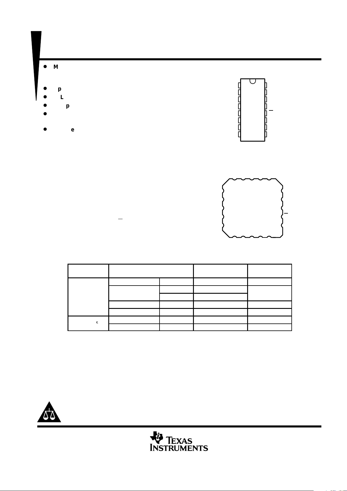
ORDERING INFORMA TION
T
A
PACKAGE
†
ORDERABLE
PART NUMBER
TOP-SIDE
MARKING
PDIP – N Tube AM26LS31CN AM26LS31CN
Tube AM26LS31CD
0°C to 70°C
SOIC
–
D
Tape and reel AM26LS31CDR
AM26LS31C
SOP – NS Tape and reel AM26LS31CNSR 26LS31
SSOP – DB Tape and reel AM26LS31CDBR SA31C
CDIP – J Tube AM26LS31MJ AM26LS31MJB
–
55°C to 125°C
LCCC – FK Tube AM26LS31MFK AM26LS31MFKB
†
Package drawings, standard packing quantities, thermal data, symbolization, and PCB design guidelines are
available at www.ti.com/sc/package.
Copyright 2002, Texas Instruments Incorporated
PRODUCTION DATA information is current as of publication date.
Products conform to specifications per the terms of Texas Instruments
standard warranty. Production processing does not necessarily include
testing of all parameters.
Please be aware that an important notice concerning availability, standard warranty, and use in critical applications of
Texas Instruments semiconductor products and disclaimers thereto appears at the end of this data sheet.
1
2
3
4
5
6
7
8
16
15
14
13
12
11
10
9
1A
1Y
1Z
G
2Z
2Y
2A
GND
V
CC
4A
4Y
4Z
G
3Z
3Y
3A
D, DB, N, NS, OR J PACKAGE
(TOP VIEW)
1920132
17
18
16
15
14
1312119 10
5
4
6
7
8
4Y
4Z
NC
G
3Z
1Z
G
NC
2Z
2Y
1Y1ANCV4A
GND
NC
3A
3Y
2A
FK PACKAGE
(TOP VIEW)
CC
On products compliant to MIL-PRF-38535, all parameters are tested
unless otherwise noted. On all other products, production
processing does not necessarily include testing of all parameters.
AM26LS31C, AM26LS31M
QUADRUPLE DIFFERENTIAL LINE DRIVER
SLLS114H – JANUARY 1979 – REVISED JULY 2002
2
POST OFFICE BOX 655303 • DALLAS, TEXAS 75265
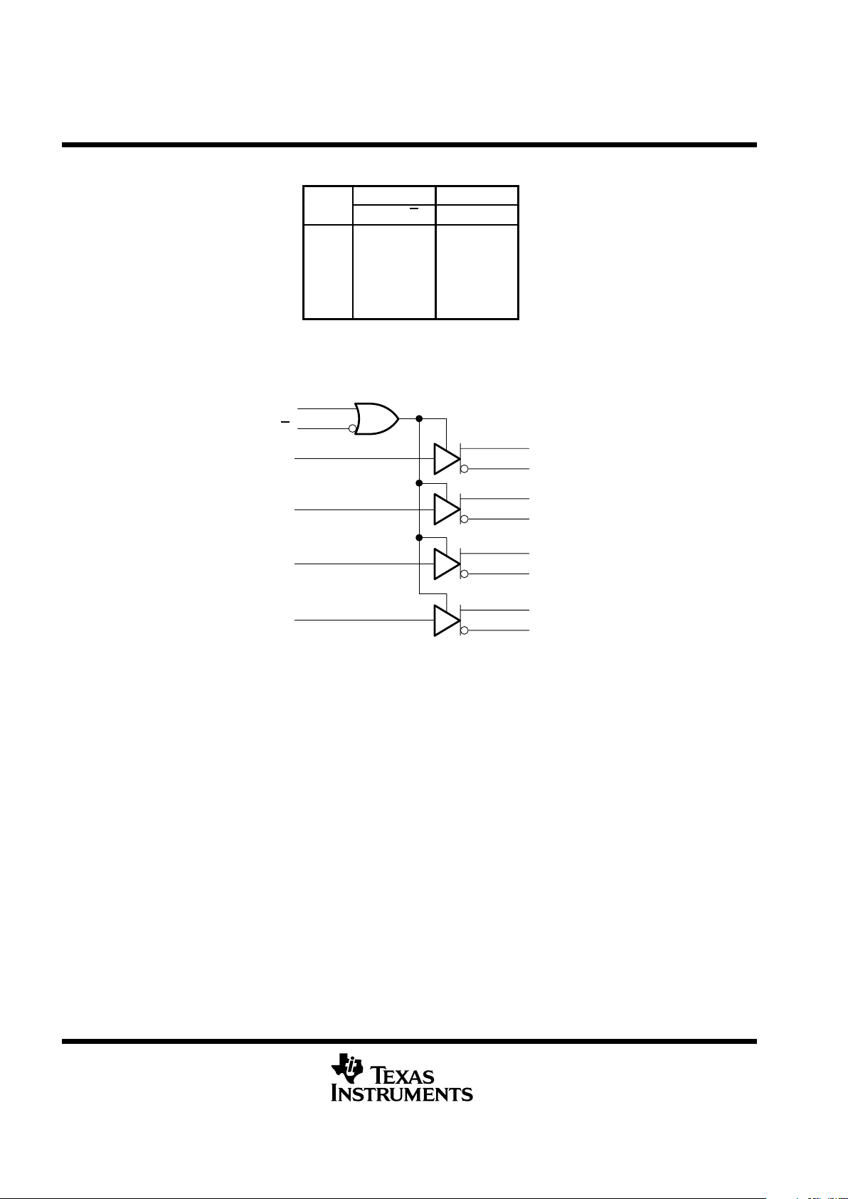
FUNCTION TABLE
(each driver)
INPUT
ENABLES OUTPUTS
A
G G Y Z
H H X H L
L H XLH
H X LHL
L X LLH
X L H Z Z
H = high level, L = low level, X = irrelevant,
Z = high impedance (off)
logic diagram (positive logic)
1Z
1Y
G
G
1A
4
12
1
2
3
2Z
2Y
2A
7
6
5
3Z
3Y
3A
9
10
11
4Z
4Y
4A
15
14
13
AM26LS31C, AM26LS31M
QUADRUPLE DIFFERENTIAL LINE DRIVER
SLLS114H – JANUARY 1979 – REVISED JULY 2002
3
POST OFFICE BOX 655303 • DALLAS, TEXAS 75265
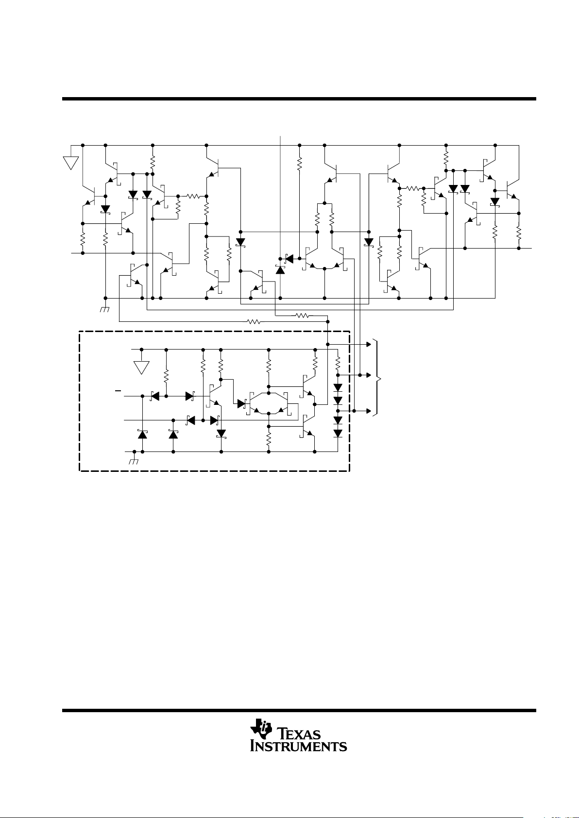
schematic (each driver)
22 kΩ
To Three Other Drivers
Common to All Four Drivers
GND
Enable G
Enable G
V
CC
V
V
Output Y
9 Ω
Input A
22 kΩ
22 kΩ
All resistor values are nominal.
Output Z
9 Ω

AM26LS31C, AM26LS31M
QUADRUPLE DIFFERENTIAL LINE DRIVER
SLLS114H – JANUARY 1979 – REVISED JULY 2002
4
POST OFFICE BOX 655303 • DALLAS, TEXAS 75265
absolute maximum ratings over operating free-air temperature range (unless otherwise noted)
†
Supply voltage, V
CC
(see Note 1) 7 V. . . . . . . . . . . . . . . . . . . . . . . . . . . . . . . . . . . . . . . . . . . . . . . . . . . . . . . . . . . . .
Input voltage, V
I
7 V. . . . . . . . . . . . . . . . . . . . . . . . . . . . . . . . . . . . . . . . . . . . . . . . . . . . . . . . . . . . . . . . . . . . . . . . . . . .
Output off-state voltage 5.5 V. . . . . . . . . . . . . . . . . . . . . . . . . . . . . . . . . . . . . . . . . . . . . . . . . . . . . . . . . . . . . . . . . . . .
Package thermal impedance, θ
JA
(see Note 2): D package 73°C/W. . . . . . . . . . . . . . . . . . . . . . . . . . . . . . . . . . .
DB package 82°C/W. . . . . . . . . . . . . . . . . . . . . . . . . . . . . . . . .
N package 67°C/W. . . . . . . . . . . . . . . . . . . . . . . . . . . . . . . . . . .
NS package 64°C/W. . . . . . . . . . . . . . . . . . . . . . . . . . . . . . . . .
Lead temperature 1,6 mm (1/16 inch) from case for 10 seconds 260°C. . . . . . . . . . . . . . . . . . . . . . . . . . . . . . .
Lead temperature 1,6 mm (1/16 inch) from case for 60 seconds: J package 300°C. . . . . . . . . . . . . . . . . . . . .
Storage temperature range, T
stg
–65°C to 150°C. . . . . . . . . . . . . . . . . . . . . . . . . . . . . . . . . . . . . . . . . . . . . . . . . . .
†
Stresses beyond those listed under “absolute maximum ratings” may cause permanent damage to the device. These are stress ratings only, and
functional operation of the device at these or any other conditions beyond those indicated under “recommended operating conditions” is not
implied. Exposure to absolute-maximum-rated conditions for extended periods may affect device reliability.
NOTES: 1. All voltage values, except differential output voltage VOD, are with respect to network GND.
2. The package thermal impedance is calculated in accordance with JESD 51-7.
DISSIPATION RATING TABLE
T
≤ 25°C DERATING FACTOR T
= 70°C T
= 125°C
PACKAGE
A
POWER RATING ABOVE TA = 25°C
‡
A
POWER RATING
A
POWER RATING
FK 1375 mW 11.0 mW/°C 880 mW 275 mW
J 1375 mW 11.0 mW/°C 880 mW 275 mW
‡
This is the inverse of the traditional junction-to-ambient thermal resistance (RθJA). Thermal resistances are not
production tested and the values given are for informational purposes only .
recommended operating conditions
MIN NOM MAX UNIT
pp
AM26LS31C 4.75 5 5.25
VCCSupply voltage
AM26LS31M 4.5 5 5.5
V
V
IH
High-level input voltage 2 V
V
IL
Low-level input voltage 0.8 V
I
OH
High-level output current –20 mA
I
OL
Low-level output current 20 mA
p
p
AM26LS31C 0 70
TAOperating free-air temperature
AM26LS31M –55 125
°C

AM26LS31C, AM26LS31M
QUADRUPLE DIFFERENTIAL LINE DRIVER
SLLS114H – JANUARY 1979 – REVISED JULY 2002
5
POST OFFICE BOX 655303 • DALLAS, TEXAS 75265
electrical characteristics over operating free-air temperature range (unless otherwise noted)
†
PARAMETER TEST CONDITIONS MIN TYP‡MAX UNIT
V
IK
Input clamp voltage VCC = MIN, II = –18 mA –1.5 V
p
V
= MIN,
TA = –55°C 2.4
VOHHigh-level output voltage
CC
,
IOH = –20 mA
All other temperatures 2.5
V
V
OL
Low-level output voltage VCC = MIN, IOL = 20 mA 0.5 V
p
p
VO = 0.5 V –20
IOZOff-state (high-impedance-state) output current
V
CC
=
MIN
VO = 2.5 V 20
µ
A
I
I
Input current at maximum input voltage VCC = MAX, VI = 7 V 0.1 mA
I
IH
High-level input current VCC = MAX, VI = 2.7 V 20 µA
I
IL
Low-level input current VCC = MAX, VI = 0.4 V –0.36 mA
I
OS
Short-circuit output current
§
VCC = MAX –30 –150 mA
I
CC
Supply current VCC = MAX, All outputs disabled 32 80 mA
†
For C suffix devices, VCC MIN = 4.75 V and VCC MAX = 5.25 V. For M suffix devices, VCC MIN = 4.5 V and VCC MAX = 5.5 V.
‡
All typical values are at VCC = 5 V and TA = 25°C.
§
Not more than one output should be shorted at a time, and duration of the short circuit should not exceed one second.
switching characteristics, VCC = 5 V, TA = 25°C (see Figure 1)
PARAMETER TEST CONDITIONS MIN TYP MAX UNIT
t
PLH
Propagation delay time, low-to-high-level output
p
p
14 20
t
PHL
Propagation delay time, high-to-low-level output
C
L
=
30 pF
,
S1 and S2 open
14 20
ns
t
PZH
Output enable time to high level
p
RL = 75 Ω 25 40
t
PZL
Output enable time to low level
C
L
=
30 pF
RL = 180 Ω 37 45
ns
t
PHZ
Output disable time from high level
p
21 30
t
PLZ
Output disable time from low level
C
L
=
10 pF
,
S1 and S2 closed
23 35
ns
Output-to-output skew CL = 30 pF, S1 and S2 open 1 6 ns

AM26LS31C, AM26LS31M
QUADRUPLE DIFFERENTIAL LINE DRIVER
SLLS114H – JANUARY 1979 – REVISED JULY 2002
6
POST OFFICE BOX 655303 • DALLAS, TEXAS 75265
PARAMETER MEASUREMENT INFORMATION
Waveform 1
(see Note E)
Output Z
Output Y
Input A
(see Notes B
and C)
V
OL
V
OH
V
OL
V
OH
3 V
t
PHL
Skew Skew
t
PLH
t
PLH
t
PHL
0 V
PROPAGATION DELAY TIMES AND SKEW TEST CIRCUIT
V
CC
Test Point
S1
S2
75 Ω
180 Ω
C
L
(see Note A)
From Output
Under Test
V
OH
V
OL
≈1.5 V
0 V
3 V
Enable G
Enable G
(see Note D)
S1 Open
S2 Closed
S1 Closed
S2 Open
t
PZH
t
PZL
t
PHZ
t
PLZ
S1 Closed
S2 Closed
0.5 V
≈0 V
≈4.5 V
S1 Closed
S2 Closed
≈1.5 V
ENABLE AND DISABLE TIME WAVEFORMS
See Note D
NOTES: A. CL includes probe and jig capacitance.
B. All input pulses are supplied by generators having the following characteristics: PRR ≤ 1 MHz, ZO ≈ 50 Ω, tr ≤ 15 ns, tf ≤ 6 ns.
C. When measuring propagation delay times and skew, switches S1 and S2 are open.
D. Each enable is tested separately.
E. Waveform 1 is for an output with internal conditions such that the output is low except when disabled by the output control.
Waveform 2 is for an output with internal conditions such that the output is high except when disabled by the output control.
1.3 V 1.3 V
1.5 V
1.5 V
1.5 V 1.5 V
Waveform 2
(see Note E)
0.5 V
1.5 V
1.5 V
Figure 1. Test Circuit and Voltage Waveforms

AM26LS31C, AM26LS31M
QUADRUPLE DIFFERENTIAL LINE DRIVER
SLLS114H – JANUARY 1979 – REVISED JULY 2002
7
POST OFFICE BOX 655303 • DALLAS, TEXAS 75265
TYPICAL CHARACTERISTICS
Figure 2
VI – Enable G Input Voltage – V
OUTPUT VOLTAGE
vs
ENABLE G INPUT VOLTAGE
VCC = 5.25 V
VCC = 5 V
VCC = 4.75 V
Load = 470 Ω to GND
TA = 25°C
See Note A
– Y Output Voltage – V
V
O
4
3
2
1
0
0123
Figure 3
VI – Enable G Input Voltage – V
OUTPUT VOLTAGE
vs
ENABLE G INPUT VOLTAGE
VCC = 5 V
Load = 470 Ω to GND
See Note A
TA = 70°C
TA = 0°C
TA = 25°C
– Y Output Voltage – VV
O
4
3
2
1
0
0123
Figure 4
VI – Enable G Input Voltage – V
– Output Voltage – V
OUTPUT VOLTAGE
vs
ENABLE G INPUT VOLTAGE
V
O
VCC = 5.25 V
VCC = 5 V
VCC = 4.75 V
4
3
2
1
0
0123
5
6
Load = 470 Ω to V
CC
TA = 25°C
See Note B
Figure 5
VI – Enable G Input Voltage – V
OUTPUT VOLTAGE
vs
ENABLE G INPUT VOLTAGE
TA = 25°C
TA = 0°C
TA = 70°C
– Output Voltage – VV
O
4
3
2
1
0
0123
5
6
VCC = 5 V
Load = 470 Ω to V
CC
See Note B
NOTES: A. The A input is connected to VCC during testing of the Y outputs and to ground during testing of the Z outputs.
B. The A input is connected to ground during testing of the Y outputs and to VCC during testing of the Z outputs.

AM26LS31C, AM26LS31M
QUADRUPLE DIFFERENTIAL LINE DRIVER
SLLS114H – JANUARY 1979 – REVISED JULY 2002
8
POST OFFICE BOX 655303 • DALLAS, TEXAS 75265
TYPICAL CHARACTERISTICS
Figure 6
– High-Level Output Voltage – V
TA – Free-Air Temperature – °C
IOH = –20 mA
IOH = –40 mA
HIGH-LEVEL OUTPUT VOLTAGE
vs
FREE-AIR TEMPERATURE
V
OH
VCC = 5 V
See Note A
4
3
2
1
0
0255075
5
Figure 7
IOH – High-Level Output Current – mA
HIGH-LEVEL OUTPUT VOLTAGE
vs
HIGH-LEVEL OUTPUT CURRENT
VCC = 5.25 V
VCC = 4.75 V
VCC = 5 V
TA = 25°C
See Note A
– High-Level Output Voltage – V
V
OH
4
3
2
1
0
0 –20
–40 –60 –80 –100
Figure 8
– Low-Level Output Voltage – V
TA – Free-Air Temperature – °C
VCC = 5 V
IOL = 40 mA
See Note B
LOW-LEVEL OUTPUT VOLTAGE
vs
FREE-AIR TEMPERATURE
V
OL
0.4
0.3
0.2
0.1
0
25 50 75
0.5
0
Figure 9
IOL – Low-Level Output Current – mA
LOW-LEVEL OUTPUT VOLTAGE
vs
LOW-LEVEL OUTPUT CURRENT
VCC = 5.25 V
ÎÎÎÎ
VCC = 4.75 V
TA = 25°C
See Note B
– Low-Level Output Voltage – VV
OL
0.4
0.3
0.2
0.1
0
40 80 120
0.5
0 1006020
0.6
0.7
0.8
0.9
1
NOTES: A. The A input is connected to VCC during testing of the Y outputs and to ground during testing of the Z outputs.
B. The A input is connected to ground during testing of the Y outputs and to VCC during testing of the Z inputs.

AM26LS31C, AM26LS31M
QUADRUPLE DIFFERENTIAL LINE DRIVER
SLLS114H – JANUARY 1979 – REVISED JULY 2002
9
POST OFFICE BOX 655303 • DALLAS, TEXAS 75265
TYPICAL CHARACTERISTICS
VCC = 5 V
Figure 10
VI – Data Input Voltage – V
Y OUTPUT VOLTAGE
vs
DATA INPUT VOLTAGE
VCC = 4.75 V
No Load
TA = 25°C
VCC = 5.25 V
– Y Output Voltage – V
V
O
4
3
2
1
0
0123
5
Figure 11
Y OUTPUT VOLTAGE
vs
DATA INPUT VOLTAGE
TA = 25°C
No Load
TA = 0°C
TA = 70°C
VI – Data Input Voltage – V
– Y Output Voltage – VV
O
4
3
2
1
0
0123
5

IMPORTANT NOTICE
Texas Instruments Incorporated and its subsidiaries (TI) reserve the right to make corrections, modifications,
enhancements, improvements, and other changes to its products and services at any time and to discontinue
any product or service without notice. Customers should obtain the latest relevant information before placing
orders and should verify that such information is current and complete. All products are sold subject to TI’s terms
and conditions of sale supplied at the time of order acknowledgment.
TI warrants performance of its hardware products to the specifications applicable at the time of sale in
accordance with TI’s standard warranty . Testing and other quality control techniques are used to the extent TI
deems necessary to support this warranty. Except where mandated by government requirements, testing of all
parameters of each product is not necessarily performed.
TI assumes no liability for applications assistance or customer product design. Customers are responsible for
their products and applications using TI components. T o minimize the risks associated with customer products
and applications, customers should provide adequate design and operating safeguards.
TI does not warrant or represent that any license, either express or implied, is granted under any TI patent right,
copyright, mask work right, or other TI intellectual property right relating to any combination, machine, or process
in which TI products or services are used. Information published by TI regarding third–party products or services
does not constitute a license from TI to use such products or services or a warranty or endorsement thereof.
Use of such information may require a license from a third party under the patents or other intellectual property
of the third party, or a license from TI under the patents or other intellectual property of TI.
Reproduction of information in TI data books or data sheets is permissible only if reproduction is without
alteration and is accompanied by all associated warranties, conditions, limitations, and notices. Reproduction
of this information with alteration is an unfair and deceptive business practice. TI is not responsible or liable for
such altered documentation.
Resale of TI products or services with statements different from or beyond the parameters stated by TI for that
product or service voids all express and any implied warranties for the associated TI product or service and
is an unfair and deceptive business practice. TI is not responsible or liable for any such statements.
Mailing Address:
Texas Instruments
Post Office Box 655303
Dallas, Texas 75265
Copyright 2002, Texas Instruments Incorporated
 Loading...