

AM26C32C, AM26C32I, AM26C32M
QUADRUPLE DIFFERENTIAL LINE RECEIVERS
SLLS104F – DECEMBER 1990 – REVISED APRIL 1998
D
Meet or Exceed the Requirements of ANSI
EIA/TIA-422-B, EIA/TIA-423-B, and ITU
Recommendation V.10 and V.11
D
Low Power, ICC = 10 mA Typ
D
±7-V Common-Mode Range With ±200-mV
Sensitivity
D
Input Hysteresis...60 mV Typ
D
tpd = 17 ns Typ
D
Operate From a Single 5-V Supply
D
3-State Outputs
D
Input Fail-Safe Circuitry
D
Improved Replacements for AM26LS32
description
The AM26C32C, AM26C32I, and AM26C32M are
quadruple differential line receivers for balanced
or unbalanced digital data transmission. The
enable function is common to all four receivers
and offers a choice of active-high or active-low
input. The 3-state outputs permit connection
directly to a bus-organized system. Fail-safe
design specifies that if the inputs are open, the
outputs are always high.
The AM26C32 is manufactured using a BiCMOS
process, which is a combination of bipolar and
CMOS transistors. This process provides the high
voltage and current of bipolar with the low power
of CMOS to reduce the power consumption to
about one-fifth that of the standard AM26LS32
while maintaining ac and dc performance.
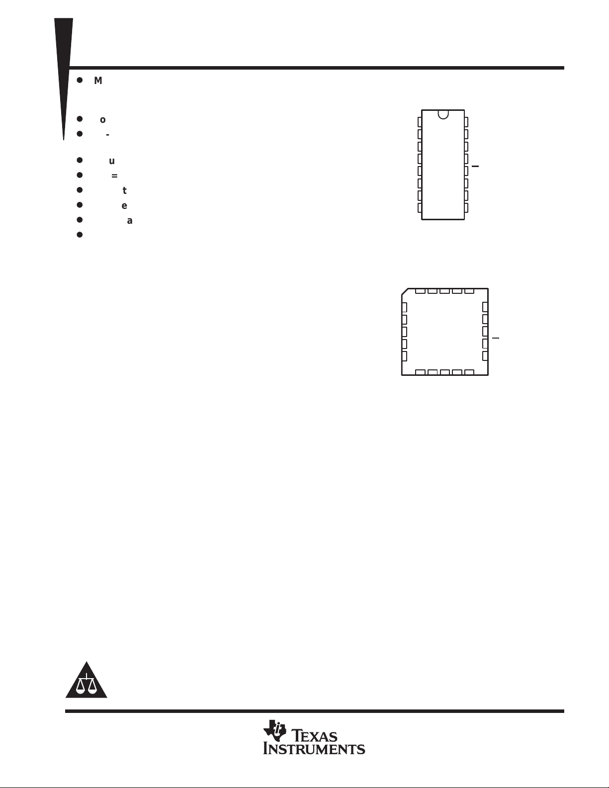
AM26C32C, AM26C32I ... D OR N PACKAGE
AM26C32M ...J OR W PACKAGE
1Y
G
NC
2Y
2A
NC – No internal connection
(TOP VIEW)
1
1B
2
1A
3
1Y
4
G
5
2Y
6
2A
7
2B
GND
8
FK PACKAGE
(TOP VIEW)
1A1BNC
3212019
4
5
6
7
8
910111213
2B
GND
16
15
14
13
12
11
10
NC
9
CC
V
3B
V
4B
4A
4Y
G
3Y
3A
3B
4B
18
17
16
15
14
3A
CC
4A
4Y
NC
G
3Y
The AM26C32C is characterized for operation from 0°C to 70°C. The AM26C32I is characterized for operation
from –40°C to 85°C. The AM26C32M is characterized for operation from –55°C to 125°C.
Please be aware that an important notice concerning availability, standard warranty, and use in critical applications of
Texas Instruments semiconductor products and disclaimers thereto appears at the end of this data sheet.
PRODUCTION DATA information is current as of publication date.
Products conform to specifications per the terms of Texas Instruments
standard warranty. Production processing does not necessarily include
testing of all parameters.
POST OFFICE BOX 655303 • DALLAS, TEXAS 75265
Copyright 1998, Texas Instruments Incorporated
1
AM26C32C, AM26C32I, AM26C32M
OUTPUT
V
V
V
V
V
V
V
QUADRUPLE DIFFERENTIAL LINE RECEIVERS
SLLS104F – DECEMBER 1990 – REVISED APRIL 1998
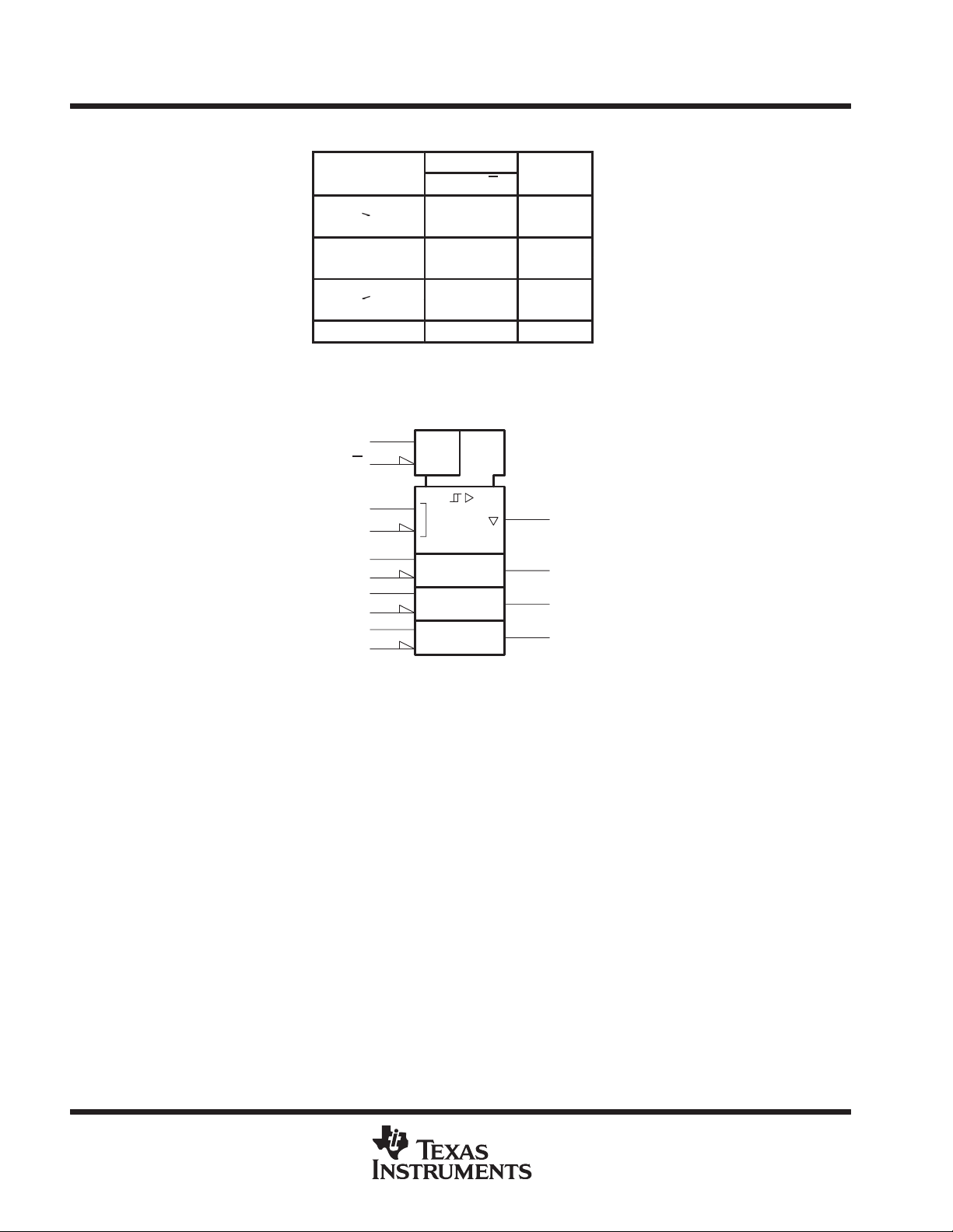
FUNCTION TABLE
(each receiver)
DIFFERENTIAL
INPUT
≥
ID
IT+
<
IT–
H = high level, L = low level, X = irrelevant
Z = high impedance (off), ? = indeterminate
<
ID
≤
ID
IT–
X LHZ
ENABLES
G G
H X H
X LH
HX?
IT+
X L?
HXL
X LL
logic symbol
†
This symbol is in accordance with ANSI/IEEE Std 91-1984 and IEC Publication 617-12.
Pin numbers shown are for the D, J, N, and W packages.
†
1A
1B
2A
2B
3A
3B
4A
4B
4
G
12
G
2
1
6
7
10
9
14
15
≥ 1
EN
11
13
3
1Y
5
2Y
3Y
4Y
2
POST OFFICE BOX 655303 • DALLAS, TEXAS 75265
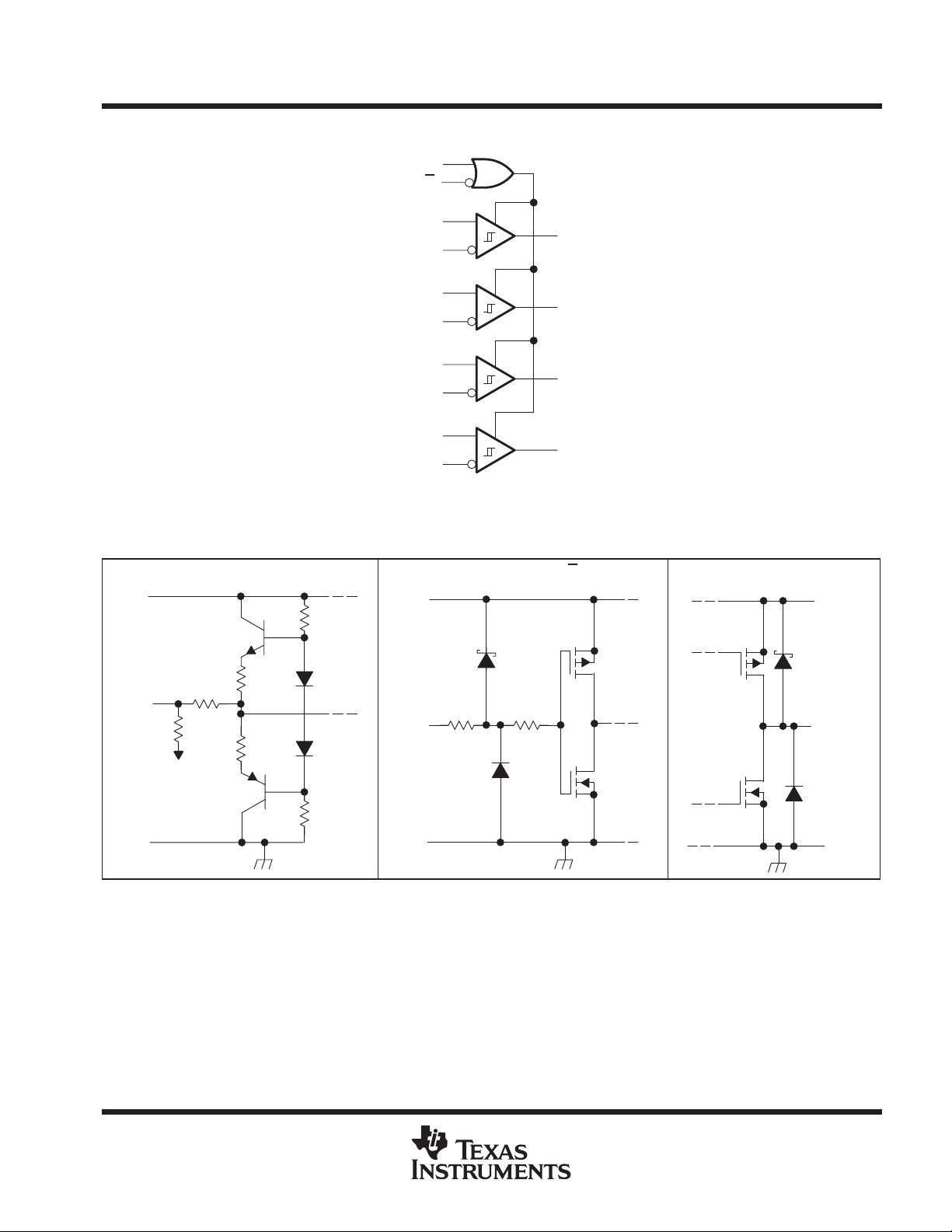
logic diagram (positive logic)
1A
1B
2A
2B
3A
3B
4A
4B
AM26C32C, AM26C32I, AM26C32M
QUADRUPLE DIFFERENTIAL LINE RECEIVERS
SLLS104F – DECEMBER 1990 – REVISED APRIL 1998
4
G
12
G
2
1
6
7
10
9
14
15
11
13
3
1Y
5
2Y
3Y
4Y
Pin numbers shown are for the D, J, N, and W packages.
schematics
EQUIVALENT OF A OR B INPUT
V
CC
Input
288 kΩ
GND
NOM
V
CC(A)
or
GND(B)
17 kΩ
NOM
1.7 kΩ
NOM
1.7 kΩ
NOM
V
Input
GND
EQUIVALENT OF G OR G
CC
INPUT
TYPICAL OF ALL OUTPUTS
V
CC
Output
GND
POST OFFICE BOX 655303 • DALLAS, TEXAS 75265
3

AM26C32C, AM26C32I, AM26C32M
QUADRUPLE DIFFERENTIAL LINE RECEIVERS
SLLS104F – DECEMBER 1990 – REVISED APRIL 1998
absolute maximum ratings over operating free-air temperature range (unless otherwise noted)
Supply voltage, V
Input voltage range, V
Differential input voltage range, V
Output voltage range, V
Output current, I
(see Note 1) 7 V. . . . . . . . . . . . . . . . . . . . . . . . . . . . . . . . . . . . . . . . . . . . . . . . . . . . . . . . . . . . .
CC
: A or B inputs –1 1 V to 14 V. . . . . . . . . . . . . . . . . . . . . . . . . . . . . . . . . . . . . . . . . . . . . . . . .
I
G or G
O
±25 mA. . . . . . . . . . . . . . . . . . . . . . . . . . . . . . . . . . . . . . . . . . . . . . . . . . . . . . . . . . . . . . . . . . . . . . .
O
inputs –0.5 V to VCC + 0.5 V. . . . . . . . . . . . . . . . . . . . . . . . . . . . . . . . . . . . . . . .
–14 V to 14 V. . . . . . . . . . . . . . . . . . . . . . . . . . . . . . . . . . . . . . . . . . . . . . . . . .
ID
–0.5 V to VCC + 0.5 V. . . . . . . . . . . . . . . . . . . . . . . . . . . . . . . . . . . . . . . . . . . . . . . . . . .
†
Continuous total power dissipation See Dissipation Rating Table. . . . . . . . . . . . . . . . . . . . . . . . . . . . . . . . . . . . .
Storage temperature range, T
–65°C to 150°C. . . . . . . . . . . . . . . . . . . . . . . . . . . . . . . . . . . . . . . . . . . . . . . . . . .
stg
Lead temperature 1,6 mm (1/16 inch) from case for 10 seconds 260°C. . . . . . . . . . . . . . . . . . . . . . . . . . . . . . .
†
Stresses beyond those listed under “absolute maximum ratings” may cause permanent damage to the device. These are stress ratings only, and
functional operation of the device at these or any other conditions beyond those indicated under “recommended operating conditions” is not
implied. Exposure to absolute-maximum-rated conditions for extended periods may affect device reliability.
NOTE 1: All voltage values, except differential output voltage, VOD, are with respect to network GND. Currents into the device are positive and
currents out of the device are negative.
DISSIPATION RATING TABLE
PACKAGE
D 950 mW 7.6 mW/°C 608 mW 494 mW —
N 1150 mW 9.2 mW/°C 736 mW 598 mW —
J 1375 mW 11 mW/°C — — 275 mW
W 1000 mW 8.0 mW/°C — — 200 mW
TA ≤ 25°C
POWER RATING
DERATING FACTOR
ABOVE TA = 25°C
TA = 70°C
POWER RATING
TA = 85°C
POWER RATING
POWER RATING
TA = 125°C
recommended operating conditions
Supply voltage, V
High-level input voltage, V
Low-level input voltage, V
Common-mode input voltage, V
High-level output current, I
Low-level output current, I
Operating free-air temperature, T
CC
IH
IL
IC
OH
OL
A
MIN NOM MAX UNIT
4.5 5 5.5 V
2 V
0.8 V
±7 V
–6 mA
AM26C32C 0 70
AM26C32I –40 85
AM26C32M –55 125
6 mA
°C
4
POST OFFICE BOX 655303 • DALLAS, TEXAS 75265

V
Differential input high-threshold voltage
OOH
,
V
V
Differential input low-threshold voltage
O
,
V
IILine input current
mA
CONDITIONS
See Figure 1
See Figure 1
See Figure 2
See Figure 2
AM26C32C, AM26C32I, AM26C32M
QUADRUPLE DIFFERENTIAL LINE RECEIVERS
SLLS104F – DECEMBER 1990 – REVISED APRIL 1998
electrical characteristics over recommended ranges of VCC, VIC, and operating free-air
temperature (unless otherwise noted)
PARAMETER TEST CONDITIONS MIN TYP†MAX UNIT
V
IT+
IT–
V
V
V
V
I
I
I
r
I
†
All typical values are at VCC = 5 V, VIC = 0, and TA = 25°C.
‡
The algebraic convention, in which the less positive (more negative) limit is designated minimum, is used in this data sheet for common-mode
input voltage.
Hysteresis voltage (V
hys
Enable input clamp voltage VCC = 4.5 V, II = –18 mA –1.5 V
IK
High-level output voltage VID = 200 mV, IOH = –6 mA 3.8 V
OH
Low-level output voltage VID = –200 mV, IOL = 6 mA 0.2 0.3 V
OL
Off-state (high-impedance-state) output current VO = VCC or GND ±0.5 ±5 µA
OZ
High-level enable current VI = 2.7 V 20 µA
IH
Low-level enable current VI = 0.4 V –100 µA
IL
Input resistance One input to ground 12 17 kΩ
i
Supply current VCC = 5.5 V 10 15 mA
CC
p
p
– V
IT+
p
) 60 mV
IT–
= V
IOH = –440 µA
V
= 0.45 V,
IOL = 8 mA
VI = 10 V, Other input at 0 V 1.5
VI = –10 V, Other input at 0 V –2.5
VIC = full range 0.2
min,
VIC = 0 to 5.5 V 0.1
VIC = full range –0.2
VIC = 0 to 5.5 V –0.1
‡
‡
switching characteristics over recommended ranges of operation conditions, CL = 50 pF (unless
otherwise noted)
PARAMETER
t
Propagation delay time, low- to high-level output
PLH
t
Propagation delay time, high- to low-level output
PHL
t
Output transition time, low- to high-level output
TLH
t
Output transition time, high- to low-level output
THL
t
Output enable time to high level
PZH
t
Output enable time to low level
PZL
t
Output disable time from high level
PHZ
t
Output disable time from low level
PLZ
§
All typical values are at VCC = 5 V, TA = 25°C.
TEST
AM26C32C
AM26C32I
MIN TYP§MAX MIN TYP§MAX
9 17 27 9 17 27 ns
9 17 27 9 17 27 ns
4 9 4 10 ns
4 9 4 9 ns
13 22 13 22 ns
13 22 13 22 ns
13 22 13 26 ns
13 22 13 25 ns
AM26C32M
UNIT
POST OFFICE BOX 655303 • DALLAS, TEXAS 75265
5

AM26C32C, AM26C32I, AM26C32M
QUADRUPLE DIFFERENTIAL LINE RECEIVERS
SLLS104F – DECEMBER 1990 – REVISED APRIL 1998
PARAMETER MEASUREMENT INFORMATION
V
CC
A
Device
Under
B
Input
NOTE A: CL includes probe and jig capacitance.
Test
TEST CIRCUIT
CL = 50 pF
(see Note A)
Figure 1. Switching Test Circuit and Voltage Waveforms
G Input
Input
G
VID = ±2.5 V
A Input
B Input
V
CC
Device
Under
Test
Output
Input
S1
RL = 1 kΩ
CL = 50 pF
(see Note A)
t
t
PZL
t
PZH
PLH
t
TLH
10%
VOLTAGE WAVEFORMS
, t
Measurement: S1 to V
PLZ
, t
Measurement: S1 to GND
PHZ
t
THL
V
90%90%
10%
t
PHL
CC
OH
50%
V
OL
2.5 V
0 V
± 2.5 V
Output
Output
G
t
PZH
50%
t
PZL
50%
(see Note B)
(with VID = 2.5 V)
(with VID = –2.5 V)
NOTES: A. CL includes probe and jig capacitance.
B. The input pulse is supplied by a generator having the following characteristics: PRR = 1 MHz, duty cycle ≤ 50%, tr = tf = 6 ns.
Figure 2. Enable/Disable Time Test Circuit and Output V oltage Waveforms
TEST CIRCUIT
1.3 VG
t
PHZ
VOH –0.5 V
t
PLZ
VOL + 0.5 V
VOLTAGE WAVEFORMS
t
PZH
t
PZL
1.3 V
t
PHZ
VOH –0.5 V
t
PLZ
VOL + 0.5 V
3 V
0 V
3 V
0 V
V
V
V
V
OH
OL
OH
OL
6
POST OFFICE BOX 655303 • DALLAS, TEXAS 75265

IMPORTANT NOTICE
T exas Instruments and its subsidiaries (TI) reserve the right to make changes to their products or to discontinue
any product or service without notice, and advise customers to obtain the latest version of relevant information
to verify, before placing orders, that information being relied on is current and complete. All products are sold
subject to the terms and conditions of sale supplied at the time of order acknowledgement, including those
pertaining to warranty, patent infringement, and limitation of liability.
TI warrants performance of its semiconductor products to the specifications applicable at the time of sale in
accordance with TI’s standard warranty. Testing and other quality control techniques are utilized to the extent
TI deems necessary to support this warranty . Specific testing of all parameters of each device is not necessarily
performed, except those mandated by government requirements.
CERT AIN APPLICATIONS USING SEMICONDUCTOR PRODUCTS MAY INVOLVE POTENTIAL RISKS OF
DEATH, PERSONAL INJURY, OR SEVERE PROPERTY OR ENVIRONMENTAL DAMAGE (“CRITICAL
APPLICATIONS”). TI SEMICONDUCTOR PRODUCTS ARE NOT DESIGNED, AUTHORIZED, OR
WARRANTED TO BE SUITABLE FOR USE IN LIFE-SUPPORT DEVICES OR SYSTEMS OR OTHER
CRITICAL APPLICA TIONS. INCLUSION OF TI PRODUCTS IN SUCH APPLICATIONS IS UNDERST OOD TO
BE FULLY AT THE CUSTOMER’S RISK.
In order to minimize risks associated with the customer’s applications, adequate design and operating
safeguards must be provided by the customer to minimize inherent or procedural hazards.
TI assumes no liability for applications assistance or customer product design. TI does not warrant or represent
that any license, either express or implied, is granted under any patent right, copyright, mask work right, or other
intellectual property right of TI covering or relating to any combination, machine, or process in which such
semiconductor products or services might be or are used. TI’s publication of information regarding any third
party’s products or services does not constitute TI’s approval, warranty or endorsement thereof.
Copyright 1998, Texas Instruments Incorporated
 Loading...