

AM26C31C, AM26C31I, AM26C31M
QUADRUPLE DIFFERENTIAL LINE DRIVERS
SLLS103G – DECEMBER 1990 – REVISED SEPTEMBER 1998
D
Meet or Exceed the Requirements of
TIA/EIA-422-B and ITU Recommendation
V.11
D
Low Power, ICC = 100 µA Typ
D
Operate From a Single 5-V Supply
D
High Speed, t
D
Low Pulse Distortion, t
D
High Output Impedance in Power-Off
PLH
= t
= 7 ns Typ
PHL
sk(p)
= 0.5 ns Typ
Conditions
D
Improved Replacement for AM26LS31
description
The AM26C31C, AM26C31I, and AM26C31M are
four complementary-output line drivers designed
to meet the requirements of TIA/EIA -422-B and
ITU (formerly CCITT). The 3-state outputs have
high-current capability for driving balanced lines,
such as twisted-pair or parallel-wire transmission
lines, and they provide the high-impedance state
in the power-off condition. The enable function is
common to all four drivers and offers the choice of
an active-high or active-low enable input.
BiCMOS circuitry reduces power consumption
without sacrificing speed.
The AM26C31C is characterized for operation
from 0°C to 70°C, the AM26C31I is characterized
for operation from –40°C to 85°C, and the
AM26C31M is characterized for operation from
–55°C to 125°C.
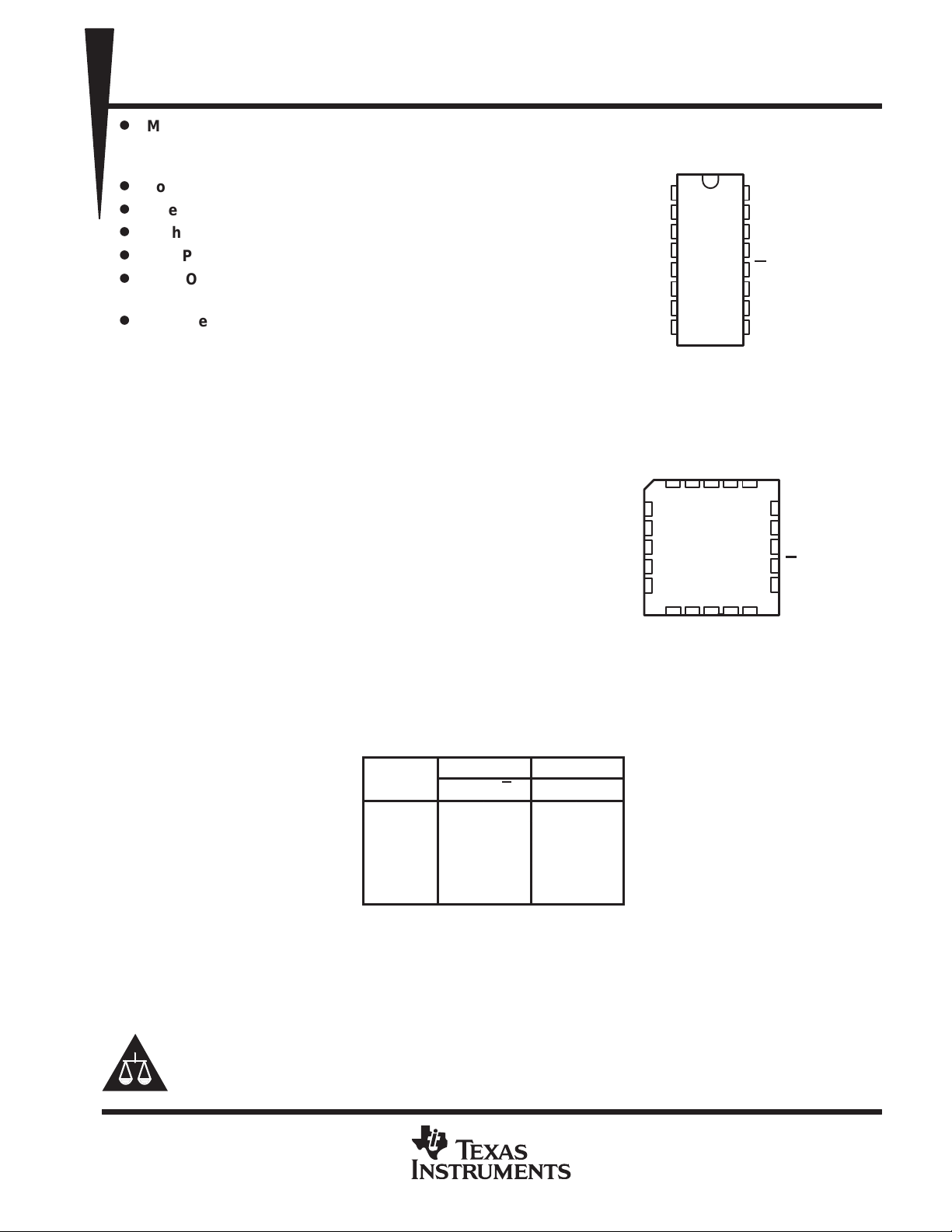
AM26C31C, AM26C31I . . . D, DB†, OR N PACKAGE
†
AM26C31M ...J OR W PACKAGE
The DB package is only available left-ended taped
(order AM26C31IDBLE or AM26C31CDBLE).
AM26C31M . . . FK PACKAGE
1Z
G
NC
2Z
2Y
NC – No internal connection
(TOP VIEW)
1A
1
2
1Y
3
1Z
4
G
5
2Z
6
2Y
7
2A
GND
8
(TOP VIEW)
1Y1ANC
3212019
4
5
6
7
8
910111213
2A
GND
NC
16
15
14
13
12
11
10
9
V
3A
CC
V
4A
4Y
4Z
G
3Z
3Y
3A
4A
18
17
16
15
14
3Y
CC
4Y
4Z
NC
G
3Z
Please be aware that an important notice concerning availability, standard warranty, and use in critical applications of
Texas Instruments semiconductor products and disclaimers thereto appears at the end of this data sheet.
PRODUCTION DATA information is current as of publication date.
Products conform to specifications per the terms of Texas Instruments
standard warranty. Production processing does not necessarily include
testing of all parameters.
FUNCTION TABLE
(each driver)
INPUT
A
H H X H L
L H XLH
H XLHL
L XLLH
X LHZZ
H = high level, L = low level, X = irrelevant,
Z = high impedance (off)
ENABLES OUTPUTS
G G Y Z
Copyright 1998, Texas Instruments Incorporated
POST OFFICE BOX 655303 • DALLAS, TEXAS 75265
1
AM26C31C, AM26C31I, AM26C31M
QUADRUPLE DIFFERENTIAL LINE DRIVERS
SLLS103G – DECEMBER 1990 – REVISED SEPTEMBER 1998
4
12
1
7
9
15
†
≥ 1
EN
2
1Y
3
1Z
6
2Y
5
2Z
10
3Y
11
3Z
14
4Y
13
4Z
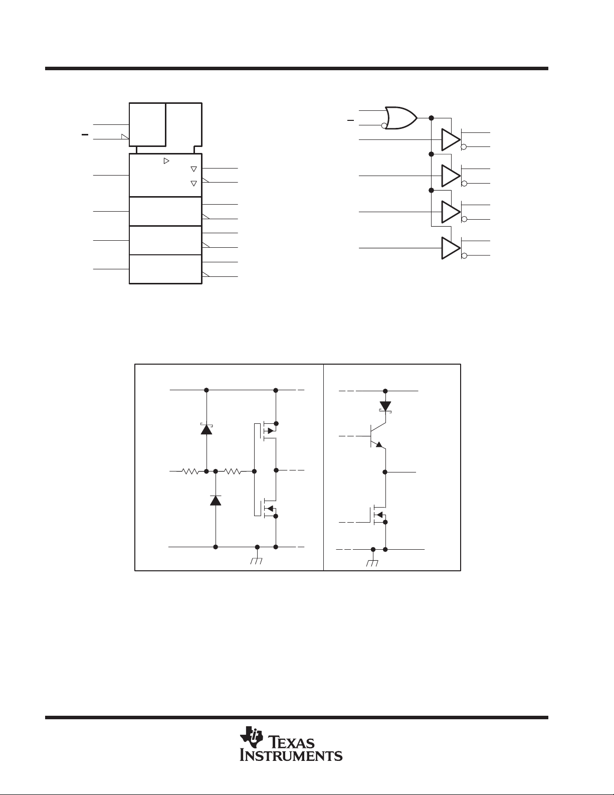
logic symbol
G
G
1A
2A
3A
4A
†
This symbol is in accordance with ANSI/IEEE Std 91-1984
and IEC Publication 617-12.
The terminal numbers shown are for the D, DB, J, N, and W packages.
schematics of inputs and outputs
logic diagram (positive logic)
4
G
12
G
1
1A
7
2A
9
3A
15
4A
10
11
14
13
2
1Y
3
1Z
6
2Y
5
2Z
3Y
3Z
4Y
4Z
EQUIVALENT OF EACH INPUT
V
CC
Input
GND
TYPICAL OF ALL OUTPUTS
V
CC
Output
GND
2
POST OFFICE BOX 655303 • DALLAS, TEXAS 75265
AM26C31C, AM26C31I, AM26C31M
QUADRUPLE DIFFERENTIAL LINE DRIVERS
SLLS103G – DECEMBER 1990 – REVISED SEPTEMBER 1998
absolute maximum ratings over operating free-air temperature range (unless otherwise noted)
Supply voltage range, V
Input voltage range, V
Differential input voltage range, V
Output voltage range, V
Input or output clamp current, I
Output current, I
V
current 200 mA. . . . . . . . . . . . . . . . . . . . . . . . . . . . . . . . . . . . . . . . . . . . . . . . . . . . . . . . . . . . . . . . . . . . . . . . . . . .
CC
±150 mA. . . . . . . . . . . . . . . . . . . . . . . . . . . . . . . . . . . . . . . . . . . . . . . . . . . . . . . . . . . . . . . . . . . . . .
O
GND current –200 mA. . . . . . . . . . . . . . . . . . . . . . . . . . . . . . . . . . . . . . . . . . . . . . . . . . . . . . . . . . . . . . . . . . . . . . . . . .
Continuous total power dissipation See Dissipation Rating Table. . . . . . . . . . . . . . . . . . . . . . . . . . . . . . . . . . . . .
Storage temperature range, T
Lead temperature 1,6 mm (1/16 inch) from case for 10 seconds 260°C. . . . . . . . . . . . . . . . . . . . . . . . . . . . . . .
†
Stresses beyond those listed under “absolute maximum ratings” may cause permanent damage to the device. These are stress ratings only, and
functional operation of the device at these or any other conditions beyond those indicated under “recommended operating conditions” is not
implied. Exposure to absolute-maximum-rated conditions for extended periods may affect device reliability.
NOTE 1: All voltage values, except differential output voltage (VOD), are with respect to the network ground terminal.
PACKAGE
D
DB
N
FK
J
W
TA ≤ 25°C
POWER RATING
1150 mW
1375 mW
1375 mW
1000 mW
(see Note 1) –0.5 V to 7 V. . . . . . . . . . . . . . . . . . . . . . . . . . . . . . . . . . . . . . . . . . . . . .
CC
–0.5 V to VCC + 0.5 V. . . . . . . . . . . . . . . . . . . . . . . . . . . . . . . . . . . . . . . . . . . . . . . . . . . . . . .
I
–0.5 V to 7 V. . . . . . . . . . . . . . . . . . . . . . . . . . . . . . . . . . . . . . . . . . . . . . . . . . . . . . . . . . .
O
950 mW
781 mW
–14 V to 14 V. . . . . . . . . . . . . . . . . . . . . . . . . . . . . . . . . . . . . . . . . . . . . . . . . .
ID
or IOK ±20 mA. . . . . . . . . . . . . . . . . . . . . . . . . . . . . . . . . . . . . . . . . . . . . . . . . . . .
IK
–65°C to 150°C. . . . . . . . . . . . . . . . . . . . . . . . . . . . . . . . . . . . . . . . . . . . . . . . . . .
stg
DISSIPATION RATING TABLE
DERATING FACTOR
ABOVE TA = 25°C
7.6 mW/°C
6.2 mW/°C
9.2 mW/°C
11 mW/°C
11 mW/°C
8.0 mW/°C
TA = 70°C
POWER RATING
608 mW
502 mW
736 mW
—
—
—
TA = 85°C
POWER RATING
494 mW
409 mW
598 mW
—
—
—
TA = 125°C
POWER RATING
—
—
—
275 mW
275 mW
200 mW
†
recommended operating conditions
Supply voltage, V
Differential input voltage, V
High-level input voltage, V
Low-level input voltage, V
High-level output current, I
Low-level output current, I
Operating free-air temperature, T
CC
IL
ID
IH
OH
OL
AM26C31C 0 70
AM26C31I –40 85
A
AM26C31M –55 125
MIN NOM MAX UNIT
4.5 5 5.5 V
±7 V
2 V
0.8 V
–20 mA
20 mA
°C
POST OFFICE BOX 655303 • DALLAS, TEXAS 75265
3

AM26C31C, AM26C31I, AM26C31M
R
100 Ω
See Figure 1
I
Driver output current with power off
A
IOZHigh-impedance off-state output current
O
,
I
,
1.53mA
S1 is closed
See Figure 4
QUADRUPLE DIFFERENTIAL LINE DRIVERS
SLLS103G – DECEMBER 1990 – REVISED SEPTEMBER 1998
electrical characteristics over recommended ranges of supply voltage and operating free-air
temperature (unless otherwise noted)
AM26C31C
PARAMETER TEST CONDITIONS
V
OH
V
OL
|VOD| Differential output voltage magnitude 2 3.1 V
∆|VOD| Change in magnitude of differential output voltage
V
OC
∆|VOC| Change in magnitude of common-mode output voltage
I
I
O(off)
I
OS
I
CC
C
i
†
All typical values are at VCC = 5 V and TA = 25°C.
‡
∆|VOD| and ∆|VOC| are the changes in magnitude of VOD and VOC, respectively, that occur when the input is changed from a high level to a low
level.
NOTE 2: This parameter is measured per input. All other inputs are at 0 or 5 V .
High-level output voltage IO = –20 mA 2.4 3.4 V
Low-level output voltage IO = 20 mA 0.2 0.4 V
‡
Common-mode output voltage
Input current VI = VCC or GND ±1 µA
p
Driver output short-circuit current VO = 0 –30 –150 mA
p
Quiescent supply current
Input capacitance 6 pF
p
p
=
L
‡
VCC = 0, VO = 6 V 100
VCC = 0, VO = –0.25 V –100
VO = 2.5 V 20 µA
VO = 0.5 V –20 µA
IO = 0, VI = 0 V or 5 V 100 µA
= 0, V
I
See Note 2
,
= 2.4 V or 0.5 V,
AM26C31I
MIN TYP†MAX
±0.4 V
±0.4 V
UNIT
3 V
µ
switching characteristics over recommended ranges of supply voltage and operating free-air
temperature (unless otherwise noted)
AM26C31C
PARAMETER TEST CONDITIONS
t
PLH
t
PHL
t
sk(p)
t
, t
r(OD)
f(OD)
t
PZH
t
PZL
t
PHZ
t
PLZ
C
pd
†
All typical values are at VCC = 5 V and TA = 25°C.
NOTE 3: Cpd is used to estimate the switching losses according to PD = Cpd × V
Propagation delay time, low- to high-level output 3 7 12 ns
Propagation delay time, high- to low-level output
Pulse skew time (|t
Differential output rise and fall times S1 is open, See Figure 3 5 10 ns
Output enable time to high level 10 19 ns
Output enable time to low level
Output disable time from high level
Output disable time from low level 7 16 ns
Power dissipation capacitance (each driver) (see
Note 3)
PLH
– t
|) 0.5 4 ns
PHL
S1 is open, See Figure 2
S1 is open, See Figure 2 170 pF
,
2
× f, where f is the switching frequency.
CC
AM26C31I
MIN TYP†MAX
3
7 12 ns
10 19 ns
7 16 ns
UNIT
4
POST OFFICE BOX 655303 • DALLAS, TEXAS 75265

PARAMETER
TEST CONDITIONS
UNIT
R
100 Ω
See Figure 1
I
Driver output current with power off
A
IOZHigh-impedance off-state output current
ICCQuiescent supply current
PARAMETER
TEST CONDITIONS
UNIT
S1 is closed
See Figure 4
AM26C31C, AM26C31I, AM26C31M
QUADRUPLE DIFFERENTIAL LINE DRIVERS
SLLS103G – DECEMBER 1990 – REVISED SEPTEMBER 1998
electrical characteristics over recommended ranges of supply voltage and operating free-air
temperature (unless otherwise noted)
AM26C31M
MIN TYP†MAX
V
OH
V
OL
|VOD| Differential output voltage magnitude 2 3.1 V
∆|VOD|
V
OC
∆|VOC|
I
I
O(off)
I
OS
C
i
†
All typical values are at VCC = 5 V and TA = 25°C.
‡
∆|VOD| and ∆|VOC| are the changes in magnitude of VOD and VOC, respectively, that occur when the input is changed from a high level to a low
level.
NOTE 2: This parameter is measured per input. All other inputs are at 0 V or 5 V.
High-level output voltage IO = –20 mA 2.2 3.4 V
Low-level output voltage IO = 20 mA 0.2 0.4 V
Change in magnitude of differential
output voltage
Common-mode output voltage
Change in magnitude of common-mode
output voltage
Input current VI = VCC or GND ±1 µA
Driver output short-circuit current VO = 0 –170 mA
Input capacitance 6 pF
‡
‡
p
p
pp
p
p
=
L
VCC = 0, VO = 6 V 100
VCC = 0, VO = –0.25 V –100
VO = 2.5 V 20 µA
VO = 0.5 V –20 µA
IO = 0, VI = 0 V or 5 V 100 µA
IO = 0, VI = 2.4 V or 0.5 V, See Note 2 3.2 mA
,
±0.4 V
3 V
±0.4 V
µ
switching characteristics over recommended ranges of supply voltage and operating free-air
temperature (unless otherwise noted)
AM26C31M
MIN TYP†MAX
t
PLH
t
PHL
t
sk(p)
t
, t
r(OD)
f(OD)
t
PZH
t
PZL
t
PHZ
t
PLZ
C
pd
†
All typical values are at VCC = 5 V and TA = 25°C.
NOTE 3: Cpd is used to estimate the switching losses according to PD = Cpd × V
Propagation delay time, low- to high-level output 7 12 ns
Propagation delay time, high- to low-level output
Pulse skew time (|t
Differential output rise and fall times S1 is open, See Figure 3 5 12 ns
Output enable time to high level 10 19 ns
Output enable time to low level
Output disable time from high level
Output disable time from low level 7 16 ns
Power dissipation capacitance (each driver) (see
Note 3)
PLH
– t
|) 0.5 4 ns
PHL
S1 is open, See Figure 2
,
S1 is open, See Figure 2 100 pF
2
× f, where f is the switching frequency.
CC
6.5 12 ns
10 19 ns
7 16 ns
POST OFFICE BOX 655303 • DALLAS, TEXAS 75265
5

AM26C31C, AM26C31I, AM26C31M
QUADRUPLE DIFFERENTIAL LINE DRIVERS
SLLS103G – DECEMBER 1990 – REVISED SEPTEMBER 1998
PARAMETER MEASUREMENT INFORMATION
Figure 1. Differential and Common-Mode Output Voltages
V
OD2
RL/2
RL/2
V
OC
Input
Input A
(see Note B)
Output Y
Output Z
t
PLH
t
t
sk(p)
PHL
C1
40 pF
See Note A
TEST CIRCUIT
50% 50%
50%
C2
40 pF
C3
40 pF
t
t
PLH
PHL
50%
RL/2
RL/2
500 Ω
t
S1
1.5 V
3 V
1.3 V
0 V
1.3 V
sk(p)
1.3 V
NOTES: A. C1, C2, and C3 include probe and jig capacitance.
B. All input pulses are supplied by generators having the following characteristics: PRR ≤ 1 MHz, duty cycle ≤ 50%, and tr tf ≤ 6 ns.
Figure 2. Propagation Delay Time and Skew Waveforms and Test Circuit
6
POST OFFICE BOX 655303 • DALLAS, TEXAS 75265

AM26C31C, AM26C31I, AM26C31M
QUADRUPLE DIFFERENTIAL LINE DRIVERS
SLLS103G – DECEMBER 1990 – REVISED SEPTEMBER 1998
PARAMETER MEASUREMENT INFORMATION
C2
Input
Input A
(see Note B)
Differential
Output
NOTES: A. C1, C2, and C3 include probe and jig capacitance.
B. All input pulses are supplied by generators having the following characteristics: PRR ≤ 1 MHz, duty cycle ≤ 50%, and tr, tf ≤ 6 ns.
C1
40 pF
See Note A
40 pF
C3
40 pF
10% 10%
t
r(OD)
VOLTAGE WAVEFORMS
Figure 3. Differential Output Rise and Fall Time Waveforms and Test Circuit
RL/2
500 Ω
RL/2
TEST CIRCUIT
90% 90%
S1
t
f(OD)
1.5 V
3 V
0 V
POST OFFICE BOX 655303 • DALLAS, TEXAS 75265
7

AM26C31C, AM26C31I, AM26C31M
QUADRUPLE DIFFERENTIAL LINE DRIVERS
SLLS103G – DECEMBER 1990 – REVISED SEPTEMBER 1998
PARAMETER MEASUREMENT INFORMATION
0 V
Input A
3 V
Inputs
(see Note B)
G
G
TEST CIRCUIT
C1
40 pF
See Note A
C2
40 pF
C3
40 pF
Output
50 Ω
500 Ω
1.5 V
S1
50 Ω
Output
Enable G Input
(see Note C)
Enable G Input
Output WIth
0 V to A Input
Output WIth
3 V to A Input
NOTES: A. C1, C2, and C3 includes probe and jig capacitance.
B. All input pulses are supplied by generators having the following characteristics: PRR ≤ 1 MHz, duty cycle ≤ 50%, tr < 6 ns, and
tf < 6 ns.
C. Each enable is tested separately.
1.3 V
t
PLZ
t
PHZ
VOLTAGE WAVEFORMS
Figure 4. Output Enable and Disable Time Waveforms and Test Circuit
VOL + 0.3 V
VOH – 0.3 V
t
PZH
1.3 V
0.8 V
2 V
t
PZL
3 V
0 V
1.5 V
V
OL
V
OH
1.5 V
8
POST OFFICE BOX 655303 • DALLAS, TEXAS 75265

AM26C31C, AM26C31I, AM26C31M
QUADRUPLE DIFFERENTIAL LINE DRIVERS
SLLS103G – DECEMBER 1990 – REVISED SEPTEMBER 1998
TYPICAL CHARACTERISTICS
SUPPLY CURRENT
vs
SWITCHING FREQUENCY
300
250
200
150
100
VCC = 5 V
CC
IDD – Supply Current – mA
I
TA = 25°C
See Figure 2
S1 Open
50
All Four Channels Switching Simultaneously
N Package
0
0 5 10 15 20 25
f – Switching Frequency – MHz
30 35 40
Figure 5
POST OFFICE BOX 655303 • DALLAS, TEXAS 75265
9

IMPORTANT NOTICE
T exas Instruments and its subsidiaries (TI) reserve the right to make changes to their products or to discontinue
any product or service without notice, and advise customers to obtain the latest version of relevant information
to verify, before placing orders, that information being relied on is current and complete. All products are sold
subject to the terms and conditions of sale supplied at the time of order acknowledgement, including those
pertaining to warranty, patent infringement, and limitation of liability.
TI warrants performance of its semiconductor products to the specifications applicable at the time of sale in
accordance with TI’s standard warranty. Testing and other quality control techniques are utilized to the extent
TI deems necessary to support this warranty . Specific testing of all parameters of each device is not necessarily
performed, except those mandated by government requirements.
CERT AIN APPLICATIONS USING SEMICONDUCTOR PRODUCTS MAY INVOLVE POTENTIAL RISKS OF
DEATH, PERSONAL INJURY, OR SEVERE PROPERTY OR ENVIRONMENTAL DAMAGE (“CRITICAL
APPLICATIONS”). TI SEMICONDUCTOR PRODUCTS ARE NOT DESIGNED, AUTHORIZED, OR
WARRANTED TO BE SUITABLE FOR USE IN LIFE-SUPPORT DEVICES OR SYSTEMS OR OTHER
CRITICAL APPLICA TIONS. INCLUSION OF TI PRODUCTS IN SUCH APPLICATIONS IS UNDERST OOD TO
BE FULLY AT THE CUSTOMER’S RISK.
In order to minimize risks associated with the customer’s applications, adequate design and operating
safeguards must be provided by the customer to minimize inherent or procedural hazards.
TI assumes no liability for applications assistance or customer product design. TI does not warrant or represent
that any license, either express or implied, is granted under any patent right, copyright, mask work right, or other
intellectual property right of TI covering or relating to any combination, machine, or process in which such
semiconductor products or services might be or are used. TI’s publication of information regarding any third
party’s products or services does not constitute TI’s approval, warranty or endorsement thereof.
Copyright 1998, Texas Instruments Incorporated
 Loading...