


Product
Folder
Sample &
Buy
Technical
Documents
Tools &
Software
Support &
Community
AM1806 ARM®Microprocessor
1 AM1806 ARM Microprocessor
1.1 Features
1
• 375- and 456-MHz ARM926EJ-S™ RISC MPU
• Enhanced Direct Memory Access Controller 3
(EDMA3):
– 2 Channel Controllers
– 3 Transfer Controllers
– 64 Independent DMA Channels
– 16 Quick DMA Channels
– Programmable Transfer Burst Size
• 1.8-V or 3.3-V LVCMOS I/Os (Except for USB and
DDR2 Interfaces)
• Two External Memory Interfaces:
– EMIFA
• NOR (8- or 16-Bit-Wide Data)
• NAND (8- or 16-Bit-Wide Data)
• 16-Bit SDRAM with 128-MB Address Space
– DDR2/Mobile DDR Memory Controller with one
of the following:
• 16-Bit DDR2 SDRAM with 256-MB Address
Space
• 16-Bit mDDR SDRAM with 256-MB Address
Space
• Three Configurable 16550-Type UART Modules:
– With Modem Control Signals
– 16-Byte FIFO
– 16x or 13x Oversampling Option
• LCD Controller
• Two Serial Peripheral Interfaces (SPIs) Each with
Multiple Chip Selects
• Two Multimedia Card (MMC)/Secure Digital (SD)
Card Interfaces with Secure Data I/O (SDIO)
Interfaces
• Two Master and Slave Inter-Integrated Circuits
( I2C Bus™)
• One Host-Port Interface (HPI) with 16-Bit-Wide
Muxed Address and Data Bus For High Bandwidth
• Programmable Real-Time Unit Subsystem
(PRUSS)
– Two Independent Programmable Real-Time Unit
(PRU) Cores
• 32-Bit Load-Store RISC Architecture
• 4KB of Instruction RAM per Core
• 512 Bytes of Data RAM per Core
• PRUSS can be Disabled via Software to
Save Power
• Register 30 of Each PRU is Exported from
1
the Subsystem in Addition to the Normal R31
AM1806
SPRS658F –FEBRUARY 2010–REVISED MARCH 2014
Output of the PRU Cores.
– Standard Power-Management Mechanism
• Clock Gating
• Entire Subsystem Under a Single PSC Clock
Gating Domain
– Dedicated Interrupt Controller
– Dedicated Switched Central Resource
• USB 2.0 OTG Port with Integrated PHY (USB0)
– USB 2.0 High- and Full-Speed Client
– USB 2.0 High-, Full-, and Low-Speed Host
– End Point 0 (Control)
– End Points 1,2,3,4 (Control, Bulk, Interrupt or
ISOC) RX and TX
• One Multichannel Audio Serial Port (McASP):
– Transmit and Receive Clocks
– Two Clock Zones and 16 Serial Data Pins
– Supports TDM, I2S, and Similar Formats
– DIT-Capable
– FIFO Buffers for Transmit and Receive
• Two Multichannel Buffered Serial Ports (McBSPs):
– Transmit and Receive Clocks
– Supports TDM, I2S, and Similar Formats
– AC97 Audio Codec Interface
– Telecom Interfaces (ST-Bus, H100)
– 128-Channel TDM
– FIFO Buffers for Transmit and Receive
• Video Port Interface (VPIF):
– Two 8-Bit SD (BT.656), Single 16-Bit or Single
Raw (8-, 10-, and 12-Bit) Video Capture
Channels
– Two 8-Bit SD (BT.656), Single 16-Bit Video
Display Channels
• Universal Parallel Port (uPP):
– High-Speed Parallel Interface to FPGAs and
Data Converters
– Data Width on Both Channels is 8- to 16-Bit
Inclusive
– Single-Data Rate or Dual-Data Rate Transfers
– Supports Multiple Interfaces with START,
ENABLE, and WAIT Controls
• Real-Time Clock (RTC) with 32-kHz Oscillator and
Separate Power Rail
• Three 64-Bit General-Purpose Timers (Each
Configurable as Two 32-Bit Timers)
• One 64-Bit General-Purpose or Watchdog Timer
(Configurable as Two 32-Bit General-Purpose
An IMPORTANT NOTICE at the end of this data sheet addresses availability, warranty, changes, use in safety-critical applications,
intellectual property matters and other important disclaimers. PRODUCTION DATA.

AM1806
SPRS658F –FEBRUARY 2010–REVISED MARCH 2014
www.ti.com
Timers) • Three 32-Bit Enhanced Capture (eCAP) Modules:
• Two Enhanced High-Resolution Pulse Width – Configurable as 3 Capture Inputs or 3 Auxiliary
Modulators (eHRPWMs): Pulse Width Modulator (APWM) Outputs
– Dedicated 16-Bit Time-Base Counter with – Single-Shot Capture of up to Four Event Time-
Period and Frequency Control Stamps
– 6 Single-Edge Outputs, 6 Dual-Edge Symmetric • 361-Ball Pb-Free Plastic Ball Grid Array (PBGA)
Outputs, or 3 Dual-Edge Asymmetric Outputs [ZCE Suffix], 0.65-mm Ball Pitch
– Dead-Band Generation • 361-Ball Pb-Free PBGA [ZWT Suffix], 0.80-mm
– PWM Chopping by High-Frequency Carrier
– Trip Zone Input
Ball Pitch
• Commercial or Extended Temperature
1.2 Applications
• Gaming • Data Concentrators
• Medical, Healthcare, Fitness • Building Automation
• Printers • Set Top Box
• ePOS • Industrial Automation
2 AM1806 ARM Microprocessor Copyright © 2010–2014, Texas Instruments Incorporated
Submit Documentation Feedback
Product Folder Links: AM1806
www.ti.com
1.3 Description
The AM1806 ARM Microprocessor is a low-power applications processor based on ARM926EJ-S.
The device enables original-equipment manufacturers (OEMs) and original-design manufacturers (ODMs)
to quickly bring to market devices featuring robust operating systems support, rich user interfaces, and
high processing performance life through the maximum flexibility of a fully integrated mixed processor
solution.
The ARM926EJ-S is a 32-bit RISC processor core that performs 32-bit or 16-bit instructions and
processes 32-bit, 16-bit, or 8-bit data. The core uses pipelining so that all parts of the processor and
memory system can operate continuously.
The ARM core has a coprocessor 15 (CP15), protection module, and data and program memory
management units (MMUs) with table look-aside buffers. The ARM core processor has separate 16-KB
instruction and 16-KB data caches. Both are four-way associative with virtual index virtual tag (VIVT). The
ARM core also has 8KB of RAM (Vector Table) and 64KB of ROM.
The peripheral set includes: one USB2.0 OTG interface; two inter-integrated circuit (I2C Bus) interfaces;
one multichannel audio serial port (McASP) with 16 serializers and FIFO buffers; two multichannel
buffered serial ports (McBSPs) with FIFO buffers; two serial peripheral interfaces (SPIs) with multiple chip
selects; four 64-bit general-purpose timers each configurable (one configurable as watchdog); a
configurable 16-bit host-port interface (HPI); up to 9 banks of general-purpose input/output (GPIO) pins,
with each bank containing 16 pins with programmable interrupt and event generation modes, multiplexed
with other peripherals; three UART interfaces (each with RTS and CTS); two enhanced high-resolution
pulse width modulator (eHRPWM) peripherals; three 32-bit enhanced capture (eCAP) module peripherals
which can be configured as 3 capture inputs or 3 auxiliary pulse width modulator (APWM) outputs; two
external memory interfaces; an asynchronous and SDRAM external memory interface (EMIFA) for slower
memories or peripherals; and a higher speed DDR2/Mobile DDR controller.
AM1806
SPRS658F –FEBRUARY 2010–REVISED MARCH 2014
The universal parallel port (uPP) provides a high-speed interface to many types of data converters,
FPGAs or other parallel devices. The uPP supports programmable data widths between 8- to 16-bits on
both channels. Single-data rate and double-data rate transfers are supported as well as START, ENABLE,
and WAIT signals to provide control for a variety of data converters.
A video port interface (VPIF) is included providing a flexible video I/O port.
The rich peripheral set provides the ability to control external peripheral devices and communicate with
external processors. For details on each of the peripherals, see the related sections in this document and
the associated peripheral reference guides.
The device has a complete set of development tools for the ARM processor. These tools include C
compilers, and scheduling, and a Windows®debugger interface for visibility into source code execution.
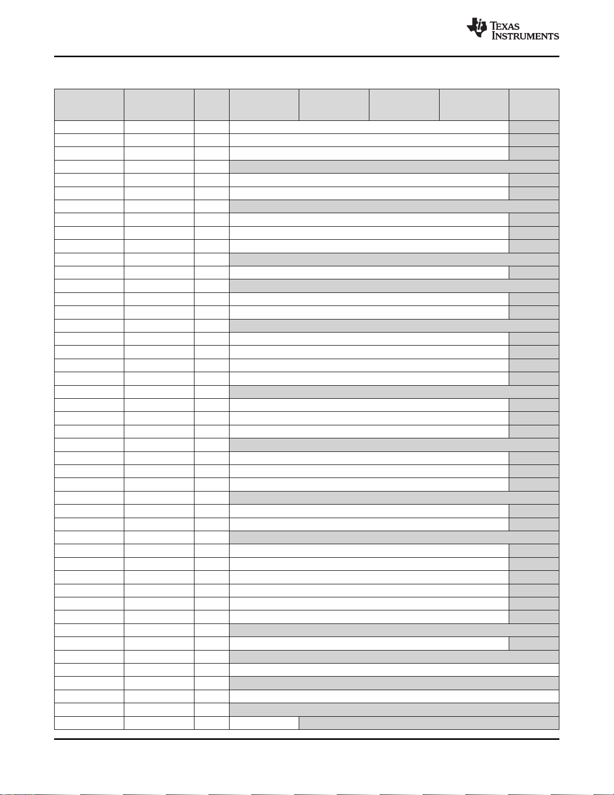
Device Information
PART NUMBER PACKAGE BODY SIZE
AM1806ZCE NFBGA (361) 13,00 mm x 13,00 mm
AM1806ZWT NFBGA (361) 16,00 mm x 16,00 mm
Copyright © 2010–2014, Texas Instruments Incorporated AM1806 ARM Microprocessor 3
Submit Documentation Feedback
Product Folder Links: AM1806
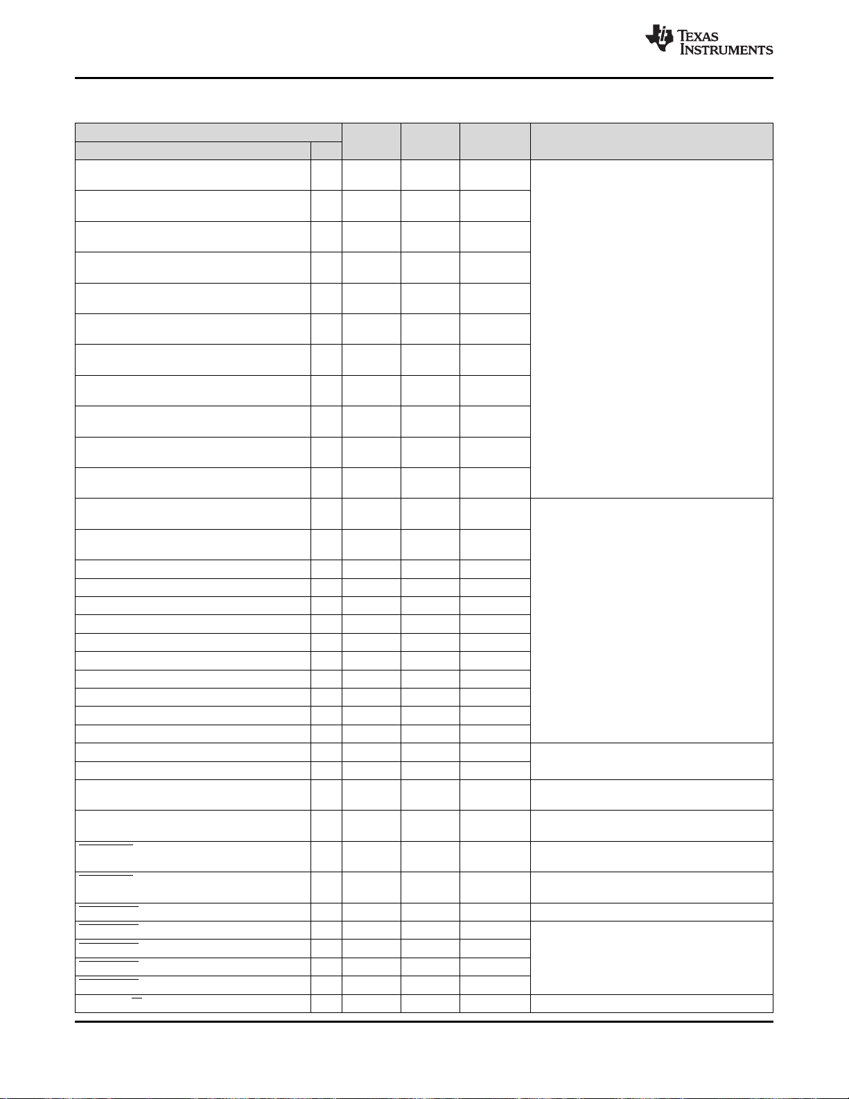
Switched Central Resource (SCR)
16KB
I-Cache
16KB
D-Cache
4KB ETB
ARM926EJ-S CPU
With MMU
ARM Subsystem
JTAG Interface
System Control
Input
Clock(s)
64KB ROM
8KB RAM
(Vector Table)
Power/Sleep
Controller
Pin
Multiplexing
PLL/Clock
Generator
w/OSC
GeneralPurpose
Timer (x3)
Serial Interfaces
Audio Ports
McASP
w/FIFO
DMA
Peripherals
Display Internal Memory
LCD
Ctlr
128KB
RAM
External Memory InterfacesConnectivity
EDMA3
(x2)
Control Timers
ePWM
(x2)
eCAP
(x3)
EMIFA(8b/16B)
NAND/Flash
16b SDRAM
DDR2/MDDR
Controller
RTC/
32-kHz
OSC
I C
(x2)
2
SPI
(x2)
UART
(x3)
McBSP
(x2)
Video
VPIF
Parallel Port
uPP
USB2.0
OTG Ctlr
PHY
HPI
MMC/SD
(8b)
(x2)
Customizable Interface
PRU Subsystem
Memory
Protection
AM1806
SPRS658F –FEBRUARY 2010–REVISED MARCH 2014
1.4 Functional Block Diagram
Figure 1-1 shows the functional block diagram of the device.
www.ti.com
(1) Note: Not all peripherals are available at the same time due to multiplexing.
Figure 1-1. Functional Block Diagram
4 AM1806 ARM Microprocessor Copyright © 2010–2014, Texas Instruments Incorporated
Submit Documentation Feedback
Product Folder Links: AM1806

AM1806
www.ti.com
SPRS658F –FEBRUARY 2010–REVISED MARCH 2014
Table of Contents
1 AM1806 ARM Microprocessor......................... 1 6.8 Power and Sleep Controller (PSC).................. 82
1.1 Features .............................................. 1 6.9 EDMA ............................................... 87
1.2 Applications........................................... 2 6.10 External Memory Interface A (EMIFA) .............. 93
1.3 Description............................................ 3 6.11 DDR2/mDDR Memory Controller .................. 104
1.4 Functional Block Diagram ............................ 4 6.12 Memory Protection Units .......................... 117
2 Revision History ......................................... 6 6.13 MMC / SD / SDIO (MMCSD0, MMCSD1) ......... 120
3 Device Overview ......................................... 7 6.14 Multichannel Audio Serial Port (McASP) .......... 123
3.1 Device Characteristics................................ 7 6.15 Multichannel Buffered Serial Port (McBSP)........ 132
3.2 Device Compatibility.................................. 8 6.16 Serial Peripheral Interface Ports (SPI0, SPI1)..... 141
3.3 ARM Subsystem...................................... 8 6.17 Inter-Integrated Circuit Serial Ports (I2C) .......... 162
3.4 Memory Map Summary ............................. 11
3.5 Pin Assignments .................................... 14
3.6 Pin Multiplexing Control............................. 17
3.7 Terminal Functions .................................. 18
3.8 Unused Pin Configurations.......................... 54
4 Device Configuration.................................. 55
4.1 Boot Modes ......................................... 55
4.2 SYSCFG Module.................................... 55
4.3 Pullup/Pulldown Resistors .......................... 58
5 Specifications........................................... 59
5.1 Absolute Maximum Ratings Over Operating
Junction Temperature Range
(Unless Otherwise Noted) ................................. 59
5.2 Handling Ratings.................................... 59
5.3 Recommended Operating Conditions............... 60
5.4 Notes on Recommended Power-On Hours (POH) . 62
5.5 Electrical Characteristics Over Recommended
Ranges of Supply Voltage and Operating Junction
Temperature (Unless Otherwise Noted) ............ 63 7.1 Device Support..................................... 236
6 Peripheral Information and Electrical 7.2 Documentation Support............................ 237
Specifications........................................... 64
6.1 Parameter Information .............................. 64
6.2 Recommended Clock and Control Signal Transition
Behavior............................................. 65
6.3 Power Supplies...................................... 65
6.4 Reset ................................................ 66
6.5 Crystal Oscillator or External Clock Input........... 70
6.6 Clock PLLs .......................................... 71
6.7 Interrupts ............................................ 76
6.18 Universal Asynchronous Receiver/Transmitter
(UART)............................................. 166
6.19 Universal Serial Bus OTG Controller (USB0)
[USB2.0 OTG] ..................................... 168
6.20 LCD Controller (LCDC) ............................ 175
6.21 Host-Port Interface (UHPI)......................... 190
6.22 Universal Parallel Port (uPP) ...................... 198
6.23 Video Port Interface (VPIF) ........................ 203
6.24 Enhanced Capture (eCAP) Peripheral............. 208
6.25 Enhanced High-Resolution Pulse-Width Modulator
(eHRPWM)......................................... 211
6.26 Timers.............................................. 216
6.27 Real Time Clock (RTC) ............................ 218
6.28 General-Purpose Input/Output (GPIO)............. 221
6.29 Programmable Real-Time Unit Subsystem (PRUSS)
..................................................... 225
6.30 Emulation Logic .................................... 228
7 Device and Documentation Support.............. 236
7.3 Community Resources............................. 237
7.4 Trademarks ........................................ 237
7.5 Electrostatic Discharge Caution ................... 238
7.6 Glossary............................................ 238
8 Mechanical Packaging and Orderable
Information............................................. 238
8.1 Thermal Data for ZCE Package ................... 238
8.2 Thermal Data for ZWT Package ................... 239
Copyright © 2010–2014, Texas Instruments Incorporated Table of Contents 5
Submit Documentation Feedback
Product Folder Links: AM1806

AM1806
SPRS658F –FEBRUARY 2010–REVISED MARCH 2014
2 Revision History
NOTE: Page numbers for previous revisions may differ from page numbers in the current version.
This data manual revision history highlights the changes made to the SPRS658E device-specific data
manual to make it an SPRS658F revision.
SEE ADDITIONS/MODIFICATIONS/DELETIONS
• Moved Trademarks information from first page to within Section 7, Device and Documentation
Global
Section 1.3
Description
Section 3.7
Terminal Functions
Section 3.7.17
Universal Serial Bus Modules
(USB0)
Section 3.8
Unused Pin Configurations
Section 5
Specifications
Section 5.4
Notes on Recommended
Power-On Hours
Section 6.10.5 • Added vertical lines to show difference between Setup, Strobe, and Hold
EMIFA Electrical/Timing Figure 6-13, Asynchronous Memory Write Timing for EMIFA:
Section 7.1.2
Device and DevelopmentSupport Tool Nomenclature
Section 7.6
Glossary
Support.
• Moved ESDS Warning to within Section 7, Device and Documentation Support.
• Updated Features, Applications, and Description for consistency and translation.
Added NEW Device Information Table.
Table 3-3 thru Table 3-25:
• Updated/Changed footnote beginning with "IPD = Internal Pulldown resistor..."; added
sentence "For more detailed information on pullup/pulldown..."
Table 3-19, Universal Serial Bus (USB) Terminal Functions
• Updated/Changed the capacitor value in USB0_VDDA12 pin DESCRIPTION from "1 μF" to
"0.22-μF"
Table 3-28, Unused USB0 Signal Configurations:
• Updated/Changed USB0_VDDA12 row text from "No Connect" to "...to an external 0.22-μF
filter capacitor"
Updated/Changed title from "Device Operating Conditions" to "Specifications"
Section 5.2, Handling Ratings:
• Split handling, ratings, and certifications from the Abs Max table and placed in NEW Handling
Ratings table.
Table 5-1, Recommended Power-On Hours:
• Updated/Changed all applicable Silicon Revisions from "B" to "B/E"
Figure 6-12, Asynchronous Memory Read Timing for EMIFA:
• Added vertical lines to show difference between Setup, Strobe, and Hold
Figure 7-1, Device Nomenclature:
• Added "E = Silicon Revision 2.3" under SILICON REVISION
Added NEW section.
www.ti.com
Revision History
6 Revision History Copyright © 2010–2014, Texas Instruments Incorporated
Submit Documentation Feedback
Product Folder Links: AM1806
AM1806
www.ti.com
SPRS658F –FEBRUARY 2010–REVISED MARCH 2014
3 Device Overview
3.1 Device Characteristics
Table 3-1 provides an overview of the device. The table shows significant features of the device, including
the capacity of on-chip RAM, peripherals, and the package type with pin count.
Table 3-1. Characteristics of the Device
HARDWARE FEATURES AM1806
DDR2/mDDR Controller
EMIFA
Flash Card Interface MMC and SD cards supported
EDMA3
Timers
Peripherals
Not all peripherals pins
are available at the
same time (for more
detail, see the Device
Configurations section).
On-Chip Memory
JTAG BSDL_ID DEVIDR0 Register 0x0B7D_102F
CPU Frequency MHz ARM926 375 MHz (1.2V) or 456 MHz (1.3V)
Voltage
Packages
Product Status
(1) PRODUCTION DATA information is current as of publication date. Products conform to specifications per the terms of the Texas
Instruments standard warranty. Production processing does not necessarily include testing of all parameters.
(1)
UART 3 (each with RTS and CTS flow control)
SPI 2 (Each with one hardware chip select)
I2C 2 (both Master/Slave)
Multichannel Audio Serial Port [McASP] 1 (each with transmit/receive, FIFO buffer, 16 serializers)
Multichannel Buffered Serial Port [McBSP] 2 (each with transmit/receive, FIFO buffer, 16)
eHRPWM
USB 2.0 (USB0) High-Speed OTG Controller with on-chip OTG PHY
General-Purpose Input/Output Port 9 banks of 16-bit
LCD Controller 1
Universal Parallel Port (uPP) 1
Video Port Interface (VPIF) 1 (video in and video out)
PRU Subsystem (PRUSS) 2 Programmable PRU Cores
Size (Bytes) 168KB RAM
Organization 8KB RAM (Vector Table)
Core (V)
I/O (V) 1.8V or 3.3 V
Product Preview (PP),
Advance Information (AI),
or Production Data (PD)
4 64-Bit General Purpose (each configurable as 2 separate
DDR2, 16-bit bus width, up to 156 MHz
Mobile DDR, 16-bit bus width, up to 150 MHz
Asynchronous (8/16-bit bus width) RAM, Flash,
16-bit SDRAM, NOR, NAND
64 independent channels, 16 QDMA channels,
2 channel controllers, 3 transfer controllers
32-bit timers, one configurable as Watch Dog)
4 Single Edge, 4 Dual Edge Symmetric, or
2 Dual Edge Asymmetric Outputs
ARM
16KB I-Cache
16KB D-Cache
64KB ROM
ADDITIONAL MEMORY
128KB RAM
1.2 V nominal for 375 MHz version
1.3 V nominal for 456 MHz version
13 mm x 13 mm, 361-Ball 0.65 mm pitch, PBGA (ZCE)
16 mm x 16 mm, 361-Ball 0.80 mm pitch, PBGA (ZWT)
375 MHz versions - PD
456 MHz versions - PD
Copyright © 2010–2014, Texas Instruments Incorporated Device Overview 7
Submit Documentation Feedback
Product Folder Links: AM1806

AM1806
SPRS658F –FEBRUARY 2010–REVISED MARCH 2014
3.2 Device Compatibility
The ARM926EJ-S RISC CPU is compatible with other ARM9 CPUs from ARM Holdings plc.
3.3 ARM Subsystem
The ARM Subsystem includes the following features:
• ARM926EJ-S RISC processor
• ARMv5TEJ (32/16-bit) instruction set
• Little endian
• System Control Co-Processor 15 (CP15)
• MMU
• 16KB Instruction cache
• 16KB Data cache
• Write Buffer
• Embedded Trace Module and Embedded Trace Buffer (ETM/ETB)
• ARM Interrupt controller
3.3.1 ARM926EJ-S RISC CPU
www.ti.com
The ARM Subsystem integrates the ARM926EJ-S processor. The ARM926EJ-S processor is a member of
ARM9 family of general-purpose microprocessors. This processor is targeted at multi-tasking applications
where full memory management, high performance, low die size, and low power are all important. The
ARM926EJ-S processor supports the 32-bit ARM and 16 bit THUMB instruction sets, enabling the user to
trade off between high performance and high code density. Specifically, the ARM926EJ-S processor
supports the ARMv5TEJ instruction set, which includes features for efficient execution of Java byte codes,
providing Java performance similar to Just in Time (JIT) Java interpreter, but without associated code
overhead.
The ARM926EJ-S processor supports the ARM debug architecture and includes logic to assist in both
hardware and software debug. The ARM926EJ-S processor has a Harvard architecture and provides a
complete high performance subsystem, including:
• ARM926EJ -S integer core
• CP15 system control coprocessor
• Memory Management Unit (MMU)
• Separate instruction and data caches
• Write buffer
• Separate instruction and data (internal RAM) interfaces
• Separate instruction and data AHB bus interfaces
• Embedded Trace Module and Embedded Trace Buffer (ETM/ETB)
For more complete details on the ARM9, refer to the ARM926EJ-S Technical Reference Manual, available
at http://www.arm.com
3.3.2 CP15
The ARM926EJ-S system control coprocessor (CP15) is used to configure and control instruction and
data caches, Memory Management Unit (MMU), and other ARM subsystem functions. The CP15 registers
are programmed using the MRC and MCR ARM instructions, when the ARM in a privileged mode such as
supervisor or system mode.
8 Device Overview Copyright © 2010–2014, Texas Instruments Incorporated
Submit Documentation Feedback
Product Folder Links: AM1806

www.ti.com
3.3.3 MMU
A single set of two level page tables stored in main memory is used to control the address translation,
permission checks and memory region attributes for both data and instruction accesses. The MMU uses a
single unified Translation Lookaside Buffer (TLB) to cache the information held in the page tables. The
MMU features are:
• Standard ARM architecture v4 and v5 MMU mapping sizes, domains and access protection scheme.
• Mapping sizes are:
– 1MB (sections)
– 64KB (large pages)
– 4KB (small pages)
– 1KB (tiny pages)
• Access permissions for large pages and small pages can be specified separately for each quarter of
the page (subpage permissions)
• Hardware page table walks
• Invalidate entire TLB, using CP15 register 8
• Invalidate TLB entry, selected by MVA, using CP15 register 8
• Lockdown of TLB entries, using CP15 register 10
3.3.4 Caches and Write Buffer
AM1806
SPRS658F –FEBRUARY 2010–REVISED MARCH 2014
The size of the Instruction cache is 16KB, Data cache is 16KB. Additionally, the caches have the following
features:
• Virtual index, virtual tag, and addressed using the Modified Virtual Address (MVA)
• Four-way set associative, with a cache line length of eight words per line (32-bytes per line) and with
two dirty bits in the Dcache
• Dcache supports write-through and write-back (or copy back) cache operation, selected by memory
region using the C and B bits in the MMU translation tables
• Critical-word first cache refilling
• Cache lockdown registers enable control over which cache ways are used for allocation on a line fill,
providing a mechanism for both lockdown, and controlling cache corruption
• Dcache stores the Physical Address TAG (PA TAG) corresponding to each Dcache entry in the TAG
RAM for use during the cache line write-backs, in addition to the Virtual Address TAG stored in the
TAG RAM. This means that the MMU is not involved in Dcache write-back operations, removing the
possibility of TLB misses related to the write-back address.
• Cache maintenance operations provide efficient invalidation of, the entire Dcache or Icache, regions of
the Dcache or Icache, and regions of virtual memory.
The write buffer is used for all writes to a noncachable bufferable region, write-through region and write
misses to a write-back region. A separate buffer is incorporated in the Dcache for holding write-back for
cache line evictions or cleaning of dirty cache lines. The main write buffer has 16-word data buffer and a
four-address buffer. The Dcache write-back has eight data word entries and a single address entry.
3.3.5 Advanced High-Performance Bus (AHB)
The ARM Subsystem uses the AHB port of the ARM926EJ-S to connect the ARM to the Config bus and
the external memories. Arbiters are employed to arbitrate access to the separate D-AHB and I-AHB by the
Config Bus and the external memories bus.
Copyright © 2010–2014, Texas Instruments Incorporated Device Overview 9
Submit Documentation Feedback
Product Folder Links: AM1806

AM1806
SPRS658F –FEBRUARY 2010–REVISED MARCH 2014
3.3.6 Embedded Trace Macrocell (ETM) and Embedded Trace Buffer (ETB)
To support real-time trace, the ARM926EJ-S processor provides an interface to enable connection of an
Embedded Trace Macrocell (ETM). The ARM926ES-J Subsystem in the device also includes the
Embedded Trace Buffer (ETB). The ETM consists of two parts:
• Trace Port provides real-time trace capability for the ARM9.
• Triggering facilities provide trigger resources, which include address and data comparators, counter,
and sequencers.
The device trace port is not pinned out and is instead only connected to the Embedded Trace Buffer. The
ETB has a 4KB buffer memory. ETB enabled debug tools are required to read/interpret the captured trace
data.
3.3.7 ARM Memory Mapping
By default the ARM has access to most on and off chip memory areas, including EMIFA, DDR2, and the
additional 128K byte on chip SRAM. Likewise almost all of the on chip peripherals are accessible to the
ARM by default.
To improve security and/or robustness, the device has extensive memory and peripheral protection units
which can be configured to limit access rights to the various on/off chip resources to specific hosts;
including the ARM as well as other master peripherals. This allows the system tasks to be partitioned
between the ARM and DSP as best suites the particular application; while enhancing the overall
robustness of the solution.
www.ti.com
See Table 3-2 for a detailed top level device memory map that includes the ARM memory space.
10 Device Overview Copyright © 2010–2014, Texas Instruments Incorporated
Submit Documentation Feedback
Product Folder Links: AM1806
AM1806
www.ti.com
SPRS658F –FEBRUARY 2010–REVISED MARCH 2014
3.4 Memory Map Summary
Note: Read/Write accesses to illegal or reserved addresses in the memory map may cause undefined
behavior.
Table 3-2. Device Top Level Memory Map
Start Address End Address Size ARM Mem Map EDMA Mem Map PRUSS Mem Master LCDC Mem
0x0000 0000 0x0000 0FFF 4K PRUSS Local
0x0000 1000 0x01BB FFFF
0x01BC 0000 0x01BC 0FFF 4K ARM ETB
memory
0x01BC 1000 0x01BC 17FF 2K ARM ETB reg
0x01BC 1800 0x01BC 18FF 256 ARM Ice Crusher
0x01BC 1900 0x01BF FFFF
0x01C0 0000 0x01C0 7FFF 32K EDMA3 CC
0x01C0 8000 0x01C0 83FF 1K EDMA3 TC0
0x01C0 8400 0x01C0 87FF 1K EDMA3 TC1
0x01C0 8800 0x01C0 FFFF
0x01C1 0000 0x01C1 0FFF 4K PSC 0
0x01C1 1000 0x01C1 1FFF 4K PLL Controller 0
0x01C1 2000 0x01C1 3FFF
0x01C1 4000 0x01C1 4FFF 4K SYSCFG0
0x01C1 5000 0x01C1 FFFF
0x01C2 0000 0x01C2 0FFF 4K Timer0
0x01C2 1000 0x01C2 1FFF 4K Timer1
0x01C2 2000 0x01C2 2FFF 4K I2C 0
0x01C2 3000 0x01C2 3FFF 4K RTC
0x01C2 4000 0x01C3 FFFF
0x01C4 0000 0x01C4 0FFF 4K MMC/SD 0
0x01C4 1000 0x01C4 1FFF 4K SPI 0
0x01C4 2000 0x01C4 2FFF 4K UART 0
0x01C4 3000 0x01CF FFFF
0x01D0 0000 0x01D0 0FFF 4K McASP 0 Control
0x01D0 1000 0x01D0 1FFF 4K McASP 0 AFIFO Ctrl
0x01D0 2000 0x01D0 2FFF 4K McASP 0 Data
0x01D0 3000 0x01D0 BFFF
0x01D0 C000 0x01D0 CFFF 4K UART 1
0x01D0 D000 0x01D0 DFFF 4K UART 2
0x01D0 E000 0x01D0 FFFF
0x01D1 0000 0x01D1 07FF 2K McBSP0
0x01D1 0800 0x01D1 0FFF 2K McBSP0 FIFO Ctrl
0x01D1 1000 0x01D1 17FF 2K McBSP1
0x01D1 1800 0x01D1 1FFF 2K McBSP1 FIFO Ctrl
0x01D1 2000 0x01DF FFFF
0x01E0 0000 0x01E0 FFFF 64K USB0
0x01E1 0000 0x01E1 0FFF 4K UHPI
0x01E1 1000 0x01E1 2FFF
0x01E1 3000 0x01E1 3FFF 4K LCD Controller
0x01E1 4000 0x01E1 4FFF 4K Memory Protection Unit 1 (MPU 1)
Map Peripheral Mem Map
Map
Address Space
Copyright © 2010–2014, Texas Instruments Incorporated Device Overview 11
Submit Documentation Feedback
Product Folder Links: AM1806
AM1806
SPRS658F –FEBRUARY 2010–REVISED MARCH 2014
www.ti.com
Table 3-2. Device Top Level Memory Map (continued)
Start Address End Address Size ARM Mem Map EDMA Mem Map PRUSS Mem Master LCDC Mem
0x01E1 5000 0x01E1 5FFF 4K Memory Protection Unit 2 (MPU 2)
0x01E1 6000 0x01E1 6FFF 4K UPP
0x01E1 7000 0x01E1 7FFF 4K VPIF
0x01E1 8000 0x01E1 9FFF
0x01E1 A000 0x01E1 AFFF 4K PLL Controller 1
0x01E1 B000 0x01E1 BFFF 4K MMCSD1
0x01E1 C000 0x01E2 5FFF
0x01E2 6000 0x01E2 6FFF 4K GPIO
0x01E2 7000 0x01E2 7FFF 4K PSC 1
0x01E2 8000 0x01E2 8FFF 4K I2C 1
0x01E2 9000 0x01E2 BFFF
0x01E2 C000 0x01E2 CFFF 4K SYSCFG1
0x01E2 D000 0x01E2 FFFF
0x01E3 0000 0x01E3 7FFF 32K EDMA3 CC1
0x01E3 8000 0x01E3 83FF 1K EDMA3 TC2
0x01E3 8400 0x01EF FFFF
0x01F0 0000 0x01F0 0FFF 4K eHRPWM 0
0x01F0 1000 0x01F0 1FFF 4K HRPWM 0
0x01F0 2000 0x01F0 2FFF 4K eHRPWM 1
0x01F0 3000 0x01F0 3FFF 4K HRPWM 1
0x01F0 4000 0x01F0 5FFF
0x01F0 6000 0x01F0 6FFF 4K ECAP 0
0x01F0 7000 0x01F0 7FFF 4K ECAP 1
0x01F0 8000 0x01F0 8FFF 4K ECAP 2
0x01F0 9000 0x01F0 BFFF
0x01F0 C000 0x01F0 CFFF 4K Timer2
0x01F0 D000 0x01F0 DFFF 4K Timer3
0x01F0 E000 0x01F0 EFFF 4K SPI1
0x01F0 F000 0x01F0 FFFF
0x01F1 0000 0x01F1 0FFF 4K McBSP0 FIFO Data
0x01F1 1000 0x01F1 1FFF 4K McBSP1 FIFO Data
0x01F1 2000 0x3FFF FFFF
0x4000 0000 0x5FFF FFFF 512M EMIFA SDRAM data (CS0)
0x6000 0000 0x61FF FFFF 32M EMIFA async data (CS2)
0x6200 0000 0x63FF FFFF 32M EMIFA async data (CS3)
0x6400 0000 0x65FF FFFF 32M EMIFA async data (CS4)
0x6600 0000 0x67FF FFFF 32M EMIFA async data (CS5)
0x6800 0000 0x6800 7FFF 32K EMIFA Control Regs
0x6800 8000 0x7FFF FFFF
0x8000 0000 0x8001 FFFF 128K On-Chip RAM
0x8002 0000 0xAFFF FFFF
0xB000 0000 0xB000 7FFF 32K DDR2/mDDR Control Regs
0xB000 8000 0xBFFF FFFF
0xC000 0000 0xCFFF FFFF 256M DDR2/mDDR Data
0xD000 0000 0xE000 0000
0xFFFD 0000 0xFFFD FFFF 64K ARM local ROM
Map Peripheral Mem Map
Map
12 Device Overview Copyright © 2010–2014, Texas Instruments Incorporated
Submit Documentation Feedback
Product Folder Links: AM1806
AM1806
www.ti.com
SPRS658F –FEBRUARY 2010–REVISED MARCH 2014
Table 3-2. Device Top Level Memory Map (continued)
Start Address End Address Size ARM Mem Map EDMA Mem Map PRUSS Mem Master LCDC Mem
0xFFFE 0000 0xFFFE DFFF
0xFFFE E000 0xFFFE FFFF 8K ARM Interrupt
Controller
0xFFFF 0000 0xFFFF 1FFF 8K ARM local RAM ARM Local RAM
0xFFFF 2000 0xFFFF FFFF
Map Peripheral Mem Map
Map
(PRU0 only)
Copyright © 2010–2014, Texas Instruments Incorporated Device Overview 13
Submit Documentation Feedback
Product Folder Links: AM1806
W
V
U
T
R
P
N
M
L
K
10987654321
10987654321
DVDD3318_C
VP_CLKOUT3/
PRU1_R30[0]/
GP6[1]/
PRU1_R31[1]
V
SS
NC
VP_CLKOUT2/
MMCSD1_DAT[2]/
PRU1_R30[2]/
GP6[3]/
PRU1_R31[3]
NC
NC
NC NCNC NC
NC NCNC
DVDD3318_C
DDR_A[11]
VP_DOUT[15]/
LCD_D[15]/
UPP_XD[7]/
GP7[7]/
BOOT[7]
DV
DD3318_C
DV
DD18
DDR_DVDD18 DDR_DVDD18
DDR_D[15]
DDR_RAS
DDR_CLKP
DDR_CLKN
DDR_A[2]DDR_A[10]
V
SS
LCD_AC_ENB_CS/
GP6[0]/
PRU1_R31[28]
DDR_A[13]
DDR_CAS
DDR_A[5]
DDR_CKE
DDR_BA[0]
V
SS
CV
DD
RV
DD
DDR_A[9] DDR_A[1]
DDR_WE
DDR_D[10]
DDR_A[7]
DDR_A[0] DDR_D[12]
DDR_A[12] DDR_A[3]
DDR_CS
DDR_A[6]
DDR_DQM[1]
V
SS
CV
DD
V
SS
DDR_DVDD18
VP_DOUT[12]/
LCD_D[12]/
UPP_XD[4]/
GP7[4]/
BOOT[4]
DDR_VREF
DDR_BA[1]
DDR_A[8]
DDR_A[4]
DDR_BA[2]
V
SS
W
V
U
T
R
P
N
M
L
K
DDR_D[13]
V
SS
V
SS
V
SS
V
SS
DV
DD18
V
SS
V
SS
V
SS
V
SS
NC
V
SS
V
SS
V
SS
V
SS
CV
DD
CV
DD
V
SS
DDR_DVDD18DDR_DVDD18DDR_DVDD18DDR_DVDD18
DVDD3318_C
VP_DOUT[13]/
LCD_D[13]/
UPP_XD[5]/
GP7[5]/
BOOT[5]
VP_DOUT[14]/
LCD_D[14]/
UPP_XD[6]/
GP7[6]/
BOOT[6]
DDR_DVDD18 DDR_DVDD18 DDR_DVDD18
VP_DOUT[9]/
LCD_D[9]/
UPP_XD[1]/
GP7[1]/
BOOT[1]
VP_DOUT[10]/
LCD_D[10]/
UPP_XD[2]/
GP7[2]/
BOOT[2]
VP_DOUT[11]/
LCD_D[11]/
UPP_XD[3]/
GP7[3]/
BOOT[3]
VP_DOUT[6]/
LCD_D[6]/
UPP_XD[14]/
GP7[14]/
PRU1_R31[14]
VP_DOUT[7]/
LCD_D[7]/
UPP_XD[15]/
GP7[15]/
PRU1_R31[15]
VP_DOUT[8]/
LCD_D[8]/
UPP_XD[0]/
GP7[0]/
BOOT[0]
VP_DOUT[3]/
LCD_D[3]/
UPP_XD[11]/
GP7[11]/
PRU1_R31[11]
VP_DOUT[4]/
LCD_D[4]/
UPP_XD[12]/
GP7[12]/
PRU1_R31[12]
VP_DOUT[5]/
LCD_D[5]/
UPP_XD[13]/
GP7[13]/
PRU1_R31[13]
VP_DOUT[0]/
LCD_D[0]/
UPP_XD[8]/
GP7[8]/
PRU1_R31[8]
VP_DOUT[1]/
LCD_D[1]/
UPP_XD[9]/
GP7[9]/
PRU1_R31[9]
VP_DOUT[2]/
LCD_D[2]/
UPP_XD[10]/
GP7[10]/
PRU1_R31[10]
A B
CD
AM1806
SPRS658F –FEBRUARY 2010–REVISED MARCH 2014
3.5 Pin Assignments
Extensive use of pin multiplexing is used to accommodate the largest number of peripheral functions in
the smallest possible package. Pin multiplexing is controlled using a combination of hardware
configuration at device reset and software programmable register settings.
3.5.1 Pin Map (Bottom View)
The following graphics show the bottom view of the ZCE and ZWT packages pin assignments in four
quadrants (A, B, C, and D). The pin assignments for both packages are identical.
www.ti.com
Figure 3-1. Pin Map (Quad A)
14 Device Overview Copyright © 2010–2014, Texas Instruments Incorporated
Submit Documentation Feedback
Product Folder Links: AM1806
W
V
U
T
R
P
N
M
L
K
191817161514131211
191817161514131211
NC
DVDD3318_C
CV
DD
USB_CVDD
DVDD3318_C
DDR_DQGATE0
DVDD18
DDR_DQGATE1
DDR_D[9] DDR_D[8]DDR_D[11]
DVDD18
RTC_CVDD
RESET
USB0_DM USB0_DP
VP_DIN[11]/
UHPI_HD[3]/
UPP_D[3]/
PRU0_R30[11]/
PRU0_R31[11]
USB0_VDDA33 USB0_VBUS
NC
VP_DIN[0]/
UHPI_HD[8]/
UPP_D[8]/
PRU1_R31[29]
VP_DIN[1]/
UHPI_HD[9]/
UPP_D[9]/
PRU0_R31[23]
VP_DIN[2]/
UHPI_HD[10]/
UPP_D[10]/
PRU0_R31[24]
VP_DIN[4]/
UHPI_HD[12]/
UPP_D[12]/
PRU0_R31[26]
PRU0_R30[28]/
UHPI_HCNTL1/
UPP_CHA_START/
GP6[10]
NC
PLL0_VDDA
PRU0_R30[30]/
/
PRU1_R30[11]/
GP6[12]
UHPI_HINT
USB0_VDDA18
VP_DIN[5]/
UHPI_HD[13]/
UPP_D[13]/
PRU0_R31[27]
DDR_D[1]
VP_DIN[7]/
UHPI_HD[15]/
UPP_D[15]/
PRU0_R31[29]
OSCVSS
DDR_D[2]
VP_DIN[6]/
UHPI_HD[14]/
UPP_D[14]/
PRU0_R31[28]
VP_DIN[3]/
UHPI_HD[11]/
UPP_D[11]/
PRU0_R31[25]
VP_DIN[14]_
HSYNC/
UHPI_HD[6]/
UPP_D[6]/
PRU0_R30[14]/
PRU0_R31[14]
EMU1
VP_DIN[8]/
UHPI_HD[0]/
UPP_D[0]/
GP6[5]/
PRU1_R31[0]
USB0_VDDA12
TDI
NC
PRU0_R30[26]/
UHPI_HR /
UPP_CHA_WAIT/
GP6[8]/
PRU1_R31[17]
W
VP_DIN[12]/
UHPI_HD[4]/
UPP_D[4]/
PRU0_R30[12]/
PRU0_R31[12]
RESETOUT
UHPI_HAS//
PRU1_R30[14]/
GP6[15]
RSV2
RTCK/
GP8[0]
OSCOUT
DDR_D[0]
PRU0_R30[27]/
UHPI_HHWIL/
UPP_CHA_ENABLE/
GP6[9]
VP_DIN[13]_
FIELD/
UHPI_HD[5]/
UPP_D[5]/
PRU0_R30[13]/
PRU0_R31[13]
TRST
OSCIN
VP_CLKIN1/
/
PRU1_R30[9]/
GP6[6]/
PRU1_R31[16]
UHPI_HDS1
VP_DIN[15]_
VSYNC/
UHPI_HD[7]/
UPP_D[7]/
PRU0_R30[15]/
PRU0_R31[15]
VP_CLKIN0/
/
PRU1_R30[10]/
GP6[7]/
UPP_2xTXCLK
UHPI_HCS
VP_DIN[10]/
UHPI_HD[2]/
UPP_D[2]/
PRU0_R30[10]/
PRU0_R31[10]
V
SS
DVDD3318_B
PLL0_VSSA
TMS
PRU0_R30[31]/
/
PRU1_R30[12]
GP6[13]
UHPI_HRDY
NC
PLL1_VSSA
PLL1_VDDA
NC
USB0_ID
VP_DIN[9]/
UHPI_HD[1]/
UPP_D[1]/
PRU0_R30[9]/
PRU0_R31[9]
CLKOUT/
/
PRU1_R30[13]/
GP6[14]
UHPI_HDS2
USB0_DRVVBUS
DDR_DQS[0]
PRU0_R30[29]/
UHPI_HCNTL0/
UPP_CHA_CLOCK/
GP6[11]
W
V
U
T
R
P
N
M
L
K
DDR_DQM[0]
DDR_D[3]
DDR_D[4]
DDR_D[6]
DDR_ZP
DDR_D[5]
DDR_D[7]
DDR_D[14]
DDR_DQS[1]
V
SS
V
SS
V
SS
V
SS
V
SS
CV
DD
DVDD3318_C
DVDD3318_C
DVDD3318_C
A B
CD
www.ti.com
AM1806
SPRS658F –FEBRUARY 2010–REVISED MARCH 2014
Figure 3-2. Pin Map (Quad B)
Copyright © 2010–2014, Texas Instruments Incorporated Device Overview 15
Submit Documentation Feedback
Product Folder Links: AM1806
H
G
F
E
D
C
B
A
191817161514131211
191817161514131211
CV
DD
EMA_A[8]/
PRU1_R30[16]/
GP5[8]
EMA_A[14]/
MMCSD0_DAT[7]/
PRU1_R30[22]/
GP5[14]/
PRU1_R31[22]
EMA_A[15]/
MMCSD0_DAT[6]/
PRU1_R30[23]/
GP5[15]/
PRU1_R31[23]
EMA_A[10]/
PRU1_R30[18]/
GP5[10]/
PRU1_R31[18]
EMA_A[9]/
PRU1_R30[17]/
GP5[9]
EMA_A[13]/
PRU0_R30[21]/
PRU1_R30[21]
GP5[13]/
PRU1_R31[21]
EMA_A[12]/
PRU1_R30[20]/
GP5[12]/
PRU1_R31[20]
EMA_A[16]/
MMCSD0_DAT[5]/
PRU1_R30[24]/
GP4[0]
EMA_A[18]/
MMCSD0_DAT[3]/
PRU1_R30[26]/
GP4[2]
DV
DD3318_B
DV
DD18
EMA_A[6]/
GP5[6]
EMA_A[5]/
GP5[5]
EMA_A[2]/
GP5[2]
EMA_A[7]/
PRU1_R30[15]/
GP5[7]
EMA_A[4]/
GP5[4]
SPI0_SIMO/
EPWMSYNCO/
GP8[5]
SPI0_SCS[5]/
UART0_RXD/
GP8[4]
SPI1_SCS[1]/
EPWM1A/
PRU0_R30[8]/
GP2[15]/
TM64P2_IN12
SPI0_SCS[4]/
UART0_TXD/
GP8[3]
SPI0_CLK/
EPWM0A/
GP1[8]
SPI1_SCS[3]/
UART1_RXD/
GP1[1]
SPI1_SCS[0]/
EPWM1B/
PRU0_R30[7]/
GP2[14]/
TM64P3_IN12
EMA_OE/
GP3[10]
SPI1_SCS[4]/
UART2_TXD/
I2C1_SDA/
GP1[2]
EMA_A[3]/
GP5[3]
DV
DD18
RTC_VSS
EMA_WAIT[0]/
PRU0_R30[0]/
GP3[8]/
PRU0_R31[0]
EMA_RAS/
PRU0_R30[3]/
GP2[5]/
PRU0_R31[3]
SPI0_SCS[3]
UART0_CTS//
GP8[2]
SPI0_SCS[0]/
TM64P1_OUT12/
GP1[6]/
TM64P1_IN12
SPI0_SOMI/
EPWMSYNCI/
GP8[6]
SPI0_SCS[2]
UART0_RTS//
GP8[1]
SPI1_SCS[7]/
I2C0_SCL/
TM64P2_OUT12/
GP1[5]
SPI1_SIMO/
GP2[10]
SPI1_CLK/
GP2[13]
EMA_CS[3]/
GP3[14]
V
SS
V
SS
SPI1_ENA/
GP2[12]
RTC_XO
EMA_CS[2]/
GP3[15]
EMA_WAIT[1]/
PRU0_R30[1]/
GP2[1]/
PRU0_R31[1]
EMA_A[20]/
MMCSD0_DAT[1]/
PRU1_R30[28]/
GP4[4]
EMA_BA[1]/
GP2[9]
SPI0_ENA/
EPWM0B/
PRU0_R30[6]
EMA_CS[5]/
GP3[12]
SPI1_SCS[5]/
UART2_RXD/
I2C1_SCL/
GP1[3]
EMA_A[0]/
GP5[0]
EMA_BA[0]/
GP2[8]
EMA_A[1]/
GP5[1]
DV
DD3318_B
SPI0_SCS[1]/
TM64P0_OUT12/
GP1[7]/
TM64P0_IN12
DV
DD3318_A
SPI1_SCS[6]/
I2C0_SDA/
TM64P3_OUT12/
GP1[4]
EMA_CS[0]/
GP2[0]
CV
DD
SPI1_SOMI/
GP2[11]
H
G
F
E
D
C
B
A
J
TDO
TCK
EMU0
RTC_XI
RSVDN
J
SPI1_SCS[2]/
UART1_TXD/
GP1[0]
EMA_A[11]/
PRU1_R30[19]/
GP5[11]/
PRU1_R31[19]
EMA_A[17]/
MMCSD0_DAT[4]/
PRU1_R30[25]
GP4[1]
DV
DD3318_B
DV
DD3318_B
DV
DD18
CV
DD
DV
DD3318_A
DV
DD3318_A
RV
DD
CV
DD
CV
DD
V
SS
CV
DD
DV
DD18
DV
DD3318_B
A B
CD
AM1806
SPRS658F –FEBRUARY 2010–REVISED MARCH 2014
www.ti.com
Figure 3-3. Pin Map (Quad C)
16 Device Overview Copyright © 2010–2014, Texas Instruments Incorporated
Submit Documentation Feedback
Product Folder Links: AM1806
J
H
G
F
E
D
C
B
A
10987654321
10987654321
EMA_D[15]/
GP3[7]
AXR15/
EPWM0TZ[0]/
ECAP2_APWM2/
GP0[7]
ACLKR/
PRU0_R30[20]/
GP0[15]/
PRU0_R31[22]
ACLKX/
PRU0_R30[19]/
GP0[14]/
PRU0_R31[21]
AHCLKX/
USB_REFCLKIN/
/
GP0[10]/
PRU0_R31[17]
UART1_CTS
AFSX/
GP0[12]/
PRU0_R31[19]
AFSR/
GP0[13]/
PRU0_R31[20]
AXR9/
DX1/
GP0[1]
AXR4/
FSR0/
GP1[12]
AXR5/
CLKX0/
GP1[13]
AXR7/
EPWM1TZ[0]/
PRU0_R30[17]
GP1[15]/
PRU0_R31[7]
AXR10/
DR1/
GP0[2]
AXR1/
DX0/
GP1[9]
AXR3/
FSX0/
GP1[11]
AXR2/
DR0/
GP1[10]
MMCSD1_DAT[6]/
LCD_MCLK/
PRU1_R30[6]/
GP8[10]/
PRU1_R31[7]
RTC_ALARM/
/
GP0[8]/
UART2_CTS
DEEPSLEEP
AXR0/
ECAP0_APWM0/
GP8[7]/
CLKS0
PRU0_R30[24]/
MMCSD1_CLK/
UPP_CHB_START/
GP8[14]/
PRU1_R31[26]
MMCSD1_DAT[4]/
LCD_VSYNC/
PRU1_R30[4]/
GP8[8]/
PRU1_R31[5]
V
SS
PRU0_R30[22]/
PRU1_R30[8]/
UPP_CHB_WAIT/
GP8[12]/
PRU1_R31[24]
AXR8/
CLKS1/
ECAP1_APWM1/
GP0[0]/
PRU0_R31[8]
AXR12/
FSR1/
GP0[4]
EMA_D[4]/
GP4[12]
AXR14/
CLKR1/
GP0[6]
EMA_WEN_DQM[1]/
GP2[2]
EMA_D[0]/
GP4[8]
EMA_A[19]/
MMCSD0_DAT[2]/
PRU1_R30[27]/
GP4[3]
EMA_D[9]/
GP3[1]
EMA_A_R /
GP3[9]
W
MMCSD0_CLK/
PRU1_R30[31]/
GP4[7]
EMA_D[8]/
GP3[0]
EMA_D[13]/
GP3[5]
VP_CLKIN2/
MMCSD1_DAT[3]/
PRU1_R30[3]/
GP6[4]/
PRU1_R31[4]
VP_CLKIN3/
MMCSD1_DAT[1]/
PRU1_R30[1]/
GP6[2]/
PRU1_R31[2]
AMUTE/
GP0[9]/
PRU0_R31[16]
PRU0_R30[16]/
UART2_RTS/
DV
DD3318_A
DV
DD3318_A
EMA_WE/
GP3[11]
EMA_D[10]/
GP3[2]
EMA_D[3]/
GP4[11]
EMA_SDCKE/
PRU0_R30[4]/
GP2[6]/
PRU0_R31[4]
EMA_D[14]/
GP3[6]
EMA_D[7]/
GP4[15]
EMA_D[1]/
GP4[9]
EMA_A[22]/
MMCSD0_CMD/
PRU1_R30[30]/
GP4[6]
EMA_D[2]/
GP4[10]
EMA_A[21]/
MMCSD0_DAT[0]/
PRU1_R30[29]/
GP4[5]
PRU0_R30[23]/
MMCSD1_CMD/
UPP_CHB_ENABLE/
GP8[13]/
PRU1_R31[25]
AHCLKR/
/
GP0[11]/
PRU0_R31[18]
PRU0_R30[18]/
UART1_RTS
EMA_D[12]/
GP3[4]
EMA_WEN_DQM[0]/
GP2[3]
EMA_CLK/
PRU0_R30[5]/
GP2[7]/
PRU0_R31[5]
AXR6/
CLKR0/
GP1[14]/
PRU0_R31[6]
AXR11/
FSX1/
GP0[3]
EMA_D[6]/
GP4[14]
EMA_D[11]/
GP3[3]
RV
DD
EMA_D[5]/
GP4[13]
MMCSD1_DAT[7]/
LCD_PCLK/
PRU1_R30[7]/
GP8[11]
MMCSD1_DAT[5]/
LCD_HSYNC/
PRU1_R30[5]/
GP8[9]/
PRU1_R31[6]
PRU0_R30[25]/
MMCSD1_DAT[0]/
UPP_CHB_CLOCK/
GP8[15]/
PRU1_R31[27]
AXR13/
CLKX1/
GP0[5]
J
H
G
F
E
D
C
B
A
EMA_CS[4]/
GP3[13]
EMA_CAS/
PRU0_R30[2]/
GP2[4]/
PRU0_R31[2]
DV
DD3318_B
DV
DD3318_B
DV
DD3318_B
DV
DD3318_B
DV
DD18
CV
DD
CV
DD
DV
DD3318_B
DV
DD18
V
SS
DV
DD3318_A
V
SS
V
SS
CV
DD
CV
DD
V
SS
V
SS
CV
DD
NC NC
DV
DD3318_C
CV
DD
V
SS
V
SS
A B
CD
www.ti.com
AM1806
SPRS658F –FEBRUARY 2010–REVISED MARCH 2014
3.6 Pin Multiplexing Control
Device level pin multiplexing is controlled by registers PINMUX0 - PINMUX19 in the SYSCFG module.
For the device family, pin multiplexing can be controlled on a pin-by-pin basis. Each pin that is multiplexed
with several different functions has a corresponding 4-bit field in one of the PINMUX registers.
Pin multiplexing selects which of several peripheral pin functions controls the pin's IO buffer output data
and output enable values only. The default pin multiplexing control for almost every pin is to select 'none'
of the peripheral functions in which case the pin's IO buffer is held tri-stated.
Note that the input from each pin is always routed to all of the peripherals that share the pin; the PINMUX
registers have no effect on input from a pin.
Figure 3-4. Pin Map (Quad D)
Submit Documentation Feedback
Product Folder Links: AM1806
Copyright © 2010–2014, Texas Instruments Incorporated Device Overview 17
AM1806
SPRS658F –FEBRUARY 2010–REVISED MARCH 2014
3.7 Terminal Functions
Table 3-3 to Table 3-27 identify the external signal names, the associated pin/ball numbers along with the
mechanical package designator, the pin type (I, O, IO, OZ, or PWR), whether the pin/ball has any internal
pullup/pulldown resistors, whether the pin/ball is configurable as an IO in GPIO mode, and a functional pin
description.
3.7.1 Device Reset and JTAG
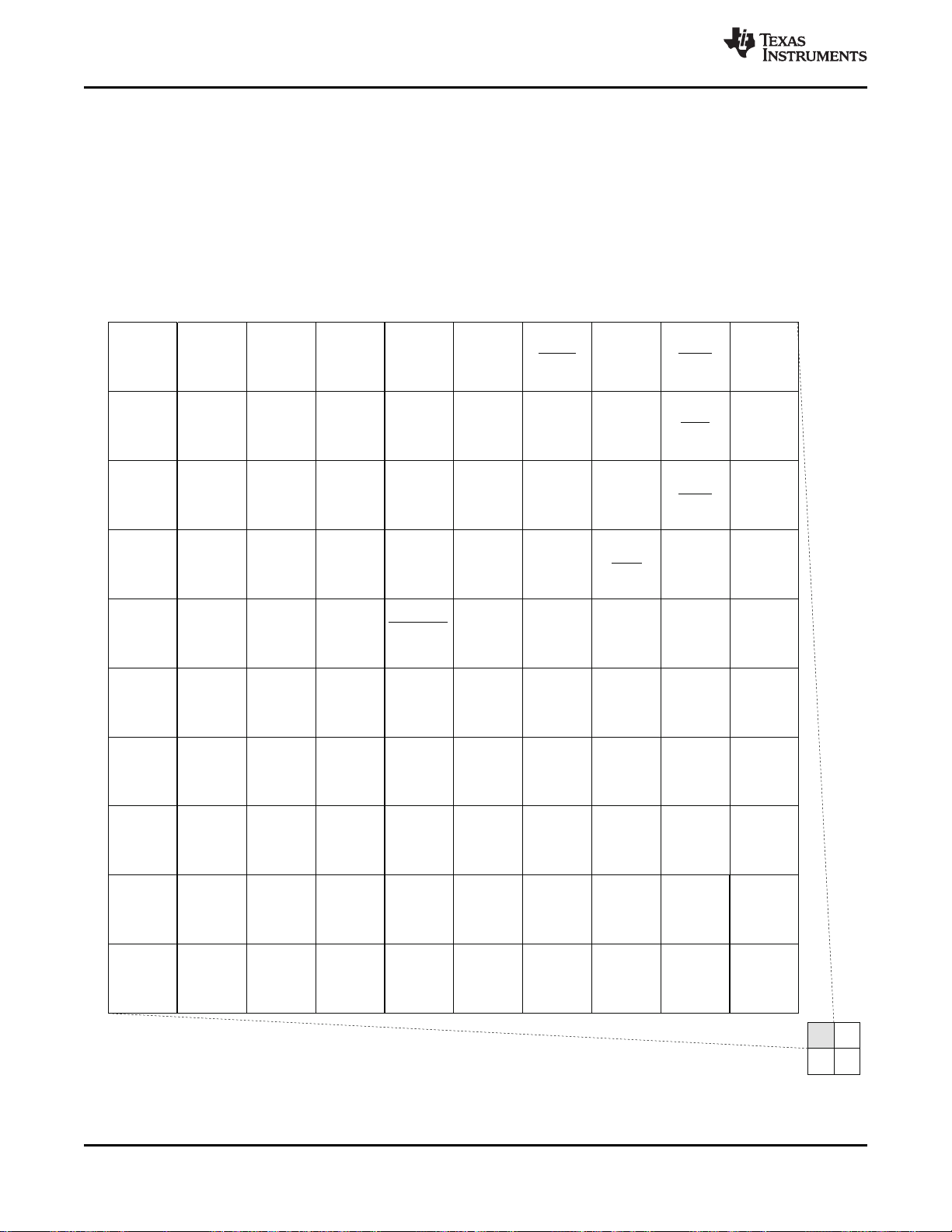
Table 3-3. Reset and JTAG Terminal Functions
www.ti.com
SIGNAL
NAME NO.
RESET K14 I IPU B Device reset input
RESETOUT / UHPI_HAS / PRU1_R30[14] /
GP6[15]
TMS L16 I IPU B JTAG test mode select
TDI M16 I IPU B JTAG test data input
TDO J18 O IPU B JTAG test data output
TCK J15 I IPU B JTAG test clock
TRST L17 I IPD B JTAG test reset
EMU0 J16 I/O IPU B Emulation pin
EMU1 K16 I/O IPU B Emulation pin
RTCK/ GP8[0]
(1) I = Input, O = Output, I/O = Bidirectional, Z = High impedance, PWR = Supply voltage, GND = Ground, A = Analog signal.
Note: For multiplexed pins where functions have different types (ie., input versus output), the table reflects the pin function direction for
that particular peripheral.
(2) IPD = Internal Pulldown resistor, IPU = Internal Pullup resistor. CP[n] = configurable pull-up/pull-down (where n is the pin group) using
the PUPDENA and PUPDSEL registers in the System Module. For more detailed information on pullup/pulldown resistors and situations
where external pullup/pulldown resistors are required, see the Device Configuration section. For electrical specifications on pullup and
internal pulldown circuits, see the Device Operating Conditions section.
(3) This signal is part of a dual-voltage IO group (A, B or C). These groups can be operated at 3.3V or 1.8V nominal. The three groups can
be operated at independent voltages but all pins withina group will operate at the same voltage. Group A operates at the voltage of
power supply DVDD3318_A. Group B operates at the voltage of power supply DVDD3318_B. Group C operates at the voltage of power
supply DVDD3318_C.
(4) Open drain mode for RESETOUT function.
(5) GP8[0] is initially configured as a reserved function after reset and will not be in a predictable state. This signal will only be stable after
the GPIO configuration for this pin has been completed. Users should carefully consider the system implications of this pin being in an
unknown state after reset.
(5)
T17 O
K17 I/O IPD B JTAG Test Clock Return Clock Output
TYPE
(1)
PULL
RESET
(4)
CP[21] C Reset output
JTAG
POWER
(2)
GROUP
(3)
DESCRIPTION
18 Device Overview Copyright © 2010–2014, Texas Instruments Incorporated
Submit Documentation Feedback
Product Folder Links: AM1806
www.ti.com
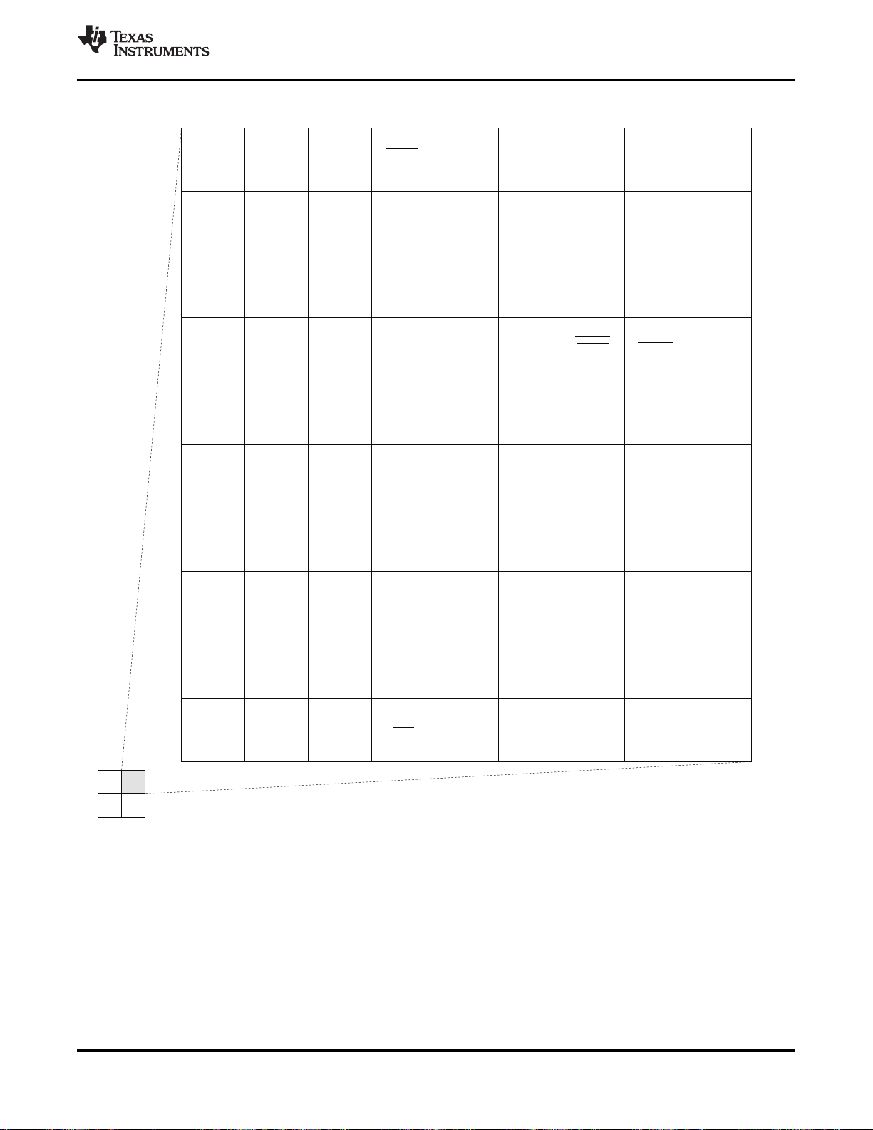
3.7.2 High-Frequency Oscillator and PLL
Table 3-4. High-Frequency Oscillator and PLL Terminal Functions
AM1806
SPRS658F –FEBRUARY 2010–REVISED MARCH 2014
SIGNAL
NAME NO.
CLKOUT / UHPI_HDS2 /
PRU1_R30[13] / GP6[14]
(1)
TYPE
PULL
T18 O CP[22] C PLL Observation Clock
POWER
(2)
GROUP
(3)
DESCRIPTION
1.2-V OSCILLATOR
OSCIN L19 I — — Oscillator input
OSCOUT K19 O — — Oscillator output
OSCVSS L18 GND — — Oscillator ground
1.2-V PLL0
PLL0_VDDA L15 PWR — — PLL analog VDD(1.2-V filtered supply)
PLL0_VSSA M17 GND — — PLL analog VSS(for filter)
1.2-V PLL1
PLL1_VDDA N15 PWR — — PLL analog VDD(1.2-V filtered supply)
PLL1_VSSA M15 GND — — PLL analog VSS(for filter)
(1) I = Input, O = Output, I/O = Bidirectional, Z = High impedance, PWR = Supply voltage, GND = Ground, A = Analog signal.
Note: For multiplexed pins where functions have different types (ie., input versus output), the table reflects the pin function direction for
that particular peripheral.
(2) IPD = Internal Pulldown resistor; IPU = Internal Pullup resistor; CP[n] = configurable pull-up/pull-down (where n is the pin group) using
the PUPDENA and PUPDSEL registers in the System Module. For more detailed information on pullup/pulldown resistors and situations
where external pullup/pulldown resistors are required, see the Device Configuration section. For electrical specifications on pullup and
internal pulldown circuits, see the Device Operating Conditions section.
(3) This signal is part of a dual-voltage IO group (A, B or C). These groups can be operated at 3.3V or 1.8V nominal. The three groups can
be operated at independent voltages but all pins withina group will operate at the same voltage. Group A operates at the voltage of
power supply DVDD3318_A. Group B operates at the voltage of power supply DVDD3318_B. Group C operates at the voltage of power
supply DVDD3318_C.
Copyright © 2010–2014, Texas Instruments Incorporated Device Overview 19
Submit Documentation Feedback
Product Folder Links: AM1806
AM1806
SPRS658F –FEBRUARY 2010–REVISED MARCH 2014
3.7.3 Real-Time Clock and 32-kHz Oscillator
Table 3-5. Real-Time Clock (RTC) and 1.2-V, 32-kHz Oscillator Terminal Functions
www.ti.com
SIGNAL
NAME NO.
TYPE
(1)
PULL
POWER
(2)
GROUP
(3)
DESCRIPTION
RTC_XI J19 I — — RTC 32-kHz oscillator input
RTC_XO H19 O — — RTC 32-kHz oscillator output
RTC_ALARM / UART2_CTS / GP0[8] / DEEPSLEEP F4 O CP[0] A RTC Alarm
RTC_CVDD L14 PWR — —
RTC_V
ss
H18 GND — — Oscillator ground
RTC module core power
(isolated from chip CVDD)
(1) I = Input, O = Output, I/O = Bidirectional, Z = High impedance, PWR = Supply voltage, GND = Ground, A = Analog signal.
Note: For multiplexed pins where functions have different types (ie., input versus output), the table reflects the pin function direction for
that particular peripheral.
(2) IPD = Internal Pulldown resistor; IPU = Internal Pullup resistor; CP[n] = configurable pull-up/pull-down (where n is the pin group) using
the PUPDENA and PUPDSEL registers in the System Module. The pull-up and pull-down control of these pins is not active until the
device is out of reset. During reset, all of the pins associated with these registers are pulled down. If the application requires a pull-up,
an external pull-up can be used. For more detailed information on pullup/pulldown resistors and situations where external
pullup/pulldown resistors are required, see the Device Configuration section. For electrical specifications on pullup and internal pulldown
circuits, see the Device Operating Conditions section.
(3) This signal is part of a dual-voltage IO group (A, B or C). These groups can be operated at 3.3V or 1.8V nominal. The three groups can
be operated at independent voltages but all pins withina group will operate at the same voltage. Group A operates at the voltage of
power supply DVDD3318_A. Group B operates at the voltage of power supply DVDD3318_B. Group C operates at the voltage of power
supply DVDD3318_C.
3.7.4 DEEPSLEEP Power Control
Table 3-6. DEEPSLEEP Power Control Terminal Functions
SIGNAL
NAME NO.
TYPE
(1)
PULL
RTC_ALARM / UART2_CTS / GP0[8] / DEEPSLEEP F4 I CP[0] A DEEPSLEEP power control output
(1) I = Input, O = Output, I/O = Bidirectional, Z = High impedance, PWR = Supply voltage, GND = Ground, A = Analog signal.
Note: For multiplexed pins where functions have different types (ie., input versus output), the table reflects the pin function direction for
that particular peripheral.
(2) IPD = Internal Pulldown resistor; IPU = Internal Pullup resistor; CP[n] = configurable pull-up/pull-down (where n is the pin group) using
the PUPDENA and PUPDSEL registers in the System Module. The pull-up and pull-down control of these pins is not active until the
device is out of reset. During reset, all of the pins associated with these registers are pulled down. If the application requires a pull-up,
an external pull-up can be used. For more detailed information on pullup/pulldown resistors and situations where external
pullup/pulldown resistors are required, see the Device Configuration section. For electrical specifications on pullup and internal pulldown
circuits, see the Device Operating Conditions section.
(3) This signal is part of a dual-voltage IO group (A, B or C). These groups can be operated at 3.3V or 1.8V nominal. The three groups can
be operated at independent voltages but all pins withina group will operate at the same voltage. Group A operates at the voltage of
power supply DVDD3318_A. Group B operates at the voltage of power supply DVDD3318_B. Group C operates at the voltage of power
supply DVDD3318_C.
POWER
(2)
GROUP
(3)
DESCRIPTION
20 Device Overview Copyright © 2010–2014, Texas Instruments Incorporated
Submit Documentation Feedback
Product Folder Links: AM1806
www.ti.com
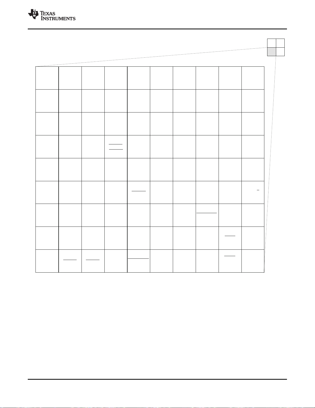
3.7.5 External Memory Interface A (EMIFA)
Table 3-7. External Memory Interface A (EMIFA) Terminal Functions
AM1806
SPRS658F –FEBRUARY 2010–REVISED MARCH 2014
SIGNAL
NAME NO.
TYPE
(1)
PULL
(2)
POWER
GROUP
EMA_D[15] / GP3[7] E6 I/O CP[17] B
EMA_D[14] / GP3[6] C7 I/O CP[17] B
EMA_D[13] / GP3[5] B6 I/O CP[17] B
EMA_D[12] / GP3[4] A6 I/O CP[17] B
EMA_D[11] / GP3[3] D6 I/O CP[17] B
EMA_D[10] / GP3[2] A7 I/O CP[17] B
EMA_D[9] / GP3[1] D9 I/O CP[17] B
EMA_D[8] / GP3[0] E10 I/O CP[17] B
EMA_D[7] / GP4[15] D7 I/O CP[17] B
EMA_D[6] / GP4[14] C6 I/O CP[17] B
EMA_D[5] / GP4[13] E7 I/O CP[17] B
EMA_D[4] / GP4[12] B5 I/O CP[17] B
EMA_D[3] / GP4[11] E8 I/O CP[17] B
EMA_D[2] / GP4[10] B8 I/O CP[17] B
EMA_D[1] / GP4[9] A8 I/O CP[17] B
EMA_D[0] / GP4[8] C9 I/O CP[17] B
(3)
EMIFA data bus
DESCRIPTION
(1) I = Input, O = Output, I/O = Bidirectional, Z = High impedance, PWR = Supply voltage, GND = Ground, A = Analog signal.
Note: The pin type shown refers to the input, output or high-impedance state of the pin function when configured as the signal name
highlighted in bold. All multiplexed signals may enter a high-impedance state when the configured function is input-only or the configured
function supports high-Z operation. All GPIO signals can be used as input or output. For multiplexed pins where functions have different
types (ie., input versus output), the table reflects the pin function direction for that particular peripheral.
(2) IPD = Internal Pulldown resistor; IPU = Internal Pullup resistor; CP[n] = configurable pull-up/pull-down (where n is the pin group) using
the PUPDENA and PUPDSEL registers in the System Module. The pull-up and pull-down control of these pins is not active until the
device is out of reset. During reset, all of the pins associated with these registers are pulled down. If the application requires a pull-up,
an external pull-up can be used. For more detailed information on pullup/pulldown resistors and situations where external
pullup/pulldown resistors are required, see the Device Configuration section. For electrical specifications on pullup and internal pulldown
circuits, see the Device Operating Conditions section.
(3) This signal is part of a dual-voltage IO group (A, B or C). These groups can be operated at 3.3V or 1.8V nominal. The three groups can
be operated at independent voltages but all pins withina group will operate at the same voltage. Group A operates at the voltage of
power supply DVDD3318_A. Group B operates at the voltage of power supply DVDD3318_B. Group C operates at the voltage of power
supply DVDD3318_C.
Copyright © 2010–2014, Texas Instruments Incorporated Device Overview 21
Submit Documentation Feedback
Product Folder Links: AM1806
AM1806
SPRS658F –FEBRUARY 2010–REVISED MARCH 2014
Table 3-7. External Memory Interface A (EMIFA) Terminal Functions (continued)
SIGNAL
NAME NO.
EMA_A[22] / MMCSD0_CMD /
PRU1_R30[30] / GP4[6]
EMA_A[21] / MMCSD0_DAT[0] /
PRU1_R30[29] / GP4[5]
EMA_A[20] / MMCSD0_DAT[1] /
PRU1_R30[28] / GP4[4]
EMA_A[19] / MMCSD0_DAT[2] /
PRU1_R30[27] / GP4[3]
EMA_A[18] / MMCSD0_DAT[3] /
PRU1_R30[26] / GP4[2]
EMA_A[17] / MMCSD0_DAT[4] /
PRU1_R30[25] / GP4[1]
EMA_A[16] / MMCSD0_DAT[5] /
PRU1_R30[24] / GP4[0]
EMA_A[15] / MMCSD0_DAT[6] /
PRU1_R30[23] / GP5[15] / PRU1_R31[23]
EMA_A[14] / MMCSD0_DAT[7] /
PRU1_R30[22] / GP5[14] / PRU1_R31[22]
EMA_A[13] /PRU0_R30[21] / PRU1_R30[21]
/ GP5[13] / PRU1_R31[21]
EMA_A[12] / PRU1_R30[20] / GP5[12] /
PRU1_R31[20]
EMA_A[11] / PRU1_R30[19] / GP5[11] /
PRU1_R31[19]
EMA_A[10] / PRU1_R30[18] / GP5[10] /
PRU1_R31[18]
A10 O CP[18] B
B10 O CP[18] B
A11 O CP[18] B
C10 O CP[18] B
E11 O CP[18] B
B11 O CP[18] B EMIFA address bus
E12 O CP[18] B
C11 O CP[19] B
A12 O CP[19] B
D11 O CP[19] B
D13 O CP[19] B
B12 O CP[19] B
C12 O CP[19] B
TYPE
(1)
PULL
EMA_A[9] / PRU1_R30[17] / GP5[9] D12 O CP[19] B
EMA_A[8] / PRU1_R30[16] / GP5[8] A13 O CP[19] B
EMA_A[7] / PRU1_R30[15] / GP5[7] B13 O CP[20] B
EMA_A[6] / GP5[6] E13 O CP[20] B
EMA_A[5] / GP5[5] C13 O CP[20] B
EMA_A[4] / GP5[4] A14 O CP[20] B
EMA_A[3] / GP5[3] D14 O CP[20] B
EMA_A[2] / GP5[2] B14 O CP[20] B
EMA_A[1] / GP5[1] D15 O CP[20] B
EMA_A[0] / GP5[0] C14 O CP[20] B
EMA_BA[0] / GP2[8] C15 O CP[16] B
EMA_BA[1] / GP2[9] A15 O CP[16] B
EMA_CLK / PRU0_R30[5] / GP2[7] /
PRU0_R31[5]
EMA_SDCKE / PRU0_R30[4] / GP2[6] /
PRU0_R31[4]
EMA_RAS / PRU0_R30[3] / GP2[5] /
PRU0_R31[3]
EMA_CAS / PRU0_R30[2] / GP2[4] /
PRU0_R31[2]
B7 O CP[16] B EMIFA clock
D8 O CP[16] B EMIFA SDRAM clock enable
A16 O CP[16] B EMIFA SDRAM row address strobe
A9 O CP[16] B EMIFA SDRAM column address strobe
EMA_CS[0] / GP2[0] A18 O CP[16] B EMIFA SDRAM Chip Select
EMA_CS[2] / GP3[15] B17 O CP[16] B
EMA_CS[3] / GP3[14] A17 O CP[16] B
EMA_CS[4] / GP3[13] F9 O CP[16] B
EMA_CS[5] / GP3[12] B16 O CP[16] B
EMA_A_RW / GP3[9] D10 O CP[16] B EMIFA Async Read/Write control
(2)
POWER
GROUP
(3)
EMIFA address bus
EMIFA bank address
EMIFA Async Chip Select
DESCRIPTION
www.ti.com
22 Device Overview Copyright © 2010–2014, Texas Instruments Incorporated
Submit Documentation Feedback
Product Folder Links: AM1806
AM1806
www.ti.com
SPRS658F –FEBRUARY 2010–REVISED MARCH 2014
Table 3-7. External Memory Interface A (EMIFA) Terminal Functions (continued)
SIGNAL
NAME NO.
TYPE
(1)
PULL
EMA_WE / GP3[11] B9 O CP[16] B EMIFA SDRAM write enable
EMA_WEN_DQM[1] / GP2[2] A5 O CP[16] B
EMA_WEN_DQM[0] / GP2[3] C8 O CP[16] B EMIFA write enable/data mask for EMA_D[7:0]
EMA_OE / GP3[10] B15 O CP[16] B EMIFA output enable
EMA_WAIT[0] / PRU0_R30[0] / GP3[8] /
PRU0_R31[0]
EMA_WAIT[1] / PRU0_R30[1] / GP2[1] /
PRU0_R31[1]
B18 I CP[16] B
B19 I CP[16] B
(2)
POWER
GROUP
(3)
DESCRIPTION
EMIFA write enable/data mask for
EMA_D[15:8]
EMIFA wait input/interrupt
Copyright © 2010–2014, Texas Instruments Incorporated Device Overview 23
Submit Documentation Feedback
Product Folder Links: AM1806
AM1806
SPRS658F –FEBRUARY 2010–REVISED MARCH 2014
3.7.6 DDR2/mDDR Memory Controller
Table 3-8. DDR2/mDDR Terminal Functions
www.ti.com
SIGNAL
NAME NO.
DDR_D[15] W10 I/O IPD
DDR_D[14] U11 I/O IPD
DDR_D[13] V10 I/O IPD
DDR_D[12] U10 I/O IPD
DDR_D[11] T12 I/O IPD
DDR_D[10] T10 I/O IPD
DDR_D[9] T11 I/O IPD
DDR_D[8] T13 I/O IPD
DDR_D[7] W11 I/O IPD
DDR_D[6] W12 I/O IPD
DDR_D[5] V12 I/O IPD
DDR_D[4] V13 I/O IPD
DDR_D[3] U13 I/O IPD
DDR_D[2] V14 I/O IPD
DDR_D[1] U14 I/O IPD
DDR_D[0] U15 I/O IPD
DDR_A[13] T5 O IPD
DDR_A[12] V4 O IPD
DDR_A[11] T4 O IPD
DDR_A[10] W4 O IPD
DDR_A[9] T6 O IPD
DDR_A[8] U4 O IPD
DDR_A[7] U6 O IPD
DDR_A[6] W5 O IPD
DDR_A[5] V5 O IPD
DDR_A[4] U5 O IPD
DDR_A[3] V6 O IPD
DDR_A[2] W6 O IPD
DDR_A[1] T7 O IPD
DDR_A[0] U7 O IPD
DDR_CLKP W8 O IPD DDR2 clock (positive)
DDR_CLKN W7 O IPD DDR2 clock (negative)
DDR_CKE V7 O IPD DDR2 clock enable
DDR_WE T8 O IPD DDR2 write enable
DDR_RAS W9 O IPD DDR2 row address strobe
DDR_CAS U9 O IPD DDR2 column address strobe
DDR_CS V9 O IPD DDR2 chip select
TYPE
(1)
PULL
(2)
DDR2 SDRAM data bus
DDR2 row/column address
DESCRIPTION
(1) I = Input, O = Output, I/O = Bidirectional, Z = High impedance, PWR = Supply voltage, GND = Ground, A = Analog signal.
Note: The pin type shown refers to the input, output or high-impedance state of the pin function when configured as the signal name
highlighted in bold. All multiplexed signals may enter a high-impedance state when the configured function is input-only or the configured
function supports high-Z operation. All GPIO signals can be used as input or output. For multiplexed pins where functions have different
types (ie., input versus output), the table reflects the pin function direction for that particular peripheral.
(2) IPD = Internal Pulldown resistor; IPU = Internal Pullup resistor; CP[n] = configurable pull-up/pull-down (where n is the pin group) using
the PUPDENA and PUPDSEL registers in the System Module. For more detailed information on pullup/pulldown resistors and situations
where external pullup/pulldown resistors are required, see the Device Configuration section. For electrical specifications on pullup and
internal pulldown circuits, see the Device Operating Conditions section.
24 Device Overview Copyright © 2010–2014, Texas Instruments Incorporated
Submit Documentation Feedback
Product Folder Links: AM1806
AM1806
www.ti.com
SPRS658F –FEBRUARY 2010–REVISED MARCH 2014
Table 3-8. DDR2/mDDR Terminal Functions (continued)
SIGNAL
NAME NO.
DDR_DQM[0] W13 O IPD
DDR_DQM[1] R10 O IPD
DDR_DQS[0] T14 I/O IPD
DDR_DQS[1] V11 I/O IPD
DDR_BA[2] U8 O IPD
DDR_BA[1] T9 O IPD DDR2 SDRAM bank address
DDR_BA[0] V8 O IPD
DDR_DQGATE0 R11 O IPD Route to DDR and back to DDR_DQGATE1 with
DDR_DQGATE1 R12 I IPD Route to DDR and back to DDR_DQGATE0 with
DDR_ZP U12 O — of N and P channel outputs. Tie to ground via 50
DDR_VREF R6 I — Note even in the case of mDDR an external resistor
N10, P10, N9,
DDR_DVDD18 PWR — DDR PHY 1.8V power supply pins
P9, R9, P8,
R8, P7, R7,
N6
TYPE
(1)
PULL
(2)
DESCRIPTION
DDR2 data mask outputs
DDR2 data strobe inputs/outputs
DDR2 loopback signal for external DQS gating.
same constraints as used for DDR clock and data.
DDR2 loopback signal for external DQS gating.
same constraints as used for DDR clock and data.
DDR2 reference output for drive strength calibration
ohm resistor @ 5% tolerance.
DDR voltage input for the DDR2/mDDR I/O buffers.
divider connected to this pin is necessary.
Copyright © 2010–2014, Texas Instruments Incorporated Device Overview 25
Submit Documentation Feedback
Product Folder Links: AM1806
AM1806
SPRS658F –FEBRUARY 2010–REVISED MARCH 2014
3.7.7 Serial Peripheral Interface Modules (SPI)
Table 3-9. Serial Peripheral Interface (SPI) Terminal Functions
www.ti.com
SIGNAL
NAME NO.
TYPE
(1)
PULL
(2)
POWER
GROUP
(3)
DESCRIPTION
SPI0
SPI0_CLK / EPWM0A / GP1[8] D19 I/O CP[7] A SPI0 clock
SPI0_ENA / EPWM0B / PRU0_R30[6] C17 I/O CP[7] A SPI0 enable
SPI0_SCS[0] / TM64P1_OUT12 / GP1[6] / TM64P1_IN12 D17 I/O CP[10] A
SPI0_SCS[1] / TM64P0_OUT12 / GP1[7] / TM64P0_IN12 E16 I/O CP[10] A
SPI0_SCS[2] / UART0_RTS / GP8[1] D16 I/O CP[9] A
SPI0_SCS[3] / UART0_CTS / GP8[2] E17 I/O CP[9] A
SPI0 chip selects
SPI0_SCS[4] / UART0_TXD / GP8[3] D18 I/O CP[8] A
SPI0_SCS[5] / UART0_RXD / GP8[4] C19 I/O CP[8] A
SPI0_SIMO / EPWMSYNCO / GP8[5] C18 I/O CP[7] A
SPI0_SOMI / EPWMSYNCI / GP8[6] C16 I/O CP[7] A
SPI0 data slave-inmaster-out
SPI0 data slave-outmaster-in
SPI1
SPI1_CLK / GP2[13] G19 I/O CP[15] A SPI1 clock
SPI1_ENA / GP2[12] H16 I/O CP[15] A SPI1 enable
SPI1_SCS[0] / EPWM1B / PRU0_R30[7] / GP2[14] / TM64P3_IN12 E19 I/O CP[14] A
SPI1_SCS[1] / EPWM1A / PRU0_R30[8] / GP2[15] / TM64P2_IN12 F18 I/O CP[14] A
SPI1_SCS[2] / UART1_TXD / GP1[0] F19 I/O CP[13] A
SPI1_SCS[3] / UART1_RXD / GP1[1] E18 I/O CP[13] A
SPI1_SCS[4] / UART2_TXD / I2C1_SDA /GP1[2] F16 I/O CP[12] A
SPI1 chip selects
SPI1_SCS[5] / UART2_RXD / I2C1_SCL /GP1[3] F17 I/O CP[12] A
SPI1_SCS[6] / I2C0_SDA / TM64P3_OUT12 / GP1[4] G18 I/O CP[11] A
SPI1_SCS[7] / I2C0_SCL / TM64P2_OUT12 / GP1[5] G16 I/O CP[11] A
SPI1_SIMO / GP2[10] G17 I/O CP[15] A
SPI1_SOMI / GP2[11] H17 I/O CP[15] A
SPI1 data slave-inmaster-out
SPI1 data slave-outmaster-in
(1) I = Input, O = Output, I/O = Bidirectional, Z = High impedance, PWR = Supply voltage, GND = Ground, A = Analog signal.
Note: The pin type shown refers to the input, output or high-impedance state of the pin function when configured as the signal name
highlighted in bold. All multiplexed signals may enter a high-impedance state when the configured function is input-only or the configured
function supports high-Z operation. All GPIO signals can be used as input or output. For multiplexed pins where functions have different
types (ie., input versus output), the table reflects the pin function direction for that particular peripheral.
(2) IPD = Internal Pulldown resistor; IPU = Internal Pullup resistor; CP[n] = configurable pull-up/pull-down (where n is the pin group) using
the PUPDENA and PUPDSEL registers in the System Module. The pull-up and pull-down control of these pins is not active until the
device is out of reset. During reset, all of the pins associated with these registers are pulled down. If the application requires a pull-up,
an external pull-up can be used. For more detailed information on pullup/pulldown resistors and situations where external
pullup/pulldown resistors are required, see the Device Configuration section. For electrical specifications on pullup and internal pulldown
circuits, see the Device Operating Conditions section.
(3) This signal is part of a dual-voltage IO group (A, B or C). These groups can be operated at 3.3V or 1.8V nominal. The three groups can
be operated at independent voltages but all pins withina group will operate at the same voltage. Group A operates at the voltage of
power supply DVDD3318_A. Group B operates at the voltage of power supply DVDD3318_B. Group C operates at the voltage of power
supply DVDD3318_C.
26 Device Overview Copyright © 2010–2014, Texas Instruments Incorporated
Submit Documentation Feedback
Product Folder Links: AM1806
www.ti.com
3.7.8 Programmable Real-Time Unit (PRU)
Table 3-10. Programmable Real-Time Unit (PRU) Terminal Functions
AM1806
SPRS658F –FEBRUARY 2010–REVISED MARCH 2014
SIGNAL
NAME NO.
TYPE
(1)
PULL
(2)
POWER
GROUP
PRU0 Signals
PRU0_R30[31] / UHPI_HRDY / PRU1_R30[12] / GP6[13] R17 O CP[23] C
PRU0_R30[30] / UHPI_HINT / PRU1_R30[11] / GP6[12] R16 O CP[23] C
PRU0_R30[29] / UHPI_HCNTL0 / UPP_CHA_CLOCK / GP6[11] U17 O CP[24] C
PRU0_R30[28] / UHPI_HCNTL1 / UPP_CHA_START / GP6[10] W15 O CP[24] C
PRU0_R30[27] / UHPI_HHWIL / UPP_CHA_ENABLE / GP6[9] U16 O CP[24] C
PRU0_R30[26] / UHPI_HRW / / UPP_CHA_WAITGP6[8] / PRU1_R31[17] T15 O CP[24] C
PRU0_R30[25] / MMCSD1_DAT[0] / UPP_CHB_CLOCK / GP8[15] /
PRU1_R31[27]
PRU0_R30[24] / MMCSD1_CLK / UPP_CHB_START / GP8[14] /
PRU1_R31[26]
PRU0_R30[23] / MMCSD1_CMD / UPP_CHB_ENABLE / GP8[13] /
PRU1_R31[25]
PRU0_R30[22] / PRU1_R30[8] / UPP_CHB_WAIT / GP8[12] /
PRU1_R31[24]
G1 O CP30] C
G2 O CP[30] C
J4 O CP[30] C
G3 O CP[30] C
EMA_A[13] / PRU0_R30[21] / PRU1_R30[21] / GP5[13] / PRU1_R31[21] D11 O CP[19] B
ACLKR / PRU0_R30[20] / GP0[15] / PRU0_R31[22] A1 O CP[0] A
ACLKX / PRU0_R30[19] / GP0[14] / PRU0_R31[21] B1 O CP[0] A
AHCLKR / PRU0_R30[18] / UART1_RTS / GP0[11] / PRU0_R31[18] A2 O CP[0] A
AXR7 / EPWM1TZ[0] / PRU0_R30[17] / GP1[15] / PRU0_R31[7] D2 O CP[4] A
AMUTE / PRU0_R30[16] / UART2_RTS / GP0[9] / PRU0_R31[16] D5 O CP[0] A
VP_DIN[15]_VSYNC / UHPI_HD[7] / UPP_D[7] / PRU0_R30[15] /
PRU0_R31[15]
VP_DIN[14]_HSYNC / UHPI_HD[6] / UPP_D[6] / PRU0_R30[14] /
PRU0_R31[14]
VP_DIN[13]_FIELD / UHPI_HD[5] / UPP_D[5] / PRU0_R30[13] /
PRU0_R31[13]
V18 O CP[27] C
V19 O CP[27] C
U19 O CP[27] C
VP_DIN[12] / UHPI_HD[4] / UPP_D[4] / PRU0_R30[12] / PRU0_R31[12] T16 O CP[27] C
VP_DIN[11] / UHPI_HD[3] / UPP_D[3] / PRU0_R30[11] / PRU0_R31[11] R18 O CP[27] C
VP_DIN[10] / UHPI_HD[2] / UPP_D[2] / PRU0_R30[10] / PRU0_R31[10] R19 O CP[27] C
VP_DIN[9] / UHPI_HD[1] / UPP_D[1] / PRU0_R30[9] / PRU0_R31[9] R15 O CP[27] C
SPI1_SCS[1] / EPWM1A / PRU0_R30[8] / GP2[15] / TM64P2_IN12 F18 O CP[14] A
SPI1_SCS[0] / EPWM1B / PRU0_R30[7] / GP2[14] / TM64P3_IN12 E19 O CP[14] A
SPI0_ENA / EPWM0B / PRU0_R30[6] C17 O CP[7] A
DESCRIPTION
(3)
PRU0 Output
Signals
(1) I = Input, O = Output, I/O = Bidirectional, Z = High impedance, PWR = Supply voltage, GND = Ground, A = Analog signal.
Note: The pin type shown refers to the input, output or high-impedance state of the pin function when configured as the signal name
highlighted in bold. All multiplexed signals may enter a high-impedance state when the configured function is input-only or the configured
function supports high-Z operation. All GPIO signals can be used as input or output. For multiplexed pins where functions have different
types (ie., input versus output), the table reflects the pin function direction for that particular peripheral.
(2) IPD = Internal Pulldown resistor; IPU = Internal Pullup resistor; CP[n] = configurable pull-up/pull-down (where n is the pin group) using
the PUPDENA and PUPDSEL registers in the System Module. The pull-up and pull-down control of these pins is not active until the
device is out of reset. During reset, all of the pins associated with these registers are pulled down. If the application requires a pull-up,
an external pull-up can be used. For more detailed information on pullup/pulldown resistors and situations where external
pullup/pulldown resistors are required, see the Device Configuration section. For electrical specifications on pullup and internal pulldown
circuits, see the Device Operating Conditions section.
(3) This signal is part of a dual-voltage IO group (A, B or C). These groups can be operated at 3.3V or 1.8V nominal. The three groups can
be operated at independent voltages but all pins withina group will operate at the same voltage. Group A operates at the voltage of
power supply DVDD3318_A. Group B operates at the voltage of power supply DVDD3318_B. Group C operates at the voltage of power
supply DVDD3318_C.
Copyright © 2010–2014, Texas Instruments Incorporated Device Overview 27
Submit Documentation Feedback
Product Folder Links: AM1806
AM1806
SPRS658F –FEBRUARY 2010–REVISED MARCH 2014
Table 3-10. Programmable Real-Time Unit (PRU) Terminal Functions (continued)
SIGNAL
NAME NO.
TYPE
(1)
PULL
EMA_CLK / PRU0_R30[5] / GP2[7] / PRU0_R31[5] B7 O CP[16] B
EMA_SDCKE / PRU0_R30[4] / GP2[6] / PRU0_R31[4] D8 O CP[16] B
EMA_RAS / PRU0_R30[3] / GP2[5] / PRU0_R31[3] A16 O CP[16] B
EMA_CAS / PRU0_R30[2] / GP2[4] / PRU0_R31[2] A9 O CP[16] B
EMA_WAIT[1] / PRU0_R30[1] / GP2[1] / PRU0_R31[1] B19 O CP[16] B
EMA_WAIT[0] / PRU0_R30[0] / GP3[8] / PRU0_R31[0] B18 O CP[16] B
VP_DIN[7] / UHPI_HD[15] / UPP_D[15] / PRU0_R31[29] U18 I CP[26] C
VP_DIN[6] / UHPI_HD[14] / UPP_D[14] / PRU0_R31[28] V16 I CP[26] C
VP_DIN[5] / UHPI_HD[13] / UPP_D[13] / PRU0_R31[27] R14 I CP[26] C
VP_DIN[4] / UHPI_HD[12] / UPP_D[12] / PRU0_R31[26] W16 I CP[26] C
VP_DIN[3] / UHPI_HD[11] / UPP_D[11] / PRU0_R31[25] V17 I CP[26] C
VP_DIN[2] / UHPI_HD[10] / UPP_D[10] / PRU0_R31[24] W17 I CP[26] C
VP_DIN[1] / UHPI_HD[9]UPP_D[9] / PRU0_R31[23] W18 I CP[26] C
ACLKR / PRU0_R30[20] / GP0[15] / PRU0_R31[22] A1 I CP[0] A
ACLKX / PRU0_R30[19] / GP0[14] / PRU0_R31[21] B1 I CP[0] A
AFSR / GP0[13] / PRU0_R31[20] C2 I CP[0] A
AFSX / GP0[12] / PRU0_R31[19] B2 I CP[0] A
AHCLKR / PRU0_R30[18] / UART1_RTS / GP0[11] / PRU0_R31[18] A2 I CP[0] A
AHCLKX / USB_REFCLKIN / UART1_CTS / GP0[10] / PRU0_R31[17] A3 I CP[0] A
AMUTE / PRU0_R30[16] / UART2_RTS / GP0[9] / PRU0_R31[16] D5 I CP[0] A
VP_DIN[15]_VSYNC / UHPI_HD[7] / UPP_D[7] / PRU0_R30[15] /
PRU0_R31[15]
VP_DIN[14]_HSYNC / UHPI_HD[6] / UPP_D[6] / PRU0_R30[14] /
PRU0_R31[14]
VP_DIN[13]_FIELD / UHPI_HD[5] / UPP_D[5] / PRU0_R30[13] /
PRU0_R31[13]
V18 I CP[27] C
V19 I CP[27] C
U19 I CP[27] C
VP_DIN[12] / UHPI_HD[4] / UPP_D[4] / PRU0_R30[12] / PRU0_R31[12] T16 I CP[27] C
VP_DIN[11] / UHPI_HD[3] / UPP_D[3] / PRU0_R30[11] / PRU0_R31[11] R18 I CP[27] C
VP_DIN[10] / UHPI_HD[2] / UPP_D[2] / PRU0_R30[10] / PRU0_R31[10] R19 I CP[27] C
VP_DIN[9] / UHPI_HD[1] / UPP_D[1] / PRU0_R30[9] / PRU0_R31[9] R15 I CP[27] C
AXR8 / CLKS1 / ECAP1_APWM1 / GP0[0] / PRU0_R31[8] E4 I CP[3] A
AXR7 / EPWM1TZ[0] / PRU0_R30[17] / GP1[15] / PRU0_R31[7] D2 I CP[4] A
AXR6 / CLKR0 / GP1[14] / PRU0_R31[6] C1 I CP[5] A
EMA_CLK / PRU0_R30[5] / GP2[7] / PRU0_R31[5] B7 I CP[16] B
EMA_SDCKE / PRU0_R30[4] / GP2[6] / PRU0_R31[4] D8 I CP[16] B
EMA_RAS / PRU0_R30[3] / GP2[5] / PRU0_R31[3] A16 I CP[16] B
EMA_CAS / PRU0_R30[2] / GP2[4] / PRU0_R31[2] A9 I CP[16] B
EMA_WAIT[1] / PRU0_R30[1] / GP2[1] / PRU0_R31[1] B19 I CP[16] B
EMA_WAIT[0] / PRU0_R30[0] / GP3[8] / PRU0_R31[0] B18 I CP[16] B
(2)
POWER
GROUP
DESCRIPTION
(3)
PRU0 Output
Signals
PRU0 Input
Signals
www.ti.com
28 Device Overview Copyright © 2010–2014, Texas Instruments Incorporated
Submit Documentation Feedback
Product Folder Links: AM1806
www.ti.com
SPRS658F –FEBRUARY 2010–REVISED MARCH 2014
Table 3-10. Programmable Real-Time Unit (PRU) Terminal Functions (continued)
SIGNAL
NAME NO.
TYPE
(1)
PULL
PRU1 Signals
MMCSD0_CLK / PRU1_R30[31] /GP4[7] E9 O CP[18] B
EMA_A[22] / MMCSD0_CMD / PRU1_R30[30] / GP4[6] A10 O CP[18] B
EMA_A[21] / MMCSD0_DAT[0] / PRU1_R30[29] / GP4[5] B10 O CP[18] B
EMA_A[20] / MMCSD0_DAT[1] / PRU1_R30[28] / GP4[4] A11 O CP[18] B
EMA_A[19] / MMCSD0_DAT[2] / PRU1_R30[27] / GP4[3] C10 O CP[18] B
EMA_A[18] / MMCSD0_DAT[3] / PRU1_R30[26] / GP4[2] E11 O CP[18] B
EMA_A[17] / MMCSD0_DAT[4] / PRU1_R30[25] / GP4[1] B11 O CP[18] B
EMA_A[16] / MMCSD0_DAT[5] / PRU1_R30[24] / GP4[0] E12 O CP[18] B
EMA_A[15] / MMCSD0_DAT[6] / PRU1_R30[23] / GP5[15] /
PRU1_R31[23]
EMA_A[14] / MMCSD0_DAT[7] / PRU1_R30[22] / GP5[14] /
PRU1_R31[22]
C11 O CP[19] B
A12 O CP[19] B
EMA_A[13] / PRU0_R30[21] / PRU1_R30[21] / GP5[13] / PRU1_R31[21] D11 O CP[19] B
EMA_A[12] / PRU1_R30[20] / GP5[12] / PRU1_R31[20] D13 O CP[19] B
EMA_A[11] / PRU1_R30[19] / GP5[11] / PRU1_R31[19] B12 O CP[19] B
EMA_A[10] / PRU1_R30[18] / GP5[10] / PRU1_R31[18] C12 O CP[19] B
EMA_A[9] / PRU1_R30[17] / GP5[9] D12 O CP[19] B
EMA_A[8] / PRU1_R30[16] / GP5[8] A13 O CP[19] B
EMA_A[7] / PRU1_R30[15] / GP5[7] B13 O CP[20] B
RESETOUT / UHPI_HAS / PRU1_R30[14] / GP6[15] T17 O CP[21] C
CLKOUT / UHPI_HDS2 / PRU1_R30[13] / GP6[14] T18 O CP[22] C
PRU0_R30[31] / UHPI_HRDY / PRU1_R30[12] / GP6[13] R17 O CP[23] C
PRU0_R30[30] / UHPI_HINT / PRU1_R30[11] / GP6[12] R16 O CP[23] C
VP_CLKIN0 / UHPI_HCS / PRU1_R30[10] / GP6[7] / UPP_2xTXCLK W14 O CP[25] C
VP_CLKIN1 / UHPI_HDS1 / PRU1_R30[9] / GP6[6] / PRU1_R31[16] V15 O CP[25] C
PRU0_R30[22] / PRU1_R30[8] / UPP_CHB_WAIT / GP8[12] /
PRU1_R31[24]
G3 O CP[30] C
MMCSD1_DAT[7] / LCD_PCLK / PRU1_R30[7] / GP8[11] F1 O CP[31] C
MMCSD1_DAT[6] / LCD_MCLK / PRU1_R30[6] / GP8[10] / PRU1_R31[7] F2 O CP[31] C
MMCSD1_DAT[5] / LCD_HSYNC / PRU1_R30[5] / GP8[9] / PRU1_R31[6] H4 O CP[31] C
MMCSD1_DAT[4] / LCD_VSYNC / PRU1_R30[4] / GP8[8] / PRU1_R31[5] G4 O CP[31] C
VP_CLKIN2 / MMCSD1_DAT[3] / PRU1_R30[3] / GP6[4] / PRU1_R31[4] H3 O CP[30] C
VP_CLKOUT2 / MMCSD1_DAT[2] / PRU1_R30[2] / GP6[3] /
PRU1_R31[3]
K3 O CP[30] C
VP_CLKIN3 / MMCSD1_DAT[1] / PRU1_R30[1] / GP6[2] / PRU1_R31[2] J3 O CP[30] C
VP_CLKOUT3 / PRU1_R30[0] / GP6[1] / PRU1_R31[1] K4 O CP[30] C
(2)
POWER
GROUP
DESCRIPTION
(3)
PRU1 Output
Signals
AM1806
Copyright © 2010–2014, Texas Instruments Incorporated Device Overview 29
Submit Documentation Feedback
Product Folder Links: AM1806
AM1806
SPRS658F –FEBRUARY 2010–REVISED MARCH 2014
Table 3-10. Programmable Real-Time Unit (PRU) Terminal Functions (continued)
SIGNAL
NAME NO.
TYPE
(1)
PULL
VP_DIN[0] / UHPI_HD[8] / UPP_D[8] / PRU1_R31[29] W19 I CP[26] C
LCD_AC_ENB_CS / GP6[0] / PRU1_R31[28] R5 I CP[31] C
PRU0_R30[25] / MMCSD1_DAT[0] / UPP_CHB_CLOCK / GP8[15] /
PRU1_R31[27]
PRU0_R30[24] / MMCSD1_CLK / UPP_CHB_START / GP8[14] /
PRU1_R31[26]
PRU0_R30[23] / MMCSD1_CMD / UPP_CHB_ENABLE / GP8[13] /
PRU1_R31[25]
PRU0_R30[22] / PRU1_R30[8] / UPP_CHB_WAIT / GP8[12] /
PRU1_R31[24]
G1 I CP[30] C
G2 I CP[30] C
J4 I CP[30] C
G3 I CP[30] C
EMA_A[15] / MMCSD0_DAT[6] / PRU1_R30[23] / GP[15] / PRU1_R31[23] C11 I CP[19] B
EMA_A[14] / MMCSD0_DAT[7] / PRU1_R30[22] /GP[14] / PRU1_R31[22] A12 I CP[19] B
EMA_A[13] / PRU0_R30[21] / PRU1_R30[21] /GP[13] / PRU1_R31[21] D11 I CP[19] B
EMA_A[12] / PRU1_R30[20] / GP[12] / PRU1_R31[20] D13 I CP[19] B
EMA_A[11] / PRU1_R30[19] /GP[11] / PRU1_R31[19] B12 I CP[19] B
EMA_A[10] / PRU1_R30[18] /GP[10] / PRU1_R31[18] C12 I CP[19] B
PRU0_R30[26] / UHPI_HRW / UPP_CHA_WAIT / GP6[8] / PRU1_R31[17] T15 I CP[24] C
VP_CLKIN1 / UHPI_HDS1 / PRU1_R30[9] / GP6[6] / PRU1_R31[16] V15 I CP[25] C
VP_DOUT[7] / LCD_D[7] / UPP_XD[15] / GP7[15] / PRU1_R31[15] U2 I CP[28] C
VP_DOUT[6] / LCD_D[6] / UPP_XD[14] / GP7[14] / PRU1_R31[14] U1 I CP[28] C
VP_DOUT[5] / LCD_D[5] / UPP_XD[13] / GP7[13] / PRU1_R31[13] V3 I CP[28] C
VP_DOUT[4] / LCD_D[4] / UPP_XD[12] / GP7[12] / PRU1_R31[12] V2 I CP[28] C
VP_DOUT[3] / LCD_D[3] / UPP_XD[11] / GP7[11] / PRU1_R31[11] V1 I CP[28] C
VP_DOUT[2] / LCD_D[2] / UPP_XD[10] / GP7[10] / PRU1_R31[10] W3 I CP[28] C
VP_DOUT[1] / LCD_D[1] / UPP_XD[9] / GP7[9] / PRU1_R31[9] W2 I CP[28] C
VP_DOUT[0] / LCD_D[0] / UPP_XD[8] / GP7[8] / PRU1_R31[8] W1 I CP[28] C
MMCSD1_DAT[6] / LCD_MCLK / PRU1_R30[6] / GP8[10] / PRU1_R31[7] F2 I CP[31] C
MMCSD1_DAT[5] / LCD_HSYNC / PRU1_R30[5] / GP8[9] / PRU1_R31[6] H4 I CP[31] C
MMCSD1_DAT[4] / LCD_VSYNC / PRU1_R30[4] / GP8[8] / PRU1_R31[5] G4 I CP[31] C
VP_CLKIN2 / MMCSD1_DAT[3] / PRU1_R30[3] / GP6[4] / PRU1_R31[4] H3 I CP[30] C
VP_CLKOUT2 / MMCSD1_DAT[2] / PRU1_R30[2] / GP6[3] /
PRU1_R31[3]
K3 I CP[30] C
VP_CLKIN3 / MMCSD1_DAT[1] / PRU1_R30[1] / GP6[2] / PRU1_R31[2] J3 I CP[30] C
VP_CLKOUT3 / PRU1_R30[0] / GP6[1] / PRU1_R31[1] K4 I CP[30] C
VP_DIN[8] / UHPI_HD[0] / UPP_D[0] / GP6[5] / PRU1_R31[0] P17 I CP[27] C
(2)
POWER
GROUP
DESCRIPTION
(3)
PRU1 Input
Signals
www.ti.com
30 Device Overview Copyright © 2010–2014, Texas Instruments Incorporated
Submit Documentation Feedback
Product Folder Links: AM1806

www.ti.com
3.7.9 Enhanced Capture/Auxiliary PWM Modules (eCAP0)
The eCAP Module pins function as either input captures or auxiliary PWM 32-bit outputs, depending upon
how the eCAP module is programmed.
Table 3-11. Enhanced Capture Module (eCAP) Terminal Functions
AM1806
SPRS658F –FEBRUARY 2010–REVISED MARCH 2014
SIGNAL
NAME NO.
AXR0 / ECAP0_APWM0 / GP8[7] / CLKS0 F3 I/O CP[6] A
AXR8 / CLKS1 / ECAP1_APWM1 / GP0[0] / PRU0_R31[8] E4 I/O CP[3] A
AXR15 / EPWM0TZ[0] / ECAP2_APWM2 / GP0[7] A4 I/O CP[1] A
(1) I = Input, O = Output, I/O = Bidirectional, Z = High impedance, PWR = Supply voltage, GND = Ground, A = Analog signal.
Note: The pin type shown refers to the input, output or high-impedance state of the pin function when configured as the signal name
highlighted in bold. All multiplexed signals may enter a high-impedance state when the configured function is input-only or the configured
function supports high-Z operation. All GPIO signals can be used as input or output. For multiplexed pins where functions have different
types (ie., input versus output), the table reflects the pin function direction for that particular peripheral.
(2) IPD = Internal Pulldown resistor; IPU = Internal Pullup resistor; CP[n] = configurable pull-up/pull-down (where n is the pin group) using
the PUPDENA and PUPDSEL registers in the System Module. The pull-up and pull-down control of these pins is not active until the
device is out of reset. During reset, all of the pins associated with these registers are pulled down. If the application requires a pull-up,
an external pull-up can be used. For more detailed information on pullup/pulldown resistors and situations where external
pullup/pulldown resistors are required, see the Device Configuration section. For electrical specifications on pullup and internal pulldown
circuits, see the Device Operating Conditions section.
(3) This signal is part of a dual-voltage IO group (A, B or C). These groups can be operated at 3.3V or 1.8V nominal. The three groups can
be operated at independent voltages but all pins withina group will operate at the same voltage. Group A operates at the voltage of
power supply DVDD3318_A. Group B operates at the voltage of power supply DVDD3318_B. Group C operates at the voltage of power
supply DVDD3318_C.
TYPE
eCAP0
eCAP1
eCAP2
(1)
PULL
(2)
POWER
GROUP
(3)
enhanced capture 0 input or
auxiliary PWM 0 output
enhanced capture 1 input or
auxiliary PWM 1 output
enhanced capture 2 input or
auxiliary PWM 2 output
DESCRIPTION
Copyright © 2010–2014, Texas Instruments Incorporated Device Overview 31
Submit Documentation Feedback
Product Folder Links: AM1806

AM1806
SPRS658F –FEBRUARY 2010–REVISED MARCH 2014
3.7.10 Enhanced Pulse Width Modulators (eHRPWM)
Table 3-12. Enhanced Pulse Width Modulator (eHRPWM) Terminal Functions
www.ti.com
SIGNAL
NAME NO.
TYPE
(1)
PULL
(2)
POWER
GROUP
(3)
DESCRIPTION
eHRPWM0
SPI0_CLK / EPWM0A / GP1[8] D19 I/O CP[7] A
eHRPWM0 A output
(with high-resolution)
SPI0_ENA / EPWM0B / PRU0_R30[6] C17 I/O CP[7] A eHRPWM0 B output
AXR15 / EPWM0TZ[0] / ECAP2_APWM2 / GP0[7] A4 I CP[1] A eHRPWM0 trip zone input
SPI0_SOMI / EPWMSYNCI / GP8[6] C16 I CP[7] A eHRPWM0 sync input
SPI0_SIMO / EPWMSYNCO / GP8[5] C18 I/O CP[7] A eHRPWM0 sync output
eHRPWM1
SPI1_SCS[1] / EPWM1A / PRU0_R30[8] / GP2[15] / eHRPWM1 A output
TM64P2_IN12 (with high-resolution)
SPI1_SCS[0] / EPWM1B / PRU0_R30[7] / GP2[14] /
TM64P3_IN12
AXR7 / EPWM1TZ[0] / PRU0_R30[17] / GP1[15] /
PRU0_R31[7]
F18 I/O CP[14] A
E19 I/O CP[14] A eHRPWM1 B output
D2 I CP[4] A eHRPWM1 trip zone input
(1) I = Input, O = Output, I/O = Bidirectional, Z = High impedance, PWR = Supply voltage, GND = Ground, A = Analog signal.
Note: The pin type shown refers to the input, output or high-impedance state of the pin function when configured as the signal name
highlighted in bold. All multiplexed signals may enter a high-impedance state when the configured function is input-only or the configured
function supports high-Z operation. All GPIO signals can be used as input or output. For multiplexed pins where functions have different
types (ie., input versus output), the table reflects the pin function direction for that particular peripheral.
(2) IPD = Internal Pulldown resistor; IPU = Internal Pullup resistor; CP[n] = configurable pull-up/pull-down (where n is the pin group) using
the PUPDENA and PUPDSEL registers in the System Module. The pull-up and pull-down control of these pins is not active until the
device is out of reset. During reset, all of the pins associated with these registers are pulled down. If the application requires a pull-up,
an external pull-up can be used. For more detailed information on pullup/pulldown resistors and situations where external
pullup/pulldown resistors are required, see the Device Configuration section. For electrical specifications on pullup and internal pulldown
circuits, see the Device Operating Conditions section.
(3) This signal is part of a dual-voltage IO group (A, B or C). These groups can be operated at 3.3V or 1.8V nominal. The three groups can
be operated at independent voltages but all pins withina group will operate at the same voltage. Group A operates at the voltage of
power supply DVDD3318_A. Group B operates at the voltage of power supply DVDD3318_B. Group C operates at the voltage of power
supply DVDD3318_C.
32 Device Overview Copyright © 2010–2014, Texas Instruments Incorporated
Submit Documentation Feedback
Product Folder Links: AM1806

www.ti.com
3.7.11 Boot
AM1806
SPRS658F –FEBRUARY 2010–REVISED MARCH 2014
Table 3-13. Boot Mode Selection Terminal Functions
SIGNAL
NAME NO.
TYPE
(2)
PULL
(3)
(1)
POWER
GROUP
(4)
DESCRIPTION
VP_DOUT[15] / LCD_D[15] / UPP_XD[7] /GP7[7] / BOOT[7] P4 I CP[29] C
VP_DOUT[14] / LCD_D[14] / UPP_XD[6] /GP7[6] / BOOT[6] R3 I CP[29] C
VP_DOUT[13] / LCD_D[13] / UPP_XD[5] /GP7[5] / BOOT[5] R2 I CP[29] C
VP_DOUT[12] / LCD_D[12] / UPP_XD[4] / GP7[4] / BOOT[4] R1 I CP[29] C
VP_DOUT[11] / LCD_D[11] / UPP_XD[3] /GP7[3] / BOOT[3] T3 I CP[29] C
Boot Mode Selection Pins
VP_DOUT[10] / LCD_D[10] / UPP_XD[2] /GP7[2] / BOOT[2] T2 I CP[29] C
VP_DOUT[9] / LCD_D[9] / UPP_XD[1] /GP7[1] / BOOT[1] T1 I CP[29] C
VP_DOUT[8] / LCD_D[8] / UPP_XD[0] /GP7[0] / BOOT[0] U3 I CP[29] C
(1) Boot decoding is defined in the bootloader application report.
(2) I = Input, O = Output, I/O = Bidirectional, Z = High impedance, PWR = Supply voltage, GND = Ground, A = Analog signal.
Note: The pin type shown refers to the input, output or high-impedance state of the pin function when configured as the signal name
highlighted in bold. All multiplexed signals may enter a high-impedance state when the configured function is input-only or the configured
function supports high-Z operation. All GPIO signals can be used as input or output. For multiplexed pins where functions have different
types (ie., input versus output), the table reflects the pin function direction for that particular peripheral.
(3) IPD = Internal Pulldown resistor; IPU = Internal Pullup resistor; CP[n] = configurable pull-up/pull-down (where n is the pin group) using
the PUPDENA and PUPDSEL registers in the System Module. The pull-up and pull-down control of these pins is not active until the
device is out of reset. During reset, all of the pins associated with these registers are pulled down. If the application requires a pull-up,
an external pull-up can be used. For more detailed information on pullup/pulldown resistors and situations where external
pullup/pulldown resistors are required, see the Device Configuration section. For electrical specifications on pullup and internal pulldown
circuits, see the Device Operating Conditions section.
(4) This signal is part of a dual-voltage IO group (A, B or C). These groups can be operated at 3.3V or 1.8V nominal. The three groups can
be operated at independent voltages but all pins withina group will operate at the same voltage. Group A operates at the voltage of
power supply DVDD3318_A. Group B operates at the voltage of power supply DVDD3318_B. Group C operates at the voltage of power
supply DVDD3318_C.
Copyright © 2010–2014, Texas Instruments Incorporated Device Overview 33
Submit Documentation Feedback
Product Folder Links: AM1806

AM1806
SPRS658F –FEBRUARY 2010–REVISED MARCH 2014
3.7.12 Universal Asynchronous Receiver/Transmitters (UART0, UART1, UART2)
Table 3-14. Universal Asynchronous Receiver/Transmitter (UART) Terminal Functions
www.ti.com
SIGNAL
NAME NO.
TYPE
(1)
PULL
POWER
(2)
GROUP
(3)
DESCRIPTION
UART0
SPI0_SCS[5] / UART0_RXD / GP8[4] C19 I CP[8] A UART0 receive data
SPI0_SCS[4] / UART0_TXD / GP8[3] D18 O CP[8] A UART0 transmit data
SPI0_SCS[2] / UART0_RTS / GP8[1] D16 O CP[9] A UART0 ready-to-send output
SPI0_SCS[3] / UART0_CTS / GP8[2] E17 I CP[9] A UART0 clear-to-send input
UART1
SPI1_SCS[3] / UART1_RXD / GP1[1] E18 I CP[13] A UART1 receive data
SPI1_SCS[2] / UART1_TXD / GP1[0] F19 O CP[13] A UART1 transmit data
AHCLKR / PRU0_R30[18] / UART1_RTS / GP0[11] /
PRU0_R31[18]
AHCLKX / USB_REFCLKIN / UART1_CTS / GP0[10] /
PRU0_R31[17]
A2 O CP[0] A UART1 ready-to-send output
A3 I CP[0] A UART1 clear-to-send input
UART2
SPI1_SCS[5] / UART2_RXD / I2C1_SCL / GP1[3] F17 I CP[12] A UART2 receive data
SPI1_SCS[4] / UART2_TXD / I2C1_SDA / GP1[2] F16 O CP[12] A UART2 transmit data
AMUTE / PRU0_R30[16] / UART2_RTS / GP0[9] /
PRU0_R31[16]
D5 O CP[0] A UART2 ready-to-send output
RTC_ALARM / UART2_CTS / GP0[8] / DEEPSLEEP F4 I CP[0] A UART2 clear-to-send input
(1) I = Input, O = Output, I/O = Bidirectional, Z = High impedance, PWR = Supply voltage, GND = Ground, A = Analog signal.
Note: The pin type shown refers to the input, output or high-impedance state of the pin function when configured as the signal name
highlighted in bold. All multiplexed signals may enter a high-impedance state when the configured function is input-only or the configured
function supports high-Z operation. All GPIO signals can be used as input or output. For multiplexed pins where functions have different
types (ie., input versus output), the table reflects the pin function direction for that particular peripheral.
(2) IPD = Internal Pulldown resistor; IPU = Internal Pullup resistor; CP[n] = configurable pull-up/pull-down (where n is the pin group) using
the PUPDENA and PUPDSEL registers in the System Module.The pull-up and pull-down control of these pins is not active until the
device is out of reset. During reset, all of the pins associated with these registers are pulled down. If the application requires a pull-up,
an external pull-up can be used. For more detailed information on pullup/pulldown resistors and situations where external
pullup/pulldown resistors are required, see the Device Configuration section. For electrical specifications on pullup and internal pulldown
circuits, see the Device Operating Conditions section.
(3) This signal is part of a dual-voltage IO group (A, B or C). These groups can be operated at 3.3V or 1.8V nominal. The three groups can
be operated at independent voltages but all pins withina group will operate at the same voltage. Group A operates at the voltage of
power supply DVDD3318_A. Group B operates at the voltage of power supply DVDD3318_B. Group C operates at the voltage of power
supply DVDD3318_C.
34 Device Overview Copyright © 2010–2014, Texas Instruments Incorporated
Submit Documentation Feedback
Product Folder Links: AM1806

www.ti.com
3.7.13 Inter-Integrated Circuit Modules(I2C0, I2C1)
Table 3-15. Inter-Integrated Circuit (I2C) Terminal Functions
AM1806
SPRS658F –FEBRUARY 2010–REVISED MARCH 2014
SIGNAL
NAME NO.
TYPE
(1)
PULL
(2)
POWER
GROUP
(3)
DESCRIPTION
I2C0
SPI1_SCS[6] / I2C0_SDA / TM64P3_OUT12 / GP1[4] G18 I/O CP[11] A I2C0 serial data
SPI1_SCS[7] / I2C0_SCL / TM64P2_OUT12 / GP1[5] G16 I/O CP[11] A I2C0 serial clock
I2C1
SPI1_SCS[4] / UART2_TXD / I2C1_SDA / GP1[2] F16 I/O CP[12] A I2C1 serial data
SPI1_SCS[5] / UART2_RXD / I2C1_SCL / GP1[3] F17 I/O CP[12] A I2C1 serial clock
(1) I = Input, O = Output, I/O = Bidirectional, Z = High impedance, PWR = Supply voltage, GND = Ground, A = Analog signal.
Note: The pin type shown refers to the input, output or high-impedance state of the pin function when configured as the signal name
highlighted in bold. All multiplexed signals may enter a high-impedance state when the configured function is input-only or the configured
function supports high-Z operation. All GPIO signals can be used as input or output. For multiplexed pins where functions have different
types (ie., input versus output), the table reflects the pin function direction for that particular peripheral.
(2) IPD = Internal Pulldown resistor; IPU = Internal Pullup resistor; CP[n] = configurable pull-up/pull-down (where n is the pin group) using
the PUPDENA and PUPDSEL registers in the System Module.The pull-up and pull-down control of these pins is not active until the
device is out of reset. During reset, all of the pins associated with these registers are pulled down. If the application requires a pull-up,
an external pull-up can be used. For more detailed information on pullup/pulldown resistors and situations where external
pullup/pulldown resistors are required, see the Device Configuration section. For electrical specifications on pullup and internal pulldown
circuits, see the Device Operating Conditions section.
(3) This signal is part of a dual-voltage IO group (A, B or C). These groups can be operated at 3.3V or 1.8V nominal. The three groups can
be operated at independent voltages but all pins withina group will operate at the same voltage. Group A operates at the voltage of
power supply DVDD3318_A. Group B operates at the voltage of power supply DVDD3318_B. Group C operates at the voltage of power
supply DVDD3318_C.
Copyright © 2010–2014, Texas Instruments Incorporated Device Overview 35
Submit Documentation Feedback
Product Folder Links: AM1806

AM1806
SPRS658F –FEBRUARY 2010–REVISED MARCH 2014
3.7.14 Timers
Table 3-16. Timers Terminal Functions
www.ti.com
SIGNAL
NAME NO.
TYPE
(1)
PULL
POWER
(2)
GROUP
(3)
DESCRIPTION
TIMER0
SPI0_SCS[1] /TM64P0_OUT12 / GP1[7] / TM64P0_IN12 E16 I CP[10] A Timer0 lower input
SPI0_SCS[1] / TM64P0_OUT12 / GP1[7] / TM64P0_IN12 E16 O CP[10] A
Timer0 lower
output
TIMER1 (Watchdog)
SPI0_SCS[0] / TM64P1_OUT12 / GP1[6] / TM64P1_IN12 D17 I CP[10] A Timer1 lower input
SPI0_SCS[0] / TM64P1_OUT12 / GP1[6] / TM64P1_IN12 D17 O CP[10] A
Timer1 lower
output
TIMER2
SPI1_SCS[1] / EPWM1A / PRU0_R30[8] / GP2[15] / TM64P2_IN12 F18 I CP[14] A Timer2 lower input
SPI1_SCS[7] / I2C0_SCL / TM64P2_OUT12 / GP1[5] G16 O CP[11] A
Timer2 lower
output
TIMER3
SPI1_SCS[0] / EPWM1B / PRU0_R30[7] / GP2[14] / TM64P3_IN12 E19 I CP[14] A Timer3 lower input
SPI1_SCS[6] / I2C0_SDA / TM64P3_OUT12 / GP1[4] G18 O CP[11] A
Timer3 lower
output
(1) I = Input, O = Output, I/O = Bidirectional, Z = High impedance, PWR = Supply voltage, GND = Ground, A = Analog signal.
Note: The pin type shown refers to the input, output or high-impedance state of the pin function when configured as the signal name
highlighted in bold. All multiplexed signals may enter a high-impedance state when the configured function is input-only or the configured
function supports high-Z operation. All GPIO signals can be used as input or output. For multiplexed pins where functions have different
types (ie., input versus output), the table reflects the pin function direction for that particular peripheral.
(2) IPD = Internal Pulldown resistor; IPU = Internal Pullup resistor; CP[n] = configurable pull-up/pull-down (where n is the pin group) using
the PUPDENA and PUPDSEL registers in the System Module. The pull-up and pull-down control of these pins is not active until the
device is out of reset. During reset, all of the pins associated with these registers are pulled down. If the application requires a pull-up,
an external pull-up can be used. For more detailed information on pullup/pulldown resistors and situations where external
pullup/pulldown resistors are required, see the Device Configuration section. For electrical specifications on pullup and internal pulldown
circuits, see the Device Operating Conditions section.
(3) This signal is part of a dual-voltage IO group (A, B or C). These groups can be operated at 3.3V or 1.8V nominal. The three groups can
be operated at independent voltages but all pins withina group will operate at the same voltage. Group A operates at the voltage of
power supply DVDD3318_A. Group B operates at the voltage of power supply DVDD3318_B. Group C operates at the voltage of power
supply DVDD3318_C.
36 Device Overview Copyright © 2010–2014, Texas Instruments Incorporated
Submit Documentation Feedback
Product Folder Links: AM1806

www.ti.com
3.7.15 Multichannel Audio Serial Ports (McASP)
Table 3-17. Multichannel Audio Serial Ports Terminal Functions
AM1806
SPRS658F –FEBRUARY 2010–REVISED MARCH 2014
SIGNAL
NAME NO.
TYPE
(1)
PULL
(2)
POWER
GROUP
(3)
DESCRIPTION
McASP0
AXR15 / EPWM0TZ[0] / ECAP2_APWM2 / GP0[7] A4 I/O CP[1] A
AXR14 / CLKR1 / GP0[6] B4 I/O CP[2] A
AXR13 / CLKX1 / GP0[5] B3 I/O CP[2] A
AXR12 / FSR1 / GP0[4] C4 I/O CP[2] A
AXR11 / FSX1 / GP0[3] C5 I/O CP[2] A
AXR10 / DR1 / GP0[2] D4 I/O CP[2] A
AXR9 / DX1 / GP0[1] C3 I/O CP[2] A
AXR8 / CLKS1 / ECAP1_APWM1 / GP0[0] / PRU0_R31[8] E4 I/O CP[3] A
AXR7 / EPWM1TZ[0] / PRU0_R30[17] / GP1[15] /
PRU0_R31[7]
D2 I/O CP[4] A
McASP0 serial data
AXR6 / CLKR0 / GP1[14] / PRU0_R31[6] C1 I/O CP[5] A
AXR5 / CLKX0 / GP1[13] D3 I/O CP[5] A
AXR4 / FSR0 / GP1[12] D1 I/O CP[5] A
AXR3 / FSX0 / GP1[11] E3 I/O CP[5] A
AXR2 / DR0 / GP1[10] E2 I/O CP[5] A
AXR1 / DX0 / GP1[9] E1 I/O CP[5] A
AXR0 / ECAP0_APWM0 / GP8[7] / CLKS0 F3 I/O CP[6] A
AHCLKX / USB_REFCLKIN / UART1_CTS / GP0[10] /
PRU0_R31[17]
A3 I/O CP[0] A McASP0 transmit master clock
ACLKX / PRU0_R30[19]/ GP0[14]/ PRU0_R31[21] B1 I/O CP[0] A McASP0 transmit bit clock
AFSX / GP0[12] / PRU0_R31[19] B2 I/O CP[0] A McASP0 transmit frame sync
AHCLKR / PRU0_R30[18] / UART1_RTS /GP0[11] /
PRU0_R31[18]
A2 I/O CP[0] A McASP0 receive master clock
ACLKR / PRU0_R30[20] / GP0[15] / PRU0_R31[22] A1 I/O CP[0] A McASP0 receive bit clock
AFSR / GP0[13] / PRU0_R31[20] C2 I/O CP[0] A McASP0 receive frame sync
AMUTE / PRU0_R30[16] / UART2_RTS / GP0[9] /
PRU0_R31[16]
D5 I/O CP[0] A McASP0 mute output
(1) I = Input, O = Output, I/O = Bidirectional, Z = High impedance, PWR = Supply voltage, GND = Ground, A = Analog signal.
Note: The pin type shown refers to the input, output or high-impedance state of the pin function when configured as the signal name
highlighted in bold. All multiplexed signals may enter a high-impedance state when the configured function is input-only or the configured
function supports high-Z operation. All GPIO signals can be used as input or output. For multiplexed pins where functions have different
types (ie., input versus output), the table reflects the pin function direction for that particular peripheral.
(2) IPD = Internal Pulldown resistor; IPU = Internal Pullup resistor; CP[n] = configurable pull-up/pull-down (where n is the pin group) using
the PUPDENA and PUPDSEL registers in the System Module. The pull-up and pull-down control of these pins is not active until the
device is out of reset. During reset, all of the pins associated with these registers are pulled down. If the application requires a pull-up,
an external pull-up can be used. For more detailed information on pullup/pulldown resistors and situations where external
pullup/pulldown resistors are required, see the Device Configuration section. For electrical specifications on pullup and internal pulldown
circuits, see the Device Operating Conditions section.
(3) This signal is part of a dual-voltage IO group (A, B or C). These groups can be operated at 3.3V or 1.8V nominal. The three groups can
be operated at independent voltages but all pins withina group will operate at the same voltage. Group A operates at the voltage of
power supply DVDD3318_A. Group B operates at the voltage of power supply DVDD3318_B. Group C operates at the voltage of power
supply DVDD3318_C.
Copyright © 2010–2014, Texas Instruments Incorporated Device Overview 37
Submit Documentation Feedback
Product Folder Links: AM1806

AM1806
SPRS658F –FEBRUARY 2010–REVISED MARCH 2014
3.7.16 Multichannel Buffered Serial Ports (McBSP)
Table 3-18. Multichannel Buffered Serial Ports (McBSPs) Terminal Functions
www.ti.com
SIGNAL
NAME NO.
TYPE
(1)
PULL
POWER
(2)
GROUP
(3)
DESCRIPTION
McBSP0
AXR0 / ECAP0_APWM0 / GP8[7] / CLKS0 F3 I CP[6] A McBSP0 sample rate generator clock input
AXR6 / CLKR0 / GP1[14] / PRU0_R31[6] C1 I/O CP[5] A McBSP0 receive clock
AXR4 / FSR0 / GP1[12] D1 I/O CP[5] A McBSP0 receive frame sync
AXR2 / DR0 / GP1[10] E2 I CP[5] A McBSP0 receive data
AXR5 / CLKX0 / GP1[13] D3 I/O CP[5] A McBSP0 transmit clock
AXR3 / FSX0 / GP1[11] E3 I/O CP[5] A McBSP0 transmit frame sync
AXR1 / DX0 / GP1[9] E1 O CP[5] A McBSP0 transmit data
McBSP1
AXR8 / CLKS1 / ECAP1_APWM1 / GP0[0] /
PRU0_R31[8]
E4 I CP[3] A McBSP1 sample rate generator clock input
AXR14 / CLKR1 / GP0[6] B4 I/O CP[2] A McBSP1 receive clock
AXR12 / FSR1 / GP0[4] C4 I/O CP[2] A McBSP1 receive frame sync
AXR10 / DR1 / GP0[2] D4 I CP[2] A McBSP1 receive data
AXR13 / CLKX1 / GP0[5] B3 I/O CP[2] A McBSP1 transmit clock
AXR11 / FSX1 / GP0[3] C5 I/O CP[2] A McBSP1 transmit frame sync
AXR9 / DX1 / GP0[1] C3 O CP[2] A McBSP1 transmit data
(1) I = Input, O = Output, I/O = Bidirectional, Z = High impedance, PWR = Supply voltage, GND = Ground, A = Analog signal.
Note: The pin type shown refers to the input, output or high-impedance state of the pin function when configured as the signal name
highlighted in bold. All multiplexed signals may enter a high-impedance state when the configured function is input-only or the configured
function supports high-Z operation. All GPIO signals can be used as input or output. For multiplexed pins where functions have different
types (ie., input versus output), the table reflects the pin function direction for that particular peripheral.
(2) IPD = Internal Pulldown resistor; IPU = Internal Pullup resistor; CP[n] = configurable pull-up/pull-down (where n is the pin group) using
the PUPDENA and PUPDSEL registers in the System Module. The pull-up and pull-down control of these pins is not active until the
device is out of reset. During reset, all of the pins associated with these registers are pulled down. If the application requires a pull-up,
an external pull-up can be used. For more detailed information on pullup/pulldown resistors and situations where external
pullup/pulldown resistors are required, see the Device Configuration section. For electrical specifications on pullup and internal pulldown
circuits, see the Device Operating Conditions section.
(3) This signal is part of a dual-voltage IO group (A, B or C). These groups can be operated at 3.3V or 1.8V nominal. The three groups can
be operated at independent voltages but all pins withina group will operate at the same voltage. Group A operates at the voltage of
power supply DVDD3318_A. Group B operates at the voltage of power supply DVDD3318_B. Group C operates at the voltage of power
supply DVDD3318_C.
38 Device Overview Copyright © 2010–2014, Texas Instruments Incorporated
Submit Documentation Feedback
Product Folder Links: AM1806

www.ti.com
3.7.17 Universal Serial Bus Modules (USB0)
Table 3-19. Universal Serial Bus (USB) Terminal Functions
AM1806
SPRS658F –FEBRUARY 2010–REVISED MARCH 2014
SIGNAL
NAME NO.
TYPE
(1)
PULL
(2)
POWER
GROUP
(3)
DESCRIPTION
USB0 2.0 OTG (USB0)
USB0_DM M18 A IPD — USB0 PHY data minus
USB0_DP M19 A IPD — USB0 PHY data plus
USB0_VDDA33 N18 PWR — — USB0 PHY 3.3-V supply
USB0_ID P16 A — —
USB0 PHY identification
(mini-A or mini-B plug)
USB0_VBUS N19 A — — USB0 bus voltage
USB0_DRVVBUS K18 O IPD B USB0 controller VBUS control output.
AHCLKX / USB_REFCLKIN / UART1_CTS /
GP0[10] / PRU0_R31[17]
A3 I CP[0] A USB_REFCLKIN. Optional clock input
USB0_VDDA18 N14 PWR — — USB0 PHY 1.8-V supply input
USB0 PHY 1.2-V LDO output for bypass cap
For proper device operation, this pin must
USB0_VDDA12 N17 A — — always be connected via a 0.22-μF capacitor
to VSS (GND), even if USB0 is not being
used.
USB_CVDD M12 PWR — — USB0 core logic 1.2-V supply input
(1) I = Input, O = Output, I/O = Bidirectional, Z = High impedance, PWR = Supply voltage, GND = Ground, A = Analog signal.
Note: The pin type shown refers to the input, output or high-impedance state of the pin function when configured as the signal name
highlighted in bold. All multiplexed signals may enter a high-impedance state when the configured function is input-only or the configured
function supports high-Z operation. All GPIO signals can be used as input or output. For multiplexed pins where functions have different
types (ie., input versus output), the table reflects the pin function direction for that particular peripheral.
(2) IPD = Internal Pulldown resistor; IPU = Internal Pullup resistor; CP[n] = configurable pull-up/pull-down (where n is the pin group) using
the PUPDENA and PUPDSEL registers in the System Module. The pull-up and pull-down control of these pins is not active until the
device is out of reset. During reset, all of the pins associated with these registers are pulled down. If the application requires a pull-up,
an external pull-up can be used. For more detailed information on pullup/pulldown resistors and situations where external
pullup/pulldown resistors are required, see the Device Configuration section. For electrical specifications on pullup and internal pulldown
circuits, see the Device Operating Conditions section.
(3) This signal is part of a dual-voltage IO group (A, B or C). These groups can be operated at 3.3V or 1.8V nominal. The three groups can
be operated at independent voltages but all pins withina group will operate at the same voltage. Group A operates at the voltage of
power supply DVDD3318_A. Group B operates at the voltage of power supply DVDD3318_B. Group C operates at the voltage of power
supply DVDD3318_C.
Copyright © 2010–2014, Texas Instruments Incorporated Device Overview 39
Submit Documentation Feedback
Product Folder Links: AM1806

AM1806
SPRS658F –FEBRUARY 2010–REVISED MARCH 2014
3.7.18 Multimedia Card/Secure Digital (MMC/SD)
Table 3-20. Multimedia Card/Secure Digital (MMC/SD) Terminal Functions
www.ti.com
SIGNAL
NAME NO.
TYPE
(1)
PULL
(2)
POWER
GROUP
(3)
DESCRIPTION
MMCSD0
MMCSD0_CLK / PRU1_R30[31] / GP4[7] E9 O CP[18] B MMCSD0 Clock
EMA_A[22] / MMCSD0_CMD / PRU1_R30[30] / GP4[6] A10 I/O CP[18] B MMCSD0 Command
EMA_A[14] / MMCSD0_DAT[7] / PRU1_R30[22] / GP5[14] /
PRU1_R31[22]
EMA_A[15] / MMCSD0_DAT[6] / PRU1_R30[23] / GP5[15] /
PRU1_R31[23]
A12 I/O CP[19] B
C11 I/O CP[19] B
EMA_A[16] / MMCSD0_DAT[5] / PRU1_R30[24] / GP4[0] E12 I/O CP[18] B
EMA_A[17] / MMCSD0_DAT[4] / PRU1_R30[25] / GP4[1] B11 I/O CP[18] B
MMC/SD0 data
EMA_A[18] / MMCSD0_DAT[3] / PRU1_R30[26] / GP4[2] E11 I/O CP[18] B
EMA_A[19] / MMCSD0_DAT[2] / PRU1_R30[27] / GP4[3] C10 I/O CP[18] B
EMA_A[20] / MMCSD0_DAT[1] / PRU1_R30[28] / GP4[4] A11 I/O CP[18] B
EMA_A[21] / MMCSD0_DAT[0] / PRU1_R30[29] / GP4[5] B10 I/O CP[18] B
MMCSD1
PRU0_R30[24] /MMCSD1_CLK / UPP_CHB_START /
GP8[14]/PRU1_R31[26]/
PRU0_R30[23] /MMCSD1_CMD / UPP_CHB_ENABLE /
GP8[13]/PRU1_R31[25]
G2 O CP[30] C MMCSD1 Clock
J4 I/O CP[30] C MMCSD1 Command
MMCSD1_DAT[7] / LCD_PCLK / PRU1_R30[7] / GP8[11] F1 I/O CP[31] C
MMCSD1_DAT[6] / LCD_MCLK /PRU1_R30[6] / GP8[10] /
PRU1_R31[7]
MMCSD1_DAT[5] / LCD_HSYNC /PRU1_R30[5] / GP8[9] /
PRU1_R31[6]
MMCSD1_DAT[4] / LCD_VSYNC /PRU1_R30[4] / GP8[8] /
PRU1_R31[5]
VP_CLKIN2 / MMCSD1_DAT[3] / PRU1_R30[3] / GP6[4] /
PRU1_R31[4]
VP_CLKOUT2 / MMCSD1_DAT[2] / PRU1_R30[2] / GP6[3] /
PRU1_R31[3]
VP_CLKIN3 / MMCSD1_DAT[1]/ PRU1_R30[1] / GP6[2] /
PRU1_R31[2]
PRU0_R30[25] / MMCSD1_DAT[0] / UPP_CHB_CLOCK / GP8[15]/
PRU1_R31[27]
F2 I/O CP[31] C
H4 I/O CP[31] C
G4 I/O CP[31] C
H3 I/O CP[30] C
K3 I/O CP[30] C
J3 I/O CP[30] C
G1 I/O CP[30] C
MMC/SD1 data
(1) I = Input, O = Output, I/O = Bidirectional, Z = High impedance, PWR = Supply voltage, GND = Ground, A = Analog signal.
Note: The pin type shown refers to the input, output or high-impedance state of the pin function when configured as the signal name
highlighted in bold. All multiplexed signals may enter a high-impedance state when the configured function is input-only or the configured
function supports high-Z operation. All GPIO signals can be used as input or output. For multiplexed pins where functions have different
types (ie., input versus output), the table reflects the pin function direction for that particular peripheral.
(2) IPD = Internal Pulldown resistor; IPU = Internal Pullup resistor; CP[n] = configurable pull-up/pull-down (where n is the pin group) using
the PUPDENA and PUPDSEL registers in the System Module. The pull-up and pull-down control of these pins is not active until the
device is out of reset. During reset, all of the pins associated with these registers are pulled down. If the application requires a pull-up,
an external pull-up can be used. For more detailed information on pullup/pulldown resistors and situations where external
pullup/pulldown resistors are required, see the Device Configuration section. For electrical specifications on pullup and internal pulldown
circuits, see the Device Operating Conditions section.
(3) This signal is part of a dual-voltage IO group (A, B or C). These groups can be operated at 3.3V or 1.8V nominal. The three groups can
be operated at independent voltages but all pins withina group will operate at the same voltage. Group A operates at the voltage of
power supply DVDD3318_A. Group B operates at the voltage of power supply DVDD3318_B. Group C operates at the voltage of power
supply DVDD3318_C.
40 Device Overview Copyright © 2010–2014, Texas Instruments Incorporated
Submit Documentation Feedback
Product Folder Links: AM1806

www.ti.com
3.7.19 Liquid Crystal Display Controller(LCD)
Table 3-21. Liquid Crystal Display Controller (LCD) Terminal Functions
AM1806
SPRS658F –FEBRUARY 2010–REVISED MARCH 2014
SIGNAL
NAME NO.
TYPE
(1)
PULL
(2)
POWER
GROUP
(3)
DESCRIPTION
VP_DOUT[15] / LCD_D[15] / UPP_XD[7] / GP7[7] / BOOT[7] P4 I/O CP[29] C
VP_DOUT[14] / LCD_D[14] / UPP_XD[6] / GP7[6] / BOOT[6] R3 I/O CP[29] C
VP_DOUT[13] / LCD_D[13] / UPP_XD[5] / GP7[5] / BOOT[5] R2 I/O CP[29] C
VP_DOUT[12] / LCD_D[12] / UPP_XD[4] / GP7[4] / BOOT[4] R1 I/O CP[29] C
VP_DOUT[11] / LCD_D[11] / UPP_XD[3] / GP7[3] / BOOT[3] T3 I/O CP[29] C
VP_DOUT[10] / LCD_D[10] / UPP_XD[2] / GP7[2] / BOOT[2] T2 I/O CP[29] C
VP_DOUT[9] / LCD_D[9] / UPP_XD[1] / GP7[1] / BOOT[1] T1 I/O CP[29] C
VP_DOUT[8] / LCD_D[8] / UPP_XD[0] / GP7[0] / BOOT[0] U3 I/O CP[29] C
VP_DOUT[7] / LCD_D[7] / UPP_XD[15] / GP7[15] /
PRU1_R31[15]
VP_DOUT[6] / LCD_D[6] / UPP_XD[14] / GP7[14] /
PRU1_R31[14]
VP_DOUT[5] / LCD_D[5] / UPP_XD[13] / GP7[13] /
PRU1_R31[13]
VP_DOUT[4] / LCD_D[4] / UPP_XD[12] / GP7[12] /
PRU1_R31[12]
VP_DOUT[3] / LCD_D[3] / UPP_XD[11] / GP7[11] /
PRU1_R31[11]
VP_DOUT[2] / LCD_D[2] / UPP_XD[10] / GP7[10] /
PRU1_R31[10]
U2 I/O CP[28] C
U1 I/O CP[28] C
V3 I/O CP[28] C
V2 I/O CP[28] C
V1 I/O CP[28] C
W3 I/O CP[28] C
LCD data bus
VP_DOUT[1] / LCD_D[1] / UPP_XD[9] / GP7[9] / PRU1_R31[9] W2 I/O CP[28] C
VP_DOUT[0] / LCD_D[0] / UPP_XD[8] / GP7[8] / PRU1_R31[8] W1 I/O CP[28] C
MMCSD1_DAT[7] / LCD_PCLK / PRU1_R30[7] / GP8[11] F1 O CP[31] C LCD pixel clock
MMCSD1_DAT[5] / LCD_HSYNC / PRU1_R30[5] / GP8[9] /
PRU1_R31[6]
MMCSD1_DAT[4] / LCD_VSYNC / PRU1_R30[4] / GP8[8] /
PRU1_R31[5]
LCD_AC_ENB_CS / GP6[0]/ / PRU1_R31[28] R5 O CP[31] C
MMCSD1_DAT[6] / LCD_MCLK / PRU1_R30[6] / GP8[10] /
PRU1_R31[7]
H4 O CP[31] C LCD horizontal sync
G4 O CP[31] C LCD vertical sync
LCD AC bias enable chip
select
F2 O CP[31] C LCD memory clock
(1) I = Input, O = Output, I/O = Bidirectional, Z = High impedance, PWR = Supply voltage, GND = Ground, A = Analog signal.
Note: The pin type shown refers to the input, output or high-impedance state of the pin function when configured as the signal name
highlighted in bold. All multiplexed signals may enter a high-impedance state when the configured function is input-only or the configured
function supports high-Z operation. All GPIO signals can be used as input or output. For multiplexed pins where functions have different
types (ie., input versus output), the table reflects the pin function direction for that particular peripheral.
(2) IPD = Internal Pulldown resistor; IPU = Internal Pullup resistor; CP[n] = configurable pull-up/pull-down (where n is the pin group) using
the PUPDENA and PUPDSEL registers in the System Module. The pull-up and pull-down control of these pins is not active until the
device is out of reset. During reset, all of the pins associated with these registers are pulled down. If the application requires a pull-up,
an external pull-up can be used. For more detailed information on pullup/pulldown resistors and situations where external
pullup/pulldown resistors are required, see the Device Configuration section. For electrical specifications on pullup and internal pulldown
circuits, see the Device Operating Conditions section.
(3) This signal is part of a dual-voltage IO group (A, B or C). These groups can be operated at 3.3V or 1.8V nominal. The three groups can
be operated at independent voltages but all pins withina group will operate at the same voltage. Group A operates at the voltage of
power supply DVDD3318_A. Group B operates at the voltage of power supply DVDD3318_B. Group C operates at the voltage of power
supply DVDD3318_C.
Copyright © 2010–2014, Texas Instruments Incorporated Device Overview 41
Submit Documentation Feedback
Product Folder Links: AM1806
AM1806
SPRS658F –FEBRUARY 2010–REVISED MARCH 2014
3.7.20 Universal Host-Port Interface (UHPI)
Table 3-22. Universal Host-Port Interface (UHPI) Terminal Functions
www.ti.com
SIGNAL
NAME NO.
TYPE
(1)
PULL
(2)
POWER
GROUP
(3)
DESCRIPTION
VP_DIN[7] / UHPI_HD[15] / UPP_D[15] / PRU0_R31[29] U18 I/O CP[26] C
VP_DIN[6] / UHPI_HD[14] / UPP_D[14] / PRU0_R31[28] V16 I/O CP[26] C
VP_DIN[5] / UHPI_HD[13] / UPP_D[13] / PRU0_R31[27] R14 I/O CP[26] C
VP_DIN[4] / UHPI_HD[12] / UPP_D[12] / PRU0_R31[26] W16 I/O CP[26] C
VP_DIN[3] / UHPI_HD[11] / UPP_D[11] / PRU0_R31[25] V17 I/O CP[26] C
VP_DIN[2] / UHPI_HD[10] / UPP_D[10] / PRU0_R31[24] W17 I/O CP[26] C
VP_DIN[1] / UHPI_HD[9] / UPP_D[9] / PRU0_R31[23] W18 I/O CP[26] C
VP_DIN[0] / UHPI_HD[8] / UPP_D[8] / PRU1_R31[29] W19 I/O CP[26] C
VP_DIN[15]_VSYNC / UHPI_HD[7] / UPP_D[7] / PRU0_R30[15] /
PRU0_R31[15]
VP_DIN[14]_HSYNC / UHPI_HD[6] / UPP_D[6] / PRU0_R30[14] /
PRU0_R31[14]
VP_DIN[13]_FIELD / UHPI_HD[5] / UPP_D[5] / PRU0_R30[13] /
PRU0_R31[13]
VP_DIN[12] / UHPI_HD[4] / UPP_D[4] / PRU0_R30[12] /
PRU0_R31[12]
VP_DIN[11] / UHPI_HD[3] / UPP_D[3] / PRU0_R30[11] /
PRU0_R31[11]
VP_DIN[10] / UHPI_HD[2] / UPP_D[2] / PRU0_R30[10] /
PRU0_R31[10]
V18 I/O CP[27] C
V19 I/O CP[27] C
U19 I/O CP[27] C
T16 I/O CP[27] C
R18 I/O CP[27] C
R19 I/O CP[27] C
UHPI data bus
VP_DIN[9] / UHPI_HD[1] / UPP_D[1] / PRU0_R30[9] / PRU0_R31[9] R15 I/O CP[27] C
VP_DIN[8] / UHPI_HD[0] / UPP_D[0] / GP6[5] / PRU1_R31[0] P17 I/O CP[27] C
PRU0_R30[29] / UHPI_HCNTL0 / UPP_CHA_CLOCK / GP6[11] U17 I CP[24] C
PRU0_R30[28] / UHPI_HCNTL1 / UPP_CHA_START / GP6[10] W15 I CP[24] C
PRU0_R30[27] / UHPI_HHWIL / UPP_CHA_ENABLE / GP6[9] U16 I CP[24] C
PRU0_R30[26] /UHPI_HRW / UPP_CHA_WAIT /
GP6[8]/PRU1_R31[17]
T15 I CP[24] C UHPI read/write
UHPI access control
UHPI half-word
identification control
VP_CLKIN0 / UHPI_HCS / PRU1_R30[10] / GP6[7] / UPP_2xTXCLK W14 I CP[25] C UHPI chip select
VP_CLKIN1 / UHPI_HDS1 / PRU1_R30[9] / GP6[6] / PRU1_R31[16] V15 I CP[25] C
CLKOUT / UHPI_HDS2 / PRU1_R30[13] / GP6[14] T18 I CP[22] C
UHPI data strobe
PRU0_R30[30] / UHPI_HINT / PRU1_R30[11] / GP6[12] R16 O CP[23] C UHPI host interrupt
PRU0_R30[31] / UHPI_HRDY / PRU1_R30[12] /GP6[13] R17 O CP[23] C UHPI ready
RESETOUT / UHPI_HAS / PRU1_R30[14] / GP6[15] T17 I CP[21] C UHPI address strobe
(1) I = Input, O = Output, I/O = Bidirectional, Z = High impedance, PWR = Supply voltage, GND = Ground, A = Analog signal.
Note: The pin type shown refers to the input, output or high-impedance state of the pin function when configured as the signal name
highlighted in bold. All multiplexed signals may enter a high-impedance state when the configured function is input-only or the configured
function supports high-Z operation. All GPIO signals can be used as input or output. For multiplexed pins where functions have different
types (ie., input versus output), the table reflects the pin function direction for that particular peripheral.
(2) IPD = Internal Pulldown resistor; IPU = Internal Pullup resistor; CP[n] = configurable pull-up/pull-down (where n is the pin group) using
the PUPDENA and PUPDSEL registers in the System Module. The pull-up and pull-down control of these pins is not active until the
device is out of reset. During reset, all of the pins associated with these registers are pulled down. If the application requires a pull-up,
an external pull-up can be used. For more detailed information on pullup/pulldown resistors and situations where external
pullup/pulldown resistors are required, see the Device Configuration section. For electrical specifications on pullup and internal pulldown
circuits, see the Device Operating Conditions section.
(3) This signal is part of a dual-voltage IO group (A, B or C). These groups can be operated at 3.3V or 1.8V nominal. The three groups can
be operated at independent voltages but all pins withina group will operate at the same voltage. Group A operates at the voltage of
power supply DVDD3318_A. Group B operates at the voltage of power supply DVDD3318_B. Group C operates at the voltage of power
supply DVDD3318_C.
42 Device Overview Copyright © 2010–2014, Texas Instruments Incorporated
Submit Documentation Feedback
Product Folder Links: AM1806

www.ti.com
3.7.21 Universal Parallel Port (uPP)
Table 3-23. Universal Parallel Port (uPP) Terminal Functions
AM1806
SPRS658F –FEBRUARY 2010–REVISED MARCH 2014
SIGNAL
NAME NO.
VP_CLKIN0 / UHPI_HCS /PRU1_R30[10] / GP6[7] /
UPP_2xTXCLK
PRU0_R30[25] /MMCSD1_DAT[0] / UPP_CHB_CLOCK /
GP8[15]/PRU1_R31[27]
PRU0_R30[24]/ MMCSD1_CLK / UPP_CHB_START / GP8[14] /
PRU1_R31[26]
PRU0_R30[23] / MMCSD1_CMD / UPP_CHB_ENABLE /
GP8[13]/PRU1_R31[25]
PRU0_R30[22] / PRU1_R30[8] / UPP_CHB_WAIT / GP8[12]/
PRU1_R31[24]
(1)
TYPE
PULL
W14 I CP[25] C uPP 2x transmit clock input
G1 I/O CP[30] C uPP channel B clock
G2 I/O CP[30] C uPP channel B start
J4 I/O CP[30] C uPP channel B enable
G3 I/O CP[30] C uPP channel B wait
(2)
POWER
GROUP
(3)
DESCRIPTION
PRU0_R30[29] /UHPI_HCNTL0 / UPP_CHA_CLOCK / GP6[11] U17 I/O CP[24] C uPP channel A clock
PRU0_R30[28] / UHPI_HCNTL1 / UPP_CHA_START / GP6[10] W15 I/O CP[24] C uPP channel A start
PRU0_R30[27] / UHPI_HHWIL / UPP_CHA_ENABLE / GP6[9] U16 I/O CP[24] C uPP channel A enable
PRU0_R30[26] /UHPI_HRW / UPP_CHA_WAIT / GP6[8] /
PRU1_R31[17]
T15 I/O CP[24] C uPP channel A wait
(1) I = Input, O = Output, I/O = Bidirectional, Z = High impedance, PWR = Supply voltage, GND = Ground, A = Analog signal.
Note: The pin type shown refers to the input, output or high-impedance state of the pin function when configured as the signal name
highlighted in bold. All multiplexed signals may enter a high-impedance state when the configured function is input-only or the configured
function supports high-Z operation. All GPIO signals can be used as input or output. For multiplexed pins where functions have different
types (ie., input versus output), the table reflects the pin function direction for that particular peripheral.
(2) IPD = Internal Pulldown resistor; IPU = Internal Pullup resistor; CP[n] = configurable pull-up/pull-down (where n is the pin group) using
the PUPDENA and PUPDSEL registers in the System Module. The pull-up and pull-down control of these pins is not active until the
device is out of reset. During reset, all of the pins associated with these registers are pulled down. If the application requires a pull-up,
an external pull-up can be used. For more detailed information on pullup/pulldown resistors and situations where external
pullup/pulldown resistors are required, see the Device Configuration section. For electrical specifications on pullup and internal pulldown
circuits, see the Device Operating Conditions section.
(3) This signal is part of a dual-voltage IO group (A, B or C). These groups can be operated at 3.3V or 1.8V nominal. The three groups can
be operated at independent voltages but all pins withina group will operate at the same voltage. Group A operates at the voltage of
power supply DVDD3318_A. Group B operates at the voltage of power supply DVDD3318_B. Group C operates at the voltage of power
supply DVDD3318_C.
Copyright © 2010–2014, Texas Instruments Incorporated Device Overview 43
Submit Documentation Feedback
Product Folder Links: AM1806

AM1806
SPRS658F –FEBRUARY 2010–REVISED MARCH 2014
Table 3-23. Universal Parallel Port (uPP) Terminal Functions (continued)
SIGNAL
NAME NO.
VP_DOUT[7] / LCD_D[7] / UPP_XD[15] / GP7[15] /
PRU1_R31[15]
VP_DOUT[6] / LCD_D[6] / UPP_XD[14] / GP7[14] /
PRU1_R31[14]
VP_DOUT[5] / LCD_D[5] / UPP_XD[13] / GP7[13] /
PRU1_R31[13]
VP_DOUT[4] / LCD_D[4] / UPP_XD[12] / GP7[12] /
PRU1_R31[12]
VP_DOUT[3] / LCD_D[3] / UPP_XD[11] / GP7[11] /
PRU1_R31[11]
VP_DOUT[2] / LCD_D[2] / UPP_XD[10] / GP7[10] /
PRU1_R31[10]
U2 I/O CP[28] C
U1 I/O CP[28] C
V3 I/O CP[28] C
V2 I/O CP[28] C
V1 I/O CP[28] C
W3 I/O CP[28] C
TYPE
(1)
PULL
VP_DOUT[1] / LCD_D[1] / UPP_XD[9] / GP7[9] / PRU1_R31[9] W2 I/O CP[28] C
VP_DOUT[0] / LCD_D[0] / UPP_XD[8] / GP7[8] / PRU1_R31[8] W1 I/O CP[28] C
VP_DOUT[15] / LCD_D[15] / UPP_XD[7] / GP7[7] / BOOT[7] P4 I/O CP[29] C
VP_DOUT[14] / LCD_D[14] / UPP_XD[6] / GP7[6] / BOOT[6] R3 I/O CP[29] C
VP_DOUT[13] / LCD_D[13] / UPP_XD[5] / GP7[5] / BOOT[5] R2 I/O CP[29] C
VP_DOUT[12] / LCD_D[12] / UPP_XD[4] / GP7[4] / BOOT[4] R1 I/O CP[29] C
VP_DOUT[11] / LCD_D[11] / UPP_XD[3] / GP7[3] / BOOT[3] T3 I/O CP[29] C
VP_DOUT[10] / LCD_D[10] / UPP_XD[2] / GP7[2] / BOOT[2] T2 I/O CP[29] C
VP_DOUT[9] / LCD_D[9] / UPP_XD[1] / GP7[1] / BOOT[1] T1 I/O CP[29] C
VP_DOUT[8] / UPP_XD[0] / GP7[0] / BOOT[0] U3 I/O CP[29] C
VP_DIN[7] / UHPI_HD[15] / UPP_D[15] / PRU0_R31[29] U18 I/O CP[26] C
VP_DIN[6] / UHPI_HD[14] / UPP_D[14] / PRU0_R31[28] V16 I/O CP[26] C
VP_DIN[5] / UHPI_HD[13] / UPP_D[13] / PRU0_R31[27] R14 I/O CP[26] C
VP_DIN[4] / UHPI_HD[12] / UPP_D[12] / PRU0_R31[26] W16 I/O CP[26] C
VP_DIN[3] / UHPI_HD[11] / UPP_D[11] / PRU0_R31[25] V17 I/O CP[26] C
VP_DIN[2] / UHPI_HD[10] / UPP_D[10] / PRU0_R31[24] W17 I/O CP[26] C
VP_DIN[1] / UHPI_HD[9] / UPP_D[9] / PRU0_R31[23] W18 I/O CP[26] C
VP_DIN[0] / UHPI_HD[8] / UPP_D[8] / PRU1_R31[29] W19 I/O CP[26] C
VP_DIN[15]_VSYNC / UHPI_HD[7] / UPP_D[7]/PRU0_R30[15] /
PRU0_R31[15]
VP_DIN[14]_HSYNC / UHPI_HD[6] / UPP_D[6]/ PRU0_R30[14] /
PRU0_R31[14]
VP_DIN[13]_FIELD / UHPI_HD[5] / UPP_D[5] /PRU0_R30[13] /
PRU0_R31[13]
VP_DIN[12] / UHPI_HD[4] / UPP_D[4]/ PRU0_R30[12] /
PRU0_R31[12]
VP_DIN[11] / UHPI_HD[3] / UPP_D[3]/ PRU0_R30[11] /
PRU0_R31[11]
VP_DIN[10] / UHPI_HD[2] / UPP_D[2]/ PRU0_R30[10] /
PRU0_R31[10]
VP_DIN[9] / UHPI_HD[1] / UPP_D[1]/ PRU0_R30[9] /
PRU0_R31[9]
V18 I/O CP[27] C
V19 I/O CP[27] C
U19 I/O CP[27] C
T16 I/O CP[27] C
R18 I/O CP[27] C
R19 I/O CP[27] C
R15 I/O CP[27] C
VP_DIN[8] / UHPI_HD[0] / UPP_D[0] / GP6[5] / PRU1_R31[0] P17 I/O CP[27] C
(2)
POWER
GROUP
(3)
uPP data bus
www.ti.com
DESCRIPTION
44 Device Overview Copyright © 2010–2014, Texas Instruments Incorporated
Submit Documentation Feedback
Product Folder Links: AM1806

www.ti.com
3.7.22 Video Port Interface (VPIF)
Table 3-24. Video Port Interface (VPIF) Terminal Functions
AM1806
SPRS658F –FEBRUARY 2010–REVISED MARCH 2014
SIGNAL
NAME NO.
TYPE
(1)
PULL
(2)
POWER
GROUP
(3)
DESCRIPTION
VIDEO INPUT
VP_CLKIN0 / UHPI_HCS / PRU1_R30[10] / GP6[7] / VPIF capture channel 0
UPP_2xTXCLK input clock
VP_CLKIN1 / UHPI_HDS1/PRU1_R30[9] / GP6[6] / PRU1_R31[16] V15 I CP[25] C
VP_DIN[15]_VSYNC / UHPI_HD[7] / UPP_D[7] / PRU0_R30[15] /
PRU0_R31[15]
VP_DIN[14]_HSYNC / UHPI_HD[6] / UPP_D[6] / PRU0_R30[14] /
PRU0_R31[14]
VP_DIN[13]_FIELD / UHPI_HD[5] / UPP_D[5] / PRU0_R30[13] /
PRU0_R31[13]
VP_DIN[12] / UHPI_HD[4] / UPP_D[4] / PRU0_R30[12] /
PRU0_R31[12]
VP_DIN[11] / UHPI_HD[3] / UPP_D[3] / PRU0_R30[11] /
PRU0_R31[11]
VP_DIN[10] / UHPI_HD[2] / UPP_D[2] / PRU0_R30[10] /
PRU0_R31[10]
VP_DIN[9] / UHPI_HD[1] / UPP_D[1] / PRU0_R30[9] /
PRU0_R31[9]
W14 I CP[25] C
V18 I CP[27] C
V19 I CP[27] C
U19 I CP[27] C
T16 I CP[27] C
R18 I CP[27] C
R19 I CP[27] C
R15 I CP[27] C
VPIF capture channel 1
input clock
VPIF capture data bus
VP_DIN[8] / UHPI_HD[0] / UPP_D[0] / GP6[5] / PRU1_R31[0] P17 I CP[27] C
VP_DIN[7] / UHPI_HD[15] / UPP_D[15] / PRU0_R31[29] U18 I CP[26] C
VP_DIN[6] / UHPI_HD[14] / UPP_D[14] / PRU0_R31[28] V16 I CP[26] C
VP_DIN[5] / UHPI_HD[13] / UPP_D[13] / PRU0_R31[27] R14 I CP[26] C
VP_DIN[4] / UHPI_HD[12] / UPP_D[12] / PRU0_R31[26] W16 I CP[26] C
VP_DIN[3] / UHPI_HD[11] / UPP_D[11] / PRU0_R31[25] V17 I CP[26] C
VP_DIN[2] / UHPI_HD[10] / UPP_D[10] / PRU0_R31[24] W17 I CP[26] C
VP_DIN[1] / UHPI_HD[9] / UPP_D[9] / PRU0_R31[23] W18 I CP[26] C
VP_DIN[0] / UHPI_HD[8] / UPP_D[8] / PRU1_R31[29] W19 I CP[26] C
VIDEO OUTPUT
VP_CLKIN2 / MMCSD1_DAT[3] / PRU1_R30[3] / GP6[4] / VPIF display channel 2
PRU1_R31[4] input clock
VP_CLKOUT2 / MMCSD1_DAT[2] / PRU1_R30[2] / GP6[3] / VPIF display channel 2
PRU1_R31[3] output clock
VP_CLKIN3 / MMCSD1_DAT[1] / PRU1_R30[1] / GP6[2] / VPIF display channel 3
PRU1_R31[2] input clock
VP_CLKOUT3 / PRU1_R30[0] / GP6[1] / PRU1_R31[1] K4 O CP[30] C
H3 I CP[30] C
K3 O CP[30] C
J3 I CP[30] C
VPIF display channel 3
output clock
(1) I = Input, O = Output, I/O = Bidirectional, Z = High impedance, PWR = Supply voltage, GND = Ground, A = Analog signal.
Note: The pin type shown refers to the input, output or high-impedance state of the pin function when configured as the signal name
highlighted in bold. All multiplexed signals may enter a high-impedance state when the configured function is input-only or the configured
function supports high-Z operation. All GPIO signals can be used as input or output. For multiplexed pins where functions have different
types (ie., input versus output), the table reflects the pin function direction for that particular peripheral.
(2) IPD = Internal Pulldown resistor; IPU = Internal Pullup resistor; CP[n] = configurable pull-up/pull-down (where n is the pin group) using
the PUPDENA and PUPDSEL registers in the System Module. The pull-up and pull-down control of these pins is not active until the
device is out of reset. During reset, all of the pins associated with these registers are pulled down. If the application requires a pull-up,
an external pull-up can be used. or more detailed information on pullup/pulldown resistors and situations where external pullup/pulldown
resistors are required, see the Device Configuration section. For electrical specifications on pullup and internal pulldown circuits, see the
Device Operating Conditions section.
(3) This signal is part of a dual-voltage IO group (A, B or C). These groups can be operated at 3.3V or 1.8V nominal. The three groups can
be operated at independent voltages but all pins withina group will operate at the same voltage. Group A operates at the voltage of
power supply DVDD3318_A. Group B operates at the voltage of power supply DVDD3318_B. Group C operates at the voltage of power
supply DVDD3318_C.
Copyright © 2010–2014, Texas Instruments Incorporated Device Overview 45
Submit Documentation Feedback
Product Folder Links: AM1806

AM1806
SPRS658F –FEBRUARY 2010–REVISED MARCH 2014
Table 3-24. Video Port Interface (VPIF) Terminal Functions (continued)
SIGNAL
NAME NO.
TYPE
(1)
PULL
VP_DOUT[15] / LCD_D[15] / UPP_XD[7] / GP7[7] / BOOT[7] P4 O CP[29] C
VP_DOUT[14] / LCD_D[14] / UPP_XD[6]/ GP7[6] / BOOT[6] R3 O CP[29] C
VP_DOUT[13] / LCD_D[13] / UPP_XD[5] / GP7[5] / BOOT[5] R2 O CP[29] C
VP_DOUT[12] / LCD_D[12] / 4PP_XD[7] / GP7[4] / BOOT[4] R1 O CP[29] C
VP_DOUT[11] / LCD_D[11] / UPP_XD[3] / GP7[3] / BOOT[3] T3 O CP[29] C
VP_DOUT[10] / LCD_D[10] / UPP_XD[2] / GP7[2] / BOOT[2] T2 O CP[29] C
VP_DOUT[9] / LCD_D[9] / UPP_XD[1] / GP7[1] / BOOT[1] T1 O CP[29] C
VP_DOUT[8] / LCD_D[8] / UPP_XD[1] / GP7[0] / BOOT[0] U3 O CP[29] C
VP_DOUT[7] / LCD_D[7] / UPP_XD[15]] / GP7[15] / PRU1_R31[15] U2 O CP[28] C
VP_DOUT[6] / LCD_D[6] / UPP_XD[14] / GP7[14] / PRU1_R31[14] U1 O CP[28] C
VP_DOUT[5] / LCD_D[5] / UPP_XD[13] / GP7[13] / PRU1_R31[13] V3 O CP[28] C
VP_DOUT[4] / LCD_D[4] / UPP_XD[12] / GP7[12] / PRU1_R31[12] V2 O CP[28] C
VP_DOUT[3] / LCD_D[3] / UPP_XD[11] / GP7[11] / PRU1_R31[11] V1 O CP[28] C
VP_DOUT[2] / LCD_D[2] / UPP_XD[10] / GP7[10] / PRU1_R31[10] W3 O CP[28] C
VP_DOUT[1] / LCD_D[1] / UPP_XD[9] / GP7[9] / PRU1_R31[9] W2 O CP[28] C
VP_DOUT[0] /LCD_D[0] / UPP_XD[8] / GP7[8] / PRU1_R31[8] W1 O CP[28] C
(2)
POWER
GROUP
(3)
DESCRIPTION
VPIF display data bus
www.ti.com
46 Device Overview Copyright © 2010–2014, Texas Instruments Incorporated
Submit Documentation Feedback
Product Folder Links: AM1806

www.ti.com
3.7.23 General Purpose Input Output
Table 3-25. General Purpose Input Output Terminal Functions
AM1806
SPRS658F –FEBRUARY 2010–REVISED MARCH 2014
SIGNAL
NAME NO.
TYPE
(1)
PULL
(2)
POWER
GROUP
(3)
DESCRIPTION
GP0
ACLKR / PRU0_R30[20] / GP0[15] / PRU0_R31[22] A1 I/O CP[0] A
ACLKX / PRU0_R30[19] / GP0[14] / PRU0_R31[21] B1 I/O CP[0] A
AFSR / GP0[13] / PRU0_R31[20] C2 I/O CP[0] A
AFSX / GP0[12] /PRU0_R31[19] B2 I/O CP[0] A
AHCLKR / PRU0_R30[18] / UART1_RTS / GP0[11] /
PRU0_R31[18]
AHCLKX / USB_REFCLKIN / UART1_CTS / GP0[10] /
PRU0_R31[17]
A2 I/O CP[0] A
A3 I/O CP[0] A
AMUTE / PRU0_R30[16] / UART2_RTS / GP0[9] / PRU0_R31[16] D5 I/O CP[0] A
RTC_ALARM / UART2_CTS / GP0[8] / DEEPSLEEP F4 I/O CP[0] A
GPIO Bank 0
AXR15 / EPWM0TZ[0] / ECAP2_APWM2 / GP0[7] A4 I/O CP[1] A
AXR14 / CLKR1 / GP0[6] B4 I/O CP[2] A
AXR13 / CLKX1 / GP0[5] B3 I/O CP[2] A
AXR12 / FSR1 / GP0[4] C4 I/O CP[2] A
AXR11 / FSX1 / GP0[3] C5 I/O CP[2] A
AXR10 / DR1 / GP0[2] D4 I/O CP[2] A
AXR9 / DX1 / GP0[1] C3 I/O CP[2] A
AXR8 / CLKS1 / ECAP1_APWM1 / GP0[0] / PRU0_R31[8] E4 I/O CP[3] A
(1) I = Input, O = Output, I/O = Bidirectional, Z = High impedance, PWR = Supply voltage, GND = Ground, A = Analog signal.
Note: The pin type shown refers to the input, output or high-impedance state of the pin function when configured as the signal name
highlighted in bold. All multiplexed signals may enter a high-impedance state when the configured function is input-only or the configured
function supports high-Z operation. All GPIO signals can be used as input or output. For multiplexed pins where functions have different
types (ie., input versus output), the table reflects the pin function direction for that particular peripheral.
(2) IPD = Internal Pulldown resistor; IPU = Internal Pullup resistor; CP[n] = configurable pull-up/pull-down (where n is the pin group) using
the PUPDENA and PUPDSEL registers in the System Module. The pull-up and pull-down control of these pins is not active until the
device is out of reset. During reset, all of the pins associated with these registers are pulled down. If the application requires a pull-up,
an external pull-up can be used. For more detailed information on pullup/pulldown resistors and situations where external
pullup/pulldown resistors are required, see the Device Configuration section. For electrical specifications on pullup and internal pulldown
circuits, see the Device Operating Conditions section.
(3) This signal is part of a dual-voltage IO group (A, B or C). These groups can be operated at 3.3V or 1.8V nominal. The three groups can
be operated at independent voltages but all pins withina group will operate at the same voltage. Group A operates at the voltage of
power supply DVDD3318_A. Group B operates at the voltage of power supply DVDD3318_B. Group C operates at the voltage of power
supply DVDD3318_C.
Copyright © 2010–2014, Texas Instruments Incorporated Device Overview 47
Submit Documentation Feedback
Product Folder Links: AM1806

AM1806
SPRS658F –FEBRUARY 2010–REVISED MARCH 2014
Table 3-25. General Purpose Input Output Terminal Functions (continued)
SIGNAL
NAME NO.
TYPE
(1)
PULL
GP1
AXR7 / EPWM1TZ[0] / PRU0_R30[17] / GP1[15] / PRU0_R31[7] D2 I/O CP[4] A
AXR6 / CLKR0 / GP1[14] / PRU0_R31[6] C1 I/O CP[5] A
AXR5 / CLKX0 / GP1[13] D3 I/O CP[5] A
AXR4 / FSR0 / GP1[12] D1 I/O CP[5] A
AXR3 / FSX0 / GP1[11] E3 I/O CP[5] A
AXR2 / DR0 / GP1[10] E2 I/O CP[5] A
AXR1 / DX0 / GP1[9] E1 I/O CP[5] A
SPI0_CLK / EPWM0A / GP1[8] D19 I/O CP[7] A
SPI0_SCS[1] / TM64P0_OUT12 / GP1[7] / TM64P0_IN12 E16 I/O CP[10] A
SPI0_SCS[0] / TM64P1_OUT12 / GP1[6] / TM64P1_IN12 D17 I/O CP[10] A
SPI1_SCS[7] / I2C0_SCL / TM64P2_OUT12 / GP1[5] G16 I/O CP[11] A
SPI1_SCS[6] / I2C0_SDA / TM64P3_OUT12 / GP1[4] G18 I/O CP[11] A
SPI1_SCS[5] / UART2_RXD / I2C1_SCL / GP1[3] F17 I/O CP[12] A
SPI1_SCS[4] / UART2_TXD / I2C1_SDA / GP1[2] F16 I/O CP[12] A
SPI1_SCS[3] / UART1_RXD / GP1[1] E18 I/O CP[13] A
SPI1_SCS[2] / UART1_TXD / GP1[0] F19 I/O CP[13] A
GP2
SPI1_SCS[1] / EPWM1A / PRU0_R30[8] / GP2[15] / TM64P2_IN12 F18 I/O CP[14] A
SPI1_SCS[0] / EPWM1B / PRU0_R30[7] / GP2[14] / TM64P3_IN12 E19 I/O CP[14] A
SPI1_CLK / GP2[13] G19 I/O CP[15] A
SPI1_ENA / GP2[12] H16 I/O CP[15] A
SPI1_SOMI / GP2[11] H17 I/O CP[15] A
SPI1_SIMO / GP2[10] G17 I/O CP[15] A
EMA_BA[1] / GP2[9] A15 I/O CP[16] B
EMA_BA[0] / GP2[8] C15 I/O CP[16] B
EMA_CLK / PRU0_R30[5] / GP2[7] / PRU0_R31[5] B7 I/O CP[16] B
EMA_SDCKE / PRU0_R30[4] / GP2[6] / PRU0_R31[4] D8 I/O CP[16] B
EMA_RAS / PRU0_R30[3] / GP2[5] / PRU0_R31[3] A16 I/O CP[16] B
EMA_CAS / PRU0_R30[2] / GP2[4] / PRU0_R31[2] A9 I/O CP[16] B
EMA_WEN_DQM[0] / GP2[3] C8 I/O CP[16] B
EMA_WEN_DQM[1] / GP2[2] A5 I/O CP[16] B
EMA_WAIT[1] / PRU0_R30[1] / GP2[1] / PRU0_R31[1] B19 I/O CP[16] B
EMA_CS[0] / GP2[0] A18 I/O CP[16] B
(2)
POWER
GROUP
(3)
GPIO Bank 1
GPIO Bank 2
www.ti.com
DESCRIPTION
48 Device Overview Copyright © 2010–2014, Texas Instruments Incorporated
Submit Documentation Feedback
Product Folder Links: AM1806

www.ti.com
SPRS658F –FEBRUARY 2010–REVISED MARCH 2014
Table 3-25. General Purpose Input Output Terminal Functions (continued)
SIGNAL
NAME NO.
TYPE
(1)
PULL
GP3
EMA_CS[2] / GP3[15] B17 I/O CP[16] B
EMA_CS[3] / GP3[14] A17 I/O CP[16] B
EMA_CS[4] / GP3[13] F9 I/O CP[16] B
EMA_CS[5] / GP3[12] B16 I/O CP[16] B
EMA_WE / GP3[11] B9 I/O CP[16] B
EMA_OE / GP3[10] B15 I/O CP[16] B
EMA_A_RW / GP3[9] D10 I/O CP[16] B
EMA_WAIT[0] / PRU0_R30[0] / GP3[8] / PRU0_R31[0] B18 I/O CP[16] B
EMA_D[15] / GP3[7] E6 I/O CP[17] B
EMA_D[14] / GP3[6] C7 I/O CP[17] B
EMA_D[13] / GP3[5] B6 I/O CP[17] B
EMA_D[12] / GP3[4] A6 I/O CP[17] B
EMA_D[11] / GP3[3] D6 I/O CP[17] B
EMA_D[10] / GP3[2] A7 I/O CP[17] B
EMA_D[9] / GP3[1] D9 I/O CP[17] B
EMA_D[8] / GP3[0] E10 I/O CP[17] B
GP4
EMA_D[7] / GP4[15] D7 I/O CP[17] B
EMA_D[6] / GP4[14] C6 I/O CP[17] B
EMA_D[5] / GP4[13] E7 I/O CP[17] B
EMA_D[4] / GP4[12] B5 I/O CP[17] B
EMA_D[3] / GP4[11] E8 I/O CP[17] B
EMA_D[2] / GP4[10] B8 I/O CP[17] B
EMA_D[1] / GP4[9] A8 I/O CP[17] B
EMA_D[0] / GP4[8] C9 I/O CP[17] B
MMCSD0_CLK / PRU1_R30[31] / GP4[7] E9 I/O CP[18] B
EMA_A[22] / MMCSD0_CMD / PRU1_R30[30] / GP4[6] A10 I/O CP[18] B
EMA_A[21] / MMCSD0_DAT[0] / PRU1_R30[29] / GP4[5] B10 I/O CP[18] B
EMA_A[20] / MMCSD0_DAT[1] / PRU1_R30[28] / GP4[4] A11 I/O CP[18] B
EMA_A[19] / MMCSD0_DAT[2] / PRU1_R30[27] / GP4[3] C10 I/O CP[18] B
EMA_A[18] / MMCSD0_DAT[3] / PRU1_R30[26] / GP4[2] E11 I/O CP[18] B
EMA_A[17] / MMCSD0_DAT[4] / PRU1_R30[25] / GP4[1] B11 I/O CP[18] B
EMA_A[16] / MMCSD0_DAT[5] / PRU1_R30[24] / GP4[0] E12 I/O CP[18] B
(2)
POWER
GROUP
(3)
GPIO Bank 3
GPIO Bank 4
AM1806
DESCRIPTION
Copyright © 2010–2014, Texas Instruments Incorporated Device Overview 49
Submit Documentation Feedback
Product Folder Links: AM1806

AM1806
SPRS658F –FEBRUARY 2010–REVISED MARCH 2014
Table 3-25. General Purpose Input Output Terminal Functions (continued)
SIGNAL
NAME NO.
TYPE
(1)
PULL
GP5
EMA_A[15] / MMCSD0_DAT[6] / PRU1_R30[23] / GP5[15] /
PRU1_R31[23]
EMA_A[14] / MMCSD0_DAT[7] /PRU1_R30[22] / GP5[14] /
PRU1_R31[22]
EMA_A[13] / PRU0_R30[21] / PRU1_R30[21] / GP5[13] /
PRU1_R31[21]
C11 I/O CP[19] B
A12 I/O CP[19] B
D11 I/O CP[19] B
EMA_A[12] / PRU1_R30[20] / GP5[12] / PRU1_R31[20] D13 I/O CP[19] B
EMA_A[11] / PRU1_R30[19] / GP5[11] / PRU1_R31[19] B12 I/O CP[19] B
EMA_A[10] / PRU1_R30[18] / GP5[10] / PRU1_R31[18] C12 I/O CP[19] B
EMA_A[9] / PRU1_R30[17] / GP5[9] D12 I/O CP[19] B
EMA_A[8] / PRU1_R30[16] / GP5[8] A13 I/O CP[19] B
EMA_A[7] / PRU1_R30[15] / GP5[7] B13 I/O CP[20] B
EMA_A[6] / GP5[6] E13 I/O CP[20] B
EMA_A[5] / GP5[5] C13 I/O CP[20] B
EMA_A[4] / GP5[4] A14 I/O CP[20] B
EMA_A[3] / GP5[3] D14 I/O CP[20] B
EMA_A[2] / GP5[2] B14 I/O CP[20] B
EMA_A[1] / GP5[1] D15 I/O CP[20] B
EMA_A[0] / GP5[0] C14 I/O CP[20] B
GP6
RESETOUT / UHPI_HAS / PRU1_R30[14] / GP6[15] T17 I/O CP[21] C
CLKOUT / UHPI_HDS2 / PRU1_R30[13] / GP6[14] T18 I/O CP[22] C
PRU0_R30[31] / UHPI_HRDY / PRU1_R30[12] / GP6[13] R17 I/O CP[23] C
PRU0_R30[30] / UHPI_HINT / PRU1_R30[11] / GP6[12] R16 I/O CP[23] C
PRU0_R30[29] / UHPI_HCNTL0 / UPP_CHA_CLOCK / GP6[11] U17 I/O CP[24] C
PRU0_R30[28] / UHPI_HCNTL1 / UPP_CHA_START / GP6[10] W15 I/O CP[24] C
PRU0_R30[27] / UHPI_HHWIL / UPP_CHA_ENABLE / GP6[9] U16 I/O CP[24] C
PRU0_R30[26] / UHPI_HRW / UPP_CHA_WAIT / GP6[8] /
PRU1_R31[17]
VP_CLKIN0 / UHPI_HCS / PRU1_R30[10] / GP6[7] /
UPP_2xTXCLK
VP_CLKIN1 / UHPI_HDS1 / PRU1_R30[9] / GP6[6] /
PRU1_R31[16]
T15 I/O CP[24] C
W14 I/O CP[25] C
V15 I/O CP[25] C
VP_DIN[8] / UHPI_HD[0] / UPP_D[0] / GP6[5] / PRU1_R31[0] P17 I/O CP[27] C
VP_CLKIN2 / MMCSD1_DAT[3] / PRU1_R30[3] / GP6[4] /
PRU1_R31[4]
VP_CLKOUT2 / MMCSD1_DAT[2] / PRU1_R30[2] / GP6[3] /
PRU1_R31[3]
VP_CLKIN3 / MMCSD1_DAT[1] / PRU1_R30[1] / GP6[2] /
PRU1_R31[2]
H3 I/O CP[30] C
K3 I/O CP[30] C
J3 I/O CP[30] C
VP_CLKOUT3 / PRU1_R30[0] / GP6[1] / PRU1_R31[1] K4 I/O CP[30] C
LCD_AC_ENB_CS / GP6[0] / PRU1_R31[28] R5 I/O CP[31] C
(2)
POWER
GROUP
(3)
GPIO Bank 5
GPIO Bank 6
www.ti.com
DESCRIPTION
50 Device Overview Copyright © 2010–2014, Texas Instruments Incorporated
Submit Documentation Feedback
Product Folder Links: AM1806

AM1806
www.ti.com
SPRS658F –FEBRUARY 2010–REVISED MARCH 2014
Table 3-25. General Purpose Input Output Terminal Functions (continued)
SIGNAL
NAME NO.
TYPE
(1)
PULL
GP7
VP_DOUT[7] / LCD_D[7] / UPP_XD[15] / GP7[15] / PRU1_R31[15] U2 I/O CP[28] C
VP_DOUT[6] / LCD_D[6] / UPP_XD[14] / GP7[14] / PRU1_R31[14] U1 I/O CP[28] C
VP_DOUT[5] / LCD_D[5] / UPP_XD[13] / GP7[13] / PRU1_R31[13] V3 I/O CP[28] C
VP_DOUT[4] / LCD_D[4] / UPP_XD[12] / GP7[12] / PRU1_R31[12] V2 I/O CP[28] C
VP_DOUT[3] / LCD_D[3] / UPP_XD[11] / GP7[11] / PRU1_R31[11] V1 I/O CP[28] C
VP_DOUT[2] / LCD_D[2] / UPP_XD[10] / GP7[10] / PRU1_R31[10] W3 I/O CP[28] C
VP_DOUT[1] / LCD_D[1] / UPP_XD[9] / GP7[9] / PRU1_R31[9] W2 I/O CP[28] C
VP_DOUT[0] / LCD_D[0] / UPP_XD[8] / GP7[8] /PRU1_R31[8] W1 I/O CP[28] C
VP_DOUT[15/] LCD_D[15] / UPP_XD[7] / GP7[7] / BOOT[7] P4 I/O CP[29] C
VP_DOUT[14] / LCD_D[14] / UPP_XD[6] / GP7[6] / BOOT[6] R3 I/O CP[29] C
VP_DOUT[13] / LCD_D[13] / UPP_XD[5] / GP7[5] / BOOT[5] R2 I/O CP[29] C
VP_DOUT[12] / LCD_D[12] / UPP_XD[4] / GP7[4] / BOOT[4] R1 I/O CP[29] C
VP_DOUT[11] / LCD_D[11] / UPP_XD[3] / GP7[3] / BOOT[3] T3 I/O CP[29] C
VP_DOUT[10] / LCD_D[10] / UPP_XD[2] / GP7[2] / BOOT[2] T2 I/O CP[29] C
VP_DOUT[9] / LCD_D[9] / UPP_XD[1] / GP7[1] / BOOT[1] T1 I/O CP[29] C
VP_DOUT[8] / LCD_D[8] / UPP_XD[0] / GP7[0] / BOOT[0] U3 I/O CP[29] C
GP8
PRU0_R30[25] / MMCSD1_DAT[0] / UPP_CHB_CLOCK / GP8[15]
/ PRU1_R31[27]
PRU0_R30[24] / MMCSD1_CLK / UPP_CHB_START / GP8[14] /
PRU1_R31[26]
PRU0_R30[23] / MMCSD1_CMD / UPP_CHB_ENABLE / GP8[13] /
PRU1_R31[25]
PRU0_R30[22] / PRU1_R30[8] / UPP_CHB_WAIT / GP8[12] /
PRU1_R31[24]
G1 I/O CP30] C
G2 I/O CP[30] C
J4 I/O CP[30] C
G3 I/O CP[30] C
MMCSD1_DAT[7] / LCD_PCLK / PRU1_R30[7] / GP8[11] F1 I/O CP[31] C
MMCSD1_DAT[6] / LCD_MCLK / PRU1_R30[6] / GP8[10] /
PRU1_R31[7]
MMCSD1_DAT[5] / LCD_HSYNC / PRU1_R30[5] / GP8[9] /
PRU1_R31[6]
MMCSD1_DAT[4] / LCD_VSYNC / PRU1_R30[4] / GP8[8] /
PRU1_R31[5]
F2 I/O CP[31] C
H4 I/O CP[31] C
G4 I/O CP[31] C
AXR0 / ECAP0_APWM0 / GP8[7] / CLKS0 F3 I/O CP[6] A
SPI0_SOMI /EPWMSYNCI / GP8[6] / MII_RXER C16 I/O CP[7] A
SPI0_SIMO / EPWMSYNCO / GP8[5] C18 I/O CP[7] A
SPI0_SCS[5] / UART0_RXD / GP8[4] C19 I/O CP[8] A
SPI0_SCS[4] / UART0_TXD / GP8[3] D18 I/O CP[8] A
SPI0_SCS[3] / UART0_CTS / GP8[2] E17 I/O CP[9] A
SPI0_SCS[2] / UART0_RTS / GP8[1] D16 I/O CP[9] A
(1)
GP8[0]
K17 I/O IPD B
(1) GP8[0] is initially configured as a reserved function after reset and will not be in a predictable state. This signal will only be stable after
the GPIO configuration for this pin has been completed. Users should carefully consider the system implications of this pin being in an
unknown state after reset.
(2)
POWER
GROUP
(3)
GPIO Bank 7
GPIO Bank 8
DESCRIPTION
Copyright © 2010–2014, Texas Instruments Incorporated Device Overview 51
Submit Documentation Feedback
Product Folder Links: AM1806

AM1806
SPRS658F –FEBRUARY 2010–REVISED MARCH 2014
3.7.24 Reserved and No Connect
Table 3-26. Reserved and No Connect Terminal Functions
www.ti.com
SIGNAL
NAME NO.
RSV2 T19 PWR
RSVDN J17 I
NC M14, N16 — These pins may be left unconnected or connected to ground (VSS).
NC M3 — These pins should be left unconnected (do not connect to power or ground).
NC M2,N4,P1,P2 — These pins should be left unconnected (do not connect to power or ground).
NC N1 — This pin should be left unconnected (do not connect to power or ground).
NC N2 — This pin should be left unconnected (do not connect to power or ground).
NC N3 — This pin should be left unconnected (do not connect to power or ground).
NC J1 — This pin should be left unconnected (do not connect to power or ground).
NC J2 — This pin should be left unconnected (do not connect to power or ground).
NC L1 — This pin should be left unconnected (do not connect to power or ground).
NC L2 — This pin should be left unconnected (do not connect to power or ground).
NC P3 — This pin should be left unconnected (do not connect to power or ground).
NC P14 — This pin should be left unconnected (do not connect to power or ground).
NC P15 — This pin should be left unconnected (do not connect to power or ground).
NC P18 — This pin should be left unconnected (do not connect to power or ground).
NC P19 — This pin should be left unconnected (do not connect to power or ground).
(1) PWR = Supply voltage.
TYPE
(1)
Reserved. For proper device operation, this pin must be tied either directly to
CVDD or left unconnected (do not connect to ground).
Reserved. For proper device operation, the pin must be pulled up to supply
DVDD3318_B.
DESCRIPTION
52 Device Overview Copyright © 2010–2014, Texas Instruments Incorporated
Submit Documentation Feedback
Product Folder Links: AM1806

www.ti.com
3.7.25 Supply and Ground
Table 3-27. Supply and Ground Terminal Functions
AM1806
SPRS658F –FEBRUARY 2010–REVISED MARCH 2014
SIGNAL
NAME NO.
E15, G7, G8,
G13, H6, H7,
CVDD (Core supply) H12, H13, J6, PWR Variable (1.2V - 1.0V) core supply voltage pins
RVDD (Internal RAM supply) E5, H14, N7 PWR 1.2V internal ram supply voltage pins
DVDD18 (I/O supply) PWR
DVDD3318_A (I/O supply) PWR 1.8V or 3.3-V dual-voltage LVCMOS I/O supply voltage pins, Group A
DVDD3318_B (I/O supply) PWR 1.8V or 3.3-V dual-voltage LVCMOS I/O supply voltage pins, Group B
DVDD3318_C (I/O supply) PWR 1.8V or 3.3-V dual-voltage LVCMOS I/O supply voltage pins, Group C
VSS (Ground) GND Ground pins.
USB0_VDDA33 N18 PWR USB0 PHY 3.3-V supply
USB0_VDDA18 N14 PWR USB0 PHY 1.8-V supply input
USB0_VDDA12 N17 A USB0 PHY 1.2-V LDO output for bypass cap
USB_CVDD M12 PWR USB0 core logic 1.2-V supply input
DDR_DVDD18 P9, R9, P8, PWR DDR PHY 1.8V power supply pins
(1) PWR = Supply voltage, GND - Ground.
H10, H11,
J12, K6, K12,
L12, M8, M9,
N8
F14, G6, G10,
G11, G12, 1.8V I/O supply voltage pins. DVDD18 must be powered even if all of
J13, K5, L6, the DVDD3318_x supplies are operated at 3.3V.
P13, R13
F5, F15, G5,
G14, G15, H5
E14, F6, F7,
F8, F10, F11,
F12, F13, G9,
J14, K15
J5, K13, L4,
L13, M13,
N13, P5, P6,
P12, R4
A19, H1, H2,
H8, H9, H15,
J7, J8, J9, J10,
J11, K1, K2,
K7, K8, K9,
K10, K11, L3,
L5, L7, L8, L9,
L10, L11, M1,
M4, M5, M6,
M7, M10, M11,
N5, N11, N12,
P11
N10, P10, N9,
R8, P7, R7, N6
TYPE
(1)
DESCRIPTION
Copyright © 2010–2014, Texas Instruments Incorporated Device Overview 53
Submit Documentation Feedback
Product Folder Links: AM1806

AM1806
SPRS658F –FEBRUARY 2010–REVISED MARCH 2014
3.8 Unused Pin Configurations
All signals multiplexed with multiple functions may be used as an alternate function if a given peripheral is
not used. Unused non-multiplexed signals and some other specific signals should be handled as specified
in the tables below.
If NMI is unused, it should be pulled-high externally through a 10k-ohm resistor to supply DVDD3318_B.
Table 3-28. Unused USB0 Signal Configurations
SIGNAL NAME Configuration
USB0_DM No Connect
USB0_DP No Connect
USB0_ID No Connect
USB0_VBUS No Connect
USB0_DRVVBUS No Connect
USB0_VDDA33 No Connect
USB0_VDDA18 No Connect
USB0_VDDA12 Internal USB PHY output connected to an external 0.22-μF filter capacitor
USB_REFCLKIN No Connect or other peripheral function
USB_CVDD 1.2V
www.ti.com
Table 3-29. Unused RTC Signal Configuration
SIGNAL NAME Configuration
RTC_XI May be held high (CVDD) or low
RTC_XO No Connect
RTC_ALARM May be used as GPIO or other peripheral function
RTC_CVDD Connect to CVDD
RTC_VSS VSS
Table 3-30. Unused DDR2/mDDR Controller Signal Configuration
SIGNAL NAME Configuration
DDR_D[15:0] No Connect
DDR_A[13:0] No Connect
DDR_CLKP No Connect
DDR_CLKN No Connect
DDR_CKE No Connect
DDR_WE No Connect
DDR_RAS No Connect
DDR_CAS No Connect
DDS_CS No Connect
DDR_DQM[1:0] No Connect
DDR_DQS[1:0] No Connect
DDR_BA[2:0] No Connect
DDR_DQGATE0 No Connect
DDR_DQGATE1 No Connect
DDR_ZP No Connect
DDR_VREF No Connect
DDR_DVDD18 No Connect
(1) The DDR2/mDDR input buffers are enabled by default on device power up and a maximum current draw of 25mA can result on the 1.8V
supply. To minimize power consumption, the DDR2/mDDR controller input receivers should be placed in power-down mode by setting
VTPIO[14] = 1.
(1)
54 Device Overview Copyright © 2010–2014, Texas Instruments Incorporated
Submit Documentation Feedback
Product Folder Links: AM1806

www.ti.com
4 Device Configuration
4.1 Boot Modes
This device supports a variety of boot modes through an internal ARM ROM bootloader. This device does
not support dedicated hardware boot modes. The input states of the BOOT pins are sampled and latched
into the BOOTCFG register, which is part of the system configuration (SYSCFG) module, when device
reset is deasserted. Boot mode selection is determined by the values of the BOOT pins.
See Using the OMAP-L1x8 Bootloader Application Report (SPRAB41) for more details on the ROM Boot
Loader.
The following boot modes are supported:
• NAND Flash boot
– 8-bit NAND
– 16-bit NAND (supported on ROM revisions after d800k002 -- see the bootloader documents
mentioned above to determine the ROM revision)
• NOR Flash boot
– NOR Direct boot (8-bit or 16-bit)
– NOR Legacy boot (8-bit or 16-bit)
– NOR AIS boot (8-bit or 16-bit)
• HPI Boot
• I2C0/I2C1 Boot
– EEPROM (Master Mode)
– External Host (Slave Mode)
• SPI0/SPI1 Boot
– Serial Flash (Master Mode)
– SERIAL EEPROM (Master Mode)
– External Host (Slave Mode)
• UART0/UART1/UART2 Boot
– External Host
• MMC/SD0 Boot
AM1806
SPRS658F –FEBRUARY 2010–REVISED MARCH 2014
4.2 SYSCFG Module
The following system level features of the chip are controlled by the SYSCFG peripheral:
• Readable Device, Die, and Chip Revision ID
• Control of Pin Multiplexing
• Priority of bus accesses different bus masters in the system
• Capture at power on reset the chip BOOT pin values and make them available to software
• Control of the DeepSleep power management function
• Enable and selection of the programmable pin pullups and pulldowns
• Special case settings for peripherals:
– Locking of PLL controller settings
– Default burst sizes for EDMA3 transfer controllers
– Selection of the source for the eCAP module input capture (including on chip sources)
– McASP AMUTEIN selection and clearing of AMUTE status for the McASP
– Control of the reference clock source and other side-band signals for both of the integrated USB
PHYs
– Clock source selection for EMIFA
– DDR2 Controller PHY settings
Copyright © 2010–2014, Texas Instruments Incorporated Device Configuration 55
Submit Documentation Feedback
Product Folder Links: AM1806

AM1806
SPRS658F –FEBRUARY 2010–REVISED MARCH 2014
www.ti.com
• Selects the source of emulation suspend signal (from ARM) of peripherals supporting this function.
Many registers are accessible only by a host (ARM) when it is operating in its privileged mode. (ex. from
the kernel, but not from user space code).
Table 4-1. System Configuration (SYSCFG) Module Register Access
Register Address Register Name Register Description Register Access
0x01C1 4000 REVID Revision Identification Register —
0x01C14008 DIEIDR0 Device Identification Register 0 —
0x01C1400C DIEIDR1 Device Identification Register 1 —
0x01C14010 DIEIDR2 Device Identification Register 2 —
0x01C14014 DIEIDR3 Device Identification Register 3 —
0x01C1 4020 BOOTCFG Boot Configuration Register Privileged mode
0x01C1 4038 KICK0R Kick 0 Register Privileged mode
0x01C1 403C KICK1R Kick 1 Register Privileged mode
0x01C1 4040 HOST0CFG Host 0 Configuration Register —
0x01C1 4044 HOST1CFG Host 1 Configuration Register —
0x01C1 40E0 IRAWSTAT Interrupt Raw Status/Set Register Privileged mode
0x01C1 40E4 IENSTAT Interrupt Enable Status/Clear Register Privileged mode
0x01C1 40E8 IENSET Interrupt Enable Register Privileged mode
0x01C1 40EC IENCLR Interrupt Enable Clear Register Privileged mode
0x01C1 40F0 EOI End of Interrupt Register Privileged mode
0x01C1 40F4 FLTADDRR Fault Address Register Privileged mode
0x01C1 40F8 FLTSTAT Fault Status Register —
0x01C1 4110 MSTPRI0 Master Priority 0 Registers Privileged mode
0x01C1 4114 MSTPRI1 Master Priority 1 Registers Privileged mode
0x01C1 4118 MSTPRI2 Master Priority 2 Registers Privileged mode
0x01C1 4120 PINMUX0 Pin Multiplexing Control 0 Register Privileged mode
0x01C1 4124 PINMUX1 Pin Multiplexing Control 1 Register Privileged mode
0x01C1 4128 PINMUX2 Pin Multiplexing Control 2 Register Privileged mode
0x01C1 412C PINMUX3 Pin Multiplexing Control 3 Register Privileged mode
0x01C1 4130 PINMUX4 Pin Multiplexing Control 4 Register Privileged mode
0x01C1 4134 PINMUX5 Pin Multiplexing Control 5 Register Privileged mode
0x01C1 4138 PINMUX6 Pin Multiplexing Control 6 Register Privileged mode
0x01C1 413C PINMUX7 Pin Multiplexing Control 7 Register Privileged mode
0x01C1 4140 PINMUX8 Pin Multiplexing Control 8 Register Privileged mode
0x01C1 4144 PINMUX9 Pin Multiplexing Control 9 Register Privileged mode
0x01C1 4148 PINMUX10 Pin Multiplexing Control 10 Register Privileged mode
0x01C1 414C PINMUX11 Pin Multiplexing Control 11 Register Privileged mode
0x01C1 4150 PINMUX12 Pin Multiplexing Control 12 Register Privileged mode
0x01C1 4154 PINMUX13 Pin Multiplexing Control 13 Register Privileged mode
0x01C1 4158 PINMUX14 Pin Multiplexing Control 14 Register Privileged mode
0x01C1 415C PINMUX15 Pin Multiplexing Control 15 Register Privileged mode
0x01C1 4160 PINMUX16 Pin Multiplexing Control 16 Register Privileged mode
0x01C1 4164 PINMUX17 Pin Multiplexing Control 17 Register Privileged mode
0x01C1 4168 PINMUX18 Pin Multiplexing Control 18 Register Privileged mode
0x01C1 416C PINMUX19 Pin Multiplexing Control 19 Register Privileged mode
0x01C1 4170 SUSPSRC Suspend Source Register Privileged mode
0x01C1 4174 Reserved —
0x01C1 4178 Reserved —
56 Device Configuration Copyright © 2010–2014, Texas Instruments Incorporated
Submit Documentation Feedback
Product Folder Links: AM1806

AM1806
www.ti.com
SPRS658F –FEBRUARY 2010–REVISED MARCH 2014
Table 4-1. System Configuration (SYSCFG) Module Register Access (continued)
Register Address Register Name Register Description Register Access
0x01C1 417C CFGCHIP0 Chip Configuration 0 Register Privileged mode
0x01C1 4180 CFGCHIP1 Chip Configuration 1 Register Privileged mode
0x01C1 4184 CFGCHIP2 Chip Configuration 2 Register Privileged mode
0x01C1 4188 CFGCHIP3 Chip Configuration 3 Register Privileged mode
0x01C1 418C CFGCHIP4 Chip Configuration 4 Register Privileged mode
0x01E2 C000 VTPIO_CTL VTPIO COntrol Register Privileged mode
0x01E2 C004 DDR_SLEW DDR Slew Register Privileged mode
0x01E2 C008 DeepSleep DeepSleep Register Privileged mode
0x01E2 C00C PUPD_ENA Pullup / Pulldown Enable Register Privileged mode
0x01E2 C010 PUPD_SEL Pullup / Pulldown Selection Register Privileged mode
0x01E2 C014 RXACTIVE RXACTIVE Control Register Privileged mode
0x01E2 C018 PWRDN PWRDN Control Register Privileged mode
Copyright © 2010–2014, Texas Instruments Incorporated Device Configuration 57
Submit Documentation Feedback
Product Folder Links: AM1806

AM1806
SPRS658F –FEBRUARY 2010–REVISED MARCH 2014
4.3 Pullup/Pulldown Resistors
Proper board design should ensure that input pins to the device always be at a valid logic level and not
floating. This may be achieved via pullup/pulldown resistors. The device features internal pullup (IPU) and
internal pulldown (IPD) resistors on most pins to eliminate the need, unless otherwise noted, for external
pullup/pulldown resistors.
An external pullup/pulldown resistor needs to be used in the following situations:
• Boot and Configuration Pins: If the pin is both routed out and 3-stated (not driven), an external
pullup/pulldown resistor is strongly recommended, even if the IPU/IPD matches the desired value/state.
• Other Input Pins: If the IPU/IPD does not match the desired value/state, use an external
pullup/pulldown resistor to pull the signal to the opposite rail.
For the boot and configuration pins, if they are both routed out and 3-stated (not driven), it is strongly
recommended that an external pullup/pulldown resistor be implemented. Although, internal
pullup/pulldown resistors exist on these pins and they may match the desired configuration value,
providing external connectivity can help ensure that valid logic levels are latched on these device boot and
configuration pins. In addition, applying external pullup/pulldown resistors on the boot and configuration
pins adds convenience to the user in debugging and flexibility in switching operating modes.
Tips for choosing an external pullup/pulldown resistor:
• Consider the total amount of current that may pass through the pullup or pulldown resistor. Make sure
to include the leakage currents of all the devices connected to the net, as well as any internal pullup or
pulldown resistors.
• Decide a target value for the net. For a pulldown resistor, this should be below the lowest VILlevel of
all inputs connected to the net. For a pullup resistor, this should be above the highest VIHlevel of all
inputs on the net. A reasonable choice would be to target the VOLor VOHlevels for the logic family of
the limiting device; which, by definition, have margin to the VILand VIHlevels.
• Select a pullup/pulldown resistor with the largest possible value; but, which can still ensure that the net
will reach the target pulled value when maximum current from all devices on the net is flowing through
the resistor. The current to be considered includes leakage current plus, any other internal and
external pullup/pulldown resistors on the net.
• For bidirectional nets, there is an additional consideration which sets a lower limit on the resistance
value of the external resistor. Verify that the resistance is small enough that the weakest output buffer
can drive the net to the opposite logic level (including margin).
• Remember to include tolerances when selecting the resistor value.
• For pullup resistors, also remember to include tolerances on the IO supply rail.
• For most systems, a 1-kΩ resistor can be used to oppose the IPU/IPD while meeting the above
criteria. Users should confirm this resistor value is correct for their specific application.
• For most systems, a 20-kΩ resistor can be used to compliment the IPU/IPD on the boot and
configuration pins while meeting the above criteria. Users should confirm this resistor value is correct
for their specific application.
• For more detailed information on input current (II), and the low-/high-level input voltages (VILand VIH)
for the device, see Section 5.3, Recommended Operating Conditions.
• For the internal pullup/pulldown resistors for all device pins, see the peripheral/system-specific terminal
functions table.
www.ti.com
58 Device Configuration Copyright © 2010–2014, Texas Instruments Incorporated
Submit Documentation Feedback
Product Folder Links: AM1806

www.ti.com
5 Specifications
AM1806
SPRS658F –FEBRUARY 2010–REVISED MARCH 2014
5.1 Absolute Maximum Ratings Over Operating Junction Temperature Range (Unless Otherwise Noted)
(1)
Core Logic, Variable and Fixed -0.5 V to 1.4 V
(CVDD, RVDD, RTC_CVDD, PLL0_VDDA , PLL1_VDDA ,
USB_CVDD )
Supply voltage ranges I/O, 1.8V -0.5 V to 2 V
(USB0_VDDA18, DDR_DVDD18)
I/O, 3.3V -0.5 V to 3.8V
(DVDD3318_A, DVDD3318_B, DVDD3318_C, USB0_VDDA33)
(2)
(2)
(2)
Oscillator inputs (OSCIN, RTC_XI), 1.2V -0.3 V to CVDD + 0.3V
Dual-voltage LVCMOS inputs, 3.3V or 1.8V (Steady State) -0.3V to DVDD + 0.3V
Dual-voltage LVCMOS inputs, operated as 3.3V DVDD + 20%
(Transient Overshoot/Undershoot) up to 20% of Signal
Period
Input voltage (VI) ranges
Dual-voltage LVCMOS inputs, operated as 1.8V DVDD + 30%
(Transient Overshoot/Undershoot) up to 30% of Signal
Period
USB 5V Tolerant IOs: 5.25V
(USB0_DM, USB0_DP, USB0_ID)
USB0 VBUS Pin 5.50V
Dual-voltage LVCMOS outputs, 3.3V or 1.8V -0.3 V to DVDD + 0.3V
(Steady State)
Dual-voltage LVCMOS outputs, operated as 3.3V DVDD + 20%
Output voltage (VO) ranges
(Transient Overshoot/Undershoot) up to 20% of Signal
Period
Dual-voltage LVCMOS outputs, operated as 1.8V DVDD + 30%
(Transient Overshoot/Undershoot) up to 30% of Signal
Period
Input or Output Voltages 0.3V above or below their respective power ±20mA
Clamp Current rails. Limit clamp current that flows through the I/O's internal diode
protection cells.
Operating Junction Temperature ranges, Commercial (default) 0°C to 90°C
T
J
(1) Stresses beyond those listed under "absolute maximum ratings" may cause permanent damage to the device. These are stress ratings
only, and functional operation of the device at these or any other conditions beyond those indicated under "recommended operating
conditions" is not implied. Exposure to absolute-maximum-rated conditions for extended periods may affect device reliability.
(2) All voltage values are with respect to VSS, USB0_VSSA33, USB0_VSSA, PLL0_VSSA, OSCVSS, RTC_VSS
(3) Up to a maximum of 24 hours.
(3)
(3)
5.2 Handling Ratings
MIN MAX UNIT
Storage temperature range, T
ESD Stress Voltage, V
ESD
(1) Electrostatic discharge (ESD) to measure device sensitivity/immunity to damage caused by electrostatic discharges into the device.
(2) Level listed above is the passing level per ANSI/ESDA/JEDEC JS-001-2010. JEDEC document JEP 155 states that 500V HBM allows
safe manufacturing with a standard ESD control process, and manufacturing with less than 500V HBM is possible if necessary
precautions are taken. Pins listed as 1000V may actually have higher performance.
(3) Level listed above is the passing level per EIA-JEDEC JESD22-C101E. JEDEC document JEP 157 states that 250V CDM allows safe
manufacturing with a standard ESD control process. Pins listed as 250V may actually have higher performance.
Copyright © 2010–2014, Texas Instruments Incorporated Specifications 59
(default) -55 150 °C
stg
Human Body Model (HBM)
(1)
Charged Device Model (CDM)
(2)
(3)
>1 >1 kV
>500 >500 V
Submit Documentation Feedback
Product Folder Links: AM1806

AM1806
SPRS658F –FEBRUARY 2010–REVISED MARCH 2014
www.ti.com
5.3 Recommended Operating Conditions
NAME DESCRIPTION CONDITION MIN NOM MAX UNIT
CVDD Core Logic Supply Voltage (variable) 1.3V operating point 1.25 1.3 1.35 V
1.2V operating point 1.14 1.2 1.32 V
1.1V operating point 1.05 1.1 1.16 V
1.0V operating point 0.95 1.0 1.05 V
RVDD Internal RAM Supply Voltage V
RTC_CVDD
(1)
RTC Core Logic Supply Voltage 0.9 1.2 1.32 V
PLL0_VDDA PLL0 Supply Voltage 1.14 1.2 1.32 V
PLL1_VDDA PLL1 Supply Voltage 1.14 1.2 1.32 V
USB_CVDD USB0 Core Logic Supply Voltage 1.14 1.2 1.32 V
USB0_VDDA18 USB0 PHY Supply Voltage 1.71 1.8 1.89 V
Supply
Voltage
USB0_VDDA33 USB0 PHY Supply Voltage 3.15 3.3 3.45 V
(2)
DVDD18
DDR_DVDD18
(2)
1.8V Logic Supply 1.71 1.8 1.89 V
DDR2 PHY Supply Voltage 1.71 1.8 1.89 V
DDR_VREF DDR2/mDDR reference voltage DDR_DVDD1 V
DDR2/mDDR impedance control,
connected via 50Ω resistor to Vss
Power Group A Dual-voltage IO
Supply Voltage
Power Group B Dual-voltage IO
Supply Voltage
Power Group C Dual-voltage IO
Supply Voltage
Supply
Ground
DDR_ZP Vss V
DVDD3318_A
DVDD3318_B
DVDD3318_C
VSS Core Logic Digital Ground V
PLL0_VSSA PLL0 Ground V
PLL1_VSSA PLL1 Ground V
(3)
OSCVSS
RTC_VSS
Oscillator Ground 0 0 0 V
(3)
RTC Oscillator Ground V
USB0_VSSA USB0 PHY Ground V
USB0_VSSA33 USB0 PHY Ground V
Voltage
Input High
V
IH
High-level input voltage, Dual-voltage I/O, 3.3V
High-level input voltage, Dual-voltage I/O, 1.8V
High-level input voltage, RTC_XI 0.8*RTC_CVDD V
High-level input voltage, OSCIN 0.8*CVDD V
Voltage
Input Low
V
IL
Low-level input voltage, Dual-voltage I/O, 3.3V
Low-level input voltage, Dual-voltage I/O, 1.8V
Low-level input voltage, RTC_XI 0.2*RTC_CVDD V
Low-level input voltage, OSCIN 0.2*CVDD V
USB USB0_VBUS USB external charge pump input 0 5.25 V
456 MHz versions 1.25 1.3 1.35
375 MHz versions 1.14 1.2 1.32
0.49* 0.51*
DDR_DVDD18 DDR_DVDD18
0.5*
8
1.8V operating point 1.71 1.8 1.89 V
3.3V operating point 3.15 3.3 3.45 V
1.8V operating point 1.71 1.8 1.89 V
3.3V operating point 3.15 3.3 3.45 V
1.8V operating point 1.71 1.8 1.89 V
3.3V operating point 3.15 3.3 3.45 V
(4)
(4)
(4)
(4)
2 V
0.65*DVDD V
0.8 V
0.35*DVDD V
(1) The RTC provides an option for isolating the RTC_CVDD from the CVDD to reduce current leakage when the RTC is powered
independently. If these power supplies are not isolated (CTRL.SPLITPOWER=0), RTC_CVDD must be equal to or greater than CVDD.
If these power supplies are isolated (CTRL.SPLITPOWER=1), RTC_CVDD may be lower than CVDD.
(2) DVDD18 must be powered even if all of the DVDD3318_x supplies are operated at 3.3V.
(3) When an external crystal is used oscillator (OSC_VSS, RTC_VSS) ground must be kept separate from other grounds and connected
directly to the crystal load capacitor ground. These pins are shorted to VSS on the device itself and should not be connected to VSS on
the circuit board. If a crystal is not used and the clock input is driven directly, then the oscillator VSS may be connected to board ground.
(4) These IO specifications apply to the dual-voltage IOs only and do not apply to the DDR2/mDDR . DDR2/mDDR IOs are 1.8V IOs and
adhere to the JESD79-2A standard.
60 Specifications Copyright © 2010–2014, Texas Instruments Incorporated
Submit Documentation Feedback
Product Folder Links: AM1806

AM1806
www.ti.com
SPRS658F –FEBRUARY 2010–REVISED MARCH 2014
Recommended Operating Conditions (continued)
NAME DESCRIPTION CONDITION MIN NOM MAX UNIT
Transition Transition time, 10%-90%, All Inputs (unless otherwise
Time specified in the electrical data sections)
Operating
Frequency
t
t
F
PLL0_SYSCLK6
Commercial temperature grade
(default)
Extended temperature grade (A
suffix)
CVDD = 1.3V
operating point
CVDD = 1.2V
operating point
CVDD = 1.1V
operating point
CVDD = 1.0V
operating point
CVDD = 1.3V
operating point
CVDD = 1.2V
operating point
CVDD = 1.1V
operating point
CVDD = 1.0V
operating point
0.25P or 10
0 456
0 375
0 200
0 100
0 456
0 375
0 200
0 100
(5) Whichever is smaller. Where P = the period of the applied signal. Maintaining transition times as fast as possible is recommended to
improve noise immunity on input signals.
(5)
ns
MHz
MHz
Copyright © 2010–2014, Texas Instruments Incorporated Specifications 61
Submit Documentation Feedback
Product Folder Links: AM1806

AM1806
SPRS658F –FEBRUARY 2010–REVISED MARCH 2014
www.ti.com
5.4 Notes on Recommended Power-On Hours (POH)
The information in the section below is provided solely for your convenience and does not extend or
modify the warranty provided under TI’s standard terms and conditions for TI semiconductor products.
To avoid significant degradation, the device power-on hours (POH) must be limited to the following:
Table 5-1. Recommended Power-On Hours
Silicon Operating Junction Power-On Hours [POH]
Revision Temperature (Tj) (hours)
B/E 300 MHz 0 to 90 °C 1.2V 100,000
B/E 375 MHz 0 to 90 °C 1.2V 100,000
B/E 375 MHz -40 to 105 °C 1.2V 75,000
B/E 456 MHz 0 to 90 °C 1.3V 100,000
B/E 456 MHz -40 to 90 °C 1.3V 100,000
(1) 100,000 POH can be achieved at this temperature condition if the device operation is limited to 345 MHz
Speed Grade Nominal CVDD Voltage (V)
(1)
Note: Logic functions and parameter values are not assured out of the range specified in the recommended
operating conditions.
The above notations cannot be deemed a warranty or deemed to extend or modify the warranty under
TI’s standard terms and conditions for TI semiconductor products.
62 Specifications Copyright © 2010–2014, Texas Instruments Incorporated
Submit Documentation Feedback
Product Folder Links: AM1806
www.ti.com
SPRS658F –FEBRUARY 2010–REVISED MARCH 2014
5.5 Electrical Characteristics Over Recommended Ranges of Supply Voltage and
Operating Junction Temperature (Unless Otherwise Noted)
PARAMETER TEST CONDITIONS MIN TYP MAX UNIT
DVDD= 3.15V, IOH= -4 mA 2.4 V
(1)
DVDD= 3.15V, IOH= -100 μA 2.95 V
DVDD= 1.71V, IOH= -2 mA DVDD-0.45 V
(1)
DVDD= 3.15V, IOL= 4mA 0.4 V
DVDD= 3.15V, IOL= 100 μA 0.2 V
DVDD= 1.71V, IOL= 2mA 0.45 V
VI= VSS to DVDD without opposing
internal resistor
VI= VSS to DVDD with opposing
VI= VSS to DVDD with opposing
internal pulldown resistor
VI= VSS to DVDD with opposing
internal pulldown resistor
(3)
(3)
(3)
70 310 μA
-75 -270 μA
3 pF
3 pF
V
OH
V
OL
(2)
I
I
I
OH
I
OL
Capacitance
High-level output voltage
(dual-voltage LVCMOS IOs at 3.3V)
High-level output voltage
(dual-voltage LVCMOS IOs at 1.8V)
Low-level output voltage
(dual-voltage LVCMOS I/Os at 3.3V)
Low-level output voltage
(dual-voltage LVCMOS I/Os at 1.8V)
Input current
(1)
(dual-voltage LVCMOS I/Os) internal pullup resistor
Input current (DDR2/mDDR I/Os) -77 -286 μA
High-level output current
(1)
(dual-voltage LVCMOS I/Os)
Low-level output current
(1)
(dual-voltage LVCMOS I/Os)
Input capacitance (dual-voltage
LVCMOS)
Output capacitance (dual-voltage
LVCMOS)
AM1806
±9 μA
-6 mA
6 mA
(1) These IO specifications apply to the dual-voltage IOs only and do not apply to the DDR2/mDDR interface. DDR2/mDDR IOs are 1.8V
IOs and adhere to the JESD79-2A standard. USB0 I/Os adhere to the USB2.0 standard.
(2) IIapplies to input-only pins and bi-directional pins. For input-only pins, IIindicates the input leakage current. For bi-directional pins, I
indicates the input leakage current and off-state (Hi-Z) output leakage current.
(3) Applies only to pins with an internal pullup (IPU) or pulldown (IPD) resistor. The pull-up and pull-down strengths shown represent the
minimum and maximum strength across process variation.
I
Copyright © 2010–2014, Texas Instruments Incorporated Specifications 63
Submit Documentation Feedback
Product Folder Links: AM1806

V
ref
= VILMAX (or VOLMAX)
V
ref
= VIHMIN (or VOHMIN)
V
ref
TransmissionLine
4.0pF 1.85pF
Z0=50 Ω
(seenote)
Tester PinElectronics
Data SheetTimingReferencePoint
Output
Under
Test
42 Ω 3.5nH
DevicePin
(seenote)
AM1806
SPRS658F –FEBRUARY 2010–REVISED MARCH 2014
6 Peripheral Information and Electrical Specifications
6.1 Parameter Information
6.1.1 Parameter Information Device-Specific Information
A. The data sheet provides timing at the device pin. For output timing analysis, the tester pin electronics and its
transmission line effects must be taken into account. A transmission line with a delay of 2 ns or longer can be used to
produce the desired transmission line effect. The transmission line is intended as a load only. It is not necessary to
add or subtract the transmission line delay (2 ns or longer) from the data sheet timings.
Input requirements in this data sheet are tested with an input slew rate of < 4 Volts per nanosecond (4 V/ns) at the
device pin and the input signals are driven between 0V and the appropriate IO supply rail for the signal.
Figure 6-1. Test Load Circuit for AC Timing Measurements
www.ti.com
The load capacitance value stated is only for characterization and measurement of AC timing signals. This
load capacitance value does not indicate the maximum load the device is capable of driving.
6.1.1.1 Signal Transition Levels
All input and output timing parameters are referenced to V
For 3.3 V I/O, V
For 1.8 V I/O, V
= 1.65 V.
ref
= 0.9 V.
ref
For 1.2 V I/O, Vref = 0.6 V.
Figure 6-2. Input and Output Voltage Reference Levels for AC Timing Measurements
All rise and fall transition timing parameters are referenced to VILMAX and VIHMIN for input clocks,
VOLMAX and VOHMIN for output clocks.
for both "0" and "1" logic levels.
ref
64 Peripheral Information and Electrical Specifications Copyright © 2010–2014, Texas Instruments Incorporated
Figure 6-3. Rise and Fall Transition Time Voltage Reference Levels
Submit Documentation Feedback
Product Folder Links: AM1806

www.ti.com
SPRS658F –FEBRUARY 2010–REVISED MARCH 2014
6.2 Recommended Clock and Control Signal Transition Behavior
All clocks and control signals must transition between VIHand VIL(or between VILand VIH) in a monotonic
manner.
6.3 Power Supplies
6.3.1 Power-On Sequence
The device should be powered-on in the following order:
1. RTC (RTC_CVDD) may be powered from an external device (such as a battery) prior to all other
supplies being applied or powered-up at the same time as CVDD. If the RTC is not used, RTC_CVDD
should be connected to CVDD. RTC_CVDD should not be left unpowered while CVDD is powered.
2. Core logic supplies:
(a) All variable 1.2V - 1.0V core logic supplies (CVDD)
(b) All static core logic supplies (RVDD, PLL0_VDDA, PLL1_VDDA, USB_CVDD). If voltage scaling is
not used on the device, groups 2a) and 2b) can be controlled from the same power supply and
powered up together.
3. All static 1.8V IO supplies (DVDD18, DDR_DVDD18, USB0_VDDA18 ) and any of the LVCMOS IO
supply groups used at 1.8V nominal (DVDD3318_A, DVDD3318_B, or DVDD3318_C).
4. All analog 3.3V PHY supplies (USB0_VDDA33; this is not required if USB0 is not used) and any of the
LVCMOS IO supply groups used at 3.3V nominal (DVDD3318_A, DVDD3318_B, or DVDD3318_C).
AM1806
There is no specific required voltage ramp rate for any of the supplies as long as the LVCMOS supplies
operated at 3.3V (DVDD3318_A, DVDD3318_B, or DVDD3318_C) never exceed the STATIC 1.8V
supplies by more than 2 volts.
RESET must be maintained active until all power supplies have reached their nominal values.
6.3.2 Power-Off Sequence
The power supplies can be powered-off in any order as long as LVCMOS supplies operated at 3.3V
(DVDD3318_A, DVDD3318_B, or DVDD3318_C) never exceed static 1.8V supplies by more than 2 volts.
There is no specific required voltage ramp down rate for any of the supplies (except as required to meet
the above mentioned voltage condition).
Copyright © 2010–2014, Texas Instruments Incorporated Peripheral Information and Electrical Specifications 65
Submit Documentation Feedback
Product Folder Links: AM1806

AM1806
SPRS658F –FEBRUARY 2010–REVISED MARCH 2014
6.4 Reset
6.4.1 Power-On Reset (POR)
A power-on reset (POR) is required to place the device in a known good state after power-up. Power-On
Reset is initiated by bringing RESET and TRST low at the same time. POR sets all of the device internal
logic to its default state. All pins are tri-stated with the exception of RESETOUT which remains active
through the reset sequence, and RTCK/GP8[0]. If an emulator is driving TCK into the device during reset,
then RTCK/GP8[0] will drive out RTCK. If TCK is not being driven into the device during reset, then
RTCK/GP8[0] will drive low. RESETOUT in an output for use by other controllers in the system that
indicates the device is currently in reset.
While both TRST and RESET need to be asserted upon power up, only RESET needs to be released for
the device to boot properly. TRST may be asserted indefinitely for normal operation, keeping the JTAG
port interface and device's emulation logic in the reset state.
TRST only needs to be released when it is necessary to use a JTAG controller to debug the device or
exercise the device's boundary scan functionality. Note: TRST is synchronous and must be clocked by
TCK; otherwise, the boundary scan logic may not respond as expected after TRST is asserted.
RESET must be released only in order for boundary-scan JTAG to read the variant field of IDCODE
correctly. Other boundary-scan instructions work correctly independent of current state of RESET. For
maximum reliability, the device includes an internal pulldown on the TRST pin to ensure that TRST will
always be asserted upon power up and the device's internal emulation logic will always be properly
initialized.
www.ti.com
JTAG controllers from Texas Instruments actively drive TRST high. However, some third-party JTAG
controllers may not drive TRST high but expect the use of a pullup resistor on TRST. When using this type
of JTAG controller, assert TRST to intialize the device after powerup and externally drive TRST high
before attempting any emulation or boundary scan operations.
RTCK/GP8[0] is maintained active through a POR.
A summary of the effects of Power-On Reset is given below:
• All internal logic (including emulation logic and the PLL logic) is reset to its default state
• Internal memory is not maintained through a POR
• RESETOUT goes active
• All device pins go to a high-impedance state
• The RTC peripheral is not reset during a POR. A software sequence is required to reset the RTC
CAUTION: A watchdog reset triggers a POR.
6.4.2 Warm Reset
A warm reset provides a limited reset to the device. Warm Reset is initiated by bringing only RESET low
(TRST is maintained high through a warm reset). Warm reset sets certain portions of the device to their
default state while leaving others unaltered. All pins are tri-stated with the exception of RESETOUT which
remains active through the reset sequence, and RTCK/GP8[0]. If an emulator is driving TCK into the
device during reset, then RTCK/GP8[0] will drive out RTCK. If TCK is not being driven into the device
during reset, then RTCK/GP8[0] will drive low. RESETOUT is an output for use by other controllers in the
system that indicates the device is currently in reset.
During an emulation, the emulator will maintain TRST high and hence only warm reset (not POR) is
available during emulation debug and development.
RTCK/GP8[0] is maintained active through a warm reset.
A summary of the effects of Warm Reset is given below:
• All internal logic (except for the emulation logic and the PLL logic) is reset to its default state
66 Peripheral Information and Electrical Specifications Copyright © 2010–2014, Texas Instruments Incorporated
Submit Documentation Feedback
Product Folder Links: AM1806

www.ti.com
• Internal memory is maintained through a warm reset
• RESETOUT goes active
• All device pins go to a high-impedance state
• The RTC peripheral is not reset during a warm reset. A software sequence is required to reset the
AM1806
SPRS658F –FEBRUARY 2010–REVISED MARCH 2014
RTC
Copyright © 2010–2014, Texas Instruments Incorporated Peripheral Information and Electrical Specifications 67
Submit Documentation Feedback
Product Folder Links: AM1806

OSCIN
RESET
RESETOUT
Boot Pins
Config
Power
Supplies
Ramping
Power Supplies Stable
Clock Source Stable
1
2
3
4
TRST
AM1806
SPRS658F –FEBRUARY 2010–REVISED MARCH 2014
6.4.3 Reset Electrical Data Timings
Table 6-1 assumes testing over the recommended operating conditions.
www.ti.com
Table 6-1. Reset Timing Requirements (
NO. UNIT
1 t
w(RSTL)
2 t
su(BPV-RSTH)
3 t
h(RSTH-BPV)
t
d(RSTH-
4
RESETOUTH)
t
d(RSTL-
5 14 16 20
RESETOUTL)
Pulse width, RESET/TRST low 100 100 100 ns
Setup time, boot pins valid before RESET/TRST high 20 20 20 ns
Hold time, boot pins valid after RESET/TRST high 20 20 20 ns
RESET high to RESETOUT high; Warm reset 4096 4096 4096 cycles
RESET high to RESETOUT high; Power-on Reset 6169 6169 6169
Delay time, RESET/TRST low to RESETOUT low ns
(1),(2)
)
1.3V, 1.2V 1.1V 1.0V
MIN MAX MIN MAX MIN MAX
(1) RESETOUT is multiplexed with other pin functions. See the Terminal Functions table, Table 3-3 for details.
(2) For power-on reset (POR), the reset timings in this table refer to RESET and TRST together. For warm reset, the reset timings in this
table refer to RESET only (TRST is held high).
(3) OSCIN cycles.
(3)
Figure 6-4. Power-On Reset (RESET and TRST active) Timing
68 Peripheral Information and Electrical Specifications Copyright © 2010–2014, Texas Instruments Incorporated
Submit Documentation Feedback
Product Folder Links: AM1806

OSCIN
TRST
RESET
RESETOUT
BootPins
Config
PowerSuppliesStable
1
2
3
4
DrivenorHi-Z
5
www.ti.com
AM1806
SPRS658F –FEBRUARY 2010–REVISED MARCH 2014
Figure 6-5. Warm Reset (RESET active, TRST high) Timing
Copyright © 2010–2014, Texas Instruments Incorporated Peripheral Information and Electrical Specifications 69
Submit Documentation Feedback
Product Folder Links: AM1806

C
2
C
1
X
1
OSCOUT
OSCIN
OSCV
SS
ClockInput
toPLL
AM1806
SPRS658F –FEBRUARY 2010–REVISED MARCH 2014
6.5 Crystal Oscillator or External Clock Input
The device includes two choices to provide an external clock input, which is fed to the on-chip PLLs to
generate high-frequency system clocks. These options are illustrated in Figure 6-6 and Figure 6-7. For
input clock frequencies between 12 and 20 MHz, a crystal with 80 ohm max ESR is recommended. For
input clock frequencies between 20 and 30 MHz, a crystal with 60 ohm max ESR is recommended.
Typical load capacitance values are 10-20 pF, where the load capacitance is the series combination of C1
and C2.
The CLKMODE bit in the PLLCTL register must be 0 to use the on-chip oscillator. If CLKMODE is set to 1,
the internal oscillator is disabled.
Figure 6-6 illustrates the option that uses on-chip 1.2V oscillator with external crystal circuit. Figure 6-7
illustrates the option that uses an external 1.2V clock input.
www.ti.com
Figure 6-6. On-Chip Oscillator
Table 6-2. Oscillator Timing Requirements
MIN MAX UNIT
f
osc
Oscillator frequency range (OSCIN/OSCOUT) 12 30 MHz
70 Peripheral Information and Electrical Specifications Copyright © 2010–2014, Texas Instruments Incorporated
Submit Documentation Feedback
Product Folder Links: AM1806

OSCOUT
OSCIN
OSCV
SS
Clock
Input
toPLL
NC
AM1806
www.ti.com
SPRS658F –FEBRUARY 2010–REVISED MARCH 2014
Figure 6-7. External 1.2V Clock Source
Table 6-3. OSCIN Timing Requirements for an Externally Driven Clock
MIN MAX UNIT
f
OSCIN
t
c(OSCIN)
t
w(OSCINH)
t
w(OSCINL)
t
t(OSCIN)
t
j(OSCIN)
(1) Whichever is smaller. P = the period of the applied signal. Maintaining transition times as fast as possible is recommended to improve
noise immunity on input signals.
OSCIN frequency range 12 50 MHz
Cycle time, external clock driven on OSCIN 20 ns
Pulse width high, external clock on OSCIN 0.4 t
Pulse width low, external clock on OSCIN 0.4 t
Transition time, OSCIN 0.25P or 10
Period jitter, OSCIN 0.02P ns
c(OSCIN)
c(OSCIN)
(1)
ns
ns
ns
6.6 Clock PLLs
The device has two PLL controllers that provide clocks to different parts of the system. PLL0 provides
clocks (though various dividers) to most of the components of the device. PLL1 provides clocks to the
mDDR/DDR2 Controller and provides an alternate clock source for the ASYNC3 clock domain. This allows
the peripherals on the ASYNC3 clock domain to be immune to frequency scaling operation on PLL0.
The PLL controller provides the following:
• Glitch-Free Transitions (on changing clock settings)
• Domain Clocks Alignment
• Clock Gating
• PLL power down
The various clock outputs given by the controller are as follows:
• Domain Clocks: SYSCLK [1:n]
• Auxiliary Clock from reference clock source: AUXCLK
Various dividers that can be used are as follows:
• Post-PLL Divider: POSTDIV
• SYSCLK Divider: D1, ¼, Dn
Various other controls supported are as follows:
• PLL Multiplier Control: PLLM
• Software programmable PLL Bypass: PLLEN
Copyright © 2010–2014, Texas Instruments Incorporated Peripheral Information and Electrical Specifications 71
Submit Documentation Feedback
Product Folder Links: AM1806

0.1
µF
0.01
µF
50R
1.14V - 1.32V
50RV
SS
PLL1_VDDA
PLL1_VSSA
Ferrite Bead: Murata BLM31PG500SN1L or Equivalent
0.1
µF
0.01
µF
50R
1.14V - 1.32V
50RV
SS
PLL0_VDDA
PLL0_VSSA
AM1806
SPRS658F –FEBRUARY 2010–REVISED MARCH 2014
6.6.1 PLL Device-Specific Information
The PLL requires some external filtering components to reduce power supply noise as shown in Figure 6-
8.
Figure 6-8. PLL External Filtering Components
The external filtering components shown above provide noise immunity for the PLLs. PLL0_VDDA and
PLL1_VDDA should not be connected together to provide noise immunity between the two PLLs.
Likewise, PLL0_VSSA and PLL1_VSSA should not be connected together.
www.ti.com
The input to the PLL is either from the on-chip oscillator or from an external clock on the OSCIN pin. PLL0
outputs seven clocks that have programmable divider options. PLL1 outputs three clocks that have
programmable divider options. Figure 6-9 illustrates the high-level view of the PLL Topology.
The PLLs are disabled by default after a device reset. They must be configured by software according to
the allowable operating conditions listed in Table 6-4 before enabling the device to run from the PLL by
setting PLLEN = 1.
72 Peripheral Information and Electrical Specifications Copyright © 2010–2014, Texas Instruments Incorporated
Submit Documentation Feedback
Product Folder Links: AM1806

PLLDIV1 (/1)
SYSCLK1
PLLDIV2 (/2)
SYSCLK2
PLLDIV4 (/4)
SYSCLK4
PLLDIV5 (/3)
SYSCLK5
PLLDIV6 (/1)
SYSCLK6
PLLDIV7 (/6)
SYSCLK7
DIV4.5
1
0
EMIFA
Internal
Clock
Source
CFGCHIP3[EMA_CLKSRC]
1
0
PREDIV
PLLM
1
0
Square
Wave
Crystal
PLL1_SYSCLK3
PLLCTL[EXTCLKSRC]
AUXCLK
PLL
PLLDIV3 (/3)
SYSCLK3
DDR2/mDDR
Internal
Clock
Source
PLLDIV2 (/2)
PLLDIV3 (/3)
PLLDIV1 (/1)
0
1
PLLCTL[PLLEN]
POSTDIV
PLLM
PLL
0
1
PLLCTL[PLLEN]
PLLCTL[CLKMODE]
POSTDIV
PLLC0 OBSCLK
(CLKOUT Pin)
DIV4.5
OSCDIV
PLL Controller 0
PLL Controller 1
SYSCLK2
SYSCLK3
SYSCLK1
OSCIN
14h
17h
18h
19h
1Ah
1Bh
1Ch
1Dh
1Eh
SYSCLK1
SYSCLK2
SYSCLK3
SYSCLK4
SYSCLK5
SYSCLK6
SYSCLK7
PLLC1 OBSCLK
OCSEL[OCSRC]
14h
17h
18h
19h
SYSCLK1
SYSCLK2
SYSCLK3
OCSEL[OCSRC]
OSCDIV PLLC1 OBSCLK
DEEPSLEEP
Enable
www.ti.com
AM1806
SPRS658F –FEBRUARY 2010–REVISED MARCH 2014
Copyright © 2010–2014, Texas Instruments Incorporated Peripheral Information and Electrical Specifications 73
Figure 6-9. PLL Topology
Submit Documentation Feedback
Product Folder Links: AM1806

2000 N
Max PLL Lock Time =
m
where N = Pre-Divider Ratio
M =PLL Multiplier
AM1806
SPRS658F –FEBRUARY 2010–REVISED MARCH 2014
Table 6-4. Allowed PLL Operating Conditions (PLL0 and PLL1)
www.ti.com
NO Default
. Value
1 PLLRST: Assertion time during initialization N/A 1000 N/A ns
Lock time: The time that the application has to wait for
2 the PLL to acquire lock before setting PLLEN, after N/A N/A
changing PREDIV, PLLM, or OSCIN
3 PREDIV: Pre-divider value /1 /1 /32
4 PLLREF: PLL input frequency 12 MHz
5 PLLM: PLL multiplier values
6 PLLOUT: PLL output frequency N/A 300 600 MHz
7 POSTDIV: Post-divider value /1 /1 /32
(1) The multiplier values must be chosen such that the PLL output frequency (at PLLOUT) is between 300 and 600 MHz, but the frequency
going into the SYSCLK dividers (after the post divider) cannot exceed the maximum clock frequency defined for the device at a given
voltage operating point.
PARAMETER MIN MAX UNIT
OSCIN
cycles
30 (if internal oscillator is used)
50 (if external clock source is used)
(1)
x20 x4 x32
6.6.2 Device Clock Generation
PLL0 is controlled by PLL Controller 0 and PLL1 is controlled by PLL Controller 1. PLLC0 and PLLC1
manage the clock ratios, alignment, and gating for the system clocks to the chip. The PLLCs are
responsible for controlling all modes of the PLL through software, in terms of pre-division of the clock
inputs (PLLC0 only), multiply factors within the PLLs, and post-division for each of the chip-level clocks
from the PLLs outputs. PLLC0 also controls reset propagation through the chip, clock alignment, and test
points.
PLLC0 provides clocks for the majority of the system but PLLC1 provides clocks to the mDDR/DDR2
Controller and the ASYNC3 clock domain to provide frequency scaling immunity to a defined set or
peripherals. The ASYNC3 clock domain can either derive its clock from PLL1_SYSCLK2 (for frequency
scaling immunity from PLL0) or from PLL0_SYSCLK2 (for synchronous timing with PLL0) depending on
the application requirements. In addition, some peripherals have specific clock options independent of the
ASYNC clock domain.
6.6.3 Dynamic Voltage and Frequency Scaling (DVFS)
The processor supports multiple operating points by scaling voltage and frequency to minimize power
consumption for a given level of processor performance.
Frequency scaling is achieved by modifying the setting of the PLL controllers’ multipliers, post-dividers
(POSTDIV), and system clock dividers (SYSCLKn). Modification of the POSTDIV and SYSCLK values
does not require relocking the PLL and provides lower latency to switch between operating points, but at
the expense of the frequencies being limited by the integer divide values (only the divide values are
altered the PLL multiplier is left unmodified). Non integer divide frequency values can be achieved by
changing both the multiplier and the divide values, but when the PLL multiplier is changed the PLL must
relock, incurring additional latency to change between operating points. Detailed information on modifying
the PLL Controller settings can be found in SPRUGU4 - AM1806 ARM Microprocessor System Reference
Guide.
Voltage scaling is enabled from outside the device by controlling an external voltage regulator. The
processor may communicate with the regulator using GPIOs, I2C or some other interface. When switching
between voltage-frequency operating points, the voltage must always support the desired frequency.
When moving from a high-performance operating point to a lower performance operating point, the
frequency should be lowered first followed by the voltage. When moving from a low-performance operating
point to a higher performance operating point, the voltage should be raised first followed by the frequency.
Voltage operating points refer to the CVdd voltage at that point. Other static supplies must be maintained
at their nominal voltages at all operating points.
74 Peripheral Information and Electrical Specifications Copyright © 2010–2014, Texas Instruments Incorporated
Submit Documentation Feedback
Product Folder Links: AM1806

AM1806
www.ti.com
SPRS658F –FEBRUARY 2010–REVISED MARCH 2014
The maximum voltage slew rate for CVdd supply changes is 1 mV/us.
For additional information on power management solutions from TI for this processor, follow the Power
Management link in the Product Folder on www.ti.com for this processor.
The processor supports multiple clock domains some of which have clock ratio requirements to each
other. PLL0_SYSCLK2:PLL0_SYSCLK4:PLL0_SYSCLK6 are synchronous to each other and the
SYSCLKn dividers must always be configured such that the ratio between these domains is 2:4:1. The
ASYNC and ASYNC3 clock domains are asynchronous to the other clock domains and have no specific
ratio requirement.
The table below summarizes the maximum internal clock frequencies at each of the voltage operating
points.
Table 6-5. Maximum Internal Clock Frequencies at Each Voltage Operating Point
CLOCK SOURCE CLOCK DOMAIN 1.3V NOM 1.2V NOM 1.1V NOM 1.0V NOM
PLL0_SYSCLK1 Not used on this processor - - - PLL0_SYSCLK2 228 MHz 187.5 MHz 100 MHz 50 MHz
PLL0_SYSCLK3 Optional clock for ASYNC1 clock domain
PLL0_SYSCLK4 SYSCLK4 domain peripherals 114 MHz 93.75 MHz 50 MHz 25 MHz
PLL0_SYSCLK5 Not used on this processor - - - PLL0_SYSCLK6 ARM subsystem 456 MHz 375 MHz 200 MHz 100 MHz
PLL0_SYSCLK7 Not used on this processor - - - -
PLL1_SYSCLK1 312 MHz 312 MHz 300 MHz 266 MHz
PLL1_SYSCLK2 Optional clock source for ASYNC3 clock domain peripherals 152 MHz 150 MHz 100 MHz 75 MHz
PLL1_SYSCLK3 Alternate clock source input to PLL Controller 0 75 MHz 75 MHz 75 MHz 75 MHz
McASP AUXCLK Bypass clock source for the McASP 50 MHz 50 MHz 50 MHz 50 MHz
PLL0_AUXCLK Bypass clock source for the USB0 48 MHz 48 MHz 48 MHz 48 MHz
ASYNC1 ASYNC1 Clock Domain (EMIFA)
ASYNC2 ASYNC2 Clock Domain (multiple peripherals) 50 MHz 50 MHz 50 MHz 50 MHz
SYSCLK2 clock domain peripherals and optional clock source
for ASYNC3 clock domain peripherals
DDR2/mDDR Interface clock source (memory interface clock
is one-half of the value shown)
Async Mode 148 MHz 148 MHz 75 MHz 50 MHz
SDRAM Mode 100 MHz 100 MHz 66.6 MHz 50 MHz
Some interfaces have specific limitations on supported modes/speeds at each operating point. See the
corresponding peripheral sections of this document for more information.
TI provides software components (called the Power Manager) to perform DVFS and abstract the task from
the user. The Power Manager controls changing operating points (both frequency and voltage) and
handles the related tasks involved such as informing/controlling peripherals to provide graceful transitions
between operating points.
Copyright © 2010–2014, Texas Instruments Incorporated Peripheral Information and Electrical Specifications 75
Submit Documentation Feedback
Product Folder Links: AM1806

AM1806
SPRS658F –FEBRUARY 2010–REVISED MARCH 2014
6.7 Interrupts
6.7.1 ARM CPU Interrupts
The ARM9 CPU core supports 2 direct interrupts: FIQ and IRQ. The ARM Interrupt Controller (AINTC)
extends the number of interrupts to 100, and provides features like programmable masking, priority,
hardware nesting support, and interrupt vector generation.
6.7.1.1 ARM Interrupt Controller (AINTC) Interrupt Signal Hierarchy
The ARM Interrupt controller organizes interrupts into the following hierarchy:
• Peripheral Interrupt Requests
– Individual Interrupt Sources from Peripherals
• 101 System Interrupts
– One or more Peripheral Interrupt Requests are combined (fixed configuration) to generate a
System Interrupt.
– After prioritization, the AINTC will provide an interrupt vector based unique to each System Interrupt
• 32 Interrupt Channels
– Each System Interrupt is mapped to one of the 32 Interrupt Channels
– Channel Number determines the first level of prioritization, Channel 0 is highest priority and 31
lowest.
– If more than one system interrupt is mapped to a channel, priority within the channel is determined
by system interrupt number (0 highest priority)
• Host Interrupts (FIQ and IRQ)
– Interrupt Channels 0 and 1 generate the ARM FIQ interrupt
– Interrupt Channels 2 through 31 Generate the ARM IRQ interrupt
• Debug Interrupts
– Two Debug Interrupts are supported and can be used to trigger events in the debug subsystem
– Sources can be selected from any of the System Interrupts or Host Interrupts
www.ti.com
6.7.1.2 AINTC Hardware Vector Generation
The AINTC also generates an interrupt vector in hardware for both IRQ and FIQ host interrupts. This may
be used to accelerate interrupt dispatch. A unique vector is generated for each of the 100 system
interrupts. The vector is computed in hardware as:
VECTOR = BASE + (SYSTEM INTERRUPT NUMBER × SIZE)
Where BASE and SIZE are programmable. The computed vector is a 32-bit address which may
dispatched to using a single instruction of type LDR PC, [PC, #-<offset_12>] at the FIQ and IRQ vector
locations (0xFFFF0018 and 0xFFFF001C respectively).
6.7.1.3 AINTC Hardware Interrupt Nesting Support
Interrupt nesting occurs when an interrupt service routine re-enables interrupts, to allow the CPU to
interrupt the ISR if a higher priority event occurs. The AINTC provides hardware support to facilitate
interrupt nesting. It supports both global and per host interrupt (FIQ and IRQ in this case) automatic
nesting. If enabled, the AINTC will automatically update an internal nesting register that temporarily masks
interrupts at and below the priority of the current interrupt channel. Then if the ISR re-enables interrupts;
only higher priority channels will be able to interrupt it. The nesting level is restored by the ISR by writing
to the nesting level register on completion. Support for nesting can be enabled/disabled by software, with
the option of automatic nesting on a global or per host interrupt basis; or manual nesting.
76 Peripheral Information and Electrical Specifications Copyright © 2010–2014, Texas Instruments Incorporated
Submit Documentation Feedback
Product Folder Links: AM1806

www.ti.com
6.7.1.4 AINTC System Interrupt Assignments Table 6-6. AINTC System Interrupt Assignments
System Interrupt Interrupt Name Source
0 COMMTX ARM
1 COMMRX ARM
2 NINT ARM
3 PRU_EVTOUT0 PRUSS Interrupt
4 PRU_EVTOUT1 PRUSS Interrupt
5 PRU_EVTOUT2 PRUSS Interrupt
6 PRU_EVTOUT3 PRUSS Interrupt
7 PRU_EVTOUT4 PRUSS Interrupt
8 PRU_EVTOUT5 PRUSS Interrupt
9 PRU_EVTOUT6 PRUSS Interrupt
10 PRU_EVTOUT7 PRUSS Interrupt
11 EDMA3_0_CC0_INT0 EDMA3_0 Channel Controller 0 Shadow Region 0 Transfer
12 EDMA3_0_CC0_ERRINT EDMA3_0 Channel Controller 0 Error Interrupt
13 EDMA3_0_TC0_ERRINT EDMA3_0 Transfer Controller 0 Error Interrupt
14 EMIFA_INT EMIFA
15 IIC0_INT I2C0
16 MMCSD0_INT0 MMCSD0 MMC/SD Interrupt
17 MMCSD0_INT1 MMCSD0 SDIO Interrupt
18 PSC0_ALLINT PSC0
19 RTC_IRQS[1:0] RTC
20 SPI0_INT SPI0
21 T64P0_TINT12 Timer64P0 Interrupt 12
22 T64P0_TINT34 Timer64P0 Interrupt 34
23 T64P1_TINT12 Timer64P1 Interrupt 12
24 T64P1_TINT34 Timer64P1 Interrupt 34
25 UART0_INT UART0
26 - Reserved
27 MPU_BOOTCFG_ERR Shared MPU and SYSCFG Address/Protection Error Interrupt
28-31 - Reserved
32 EDMA3_0_TC1_ERRINT EDMA3_0 Transfer Controller 1 Error Interrupt
33-40 - Reserved
41 DDR2_MEMERR DDR2 Controller
42 GPIO_B0INT GPIO Bank 0 Interrupt
43 GPIO_B1INT GPIO Bank 1 Interrupt
44 GPIO_B2INT GPIO Bank 2 Interrupt
45 GPIO_B3INT GPIO Bank 3 Interrupt
46 GPIO_B4INT GPIO Bank 4 Interrupt
47 GPIO_B5INT GPIO Bank 5 Interrupt
48 GPIO_B6INT GPIO Bank 6 Interrupt
49 GPIO_B7INT GPIO Bank 7 Interrupt
50 GPIO_B8INT GPIO Bank 8 Interrupt
51 IIC1_INT I2C1
52 LCDC_INT LCD Controller
53 UART_INT1 UART1
54 MCASP_INT McASP0 Combined RX / TX Interrupts
AM1806
SPRS658F –FEBRUARY 2010–REVISED MARCH 2014
Completion Interrupt
Copyright © 2010–2014, Texas Instruments Incorporated Peripheral Information and Electrical Specifications 77
Submit Documentation Feedback
Product Folder Links: AM1806

AM1806
SPRS658F –FEBRUARY 2010–REVISED MARCH 2014
Table 6-6. AINTC System Interrupt Assignments (continued)
System Interrupt Interrupt Name Source
55 PSC1_ALLINT PSC1
56 SPI1_INT SPI1
57 UHPI_ARMINT UHPI ARM Interrupt
58 USB0_INT USB0 Interrupt
59-60 - Reserved
61 UART2_INT UART2
62 - Reserved
63 EHRPWM0 HiResTimer / PWM0 Interrupt
64 EHRPWM0TZ HiResTimer / PWM0 Trip Zone Interrupt
65 EHRPWM1 HiResTimer / PWM1 Interrupt
66 EHRPWM1TZ HiResTimer / PWM1 Trip Zone Interrupt
67 - Reserved
68 T64P2_ALL Timer64P2 - Combined TINT12 and TINT34
69 ECAP0 ECAP0
70 ECAP1 ECAP1
71 ECAP2 ECAP2
72 MMCSD1_INT0 MMCSD1 MMC/SD Interrupt
73 MMCSD1_INT1 MMCSD1 SDIO Interrupt
74 T64P2_CMPINT0 Timer64P2 - Compare 0
75 T64P2_CMPINT1 Timer64P2 - Compare 1
76 T64P2_CMPINT2 Timer64P2 - Compare 2
77 T64P2_CMPINT3 Timer64P2 - Compare 3
78 T64P2_CMPINT4 Timer64P2 - Compare 4
79 T64P2_CMPINT5 Timer64P2 - Compare 5
80 T64P2_CMPINT6 Timer64P2 - Compare 6
81 T64P2_CMPINT7 Timer64P2 - Compare 7
82 T64P3_CMPINT0 Timer64P3 - Compare 0
83 T64P3_CMPINT1 Timer64P3 - Compare 1
84 T64P3_CMPINT2 Timer64P3 - Compare 2
85 T64P3_CMPINT3 Timer64P3 - Compare 3
86 T64P3_CMPINT4 Timer64P3 - Compare 4
87 T64P3_CMPINT5 Timer64P3 - Compare 5
88 T64P3_CMPINT6 Timer64P3 - Compare 6
89 T64P3_CMPINT7 Timer64P3 - Compare 7
90 ARMCLKSTOPREQ PSC0
91 uPP_ALLINT uPP Combined Interrupt
www.ti.com
• Channel I End-of-Line Interrupt
• Channel I End-of-Window Interrupt
• Channel I DMA Access Interrupt
• Channel I Overflow-Underrun Interrupt
• Channel I DMA Programming Error Interrupt
• Channel Q End-of-Line Interrupt
• Channel Q End-of-Window Interrupt
• Channel Q DMA Access Interrupt
• Channel Q Overflow-Underrun Interrupt
• Channel Q DMA Programming Error Interrupt
78 Peripheral Information and Electrical Specifications Copyright © 2010–2014, Texas Instruments Incorporated
Submit Documentation Feedback
Product Folder Links: AM1806

www.ti.com
Table 6-6. AINTC System Interrupt Assignments (continued)
System Interrupt Interrupt Name Source
92 VPIF_ALLINT VPIF Combined Interrupt
93 EDMA3_1_CC0_INT0 EDMA3_1 Channel Controller 0 Shadow Region 0 Transfer
94 EDMA3_1_CC0_ERRINT EDMA3_1Channel Controller 0 Error Interrupt
95 EDMA3_1_TC0_ERRINT EDMA3_1 Transfer Controller 0 Error Interrupt
96 T64P3_ALL Timer64P 3 - Combined TINT12 and TINT34
97 MCBSP0_RINT McBSP0 Receive Interrupt
98 MCBSP0_XINT McBSP0 Transmit Interrupt
99 MCBSP1_RINT McBSP1 Receive Interrupt
100 MCBSP1_XINT McBSP1 Transmit Interrupt
AM1806
SPRS658F –FEBRUARY 2010–REVISED MARCH 2014
• Channel 0 Frame Interrupt
• Channel 1 Frame Interrupt
• Channel 2 Frame Interrupt
• Channel 3 Frame Interrupt
• Error Interrupt
Completion Interrupt
Copyright © 2010–2014, Texas Instruments Incorporated Peripheral Information and Electrical Specifications 79
Submit Documentation Feedback
Product Folder Links: AM1806

AM1806
SPRS658F –FEBRUARY 2010–REVISED MARCH 2014
6.7.1.5 AINTC Memory Map Table 6-7. AINTC Memory Map
BYTE ADDRESS ACRONYM DESCRIPTION
0xFFFE E000 REV Revision Register
0xFFFE E004 CR Control Register
0xFFFE E008 - 0xFFFE E00F - Reserved
0xFFFE E010 GER Global Enable Register
0xFFFE E014 - 0xFFFE E01B - Reserved
0xFFFE E01C GNLR Global Nesting Level Register
0xFFFE E020 SISR System Interrupt Status Indexed Set Register
0xFFFE E024 SICR System Interrupt Status Indexed Clear Register
0xFFFE E028 EISR System Interrupt Enable Indexed Set Register
0xFFFE E02C EICR System Interrupt Enable Indexed Clear Register
0xFFFE E030 - Reserved
0xFFFE E034 HIEISR Host Interrupt Enable Indexed Set Register
0xFFFE E038 HIDISR Host Interrupt Enable Indexed Clear Register
0xFFFE E03C - 0xFFFE E04F - Reserved
0xFFFE E050 VBR Vector Base Register
0xFFFE E054 VSR Vector Size Register
0xFFFE E058 VNR Vector Null Register
0xFFFE E05C - 0xFFFE E07F - Reserved
0xFFFE E080 GPIR Global Prioritized Index Register
0xFFFE E084 GPVR Global Prioritized Vector Register
0xFFFE E088 - 0xFFFE E1FF - Reserved
0xFFFE E200 SRSR[0] System Interrupt Status Raw / Set Registers
0xFFFE E204 SRSR[1]
0xFFFE E208 SRSR[2]
0xFFFE E20C SRSR[3]
0xFFFE E210- 0xFFFE E27F - Reserved
0xFFFE E280 SECR[0] System Interrupt Status Enabled / Clear Registers
0xFFFE E284 SECR[1]
0xFFFE E288 SECR[2]
0xFFFE E28C SECR[3]
0xFFFE E290 - 0xFFFE E2FF - Reserved
0xFFFE E300 ESR[0] System Interrupt Enable Set Registers
0xFFFE E304 ESR[1]
0xFFFE E308 ESR[2]
0xFFFE E30C ESR[3]
0xFFFE E310 - 0xFFFE E37F - Reserved
0xFFFE E380 ECR[0] System Interrupt Enable Clear Registers
0xFFFE E384 ECR[1]
0xFFFE E388 ECR[2]
0xFFFE E38C ECR[3]
0xFFFE E390 - 0xFFFE E3FF - Reserved
www.ti.com
80 Peripheral Information and Electrical Specifications Copyright © 2010–2014, Texas Instruments Incorporated
Submit Documentation Feedback
Product Folder Links: AM1806

www.ti.com
SPRS658F –FEBRUARY 2010–REVISED MARCH 2014
Table 6-7. AINTC Memory Map (continued)
BYTE ADDRESS ACRONYM DESCRIPTION
0xFFFE E400 - 0xFFFE E45B CMR[0] Channel Map Registers
0xFFFE E404 CMR[1]
0xFFFE E408 CMR[2]
0xFFFE E40C CMR[3]
0xFFFE E410 CMR[4]
0xFFFE E414 CMR[5]
0xFFFE E418 CMR[6]
0xFFFE E41C CMR[7]
0xFFFE E420 CMR[8]
0xFFFE E424 CMR[9]
0xFFFE E428 CMR[10]
0xFFFE E42C CMR[11]
0xFFFE E430 CMR[12]
0xFFFE E434 CMR[13]
0xFFFE E438 CMR[14]
0xFFFE E43C CMR[15]
0xFFFE E440 CMR[16]
0xFFFE E444 CMR[17]
0xFFFE E448 CMR[18]
0xFFFE E44C CMR[19]
0xFFFE E450 CMR[20]
0xFFFE E454 CMR[21]
0xFFFE E458 CMR[22]
0xFFFE E45C CMR[23]
0xFFFE E460 CMR[24]
0xFFFE E464 CMR[25]
0xFFFE E468 - 0xFFFE E8FF - Reserved
0xFFFE E900 HIPIR[0] Host Interrupt Prioritized Index Registers
0xFFFE E904 HIPIR[1]
0xFFFE E908 - 0xFFFE EEFF - Reserved
0xFFFE EF00 DSR[0] Debug Select Registers
0xFFFE EF04 DSR[1]
0xFFFE EF08 - 0xFFFE F0FF - Reserved
0xFFFE F100 HINLR[0] Host Interrupt Nesting Level Registers
0xFFFE F104 HINLR[1]
0xFFFE F108 - 0xFFFE F4FF - Reserved
0xFFFE F500 HIER[0] Host Interrupt Enable Register
0xFFFE F504 - 0xFFFE F5FF - Reserved
0xFFFE F600 HIPVR[0] - Host Interrupt Prioritized Vector Registers
0xFFFE F604 HIPVR[1]
0xFFFE F608 - 0xFFFE FFFF - Reserved
AM1806
Copyright © 2010–2014, Texas Instruments Incorporated Peripheral Information and Electrical Specifications 81
Submit Documentation Feedback
Product Folder Links: AM1806

AM1806
SPRS658F –FEBRUARY 2010–REVISED MARCH 2014
6.8 Power and Sleep Controller (PSC)
The Power and Sleep Controllers (PSC) are responsible for managing transitions of system power on/off,
clock on/off, resets (device level and module level). It is used primarily to provide granular power control
for on chip modules (peripherals and CPU). A PSC module consists of a Global PSC (GPSC) and a set of
Local PSCs (LPSCs). The GPSC contains memory mapped registers, PSC interrupts, a state machine for
each peripheral/module it controls. An LPSC is associated with every module that is controlled by the PSC
and provides clock and reset control.
The PSC includes the following features:
• Provides a software interface to:
– Control module clock enable/disable
– Control module reset
– Control CPU local reset
• Supports IcePick emulation features: power, clock and reset
PSC0 controls 16 local PSCs.
PSC1 controls 32 local PSCs.
Table 6-8. Power and Sleep Controller (PSC) Registers
www.ti.com
PSC0 BYTE PSC1 BYTE
ADDRESS ADDRESS
0x01C1 0000 0x01E2 7000 REVID Peripheral Revision and Class Information Register
0x01C1 0018 0x01E2 7018 INTEVAL Interrupt Evaluation Register
0x01C1 0040 0x01E2 7040 MERRPR0 Module Error Pending Register 0 (module 0-15) (PSC0)
0x01C1 0050 0x01E2 7050 MERRCR0 Module Error Clear Register 0 (module 0-15) (PSC0)
0x01C1 0060 0x01E2 7060 PERRPR Power Error Pending Register
0x01C1 0068 0x01E2 7068 PERRCR Power Error Clear Register
0x01C1 0120 0x01E2 7120 PTCMD Power Domain Transition Command Register
0x01C1 0128 0x01E2 7128 PTSTAT Power Domain Transition Status Register
0x01C1 0200 0x01E2 7200 PDSTAT0 Power Domain 0 Status Register
0x01C1 0204 0x01E2 7204 PDSTAT1 Power Domain 1 Status Register
0x01C1 0300 0x01E2 7300 PDCTL0 Power Domain 0 Control Register
0x01C1 0304 0x01E2 7304 PDCTL1 Power Domain 1 Control Register
0x01C1 0400 0x01E2 7400 PDCFG0 Power Domain 0 Configuration Register
0x01C1 0404 0x01E2 7404 PDCFG1 Power Domain 1 Configuration Register
0x01C1 0800 0x01E2 7800 MDSTAT0 Module 0 Status Register
0x01C1 0804 0x01E2 7804 MDSTAT1 Module 1 Status Register
0x01C1 0808 0x01E2 7808 MDSTAT2 Module 2 Status Register
0x01C1 080C 0x01E2 780C MDSTAT3 Module 3 Status Register
0x01C1 0810 0x01E2 7810 MDSTAT4 Module 4 Status Register
0x01C1 0814 0x01E2 7814 MDSTAT5 Module 5 Status Register
0x01C1 0818 0x01E2 7818 MDSTAT6 Module 6 Status Register
0x01C1 081C 0x01E2 781C MDSTAT7 Module 7 Status Register
0x01C1 0820 0x01E2 7820 MDSTAT8 Module 8 Status Register
0x01C1 0824 0x01E2 7824 MDSTAT9 Module 9 Status Register
0x01C1 0828 0x01E2 7828 MDSTAT10 Module 10 Status Register
0x01C1 082C 0x01E2 782C MDSTAT11 Module 11 Status Register
0x01C1 0830 0x01E2 7830 MDSTAT12 Module 12 Status Register
0x01C1 0834 0x01E2 7834 MDSTAT13 Module 13 Status Register
ACRONYM REGISTER DESCRIPTION
Module Error Pending Register 0 (module 0-31) (PSC1)
Module Error Clear Register 0 (module 0-31) (PSC1)
82 Peripheral Information and Electrical Specifications Copyright © 2010–2014, Texas Instruments Incorporated
Submit Documentation Feedback
Product Folder Links: AM1806

www.ti.com
SPRS658F –FEBRUARY 2010–REVISED MARCH 2014
Table 6-8. Power and Sleep Controller (PSC) Registers (continued)
PSC0 BYTE PSC1 BYTE
ADDRESS ADDRESS
0x01C1 0838 0x01E2 7838 MDSTAT14 Module 14 Status Register
0x01C1 083C 0x01E2 783C MDSTAT15 Module 15 Status Register
- 0x01E2 7840 MDSTAT16 Module 16 Status Register
- 0x01E2 7844 MDSTAT17 Module 17 Status Register
- 0x01E2 7848 MDSTAT18 Module 18 Status Register
- 0x01E2 784C MDSTAT19 Module 19 Status Register
- 0x01E2 7850 MDSTAT20 Module 20 Status Register
- 0x01E2 7854 MDSTAT21 Module 21 Status Register
- 0x01E2 7858 MDSTAT22 Module 22 Status Register
- 0x01E2 785C MDSTAT23 Module 23 Status Register
- 0x01E2 7860 MDSTAT24 Module 24 Status Register
- 0x01E2 7864 MDSTAT25 Module 25 Status Register
- 0x01E2 7868 MDSTAT26 Module 26 Status Register
- 0x01E2 786C MDSTAT27 Module 27 Status Register
- 0x01E2 7870 MDSTAT28 Module 28 Status Register
- 0x01E2 7874 MDSTAT29 Module 29 Status Register
- 0x01E2 7878 MDSTAT30 Module 30 Status Register
- 0x01E2 787C MDSTAT31 Module 31 Status Register
0x01C1 0A00 0x01E2 7A00 MDCTL0 Module 0 Control Register
0x01C1 0A04 0x01E2 7A04 MDCTL1 Module 1 Control Register
0x01C1 0A08 0x01E2 7A08 MDCTL2 Module 2 Control Register
0x01C1 0A0C 0x01E2 7A0C MDCTL3 Module 3 Control Register
0x01C1 0A10 0x01E2 7A10 MDCTL4 Module 4 Control Register
0x01C1 0A14 0x01E2 7A14 MDCTL5 Module 5 Control Register
0x01C1 0A18 0x01E2 7A18 MDCTL6 Module 6 Control Register
0x01C1 0A1C 0x01E2 7A1C MDCTL7 Module 7 Control Register
0x01C1 0A20 0x01E2 7A20 MDCTL8 Module 8 Control Register
0x01C1 0A24 0x01E2 7A24 MDCTL9 Module 9 Control Register
0x01C1 0A28 0x01E2 7A28 MDCTL10 Module 10 Control Register
0x01C1 0A2C 0x01E2 7A2C MDCTL11 Module 11 Control Register
0x01C1 0A30 0x01E2 7A30 MDCTL12 Module 12 Control Register
0x01C1 0A34 0x01E2 7A34 MDCTL13 Module 13 Control Register
0x01C1 0A38 0x01E2 7A38 MDCTL14 Module 14 Control Register
0x01C1 0A3C 0x01E2 7A3C MDCTL15 Module 15 Control Register
- 0x01E2 7A40 MDCTL16 Module 16 Control Register
- 0x01E2 7A44 MDCTL17 Module 17 Control Register
- 0x01E2 7A48 MDCTL18 Module 18 Control Register
- 0x01E2 7A4C MDCTL19 Module 19 Control Register
- 0x01E2 7A50 MDCTL20 Module 20 Control Register
- 0x01E2 7A54 MDCTL21 Module 21 Control Register
- 0x01E2 7A58 MDCTL22 Module 22 Control Register
- 0x01E2 7A5C MDCTL23 Module 23 Control Register
- 0x01E2 7A60 MDCTL24 Module 24 Control Register
- 0x01E2 7A64 MDCTL25 Module 25 Control Register
- 0x01E2 7A68 MDCTL26 Module 26 Control Register
- 0x01E2 7A6C MDCTL27 Module 27 Control Register
- 0x01E2 7A70 MDCTL28 Module 28 Control Register
ACRONYM REGISTER DESCRIPTION
AM1806
Copyright © 2010–2014, Texas Instruments Incorporated Peripheral Information and Electrical Specifications 83
Submit Documentation Feedback
Product Folder Links: AM1806

AM1806
SPRS658F –FEBRUARY 2010–REVISED MARCH 2014
www.ti.com
Table 6-8. Power and Sleep Controller (PSC) Registers (continued)
PSC0 BYTE PSC1 BYTE
ADDRESS ADDRESS
- 0x01E2 7A74 MDCTL29 Module 29 Control Register
- 0x01E2 7A78 MDCTL30 Module 30 Control Register
- 0x01E2 7A7C MDCTL31 Module 31 Control Register
ACRONYM REGISTER DESCRIPTION
6.8.1 Power Domain and Module Topology
The device includes two PSC modules.
Each PSC module controls clock states for several of the on chip modules, controllers and interconnect
components. Table 6-9 and Table 6-10 lists the set of peripherals/modules that are controlled by the PSC,
the power domain they are associated with, the LPSC assignment and the default (power-on reset)
module states. See the device-specific data manual for the peripherals available on a given device. The
module states and terminology are defined in Section 6.8.1.1.
Table 6-9. PSC0 Default Module Configuration
LPSC Module Name Power Domain Default Module State Auto Sleep/Wake Only
Number
0 EDMA3 Channel Controller 0 AlwaysON (PD0) SwRstDisable —
1 EDMA3 Transfer Controller 0 AlwaysON (PD0) SwRstDisable —
2 EDMA3 Transfer Controller 1 AlwaysON (PD0) SwRstDisable —
3 EMIFA (Br7) AlwaysON (PD0) SwRstDisable —
4 SPI 0 AlwaysON (PD0) SwRstDisable —
5 MMC/SD 0 AlwaysON (PD0) SwRstDisable —
6 ARM Interrupt Controller AlwaysON (PD0) SwRstDisable —
7 ARM RAM/ROM AlwaysON (PD0) Enable Yes
8 — — — —
9 UART 0 AlwaysON (PD0) SwRstDisable —
10 SCR0 (Br 0, Br 1, Br 2, Br 8) AlwaysON (PD0) Enable Yes
11 SCR1 (Br 4) AlwaysON (PD0) Enable Yes
12 SCR2 (Br 3, Br 5, Br 6) AlwaysON (PD0) Enable Yes
13 PRUSS AlwaysON (PD0) SwRstDisable —
14 ARM AlwaysON (PD0) SwRstDisable —
15 — — — —
84 Peripheral Information and Electrical Specifications Copyright © 2010–2014, Texas Instruments Incorporated
Submit Documentation Feedback
Product Folder Links: AM1806

www.ti.com
SPRS658F –FEBRUARY 2010–REVISED MARCH 2014
Table 6-10. PSC1 Default Module Configuration
LPSC Module Name Power Domain Default Module State Auto Sleep/Wake Only
Number
0 EDMA3 Channel Controller 1 AlwaysON (PD0) SwRstDisable —
1 USB0 (USB2.0) AlwaysON (PD0) SwRstDisable —
2 — — — —
3 GPIO AlwaysON (PD0) SwRstDisable —
4 UHPI AlwaysON (PD0) SwRstDisable —
5 — — — —
6 DDR2 (and SCR_F3) AlwaysON (PD0) SwRstDisable —
7 McASP0 ( + McASP0 FIFO) AlwaysON (PD0) SwRstDisable —
8 — — — —
9 VPIF AlwaysON (PD0) SwRstDisable —
10 SPI 1 AlwaysON (PD0) SwRstDisable —
11 I2C 1 AlwaysON (PD0) SwRstDisable —
12 UART 1 AlwaysON (PD0) SwRstDisable —
13 UART 2 AlwaysON (PD0) SwRstDisable —
14 McBSP0 ( + McBSP0 FIFO) AlwaysON (PD0) SwRstDisable —
15 McBSP1 ( + McBSP1 FIFO) AlwaysON (PD0) SwRstDisable —
16 LCDC AlwaysON (PD0) SwRstDisable —
17 eHRPWM0/1 AlwaysON (PD0) SwRstDisable —
18 MMCSD1 AlwaysON (PD0) SwRstDisable —
19 uPP AlwaysON (PD0) SwRstDisable —
20 ECAP0/1/2 AlwaysON (PD0) SwRstDisable —
21 EDMA3 Transfer Controller 2 AlwaysON (PD0) SwRstDisable —
22-23 — — — —
24 SCR_F0 (and bridge F0) AlwaysON (PD0) Enable Yes
25 SCR_F1 (and bridge F1) AlwaysON (PD0) Enable Yes
26 SCR_F2 (and bridge F2) AlwaysON (PD0) Enable Yes
27 SCR_F6 (and bridge F3) AlwaysON (PD0) Enable Yes
28 SCR_F7 (and bridge F4) AlwaysON (PD0) Enable Yes
29 SCR_F8 (and bridge F5) AlwaysON (PD0) Enable Yes
30 Bridge F7 (DDR Controller AlwaysON (PD0) Enable Yes
path)
31 On-chip RAM (including PD_SHRAM Enable —
SCR_F4 and bridge F6)
AM1806
Copyright © 2010–2014, Texas Instruments Incorporated Peripheral Information and Electrical Specifications 85
Submit Documentation Feedback
Product Folder Links: AM1806

AM1806
SPRS658F –FEBRUARY 2010–REVISED MARCH 2014
6.8.1.1 Module States
The PSC defines several possible states for a module. This states are essentially a combination of the
module reset asserted or de-asserted and module clock on/enabled or off/disabled. The module states are
defined in Table 6-11.
www.ti.com
Table 6-11. Module States
Module State Module Reset Module Module State Definition
Enable De-asserted On A module in the enable state has its module reset de-asserted and it has its clock on.
Disable De-asserted Off A module in the disabled state has its module reset de-asserted and it has its module
SyncReset Asserted On A module state in the SyncReset state has its module reset asserted and it has its
SwRstDisable Asserted Off A module in the SwResetDisable state has its module reset asserted and it has its
Auto Sleep De-asserted Off A module in the Auto Sleep state also has its module reset de-asserted and its module
Auto Wake De-asserted Off A module in the Auto Wake state also has its module reset de-asserted and its module
Clock
This is the normal operational state for a given module
clock off. This state is typically used for disabling a module clock to save power. The
device is designed in full static CMOS, so when you stop a module clock, it retains the
module’s state. When the clock is restarted, the module resumes operating from the
stopping point.
clock on. Generally, software is not expected to initiate this state
clock disabled. After initial power-on, several modules come up in the SwRstDisable
state. Generally, software is not expected to initiate this state
clock disabled, similar to the Disable state. However this is a special state, once a
module is configured in this state by software, it can “automatically” transition to
“Enable” state whenever there is an internal read/write request made to it, and after
servicing the request it will “automatically” transition into the sleep state (with module
reset re de-asserted and module clock disabled), without any software intervention.
The transition from sleep to enabled and back to sleep state has some cycle latency
associated with it. It is not envisioned to use this mode when peripherals are fully
operational and moving data.
clock disabled, similar to the Disable state. However this is a special state, once a
module is configured in this state by software, it will “automatically” transition to
“Enable” state whenever there is an internal read/write request made to it, and will
remain in the “Enabled” state from then on (with module reset re de-asserted and
module clock on), without any software intervention. The transition from sleep to
enabled state has some cycle latency associated with it. It is not envisioned to use this
mode when peripherals are fully operational and moving data.
86 Peripheral Information and Electrical Specifications Copyright © 2010–2014, Texas Instruments Incorporated
Submit Documentation Feedback
Product Folder Links: AM1806

www.ti.com
6.9 EDMA
The EDMA controller handles all data transfers between memories and the device slave peripherals on
the device. These data transfers include cache servicing, non-cacheable memory accesses, userprogrammed data transfers, and host accesses.
6.9.1 EDMA3 Channel Synchronization Events
Each EDMA channel controller supports up to 32 channels which service peripherals and memory.
Table 6-12lists the source of the EDMA synchronization events associated with each of the programmable
EDMA channels.
Table 6-12. EDMA Synchronization Events
EDMA0 Channel Controller 0
Event Event Name / Source Event Event Name / Source
0 McASP0 Receive 16 MMCSD0 Receive
1 McASP0 Transmit 17 MMCSD0 Transmit
2 McBSP0 Receive 18 SPI1 Receive
3 McBSP0 Transmit 19 SPI1 Transmit
4 McBSP1 Receive 20 PRU_EVTOUT6
5 McBSP1 Transmit 21 PRU_EVTOUT7
6 GPIO Bank 0 Interrupt 22 GPIO Bank 2 Interrupt
7 GPIO Bank 1 Interrupt 23 GPIO Bank 3 Interrupt
8 UART0 Receive 24 I2C0 Receive
9 UART0 Transmit 25 I2C0 Transmit
10 Timer64P0 Event Out 12 26 I2C1 Receive
11 Timer64P0 Event Out 34 27 I2C1 Transmit
12 UART1 Receive 28 GPIO Bank 4 Interrupt
13 UART1 Transmit 29 GPIO Bank 5 Interrupt
14 SPI0 Receive 30 UART2 Receive
15 SPI0 Transmit 31 UART2 Transmit
EDMA1 Channel Controller 1
Event Event Name / Source Event Event Name / Source
0 Timer64P2 Compare Event 0 16 GPIO Bank 6 Interrupt
1 Timer64P2 Compare Event 1 17 GPIO Bank 7 Interrupt
2 Timer64P2 Compare Event 2 18 GPIO Bank 8 Interrupt
3 Timer64P2 Compare Event 3 19 Reserved
4 Timer64P2 Compare Event 4 20 Reserved
5 Timer64P2 Compare Event 5 21 Reserved
6 Timer64P2 Compare Event 6 22 Reserved
7 Timer64P2 Compare Event 7 23 Reserved
8 Timer64P3 Compare Event 0 24 Timer64P2 Event Out 12
9 Timer64P3 Compare Event 1 25 Timer64P2 Event Out 34
10 Timer64P3 Compare Event 2 26 Timer64P3 Event Out 12
11 Timer64P3 Compare Event 3 27 Timer64P3 Event Out 34
12 Timer64P3 Compare Event 4 28 MMCSD1 Receive
13 Timer64P3 Compare Event 5 29 MMCSD1 Transmit
14 Timer64P3 Compare Event 6 30 Reserved
15 Timer64P3 Compare Event 7 31 Reserved
AM1806
SPRS658F –FEBRUARY 2010–REVISED MARCH 2014
Copyright © 2010–2014, Texas Instruments Incorporated Peripheral Information and Electrical Specifications 87
Submit Documentation Feedback
Product Folder Links: AM1806

AM1806
SPRS658F –FEBRUARY 2010–REVISED MARCH 2014
6.9.2 EDMA Peripheral Register Descriptions
Table 6-13 is the list of EDMA3 Channel Controller Registers and Table 6-14 is the list of EDMA3 Transfer
Controller registers.
Table 6-13. EDMA3 Channel Controller (EDMA3CC) Registers
EDMA0 Channel EDMA1 Channel ACRONYM REGISTER DESCRIPTION
Controller 0 Controller 0
BYTE ADDRESS BYTE ADDRESS
0x01C0 0000 0x01E3 0000 PID Peripheral Identification Register
0x01C0 0004 0x01E3 0004 CCCFG EDMA3CC Configuration Register
Global Registers
0x01C0 0200 0x01E3 0200 QCHMAP0 QDMA Channel 0 Mapping Register
0x01C0 0204 0x01E3 0204 QCHMAP1 QDMA Channel 1 Mapping Register
0x01C0 0208 0x01E3 0208 QCHMAP2 QDMA Channel 2 Mapping Register
0x01C0 020C 0x01E3 020C QCHMAP3 QDMA Channel 3 Mapping Register
0x01C0 0210 0x01E3 0210 QCHMAP4 QDMA Channel 4 Mapping Register
0x01C0 0214 0x01E3 0214 QCHMAP5 QDMA Channel 5 Mapping Register
0x01C0 0218 0x01E3 0218 QCHMAP6 QDMA Channel 6 Mapping Register
0x01C0 021C 0x01E3 021C QCHMAP7 QDMA Channel 7 Mapping Register
0x01C0 0240 0x01E3 0240 DMAQNUM0 DMA Channel Queue Number Register 0
0x01C0 0244 0x01E3 0244 DMAQNUM1 DMA Channel Queue Number Register 1
0x01C0 0248 0x01E3 0248 DMAQNUM2 DMA Channel Queue Number Register 2
0x01C0 024C 0x01E3 024C DMAQNUM3 DMA Channel Queue Number Register 3
0x01C0 0260 0x01E3 0260 QDMAQNUM QDMA Channel Queue Number Register
0x01C0 0284 0x01E3 0284 QUEPRI Queue Priority Register
0x01C0 0300 0x01E3 0300 EMR Event Missed Register
0x01C0 0308 0x01E3 0308 EMCR Event Missed Clear Register
0x01C0 0310 0x01E3 0310 QEMR QDMA Event Missed Register
0x01C0 0314 0x01E3 0314 QEMCR QDMA Event Missed Clear Register
0x01C0 0318 0x01E3 0318 CCERR EDMA3CC Error Register
0x01C0 031C 0x01E3 031C CCERRCLR EDMA3CC Error Clear Register
0x01C0 0320 0x01E3 0320 EEVAL Error Evaluate Register
0x01C0 0340 0x01E3 0340 DRAE0 DMA Region Access Enable Register for Region 0
0x01C0 0348 0x01E3 0348 DRAE1 DMA Region Access Enable Register for Region 1
0x01C0 0350 0x01E3 0350 DRAE2 DMA Region Access Enable Register for Region 2
0x01C0 0358 0x01E3 0358 DRAE3 DMA Region Access Enable Register for Region 3
0x01C0 0380 0x01E3 0380 QRAE0 QDMA Region Access Enable Register for Region 0
0x01C0 0384 0x01E3 0384 QRAE1 QDMA Region Access Enable Register for Region 1
0x01C0 0388 0x01E3 0388 QRAE2 QDMA Region Access Enable Register for Region 2
0x01C0 038C 0x01E3 038C QRAE3 QDMA Region Access Enable Register for Region 3
0x01C0 0400 - 0x01E3 0400 - Q0E0-Q0E15 Event Queue Entry Registers Q0E0-Q0E15
0x01C0 043C 0x01E3 043C
0x01C0 0440 - 0x01E3 0440 - Q1E0-Q1E15 Event Queue Entry Registers Q1E0-Q1E15
0x01C0 047C 0x01E3 047C
0x01C0 0600 0x01E3 0600 QSTAT0 Queue 0 Status Register
0x01C0 0604 0x01E3 0604 QSTAT1 Queue 1 Status Register
0x01C0 0620 0x01E3 0620 QWMTHRA Queue Watermark Threshold A Register
0x01C0 0640 0x01E3 0640 CCSTAT EDMA3CC Status Register
(1)
www.ti.com
(1) On previous architectures, the EDMA3TC priority was controlled by the queue priority register (QUEPRI) in the EDMA3CC memory-
map. However for this device, the priority control for the transfer controllers is controlled by the chip-level registers in the System
Configuration Module. You should use the chip-level registers and not QUEPRI to configure the TC priority.
88 Peripheral Information and Electrical Specifications Copyright © 2010–2014, Texas Instruments Incorporated
Submit Documentation Feedback
Product Folder Links: AM1806

www.ti.com
SPRS658F –FEBRUARY 2010–REVISED MARCH 2014
Table 6-13. EDMA3 Channel Controller (EDMA3CC) Registers (continued)
EDMA0 Channel EDMA1 Channel ACRONYM REGISTER DESCRIPTION
Controller 0 Controller 0
BYTE ADDRESS BYTE ADDRESS
Global Channel Registers
0x01C0 1000 0x01E3 1000 ER Event Register
0x01C0 1008 0x01E3 1008 ECR Event Clear Register
0x01C0 1010 0x01E3 1010 ESR Event Set Register
0x01C0 1018 0x01E3 1018 CER Chained Event Register
0x01C0 1020 0x01E3 1020 EER Event Enable Register
0x01C0 1028 0x01E3 1028 EECR Event Enable Clear Register
0x01C0 1030 0x01E3 1030 EESR Event Enable Set Register
0x01C0 1038 0x01E3 1038 SER Secondary Event Register
0x01C0 1040 0x01E3 1040 SECR Secondary Event Clear Register
0x01C0 1050 0x01E3 1050 IER Interrupt Enable Register
0x01C0 1058 0x01E3 1058 IECR Interrupt Enable Clear Register
0x01C0 1060 0x01E3 1060 IESR Interrupt Enable Set Register
0x01C0 1068 0x01E3 1068 IPR Interrupt Pending Register
0x01C0 1070 0x01E3 1070 ICR Interrupt Clear Register
0x01C0 1078 0x01E3 1078 IEVAL Interrupt Evaluate Register
0x01C0 1080 0x01E3 1080 QER QDMA Event Register
0x01C0 1084 0x01E3 1084 QEER QDMA Event Enable Register
0x01C0 1088 0x01E3 1088 QEECR QDMA Event Enable Clear Register
0x01C0 108C 0x01E3 108C QEESR QDMA Event Enable Set Register
0x01C0 1090 0x01E3 1090 QSER QDMA Secondary Event Register
0x01C0 1094 0x01E3 1094 QSECR QDMA Secondary Event Clear Register
Shadow Region 0 Channel Registers
0x01C0 2000 0x01E3 2000 ER Event Register
0x01C0 2008 0x01E3 2008 ECR Event Clear Register
0x01C0 2010 0x01E3 2010 ESR Event Set Register
0x01C0 2018 0x01E3 2018 CER Chained Event Register
0x01C0 2020 0x01E3 2020 EER Event Enable Register
0x01C0 2028 0x01E3 2028 EECR Event Enable Clear Register
0x01C0 2030 0x01E3 2030 EESR Event Enable Set Register
0x01C0 2038 0x01E3 2038 SER Secondary Event Register
0x01C0 2040 0x01E3 2040 SECR Secondary Event Clear Register
0x01C0 2050 0x01E3 2050 IER Interrupt Enable Register
0x01C0 2058 0x01E3 2058 IECR Interrupt Enable Clear Register
0x01C0 2060 0x01E3 2060 IESR Interrupt Enable Set Register
0x01C0 2068 0x01E3 2068 IPR Interrupt Pending Register
0x01C0 2070 0x01E3 2070 ICR Interrupt Clear Register
0x01C0 2078 0x01E3 2078 IEVAL Interrupt Evaluate Register
0x01C0 2080 0x01E3 2080 QER QDMA Event Register
0x01C0 2084 0x01E3 2084 QEER QDMA Event Enable Register
0x01C0 2088 0x01E3 2088 QEECR QDMA Event Enable Clear Register
0x01C0 208C 0x01E3 208C QEESR QDMA Event Enable Set Register
0x01C0 2090 0x01E3 2090 QSER QDMA Secondary Event Register
0x01C0 2094 0x01E3 2094 QSECR QDMA Secondary Event Clear Register
Shadow Region 1 Channel Registers
0x01C0 2200 0x01E3 2200 ER Event Register
AM1806
Copyright © 2010–2014, Texas Instruments Incorporated Peripheral Information and Electrical Specifications 89
Submit Documentation Feedback
Product Folder Links: AM1806

AM1806
SPRS658F –FEBRUARY 2010–REVISED MARCH 2014
Table 6-13. EDMA3 Channel Controller (EDMA3CC) Registers (continued)
EDMA0 Channel EDMA1 Channel ACRONYM REGISTER DESCRIPTION
Controller 0 Controller 0
BYTE ADDRESS BYTE ADDRESS
0x01C0 2208 0x01E3 2208 ECR Event Clear Register
0x01C0 2210 0x01E3 2210 ESR Event Set Register
0x01C0 2218 0x01E3 2218 CER Chained Event Register
0x01C0 2220 0x01E3 2220 EER Event Enable Register
0x01C0 2228 0x01E3 2228 EECR Event Enable Clear Register
0x01C0 2230 0x01E3 2230 EESR Event Enable Set Register
0x01C0 2238 0x01E3 2238 SER Secondary Event Register
0x01C0 2240 0x01E3 2240 SECR Secondary Event Clear Register
0x01C0 2250 0x01E3 2250 IER Interrupt Enable Register
0x01C0 2258 0x01E3 2258 IECR Interrupt Enable Clear Register
0x01C0 2260 0x01E3 2260 IESR Interrupt Enable Set Register
0x01C0 2268 0x01E3 2268 IPR Interrupt Pending Register
0x01C0 2270 0x01E3 2270 ICR Interrupt Clear Register
0x01C0 2278 0x01E3 2278 IEVAL Interrupt Evaluate Register
0x01C0 2280 0x01E3 2280 QER QDMA Event Register
0x01C0 2284 0x01E3 2284 QEER QDMA Event Enable Register
0x01C0 2288 0x01E3 2288 QEECR QDMA Event Enable Clear Register
0x01C0 228C 0x01E3 228C QEESR QDMA Event Enable Set Register
0x01C0 2290 0x01E3 2290 QSER QDMA Secondary Event Register
0x01C0 2294 0x01E3 2294 QSECR QDMA Secondary Event Clear Register
0x01C0 4000 - 0x01E3 4000 - — Parameter RAM (PaRAM)
0x01C0 4FFF 0x01E3 4FFF
www.ti.com
Table 6-14. EDMA3 Transfer Controller (EDMA3TC) Registers
EDMA0 EDMA0 EDMA1 ACRONYM REGISTER DESCRIPTION
Transfer Controller Transfer Controller Transfer Controller
0 1 0
BYTE ADDRESS BYTE ADDRESS BYTE ADDRESS
0x01C0 8000 0x01C0 8400 0x01E3 8000 PID Peripheral Identification Register
0x01C0 8004 0x01C0 8404 0x01E3 8004 TCCFG EDMA3TC Configuration Register
0x01C0 8100 0x01C0 8500 0x01E3 8100 TCSTAT EDMA3TC Channel Status Register
0x01C0 8120 0x01C0 8520 0x01E3 8120 ERRSTAT Error Status Register
0x01C0 8124 0x01C0 8524 0x01E3 8124 ERREN Error Enable Register
0x01C0 8128 0x01C0 8528 0x01E3 8128 ERRCLR Error Clear Register
0x01C0 812C 0x01C0 852C 0x01E3 812C ERRDET Error Details Register
0x01C0 8130 0x01C0 8530 0x01E3 8130 ERRCMD Error Interrupt Command Register
0x01C0 8140 0x01C0 8540 0x01E3 8140 RDRATE Read Command Rate Register
0x01C0 8240 0x01C0 8640 0x01E3 8240 SAOPT Source Active Options Register
0x01C0 8244 0x01C0 8644 0x01E3 8244 SASRC Source Active Source Address Register
0x01C0 8248 0x01C0 8648 0x01E3 8248 SACNT Source Active Count Register
0x01C0 824C 0x01C0 864C 0x01E3 824C SADST Source Active Destination Address Register
0x01C0 8250 0x01C0 8650 0x01E3 8250 SABIDX Source Active B-Index Register
0x01C0 8254 0x01C0 8654 0x01E3 8254 SAMPPRXY Source Active Memory Protection Proxy Register
0x01C0 8258 0x01C0 8658 0x01E3 8258 SACNTRLD Source Active Count Reload Register
0x01C0 825C 0x01C0 865C 0x01E3 825C SASRCBREF Source Active Source Address B-Reference Register
0x01C0 8260 0x01C0 8660 0x01E3 8260 SADSTBREF Source Active Destination Address B-Reference
Register
90 Peripheral Information and Electrical Specifications Copyright © 2010–2014, Texas Instruments Incorporated
Submit Documentation Feedback
Product Folder Links: AM1806

www.ti.com
SPRS658F –FEBRUARY 2010–REVISED MARCH 2014
Table 6-14. EDMA3 Transfer Controller (EDMA3TC) Registers (continued)
EDMA0 EDMA0 EDMA1 ACRONYM REGISTER DESCRIPTION
Transfer Controller Transfer Controller Transfer Controller
0 1 0
BYTE ADDRESS BYTE ADDRESS BYTE ADDRESS
0x01C0 8280 0x01C0 8680 0x01E3 8280 DFCNTRLD Destination FIFO Set Count Reload Register
0x01C0 8284 0x01C0 8684 0x01E3 8284 DFSRCBREF Destination FIFO Set Source Address B-Reference
Register
0x01C0 8288 0x01C0 8688 0x01E3 8288 DFDSTBREF Destination FIFO Set Destination Address B-
Reference Register
0x01C0 8300 0x01C0 8700 0x01E3 8300 DFOPT0 Destination FIFO Options Register 0
0x01C0 8304 0x01C0 8704 0x01E3 8304 DFSRC0 Destination FIFO Source Address Register 0
0x01C0 8308 0x01C0 8708 0x01E3 8308 DFCNT0 Destination FIFO Count Register 0
0x01C0 830C 0x01C0 870C 0x01E3 830C DFDST0 Destination FIFO Destination Address Register 0
0x01C0 8310 0x01C0 8710 0x01E3 8310 DFBIDX0 Destination FIFO B-Index Register 0
0x01C0 8314 0x01C0 8714 0x01E3 8314 DFMPPRXY0 Destination FIFO Memory Protection Proxy Register
0
0x01C0 8340 0x01C0 8740 0x01E3 8340 DFOPT1 Destination FIFO Options Register 1
0x01C0 8344 0x01C0 8744 0x01E3 8344 DFSRC1 Destination FIFO Source Address Register 1
0x01C0 8348 0x01C0 8748 0x01E3 8348 DFCNT1 Destination FIFO Count Register 1
0x01C0 834C 0x01C0 874C 0x01E3 834C DFDST1 Destination FIFO Destination Address Register 1
0x01C0 8350 0x01C0 8750 0x01E3 8350 DFBIDX1 Destination FIFO B-Index Register 1
0x01C0 8354 0x01C0 8754 0x01E3 8354 DFMPPRXY1 Destination FIFO Memory Protection Proxy Register
1
0x01C0 8380 0x01C0 8780 0x01E3 8380 DFOPT2 Destination FIFO Options Register 2
0x01C0 8384 0x01C0 8784 0x01E3 8384 DFSRC2 Destination FIFO Source Address Register 2
0x01C0 8388 0x01C0 8788 0x01E3 8388 DFCNT2 Destination FIFO Count Register 2
0x01C0 838C 0x01C0 878C 0x01E3 838C DFDST2 Destination FIFO Destination Address Register 2
0x01C0 8390 0x01C0 8790 0x01E3 8390 DFBIDX2 Destination FIFO B-Index Register 2
0x01C0 8394 0x01C0 8794 0x01E3 8394 DFMPPRXY2 Destination FIFO Memory Protection Proxy Register
2
0x01C0 83C0 0x01C0 87C0 0x01E3 83C0 DFOPT3 Destination FIFO Options Register 3
0x01C0 83C4 0x01C0 87C4 0x01E3 83C4 DFSRC3 Destination FIFO Source Address Register 3
0x01C0 83C8 0x01C0 87C8 0x01E3 83C8 DFCNT3 Destination FIFO Count Register 3
0x01C0 83CC 0x01C0 87CC 0x01E3 83CC DFDST3 Destination FIFO Destination Address Register 3
0x01C0 83D0 0x01C0 87D0 0x01E3 83D0 DFBIDX3 Destination FIFO B-Index Register 3
0x01C0 83D4 0x01C0 87D4 0x01E3 83D4 DFMPPRXY3 Destination FIFO Memory Protection Proxy Register
3
AM1806
Table 6-15 shows an abbreviation of the set of registers which make up the parameter set for each of 128
EDMA events. Each of the parameter register sets consist of 8 32-bit word entries. Table 6-16 shows the
parameter set entry registers with relative memory address locations within each of the parameter sets.
Table 6-15. EDMA Parameter Set RAM
EDMA0 EDMA1
Channel Controller 0 Channel Controller 0 DESCRIPTION
BYTE ADDRESS RANGE BYTE ADDRESS RANGE
0x01C0 4000 - 0x01C0 401F 0x01E3 4000 - 0x01E3 401F Parameters Set 0 (8 32-bit words)
0x01C0 4020 - 0x01C0 403F 0x01E3 4020 - 0x01E3 403F Parameters Set 1 (8 32-bit words)
0x01C0 4040 - 0x01CC0 405F 0x01E3 4040 - 0x01CE3 405F Parameters Set 2 (8 32-bit words)
0x01C0 4060 - 0x01C0 407F 0x01E3 4060 - 0x01E3 407F Parameters Set 3 (8 32-bit words)
0x01C0 4080 - 0x01C0 409F 0x01E3 4080 - 0x01E3 409F Parameters Set 4 (8 32-bit words)
0x01C0 40A0 - 0x01C0 40BF 0x01E3 40A0 - 0x01E3 40BF Parameters Set 5 (8 32-bit words)
Copyright © 2010–2014, Texas Instruments Incorporated Peripheral Information and Electrical Specifications 91
Submit Documentation Feedback
Product Folder Links: AM1806

AM1806
SPRS658F –FEBRUARY 2010–REVISED MARCH 2014
Table 6-15. EDMA Parameter Set RAM (continued)
EDMA0 EDMA1
Channel Controller 0 Channel Controller 0 DESCRIPTION
BYTE ADDRESS RANGE BYTE ADDRESS RANGE
... ... ...
0x01C0 4FC0 - 0x01C0 4FDF 0x01E3 4FC0 - 0x01E3 4FDF Parameters Set 126 (8 32-bit words)
0x01C0 4FE0 - 0x01C0 4FFF 0x01E3 4FE0 - 0x01E3 4FFF Parameters Set 127 (8 32-bit words)
Table 6-16. Parameter Set Entries
www.ti.com
OFFSET BYTE ADDRESS
WITHIN THE PARAMETER SET
0x0000 OPT Option
0x0004 SRC Source Address
0x0008 A_B_CNT A Count, B Count
0x000C DST Destination Address
0x0010 SRC_DST_BIDX Source B Index, Destination B Index
0x0014 LINK_BCNTRLD Link Address, B Count Reload
0x0018 SRC_DST_CIDX Source C Index, Destination C Index
0x001C CCNT C Count
ACRONYM PARAMETER ENTRY
92 Peripheral Information and Electrical Specifications Copyright © 2010–2014, Texas Instruments Incorporated
Submit Documentation Feedback
Product Folder Links: AM1806

www.ti.com
6.10 External Memory Interface A (EMIFA)
EMIFA is one of two external memory interfaces supported on the device. It is primarily intended to
support asynchronous memory types, such as NAND and NOR flash and Asynchronous SRAM. However
on this device, EMIFA also provides a secondary interface to SDRAM.
6.10.1 EMIFA Asynchronous Memory Support
EMIFA supports asynchronous:
• SRAM memories
• NAND Flash memories
• NOR Flash memories
The EMIFA data bus width is up to 16-bits.The device supports up to 23 address lines and two external
wait/interrupt inputs. Up to four asynchronous chip selects are supported by EMIFA (EMA_CS[5:2]).
Each chip select has the following individually programmable attributes:
• Data Bus Width
• Read cycle timings: setup, hold, strobe
• Write cycle timings: setup, hold, strobe
• Bus turn around time
• Extended Wait Option With Programmable Timeout
• Select Strobe Option
• NAND flash controller supports 1-bit and 4-bit ECC calculation on blocks of 512 bytes.
AM1806
SPRS658F –FEBRUARY 2010–REVISED MARCH 2014
6.10.2 EMIFA Synchronous DRAM Memory Support
The device supports 16-bit SDRAM in addition to the asynchronous memories listed in Section 6.10.1. It
has a single SDRAM chip select (EMA_CS[0]). SDRAM configurations that are supported are:
• One, Two, and Four Bank SDRAM devices
• Devices with Eight, Nine, Ten, and Eleven Column Address
• CAS Latency of two or three clock cycles
• Sixteen Bit Data Bus Width
Additionally, the SDRAM interface of EMIFA supports placing the SDRAM in Self Refresh and Powerdown
Modes. Self Refresh mode allows the SDRAM to be put into a low power state while still retaining memory
contents; since the SDRAM will continue to refresh itself even without clocks from the device. Powerdown
mode achieves even lower power, except the device must periodically wake the SDRAM up and issue
refreshes if data retention is required.
Finally, note that the EMIFA does not support Mobile SDRAM devices.
Table 6-17 shows the supported SDRAM configurations for EMIFA.
Copyright © 2010–2014, Texas Instruments Incorporated Peripheral Information and Electrical Specifications 93
Submit Documentation Feedback
Product Folder Links: AM1806

AM1806
SPRS658F –FEBRUARY 2010–REVISED MARCH 2014
www.ti.com
Table 6-17. EMIFA Supported SDRAM Configurations
SDRAM
Memory Number of
Data Bus Memories
Width (bits)
1 16 16 8 1 256 32 256
1 16 16 8 2 512 64 512
1 16 16 8 4 1024 128 1024
1 16 16 9 1 512 64 512
1 16 16 9 2 1024 128 1024
16 1 16 16 9 4 2048 256 2048
1 16 16 10 1 1024 128 1024
1 16 16 10 2 2048 256 2048
1 16 16 10 4 4096 512 4096
1 16 16 11 1 2048 256 2048
1 16 16 11 2 4096 512 4096
1 16 15 11 4 4096 512 4096
2 16 16 8 1 256 32 128
2 16 16 8 2 512 64 256
2 16 16 8 4 1024 128 512
2 16 16 9 1 512 64 256
2 16 16 9 2 1024 128 512
8 2 16 16 9 4 2048 256 1024
2 16 16 10 1 1024 128 512
2 16 16 10 2 2048 256 1024
2 16 16 10 4 4096 512 2048
2 16 16 11 1 2048 256 1024
2 16 16 11 2 4096 512 2048
2 16 15 11 4 4096 512 2048
(1) The shaded cells indicate configurations that are possible on the EMIFA interface but as of this writing SDRAM memories capable of
supporting these densities are not available in the market.
EMIFA Data Total Total Memory
Bus Size Rows Columns Banks Memory Memory Density
(bits) (Mbits) (Mbytes) (Mbits)
(1)
6.10.3 EMIFA SDRAM Loading Limitations
EMIFA supports SDRAM up to 100 MHz with up to two SDRAM or asynchronous memory loads.
Additional loads will limit the SDRAM operation to lower speeds and the maximum speed should be
confirmed by board simulation using IBIS models.
94 Peripheral Information and Electrical Specifications Copyright © 2010–2014, Texas Instruments Incorporated
Submit Documentation Feedback
Product Folder Links: AM1806

www.ti.com
SPRS658F –FEBRUARY 2010–REVISED MARCH 2014
6.10.4 External Memory Interface Register Descriptions
Table 6-18. External Memory Interface (EMIFA) Registers
BYTE ADDRESS ACRONYM REGISTER DESCRIPTION
0x6800 0000 MIDR Module ID Register
0x6800 0004 AWCC Asynchronous Wait Cycle Configuration Register
0x6800 0008 SDCR SDRAM Configuration Register
0x6800 000C SDRCR SDRAM Refresh Control Register
0x6800 0010 CE2CFG Asynchronous 1 Configuration Register
0x6800 0014 CE3CFG Asynchronous 2 Configuration Register
0x6800 0018 CE4CFG Asynchronous 3 Configuration Register
0x6800 001C CE5CFG Asynchronous 4 Configuration Register
0x6800 0020 SDTIMR SDRAM Timing Register
0x6800 003C SDSRETR SDRAM Self Refresh Exit Timing Register
0x6800 0040 INTRAW EMIFA Interrupt Raw Register
0x6800 0044 INTMSK EMIFA Interrupt Mask Register
0x6800 0048 INTMSKSET EMIFA Interrupt Mask Set Register
0x6800 004C INTMSKCLR EMIFA Interrupt Mask Clear Register
0x6800 0060 NANDFCR NAND Flash Control Register
0x6800 0064 NANDFSR NAND Flash Status Register
0x6800 0070 NANDF1ECC NAND Flash 1 ECC Register (CS2 Space)
0x6800 0074 NANDF2ECC NAND Flash 2 ECC Register (CS3 Space)
0x6800 0078 NANDF3ECC NAND Flash 3 ECC Register (CS4 Space)
0x6800 007C NANDF4ECC NAND Flash 4 ECC Register (CS5 Space)
0x6800 00BC NAND4BITECCLOAD NAND Flash 4-Bit ECC Load Register
0x6800 00C0 NAND4BITECC1 NAND Flash 4-Bit ECC Register 1
0x6800 00C4 NAND4BITECC2 NAND Flash 4-Bit ECC Register 2
0x6800 00C8 NAND4BITECC3 NAND Flash 4-Bit ECC Register 3
0x6800 00CC NAND4BITECC4 NAND Flash 4-Bit ECC Register 4
0x6800 00D0 NANDERRADD1 NAND Flash 4-Bit ECC Error Address Register 1
0x6800 00D4 NANDERRADD2 NAND Flash 4-Bit ECC Error Address Register 2
0x6800 00D8 NANDERRVAL1 NAND Flash 4-Bit ECC Error Value Register 1
0x6800 00DC NANDERRVAL2 NAND Flash 4-Bit ECC Error Value Register 2
AM1806
Copyright © 2010–2014, Texas Instruments Incorporated Peripheral Information and Electrical Specifications 95
Submit Documentation Feedback
Product Folder Links: AM1806

AM1806
SPRS658F –FEBRUARY 2010–REVISED MARCH 2014
www.ti.com
6.10.5 EMIFA Electrical Data/Timing
Table 6-19 through Table 6-22 assume testing over recommended operating conditions.
Table 6-19. Timing Requirements for EMIFA SDRAM Interface
NO. UNIT
19 t
su(EMA_DV-EM_CLKH)
20 t
h(CLKH-DIV)
Input setup time, read data valid on EMA_D[15:0] before
EMA_CLK rising
Input hold time, read data valid on EMA_D[15:0] after
EMA_CLK rising
Table 6-20. Switching Characteristics for EMIFA SDRAM Interface
NO. PARAMETER UNIT
1 t
2 t
3 t
4 t
5 t
6 t
7 t
8 t
9 t
10 t
11 t
12 t
13 t
14 t
15 t
16 t
17 t
18 t
c(CLK)
w(CLK)
d(CLKH-CSV)
oh(CLKH-CSIV)
d(CLKH-DQMV)
oh(CLKH-DQMIV)
d(CLKH-AV)
oh(CLKH-AIV)
d(CLKH-DV)
oh(CLKH-DIV)
d(CLKH-RASV)
oh(CLKH-RASIV)
d(CLKH-CASV)
oh(CLKH-CASIV)
d(CLKH-WEV)
oh(CLKH-WEIV)
dis(CLKH-DHZ)
ena(CLKH-DLZ)
Cycle time, EMIF clock EMA_CLK 10 15 20 ns
Pulse width, EMIF clock EMA_CLK high or low 3 5 8 ns
Delay time, EMA_CLK rising to EMA_CS[0] valid 7 9.5 13 ns
Output hold time, EMA_CLK rising to EMA_CS[0] invalid 1 1 1 ns
Delay time, EMA_CLK rising to EMA_WE_DQM[1:0] valid 7 9.5 13 ns
Output hold time, EMA_CLK rising to EMA_WE_DQM[1:0]
invalid
Delay time, EMA_CLK rising to EMA_A[12:0] and
EMA_BA[1:0] valid
Output hold time, EMA_CLK rising to EMA_A[12:0] and
EMA_BA[1:0] invalid
Delay time, EMA_CLK rising to EMA_D[15:0] valid 7 9.5 13 ns
Output hold time, EMA_CLK rising to EMA_D[15:0] invalid 1 1 1 ns
Delay time, EMA_CLK rising to EMA_RAS valid 7 9.5 13 ns
Output hold time, EMA_CLK rising to EMA_RAS invalid 1 1 1 ns
Delay time, EMA_CLK rising to EMA_CAS valid 7 9.5 13 ns
Output hold time, EMA_CLK rising to EMA_CAS invalid 1 1 1 ns
Delay time, EMA_CLK rising to EMA_WE valid 7 9.5 13 ns
Output hold time, EMA_CLK rising to EMA_WE invalid 1 1 1 ns
Delay time, EMA_CLK rising to EMA_D[15:0] tri-stated 7 9.5 13 ns
Output hold time, EMA_CLK rising to EMA_D[15:0] driving 1 1 1 ns
1.3V, 1.2V 1.1V 1.0V
MIN MAX MIN MAX MIN MAX
2 3 3 ns
1.6 1.6 1.6 ns
1.3V, 1.2V 1.1V 1.0V
MIN MAX MIN MAX MIN MAX
1 1 1 ns
7 9.5 13 ns
1 1 1 ns
96 Peripheral Information and Electrical Specifications Copyright © 2010–2014, Texas Instruments Incorporated
Submit Documentation Feedback
Product Folder Links: AM1806

EMA_CLK
EMA_BA[1:0]
EMA_A[12:0]
EMA_D[15:0]
1
2 2
4
6
8
8
12
14
19
20
3
5
7
7
11
13
17 18
2 EM_CLK Delay
BASIC SDRAM
READ OPERATION
EMA_CS[0]
EMA_WE_DQM[1:0]
EMA_RAS
EMA_CAS
EMA_WE
EMA_CLK
EMA_BA[1:0]
EMA_A[12:0]
EMA_D[15:0]
1
2 2
4
6
8
8
12
10
16
3
5
7
7
11
13
15
9
BASIC SDRAM
WRITE OPERATION
EMA_CS[0]
EMA_WE_DQM[1:0]
EMA_RAS
EMA_CAS
EMA_WE
www.ti.com
AM1806
SPRS658F –FEBRUARY 2010–REVISED MARCH 2014
Copyright © 2010–2014, Texas Instruments Incorporated Peripheral Information and Electrical Specifications 97
Figure 6-10. EMIFA Basic SDRAM Write Operation
Figure 6-11. EMIFA Basic SDRAM Read Operation
Submit Documentation Feedback
Product Folder Links: AM1806

AM1806
SPRS658F –FEBRUARY 2010–REVISED MARCH 2014
www.ti.com
Table 6-21. Timing Requirements for EMIFA Asynchronous Memory Interface
NO. UNIT
1.2V 1.1V 1.0V
MIN MAX MIN MAX MIN MAX
(1)
READS and WRITES
E t
2 t
c(CLK)
w(EM_WAIT)
Cycle time, EMIFA module clock 6.75 13.33 20 ns
Pulse duration, EM_WAIT assertion and deassertion 2E 2E 2E ns
READS
12 t
su(EMDV-EMOEH)
13 t
h(EMOEH-EMDIV)
t
su (EMOEL-
14 4E+3 4E+3 4E+3 ns
EMWAIT)
Setup time, EM_D[15:0] valid before EM_OE high 3 5 7 ns
Hold time, EM_D[15:0] valid after EM_OE high 0 0 0 ns
Setup Time, EM_WAIT asserted before end of Strobe
Phase
WRITES
t
su (EMWEL-
28 4E+3 4E+3 4E+3 ns
EMWAIT)
Setup Time, EM_WAIT asserted before end of Strobe
Phase
(1) E = EMA_CLK period or in ns. EMA_CLK is selected either as SYSCLK3 or the PLL0 output clock divided by 4.5. As an example, when
SYSCLK3 is selected and set to 100MHz, E=10ns
98 Peripheral Information and Electrical Specifications Copyright © 2010–2014, Texas Instruments Incorporated
Submit Documentation Feedback
Product Folder Links: AM1806

www.ti.com
AM1806
SPRS658F –FEBRUARY 2010–REVISED MARCH 2014
Table 6-22. Switching Characteristics for EMIFA Asynchronous Memory Interface
NO. PARAMETER UNIT
MIN Nom MAX
1.3V, 1.2V, 1.1V, 1.0V
(1) (2) (3)
READS and WRITES
1 t
d(TURNAROUND)
Turn around time (TA)*E - 3 (TA)*E (TA)*E + 3 ns
READS
3 t
4 t
5 t
6 t
7 t
8 t
9 t
10 t
11 t
28 t
29 t
c(EMRCYCLE)
su(EMCEL-EMOEL)
h(EMOEH-EMCEH)
su(EMBAV-EMOEL)
h(EMOEH-EMBAIV)
su(EMBAV-EMOEL)
h(EMOEH-EMAIV)
w(EMOEL)
d(EMWAITH-EMOEH)
su(EMARW-EMOEL)
h(EMOEH-EMARW)
EMIF read cycle time (EW = 0) (RS+RST+RH)*E - 3 (RS+RST+RH)*E (RS+RST+RH)*E + 3 ns
EMIF read cycle time (EW = 1) (RS+RST+RH+EWC)*E - 3 (RS+RST+RH+EWC)*E (RS+RST+RH+EWC)*E + 3 ns
Output setup time, EMA_CE[5:2] low to EMA_OE low (SS = 0) (RS)*E-3 (RS)*E (RS)*E+3 ns
Output setup time, EMA_CE[5:2] low to EMA_OE low (SS = 1) -3 0 +3 ns
Output hold time, EMA_OE high to EMA_CE[5:2] high (SS = 0) (RH)*E - 3 (RH)*E (RH)*E + 3 ns
Output hold time, EMA_OE high to EMA_CE[5:2] high (SS = 1) -3 0 +3 ns
Output setup time, EMA_BA[1:0] valid to EMA_OE low (RS)*E-3 (RS)*E (RS)*E+3 ns
Output hold time, EMA_OE high to EMA_BA[1:0] invalid (RH)*E-3 (RH)*E (RH)*E+3 ns
Output setup time, EMA_A[13:0] valid to EMA_OE low (RS)*E-3 (RS)*E (RS)*E+3 ns
Output hold time, EMA_OE high to EMA_A[13:0] invalid (RH)*E-3 (RH)*E (RH)*E+3 ns
EMA_OE active low width (EW = 0) (RST)*E-3 (RST)*E (RST)*E+3 ns
EMA_OE active low width (EW = 1) (RST+EWC)*E-3 (RST+EWC)*E (RST+EWC)*E+3 ns
Delay time from EMA_WAIT deasserted to EMA_OE high 3E-3 4E 4E+3 ns
Output setup time, EMA_A_RW valid to EMA_OE low (RS)*E-3 (RS)*E (RS)*E+3 ns
Output hold time, EMA_OE high to EMA_A_RW invalid (RH)*E-3 (RH)*E (RH)*E+3 ns
WRITES
EMIF write cycle time (EW = 0) (WS+WST+WH)*E-3 (WS+WST+WH)*E (WS+WST+WH)*E+3 ns
15 t
16 t
17 t
18 t
19 t
20 t
21 t
c(EMWCYCLE)
su(EMCEL-EMWEL)
h(EMWEH-EMCEH)
su(EMDQMV-EMWEL)
h(EMWEH-EMDQMIV)
su(EMBAV-EMWEL)
h(EMWEH-EMBAIV)
EMIF write cycle time (EW = 1) (WS+WST+WH+EWC)*E - 3 (WS+WST+WH+EWC)*E ns
Output setup time, EMA_CE[5:2] low to EMA_WE low (SS = 0) (WS)*E - 3 (WS)*E (WS)*E + 3 ns
Output setup time, EMA_CE[5:2] low to EMA_WE low (SS = 1) -3 0 +3 ns
Output hold time, EMA_WE high to EMA_CE[5:2] high (SS = 0) (WH)*E-3 (WH)*E (WH)*E+3 ns
Output hold time, EMA_WE high to EMA_CE[5:2] high (SS = 1) -3 0 +3 ns
Output setup time, EMA_BA[1:0] valid to EMA_WE low (WS)*E-3 (WS)*E (WS)*E+3 ns
Output hold time, EMA_WE high to EMA_BA[1:0] invalid (WH)*E-3 (WH)*E (WH)*E+3 ns
Output setup time, EMA_BA[1:0] valid to EMA_WE low (WS)*E-3 (WS)*E (WS)*E+3 ns
Output hold time, EMA_WE high to EMA_BA[1:0] invalid (WH)*E-3 (WH)*E (WH)*E+3 ns
(WS+WST+WH+EWC)*E +
3
(1) TA = Turn around, RS = Read setup, RST = Read strobe, RH = Read hold, WS = Write setup, WST = Write strobe, WH = Write hold, MEWC = Maximum external wait cycles. These
parameters are programmed via the Asynchronous Bank and Asynchronous Wait Cycle Configuration Registers. These support the following range of values: TA[4-1], RS[16-1], RST[641], RH[8-1], WS[16-1], WST[64-1], WH[8-1], and MEW[1-256].
(2) E = EMA_CLK period or in ns. EMA_CLK is selected either as SYSCLK3 or the PLL0 output clock divided by 4.5. As an example, when SYSCLK3 is selected and set to 100MHz,
E=10ns.
(3) EWC = external wait cycles determined by EMA_WAIT input signal. EWC supports the following range of values EWC[256-1]. Note that the maximum wait time before timeout is specified
by bit field MEWC in the Asynchronous Wait Cycle Configuration Register.
Copyright © 2010–2014, Texas Instruments Incorporated Peripheral Information and Electrical Specifications 99
Submit Documentation Feedback
Product Folder Links: AM1806

AM1806
SPRS658F –FEBRUARY 2010–REVISED MARCH 2014
www.ti.com
Table 6-22. Switching Characteristics for EMIFA Asynchronous Memory Interface
NO. PARAMETER UNIT
22 t
23 t
24 t
25 t
26 t
27 t
30 t
31 t
su(EMAV-EMWEL)
h(EMWEH-EMAIV)
w(EMWEL)
d(EMWAITH-EMWEH)
su(EMDV-EMWEL)
h(EMWEH-EMDIV)
su(EMARW-EMWEL)
h(EMWEH-EMARW)
Output setup time, EMA_A[13:0] valid to EMA_WE low (WS)*E-3 (WS)*E (WS)*E+3 ns
Output hold time, EMA_WE high to EMA_A[13:0] invalid (WH)*E-3 (WH)*E (WH)*E+3 ns
EMA_WE active low width (EW = 0) (WST)*E-3 (WST)*E (WST)*E+3 ns
EMA_WE active low width (EW = 1) (WST+EWC)*E-3 (WST+EWC)*E (WST+EWC)*E+3 ns
Delay time from EMA_WAIT deasserted to EMA_WE high 3E-3 4E 4E+3 ns
Output setup time, EMA_D[15:0] valid to EMA_WE low (WS)*E-3 (WS)*E (WS)*E+3 ns
Output hold time, EMA_WE high to EMA_D[15:0] invalid (WH)*E-3 (WH)*E (WH)*E+3 ns
Output setup time, EMA_A_RW valid to EMA_WE low (WS)*E-3 (WS)*E (WS)*E+3 ns
Output hold time, EMA_WE high to EMA_A_RW invalid (WH)*E-3 (WH)*E (WH)*E+3 ns
MIN Nom MAX
1.3V, 1.2V, 1.1V, 1.0V
(1) (2) (3)
(continued)
100 Peripheral Information and Electrical Specifications Copyright © 2010–2014, Texas Instruments Incorporated
Submit Documentation Feedback
Product Folder Links: AM1806
 Loading...