

Page 1

User's Guide
SBAU213–September 2013
ADS8860EVM-PDK
This user's guide describes the operation and use of the ADS8860 evaluation module (EVM). The
ADS8860 is a 16-bit, pseudo-differential, unipolar, successive approximation register (SAR), analog-todigital converter (ADC) with a maximum throughput of 1 MSPS. The device is a very low-power ADC with
excellent noise and distortion performance for ac or dc signals. The performance demonstration kit (PDK)
eases EVM evaluation with additional hardware and software for computer connectivity through a
universal serial bus (USB). The ADS8860EVM-PDK includes the ADS8860EVM as a daughter card,
MMB0 motherboard, A-to-B USB cable, and 6-V wall-adapter power supply. This user's guide covers
circuit description, schematic diagram, and bill of materials for the ADS8860EVM daughter card.
ADS8860EVM-PDK
Contents
1 Related Documentation .................................................................................................... 2
2 ADS8860EVM-PDK Overview ............................................................................................. 3
3 EVM Analog Interface ...................................................................................................... 4
4 EVM Digital Interface ....................................................................................................... 6
5 EVM Power-Supply Inputs ................................................................................................. 7
6 EVM Digital Configuration ................................................................................................. 8
7 PDK Kit Setup ............................................................................................................... 9
8 PDK Kit Operation ......................................................................................................... 11
9 Bill of Materials, Schematics, and Layout .............................................................................. 14
ADCPro is a trademark of Texas Instruments.
Windows is a registered trademark of Microsoft Corporation.
I2C is a trademark of NXP Semiconductors.
Samtec is a trademark of Samtec, Inc.
All other trademarks are the property of their respective owners.
SBAU213–September 2013 ADS8860EVM-PDK
Submit Documentation Feedback
Copyright © 2013, Texas Instruments Incorporated
1
Page 2

Related Documentation
1 Differential Input Example ................................................................................................. 4
2 Single-Ended Signal Example............................................................................................. 5
3 THS4281 Reference Driver with Complementary OPA333 for Drift and Offset Correction ...................... 5
4 Serial 3-Wire Configuration................................................................................................ 8
5 Serial 4-Wire Configuration................................................................................................ 8
6 Plug-In Installer.............................................................................................................. 9
7 MMB0 Motherboard Jumper Configuration ............................................................................ 10
8 ADS8860EVM Jumper Configuration................................................................................... 10
9 Loading EVM Plug-in ..................................................................................................... 11
10 ADS8860EVM Plug-in: Device Configuration Tab .................................................................... 12
11 ADCPro Test Plug-ins .................................................................................................... 13
12 ADS8860EVM PCB: Top Layer ......................................................................................... 15
13 ADS8860EVM PCB: Ground Layer ..................................................................................... 15
14 ADS8860EVM PCB: Power Layer ...................................................................................... 16
15 ADS8860EVM PCB: Bottom Layer...................................................................................... 16
1 Related Documentation .................................................................................................... 2
2 Analog Inputs................................................................................................................ 4
3 J2: Serial Interface Header ................................................................................................ 6
4 J3: Power-Supply Interface Header ...................................................................................... 7
5 ADS8860EVM Bill of Materials .......................................................................................... 14
www.ti.com
ADS8860EVM-PDK (continued)
List of Figures
List of Tables
1 Related Documentation
Table 1 lists the related documents that are available for download from Texas Instruments at www.ti.com.
Table 1. Related Documentation
Device Literature Number
ADS8860 SBAS547
OPA333 SBOS351
OPA376 SBOS406
OPA836 SLOS712
REF5045 SBOS410
THS4281 SLOS432
TPS78833 SLVS382
2
ADS8860EVM-PDK SBAU213–September 2013
Copyright © 2013, Texas Instruments Incorporated
Submit Documentation Feedback
Page 3

www.ti.com
2 ADS8860EVM-PDK Overview
The ADS8860EVM is an evaluation module built to the TI Modular EVM system specifications. The EVM
by itself has no microprocessor and cannot run software. Thus, the EVM is available as part of the
ADS8860EVM-PDK kit that combines the ADS8860EVM as a daughter board with the digital signal
processor (DSP)-based MMB0 motherboard using ADCPro™ software as a graphical user interface (GUI).
ADCPro software collects, records, and analyzes data from ADC evaluation boards. ADCPro also runs
different plug-in programs to easily expand testing and data collection capabilities. In combination with the
ADS8860EVM plug-in program, ADCPro offers a comprehensive evaluation environment for the
ADS8860. For more details on ADCPro, see the ADCPro Analog-to-Digital Converter Evaluation Software
User's Guide (SBAU128), available for download from www.ti.com.
ADS8860EVM Daughter Board Features:
• Includes support circuitry as a design example to match ADC performance
• 3.3-V slave serial peripheral interface (SPI)
• Serial interface header for easy connection to TI DSP-based communication systems
• Compatible with the TI Modular EVM system
• Designed for 5-V analog supply
• Onboard 4.5-V voltage reference
• Bipolar (–2.15 V to 2.15 V) or unipolar (0.1 V to 4.4 V) input range
ADS8860EVM-PDK Kit Additional Features:
• USB port for computer interfacing
• Regulated 5-V and 3.3-V supplies for powering EVM daughter board
• Easy-to-use evaluation software for Windows®operating system
• Data collection to text files
• Built-in analysis tools including scope, FFT, and histogram displays
• Easily expandable with new analysis plug-in tools from Texas Instruments
ADS8860EVM-PDK Overview
SBAU213–September 2013 ADS8860EVM-PDK
Submit Documentation Feedback
Copyright © 2013, Texas Instruments Incorporated
3
Page 4

AINP
AINN
10000pF
4.7
4.7
+
-
1k
OPA836
+1.125V
-2.15V
+2.15V
1k
0V
5V
A0(-)
JP4 (CLOSED)
Transfer Function:
AINP = 2.25V ± A0(-)
0.1V
4.4V
2.25V
EVM Analog Interface
3 EVM Analog Interface
The ADS8860EVM is designed for easy interfacing to multiple analog sources. SMA connectors allow
the EVM to have input signals connected through coaxial cables. In addition, the Samtec™ connector
provides a convenient 10-pin, dual-row, header and socket combination at J1. Consult Samtec at
www.samtec.com or call 1-800-SAMTEC-9 for a variety of mating connector options. The analog inputs
are buffered by an OPA836 high-speed operational amplifier in order to properly drive the ADS8860
ADC input.
Use appropriate caution when handling these pins. Table 2 summarizes the pinout for analog interface J1.
www.ti.com
Table 2. Analog Inputs
Connector Number Signal Description
Samtec 10 x 2 J1.10 A0(-) CH0 inverted EVM input
SMA J4 A0(-) CH0 inverted EVM input
Pin
3.1 Unipolar Input Signal Configuration
With JP4 closed, the OPA836 positive input is biased with +1.125 V, created by diving the 4.5-V onboard
reference by four. This bias becomes a 2.25-V offset at the output of the OPA836 that allows input signals
with a 0-V common mode. To keep the OPA836 distortion as low as possible, the input signal swing is
limited from –2.15 V to +2.15 V, as shown in Figure 1.
4
Figure 1. Differential Input Example
ADS8860EVM-PDK SBAU213–September 2013
Copyright © 2013, Texas Instruments Incorporated
Submit Documentation Feedback
Page 5

5V
5V
0.22
+
-
+
1k
1µF
+
-
+
OPA333
THS4281
10µF
1µF
20k
1k
1µF
Vref
4.5V from
REF5045
AINP
AINN
10000pF
4.7
4.7
+
-
1k
OPA836
+2.25V
0.1V
+4.4V
1k
2.25V
5V
A0(-)
JP4 (OPEN)
Transfer Function:
AINP = 4.5V ± A0(-)
0.1V
4.4V
2.25V
www.ti.com
3.2 Bipolar Input Signal Configuration
With JP4 open, the OPA836 positive input is biased with +2.25 V, created by diving the 4.5-V onboard
reference by two. This bias becomes a 4.5-V offset at the output of the OPA836 that allows input signals
with a 2.25-V common mode. To keep the OPA836 distortion as low as possible, the input signal swing is
limited from +0.1 V to +4.4 V, as shown in Figure 2.
Figure 2. Single-Ended Signal Example
3.3 Voltage Reference
Because the EVM is powered by a 5-V analog supply, the reference should be a value below 5 V. This
EVM uses 4.5 V, created by the onboard REF5045, as shown in Figure 3. Then, the EVM is filtered by an
RC filter with a 160-Hz cutoff frequency to minimize noise contribution. Finally, the EVM is buffered by the
THS4281, which can drive the 10 μF required at the ADC reference (with a 2-MHz effective bandwidth
and 22-μVrms total noise). The OPA333 and the additional feedback is optional, but does complement the
THS4281, minimizing offset and drift.
EVM Analog Interface
Figure 3. THS4281 Reference Driver with Complementary OPA333 for Drift and Offset Correction
SBAU213–September 2013 ADS8860EVM-PDK
Submit Documentation Feedback
Copyright © 2013, Texas Instruments Incorporated
5
Page 6

EVM Digital Interface
4 EVM Digital Interface
Samtec part numbers SSW-110-22-F-D-VS-K and TSM-110-01-L-DV-P provide a convenient 10-pin, dualrow, header and socket combinations at P1. The header and socket provide access to the ADC digital
control pins. Consult Samtec at www.samtec.com or call 1-800-SAMTEC-9 for a variety of mating
connector options.
Table 3 summarizes the pinouts for digital interface J2.
Pin Number Signal Description
J2.1 CS or CONVST
J2.3 SCLK Serial clock input
J2.7 CS or CONVST
J2:13 SDO or MISO SDO or MISO output
J2.15 INT
J2.17 CONVST
J2.4, J2.10, and J2.18 GND Digital ground connections
J2.16, J2.20 I2C™ bus
J2.2, J2.5-6, J2.8-9,
J2.11-12, J2.14, and Unused Unused
J2:19
www.ti.com
Table 3. J2: Serial Interface Header
Chip-select input that can be used as a convert
start
Chip-select input that can be used as a convert
start meant for the MMB0 motherboard
20-kΩ pull-up resistor for detecting falling edges at
the end of conversion
Direct connection to the convert start pin if JP3 is
installed
I2C bus; used only to program the U4 EEPROM on
the EVM board
4.1 Serial Interface (SPI)
The ADS8860 ADC uses SPI serial communication in mode 1 (CPOL = 0, CPHA = 1) with high-speed
clocks higher than 30 MHz; for slower clocks, mode 0 is used (CPOL = 0, CPHA = 0). Because the serial
clock (SCLK) frequency can be as fast as 80 MHz, the ADS8860EVM offers 47-Ω resistors between the
SPI signals and J2 to aid with signal integrity. Typically, in high-speed SPI communication, fast signal
edges can cause overshoot; these 47-Ω resistors slow down the signal edges in order to minimize signal
overshoot.
4.2 I2C Bus for Onboard EEPROM
The ADS8860EVM has an I2C bus that records the board name and assembly date to communicate with
the onboard EEPROM. The bus is not used in any form by the ADS8860 converter.
6
ADS8860EVM-PDK SBAU213–September 2013
Copyright © 2013, Texas Instruments Incorporated
Submit Documentation Feedback
Page 7

www.ti.com
5 EVM Power-Supply Inputs
J3 is the power-supply input connector. Table 4 lists the configuration details for J3.
Table 4. J3: Power-Supply Interface Header
Pin Number Pin Name Function Required
J3.3 +5VA 5-V analog supply Yes
J3.5 GND Digital ground input Yes
J3.6 GND Analog ground input Yes
J3.7 1.8 VD 1.8-V digital supply Optional
J3.9 3.3 VD 3.3-V digital supply Yes
J3.10 5 VD 5-V digital supply No
P3.1-2, P3.4, and P3.7-
8
5.1 Analog Power Options
The ADS8860EVM board is designed to function with a 5-V analog power supply connected to J3.3. The
ADS8860 is limited to 3.6 V for the analog supply, so the board regulates down the 5-V analog supply with
an onboard 3.3-V low dropout receiver (LDO), such as the TPS78833.
5.2 Digital Power Options
The ADS8860EVM connects the digital power supply of the ADS8860 to 3.3 VD (J3.10) with a 0-Ω
resistor. This setting matches the logic level of the MMB0 motherboard.
EVM Power-Supply Inputs
Unused Unused No
5.3 Analog and Digital Grounds
The EVM only has one ground plane for all analog and digital supplies, thus, pins J3.5 and J3.6 are tied
together to this ground plane. Therefore, both supply grounds should be connected to pins J3.5–6 so they
share the same ground.
SBAU213–September 2013 ADS8860EVM-PDK
Submit Documentation Feedback
Copyright © 2013, Texas Instruments Incorporated
7
Page 8
SDI
SCLK
SDO
CONVST
JP2
1
2
3
JP3
(CLOSED)
DVDD
10k
/CS
CONVST
J2:1 or J2:7
J2:17
ADS8860
/CS
CONVST
SDI
SCLK
SDO
CONVST
JP2
2
3
JP3
(OPEN)
DVDD
10k
/CS
/CS
J2:1 or J2:7
J2:17
ADS8860
EVM Digital Configuration
6 EVM Digital Configuration
The EVM offers two jumpers (JP2 and JP3) to configure the EVM in either 3-wire SPI mode or 4-wire SPI
mode. By default, the EVM jumper settings are 3-wire. JP1 only establishes the pin that carries the chipselect signal from the J2 header.
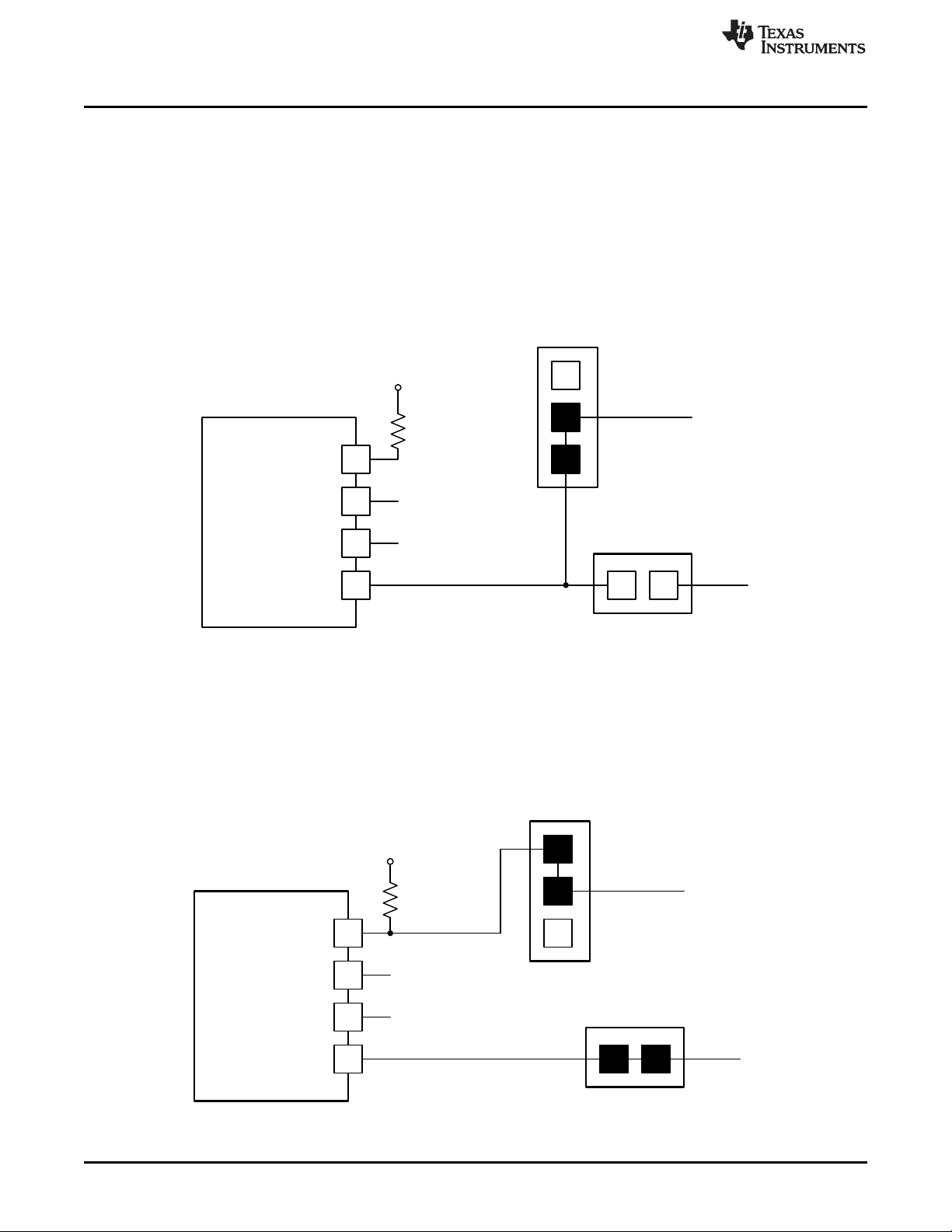
6.1 SPI 3-Wire Mode (JP2:2–3 and JP3:OPEN)
The chip-select signal is used to bring the ADS8860 digital output out of 3-state and initializes
conversions. The rising edge of the chip-select signal starts a conversion, then after the conversion time,
the falling edge of the chip-select signal brings the digital output out of 3-state. Figure 4 shows the serial
configuration for this mode.
www.ti.com
Figure 4. Serial 3-Wire Configuration
6.2 SPI 4-Wire Mode (JP2:1–2 and JP3:CLOSED)
The chip-select signal is used to bring the ADS8860 digital output out of 3-state. However, conversion is
initialized from J3:17 as an independent signal. The rising edge of J3:17 (CONVST) starts a conversion,
then after the conversion time, the falling edge of the chip-select signal brings the digital output out of 3state. Figure 5 shows the serial configuration for this mode.
8
Figure 5. Serial 4-Wire Configuration
ADS8860EVM-PDK SBAU213–September 2013
Copyright © 2013, Texas Instruments Incorporated
Submit Documentation Feedback
Page 9

www.ti.com
7 PDK Kit Setup
Do not connect the ADS8860EVM-PDK to a PC before completing Section 7.
Failure to observe this caution may cause Microsoft Windows to disregard the
ADS8860EVM-PDK as a connected device.
This section presents the steps required to setup the ADS8860EVM-PDK kit before operation. Section 8
explains how to operate the kit to acquire and analyze data.
The steps to setup the kit are as follows and must be completed before attempting to capture data:
Step 1. Download and install the ADCPro software (if not already installed) on a PC.
Step 2. Download and install the ADS8860EVM-PDK EVM plug-in software.
Step 3. Configure the ADS8860EVM-PDK hardware.
Step 4. Power-up the ADS8860EVM-PDK.
Each task is described in the subsequent sections of this document.
7.1 Installing the ADCPro Software
ADCPro is the primary program used to evaluate the ADS8860. ADCPro is available at
www.ti.com/tool/adcpro. Refer to the ADCPro User's Guide (SBAU128) for detailed installation
instructions.
PDK Kit Setup
CAUTION
7.2 Installing ADS8860EVM-PDK Plug-In Software
NOTE: ADCPro should be installed before attempting to install the ADS8860EVM-PDK plug-in
software.
The installation file link for the PDK plug-in can be found in the ADS8860EVM-PDK product folder at
www.ti.com/tool/ADS8860evm-pdk. In the software section, look for a link with a file named ads886x-
adcproplugin-<version #>.exe (<version #> refers to the installation file version number, and increments
with software version releases). Download and double-click the file to run it; then follow the instructions as
shown.
Figure 6 shows the initial and completed installer screen shots.
Figure 6. Plug-In Installer
SBAU213–September 2013 ADS8860EVM-PDK
Submit Documentation Feedback
Copyright © 2013, Texas Instruments Incorporated
9
Page 10

PDK Kit Setup
7.3 Configuring the ADS8860EVM-PDK Hardware
The ADS8860EVM-PDK contains both the ADS8860EVM and the MMB0 motherboard; however, the
devices may be shipped unconnected or configured incorrectly. Follow these steps to verify that the
ADS8860EVM-PDK kit is properly configured and connected:
Step 1. Unpack the ADS8860EVM-PDK kit.
Step 2. Set J12 to closed, J13A to open, and J13B to closed on the MMB0, as shown in Figure 7.
• J12 must be closed. This setting allows the wall supply to power-up the MMB0 and
ADS8860EVM through J2 (6-VDC input), and regulate down to 5 V, 3.3 V.
• J13B must be closed. This setting connects the 5-V analog power supply with the 5-V
digital power supply.
• J13A must be opened. This setting allows the 5-V analog power supply to be regulated
on board.
www.ti.com
Figure 7. MMB0 Motherboard Jumper Configuration
Step 3. Set JP1:2–3, JP2:2–3, JP3:open, and JP4:closed on the ADS8860EVM, as shown in
Figure 8.
Figure 8. ADS8860EVM Jumper Configuration
10
ADS8860EVM-PDK SBAU213–September 2013
Copyright © 2013, Texas Instruments Incorporated
Submit Documentation Feedback
Page 11

www.ti.com
4. Plug the ADS8860EVM into the MMB0.
Do not misalign the pins when plugging the ADS8860EVM into the MMB0.
Check the pin alignment carefully before applying power to the PDK.
7.4 Powering up the ADS8860EVM-PDK
When the ADS8860EVM-PDK kit is configured, power can be applied to the MMB0. This power comes
from a wall supply that delivers 6 VDC to the MMB0 through J2 on the MMB0 motherboard. This wall
power supply is included with the PDK.
After the power supply is connected, four green light-emitting diodes (LEDs) in the bottom right-hand
corner of the MMB0 motherboard should light up. If these LEDs do not light up, disconnect the power and
verify that J12 is closed on the MMB0 motherboard.
8 PDK Kit Operation
The evaluation software is based on ADCPro. This program operates with a variety of plug-ins. To use
ADCPro, load an EVM plug-in and a test plug-in (select these plug-ins from the EVM and test menus,
respectively). To unload a plug-in, select the unload option from the corresponding menu.
The following sections describe how to use ADCPro and the ADS8860EVM plug-in to acquire data.
PDK Kit Operation
CAUTION
8.1 About MMB0
The MMB0 provides the USB interface between the PC and the ADS8860EVM. The MMB0 is a modular
EVM system motherboard. The MMB0 is designed around the TMS320VC5509, a DSP with an onboard
USB interface from Texas Instruments. The MMB0 also has 16 MB of SDRAM installed.
The MMB0 is not sold as a DSP development board, and is not available separately. TI cannot offer
support for the MMB0 except as part of an EVM kit. For schematics or other information about the MMB0,
contact Texas Instruments.
8.2 Loading the ADS8860EVM-PDK Plug-in
Step 1. Make sure the PDK kit is configured and powered up, as explained in Section 7. Then, press
the Reset button on the MMB0 (in the top right-hand corner) one time to clear the board
memory.
Step 2. Connect the MMB0 to a PC with the USB cable provided with the kit.
Step 3. Start ADCPro from the Windows Start menu.
Step 4. Load the ADS886XEVM plug-in from the ADCPro drop-down EVM menu, as shown in
Figure 9. Note that only one EVM plug-in can be loaded at a time. If a different plug-in is
selected, the previous plug-in is unloaded.
Figure 9. Loading EVM Plug-in
SBAU213–September 2013 ADS8860EVM-PDK
Submit Documentation Feedback
Copyright © 2013, Texas Instruments Incorporated
11
Page 12

PDK Kit Operation
Step 5. When the plug-in is loaded, the plug-in searches for the board. A series of messages in the
status area indicates this action, eventually displaying Connected to EVM.
Step 6. Change the device name from ADS8861 to ADS8860.
The plug-in is now loaded and ready to function with the ADS8860EVM.
8.3 Using the ADS8860EVM Plug-in
The ADS8860EVM allows the user to evaluate the ADS8860 ADC. Figure 10 shows the device
configuration tab of the ADS8860EVM plug-in that is used to change acquisition parameters, such as
sample rate and voltage reference.
www.ti.com
Figure 10. ADS8860EVM Plug-in: Device Configuration Tab
The device configuration tab contains the following controls:
1. Data rate: By default, data rate is at 1 MSPS. This control shows the data rate or sampling frequency
used by the ADC to acquire data. With an SCLK frequency of 80 MHz, data rate can be set to a value
from 19.536 kSPS to 1 MSPS. With an SCLK frequency of 10 MHz, data rate can be set to a value
from 4 kSPS to 344.827 kSPS.
2. SCLK: By default, SCLK is at 80 MHz. SCLK sets the clock frequency used by the SPI interface to
capture data. SCLK should be a value between 70 MHz to 80 MHz for 1 MSPS. For slow sampling
rates, use 10 MHz. Do not use SCLK frequencies between 30 MHz and 50 MHz.
3. Reference: 4.5 V is the default reference value, which matches the onboard reference of the EVM.
The value of this control should always match the reference used by the ADC to read accurate
voltages.
4. Device selection: ADS8861 is the default device selected. Therefore, this value must be changed to
ADS8860 in order to match the ADS8860EVM.
5. About: This control shows the plug-in version, MMB0 firmware version, assembly date, and board
revision information. Note that the device name is ADS8881 because the software is based on the
ADS8881EVM.
6. Collection bar: This feature shows the percentage of data collected during an acquisition session.
12
ADS8860EVM-PDK SBAU213–September 2013
Copyright © 2013, Texas Instruments Incorporated
Submit Documentation Feedback
Page 13

www.ti.com
8.4 Loading Test Plug-in
When the ADS8860EVM plug-in is configured, one of the four test plug-ins must be loaded to acquire data
by using the drop-down Test menu, as shown in Figure 11. Note that only one Test plug-in can be loaded
at a time. If a different plug-in is selected, the previous plug-in is unloaded.
There are four different test options available for the ADS8860EVM:
• Data monitor: This test option acquires and exports data in a table format as hexadecimal data.
• MultiFFT: This test option allows the user to acquire data and create an FFT graph of power versus
frequency to display data.
• MultiHistogram: This option acquires data and creates a histogram of code values.
• MultiScope: This feature acquires and displays data in a graph of voltage versus time.
For further details regarding how to set up and use the various test plug-ins, refer to the ADCPro User's
Guide (SBAU128).
PDK Kit Operation
Figure 11. ADCPro Test Plug-ins
8.5 Acquiring Data
When the ADS8860EVM is configured for the desired test scenario, press the Acquire button to start the
data collection process; the software collects the number of data points specified in the Test plug-in Block
Size control. During data acquisition, the ADS8860EVM plug-in disables all front-panel controls and the
collection process bar displays the completion progress.
8.6 Troubleshooting
If the ADS8860EVM plug-in cannot find the ADS8860EVM-PDK, press the RESET button on the MMB0
and try again.
If ADCPro stops responding while the ADS8860EVM-PDK is connected, shut down and restart the
ADCPro software. Also, try unplugging the USB cable from the PDK.
SBAU213–September 2013 ADS8860EVM-PDK
Submit Documentation Feedback
Copyright © 2013, Texas Instruments Incorporated
13
Page 14

Bill of Materials, Schematics, and Layout
9 Bill of Materials, Schematics, and Layout
The bill of materials is provided in Table 5. Section 9.2 shows the PCB layouts for the ADS8860EVM.
Section 9.3 shows the schematic for the ADS8860EVM.
9.1 Bill of Materials
NOTE: All components should be compliant with the European Union Restriction on Use of
Hazardous Substances (RoHS) directive. Some part numbers may be either leaded or
RoHS. Verify that purchased components are RoHS-compliant. (For more information about
TI's position on RoHS compliance, refer to www.ti.com.)
Table 5. ADS8860EVM Bill of Materials
Item No. Qty Value Ref Des Description Manufacturer Part Number
1 1 — Printed Circuit Board, 3.2 in x 1.7 In. x 0.062 Texas 6548605
2 9 1 µF C1, C4, C5, C7, C10, Capacitor, X7R Ceramic +/-10%, 25WV, 0603 Murata GRM188R71E105KA12D
3 5 0.1 µF C2, C8, C11, C13, C21 Capacitor, X7R Ceramic +/-10%, 25WV, 0603 Murata GRM188R71E104KA01D
4 1 10000 pF C3 Capacitor, C0G Ceramic +/-5%, 50WV, 0603 TDK C1608C0G1H103J
5 3 10 µF C6, C9, C14 Capacitor, X7R Ceramic +/-10%, 10WV, 0805 Murata GRM21BR71A106KE51L
6 3 1000 pF C15, C17, C20 Capacitor, C0G Ceramic +/-5%, 50WV, 0603 Murata GRM1885C1H102JA01D
7 2 10 µF C16, C18 Capacitor, X7R Ceramic +/-10%, 16WV, 1206 TDK C3216X7R1C106K
8 2 — J1, J2 (Top) Header 20 Pin SMT Plug, .100" Gold (2x10) Samtec TSM-110-01-L-DV-P
9 2 — J1, J2 (Bottom) Header 20 Pin SMT Socket, .100" Gold (2x10) Samtec SSW-110-22-F-D-VS-K
10 1 — J3 (Top) Header 10 Pin SMT Plug, .100" Gold (2x5) Samtec TSM-105-01-L-DV-P
11 1 — J3 (Bottom) Header 10 Pin SMT Socket, .100" Gold (2x5) Samtec SSW-105-22-F-D-VS-K
12 1 — J4 CONN SMA JACK STRAIGHT PCB Amphenol 132134
13 2 — JP1, JP2 Header Strip, 3 pin .100" Gold (1x3) Samtec TSW-103-07-L-S
14 2 — JP3, JP4 Header Strip, 2 pin .100" Gold (1x2) Samtec TSW-102-07-L-S
15 6 — R1, R14, R16, R27, Not Installed — —
16 2 1k R2, R3 Resistor, Metal Film Chip, 0.1%, 1/10W, 0603 Panasonic ERA-3AEB102V
17 1 100 R4 Resistor, Thick Film Chip, 1%, 1/10W, 0603 Panasonic ERJ-3EKF1000V
18 2 4.7 R5, R6 Resistor, Thick Film Chip, 1%, 1/10W, 0603 Vishay/Dale CRCW06034R70FKEA
19 3 0.22 R7, R10, R17 Resistor, Thin Film Chip, 1%, 1/5W, 0603 Susumu RL0816S-R22-F
20 2 1k R8, R33 Resistor, Thick Film Chip, 1%, 1/10W, 0603 Panasonic ERJ-3EKF1001V
21 2 10 R9, R18 Resistor, Thick Film Chip, 1%, 1/10W, 0603 Vishay/Dale CRCW060310R0FKEA
22 3 20k R11, R12, R32 Resistor, Metal Film Chip, 0.1%, 1/10W, 0603 Panasonic ERA-3AEB203V
23 1 10k R13 Resistor, Metal Film Chip, 0.1%, 1/10W, 0603 Panasonic ERA-3AEB103V
24 4 0 R15, R21, R26, R28 Resistor, Thick Film Chip, 1/10W, 0603 Panasonic ERJ-3GEY0R00V
25 5 47 R19, R20, R22, R23, Resistor, Thick Film Chip, 1%, 1/10W, 0603 Panasonic ERJ-3EKF47R0V
26 2 10k R24, R25 Resistor, Thick Film Chip, 1%, 1/10W, 0603 Panasonic ERJ-3EKF1002V
27 1 — U1 IC ADC 16BIT 1MSPS PSEUDO-DIFF 10- Texas ADS8860IDGS
28 1 — U2 IC OPAMP VFB R-R 95MHZ SOT23-5 Texas THS4281DBV
29 1 — U3 IC LDO RGLTR 3.3V LN SOT-23-5 Texas TPS78833DBV
30 1 — U4 IC OPAMP VFB RRO 205MHZ SOT23-6 Texas OPA836IDBV
31 1 — U5 IC VREF SERIES PREC 4.5V 8-MSOP Texas REF5045IDGK
32 1 — U6 IC OPAMP GP 5.5MHZ SGL SOT23-5 Texas OPA376AIDBV
33 1 — U7 IC EEPROM 256KBIT 400KHZ 8TSSOP Microchip 24LC256-I/ST
34 1 — U8 IC OPAMP CHOP R-R 350KHZ SOT23-5 Texas OPA333AIDBV
C12, C19, C22, C23
R29, R30
R31
in. Instruments
MSOP Instruments
Instruments
Instruments
Instruments
Instruments
Instruments
Instruments
www.ti.com
14
ADS8860EVM-PDK SBAU213–September 2013
Copyright © 2013, Texas Instruments Incorporated
Submit Documentation Feedback
Page 15

www.ti.com
9.2 Board Layouts
Figure 12 through Figure 15 show the PCB layouts for the ADS8860EVM.
NOTE: Board layouts are not to scale. These figures are intended to show how the board is laid out;
they are not intended to be used for manufacturing ADS8860EVM PCBs.
Bill of Materials, Schematics, and Layout
Figure 12. ADS8860EVM PCB: Top Layer
Figure 13. ADS8860EVM PCB: Ground Layer
SBAU213–September 2013 ADS8860EVM-PDK
Submit Documentation Feedback
Copyright © 2013, Texas Instruments Incorporated
15
Page 16

Bill of Materials, Schematics, and Layout
Figure 14. ADS8860EVM PCB: Power Layer
www.ti.com
16
Figure 15. ADS8860EVM PCB: Bottom Layer
ADS8860EVM-PDK SBAU213–September 2013
Copyright © 2013, Texas Instruments Incorporated
Submit Documentation Feedback
Page 17

www.ti.com
9.3 Schematic
Bill of Materials, Schematics, and Layout
SBAU213–September 2013 ADS8860EVM-PDK
Submit Documentation Feedback
Copyright © 2013, Texas Instruments Incorporated
17
Page 18

Evaluation Board/Kit Important Notice
Texas Instruments (TI) provides the enclosed product(s) under the following conditions:
This evaluation board/kit is intended for use for ENGINEERING DEVELOPMENT, DEMONSTRATION, OR EVALUATION PURPOSES
ONLY and is not considered by TI to be a finished end-product fit for general consumer use. Persons handling the product(s) must have
electronics training and observe good engineering practice standards. As such, the goods being provided are not intended to be complete
in terms of required design-, marketing-, and/or manufacturing-related protective considerations, including product safety and environmental
measures typically found in end products that incorporate such semiconductor components or circuit boards. This evaluation board/kit does
not fall within the scope of the European Union directives regarding electromagnetic compatibility, restricted substances (RoHS), recycling
(WEEE), FCC, CE or UL, and therefore may not meet the technical requirements of these directives or other related directives.
Should this evaluation board/kit not meet the specifications indicated in the User’s Guide, the board/kit may be returned within 30 days from
the date of delivery for a full refund. THE FOREGOING WARRANTY IS THE EXCLUSIVE WARRANTY MADE BY SELLER TO BUYER
AND IS IN LIEU OF ALL OTHER WARRANTIES, EXPRESSED, IMPLIED, OR STATUTORY, INCLUDING ANY WARRANTY OF
MERCHANTABILITY OR FITNESS FOR ANY PARTICULAR PURPOSE.
The user assumes all responsibility and liability for proper and safe handling of the goods. Further, the user indemnifies TI from all claims
arising from the handling or use of the goods. Due to the open construction of the product, it is the user’s responsibility to take any and all
appropriate precautions with regard to electrostatic discharge.
EXCEPT TO THE EXTENT OF THE INDEMNITY SET FORTH ABOVE, NEITHER PARTY SHALL BE LIABLE TO THE OTHER FOR ANY
INDIRECT, SPECIAL, INCIDENTAL, OR CONSEQUENTIAL DAMAGES.
TI currently deals with a variety of customers for products, and therefore our arrangement with the user is not exclusive.
TI assumes no liability for applications assistance, customer product design, software performance, or infringement of patents or
services described herein.
Please read the User’s Guide and, specifically, the Warnings and Restrictions notice in the User’s Guide prior to handling the product. This
notice contains important safety information about temperatures and voltages. For additional information on TI’s environmental and/or
safety programs, please contact the TI application engineer or visit www.ti.com/esh.
No license is granted under any patent right or other intellectual property right of TI covering or relating to any machine, process, or
combination in which such TI products or services might be or are used.
FCC Warning
This evaluation board/kit is intended for use for ENGINEERING DEVELOPMENT, DEMONSTRATION, OR EVALUATION PURPOSES
ONLY and is not considered by TI to be a finished end-product fit for general consumer use. It generates, uses, and can radiate radio
frequency energy and has not been tested for compliance with the limits of computing devices pursuant to part 15 of FCC rules, which are
designed to provide reasonable protection against radio frequency interference. Operation of this equipment in other environments may
cause interference with radio communications, in which case the user at his own expense will be required to take whatever measures may
be required to correct this interference.
EVM Warnings and Restrictions
It is important to operate this EVM within the input voltage range of and the output voltage range of .
Exceeding the specified input range may cause unexpected operation and/or irreversible damage to the EVM. If there are questions
concerning the input range, please contact a TI field representative prior to connecting the input power.
Applying loads outside of the specified output range may result in unintended operation and/or possible permanent damage to the EVM.
Please consult the EVM User's Guide prior to connecting any load to the EVM output. If there is uncertainty as to the load specification,
please contact a TI field representative.
During normal operation, some circuit components may have case temperatures greater than . The EVM is designed to operate properly
with certain components above as long as the input and output ranges are maintained. These components include but are not limited to
linear regulators, switching transistors, pass transistors, and current sense resistors. These types of devices can be identified using the
EVM schematic located in the EVM User's Guide. When placing measurement probes near these devices during operation, please be
aware that these devices may be very warm to the touch.
Mailing Address: Texas Instruments, Post Office Box 655303, Dallas, Texas 75265
Copyright © 2013, Texas Instruments Incorporated
Page 19

IMPORTANT NOTICE
Texas Instruments Incorporated and its subsidiaries (TI) reserve the right to make corrections, enhancements, improvements and other
changes to its semiconductor products and services per JESD46, latest issue, and to discontinue any product or service per JESD48, latest
issue. Buyers should obtain the latest relevant information before placing orders and should verify that such information is current and
complete. All semiconductor products (also referred to herein as “components”) are sold subject to TI’s terms and conditions of sale
supplied at the time of order acknowledgment.
TI warrants performance of its components to the specifications applicable at the time of sale, in accordance with the warranty in TI’s terms
and conditions of sale of semiconductor products. Testing and other quality control techniques are used to the extent TI deems necessary
to support this warranty. Except where mandated by applicable law, testing of all parameters of each component is not necessarily
performed.
TI assumes no liability for applications assistance or the design of Buyers’ products. Buyers are responsible for their products and
applications using TI components. To minimize the risks associated with Buyers’ products and applications, Buyers should provide
adequate design and operating safeguards.
TI does not warrant or represent that any license, either express or implied, is granted under any patent right, copyright, mask work right, or
other intellectual property right relating to any combination, machine, or process in which TI components or services are used. Information
published by TI regarding third-party products or services does not constitute a license to use such products or services or a warranty or
endorsement thereof. Use of such information may require a license from a third party under the patents or other intellectual property of the
third party, or a license from TI under the patents or other intellectual property of TI.
Reproduction of significant portions of TI information in TI data books or data sheets is permissible only if reproduction is without alteration
and is accompanied by all associated warranties, conditions, limitations, and notices. TI is not responsible or liable for such altered
documentation. Information of third parties may be subject to additional restrictions.
Resale of TI components or services with statements different from or beyond the parameters stated by TI for that component or service
voids all express and any implied warranties for the associated TI component or service and is an unfair and deceptive business practice.
TI is not responsible or liable for any such statements.
Buyer acknowledges and agrees that it is solely responsible for compliance with all legal, regulatory and safety-related requirements
concerning its products, and any use of TI components in its applications, notwithstanding any applications-related information or support
that may be provided by TI. Buyer represents and agrees that it has all the necessary expertise to create and implement safeguards which
anticipate dangerous consequences of failures, monitor failures and their consequences, lessen the likelihood of failures that might cause
harm and take appropriate remedial actions. Buyer will fully indemnify TI and its representatives against any damages arising out of the use
of any TI components in safety-critical applications.
In some cases, TI components may be promoted specifically to facilitate safety-related applications. With such components, TI’s goal is to
help enable customers to design and create their own end-product solutions that meet applicable functional safety standards and
requirements. Nonetheless, such components are subject to these terms.
No TI components are authorized for use in FDA Class III (or similar life-critical medical equipment) unless authorized officers of the parties
have executed a special agreement specifically governing such use.
Only those TI components which TI has specifically designated as military grade or “enhanced plastic” are designed and intended for use in
military/aerospace applications or environments. Buyer acknowledges and agrees that any military or aerospace use of TI components
which have not been so designated is solely at the Buyer's risk, and that Buyer is solely responsible for compliance with all legal and
regulatory requirements in connection with such use.
TI has specifically designated certain components as meeting ISO/TS16949 requirements, mainly for automotive use. In any case of use of
non-designated products, TI will not be responsible for any failure to meet ISO/TS16949.
Products Applications
Audio www.ti.com/audio Automotive and Transportation www.ti.com/automotive
Amplifiers amplifier.ti.com Communications and Telecom www.ti.com/communications
Data Converters dataconverter.ti.com Computers and Peripherals www.ti.com/computers
DLP® Products www.dlp.com Consumer Electronics www.ti.com/consumer-apps
DSP dsp.ti.com Energy and Lighting www.ti.com/energy
Clocks and Timers www.ti.com/clocks Industrial www.ti.com/industrial
Interface interface.ti.com Medical www.ti.com/medical
Logic logic.ti.com Security www.ti.com/security
Power Mgmt power.ti.com Space, Avionics and Defense www.ti.com/space-avionics-defense
Microcontrollers microcontroller.ti.com Video and Imaging www.ti.com/video
RFID www.ti-rfid.com
OMAP Applications Processors www.ti.com/omap TI E2E Community e2e.ti.com
Wireless Connectivity www.ti.com/wirelessconnectivity
Mailing Address: Texas Instruments, Post Office Box 655303, Dallas, Texas 75265
Copyright © 2013, Texas Instruments Incorporated
Page 20

Mouser Electronics
Authorized Distributor
Click to View Pricing, Inventory, Delivery & Lifecycle Information:
Texas Instruments:
ADS8860EVM-PDK
 Loading...