Texas Instruments CD74HCT390E, CD74HCT390M96, CD74HCT390M, CD74HC390E, CD74HC390M96 Datasheet
...
CD74HC390,
/
j
[ /Title
(CD74
HC390
,
CD74
HCT39
0)
Subect
(High
Speed
CMOS
Data sheet acquired from Harris Semiconductor
SCHS185
September 1997
Features
• Two BCD Decade or Bi-Quinary Counters
• One Package Can Be Configured to Divide-by-2, 4,
5,10, 20, 25, 50 or 100
• Two Master Reset Inputs to Clear Each Decade
Counter Individually
• Fanout (Over Temperature Range)
- Standard Outputs. . . . . . . . . . . . . . . 10 LSTTL Loads
- Bus Driver Outputs . . . . . . . . . . . . . 15 LSTTL Loads
• Wide Operating Temperature Range . . . -55
• Balanced Propagation Delay and Transition Times
• Significant Power Reduction Compared to LSTTL
Logic ICs
• HC Types
- 2V to 6V Operation
- High Noise Immunity: N
= 30%, NIH = 30% of V
IL
at VCC = 5V
• HCT Types
- 4.5V to 5.5V Operation
- Direct LSTTL Input Logic Compatibility,
V
= 0.8V (Max), VIH = 2V (Min)
IL
- CMOS Input Compatibility, I
≤ 1µA at VOL, V
l
o
C to 125oC
CC
OH
CD74HCT390
High Speed CMOS Logic
Dual Decade Ripple Counter
Description
The Harris CD74HC390 and CD574HCT390 dual 4-bit
decade ripple counters are high-speed silicon-gate CMOS
devices and are pin compatible with low-power Schottky TTL
(LSTTL). These devices are divided into four separately
clocked sections. The counters have two divide-by-2 sections and two divide-by-5 sections. These sections are normally used in a BCD decade or bi-quinary configuration,
since they share a common master reset (nMR). If the two
master reset inputs (1MR and 2MR) are used to simultaneously clear all 8 bits of the counter, a number of counting
configurations are possible within one package. The separate clock inputs (n
ple counter or frequency division applications of divide-by-2,
4. 5, 10, 20, 25, 50 or 100. Each section is triggered by the
High-to-Low transition of the input pulses (n
For BCD decade operation, the nQ0 output is connected to
the n
CP1 input of the divide-by-5 section. For bi-quinary
decade operation, the nO3 output is connected to the n
input and nQ
The master reset inputs (1MR and 2MR) are active-High
asynchronous inputs to each decade counter which operates on the portion of the counter identified by the “1” and “2”
prefixes in the pin configuration. A High level on the nMR
input overrides the clock and sets the four outputs Low.
Ordering Information
CP0 and nCP1) of each section allow rip-
CP0 and nCP1).
becomes the decade output.
0
CP0
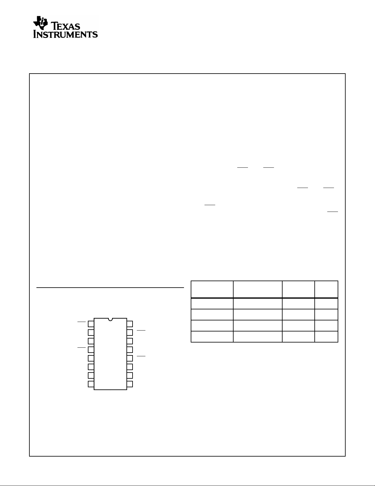
Pinout
CD74HC390, CD74HCT390
TOP VIEW
16
1
1CP0
1MR
2
1Q
3
0
4
1CP1
1Q
5
1
6
1Q
2
1Q
7
3
8
GND
CAUTION: These devices are sensitive to electrostatic discharge. Users should follow proper IC Handling Procedures.
Copyright
© Harris Corporation 1997
V
CC
15
2CP0
14
2MR
13
2Q0
12
2CP1
11
2Q
1
10
2Q
2
9
2Q
3
PART NUMBER TEMP. RANGE (oC) PACKAGE
CD74HC390E -55 to 125 16 Ld PDIP E16.3
CD74HCT390E -55 to 125 16 Ld PDIP E16.3
CD74HC390M -55 to 125 16 Ld SOIC M16.15
CD74HCT390M -55 to 125 16 Ld SOIC M16.15
NOTES:
1. When ordering, use the entire partnumber. Add the suffix 96 to
obtain the variant in the tape and reel.
2. Wafer for this part number is available which meets all electrical
specifications. Please contact your local sales office or Harris
customer service for ordering information.
1
PKG.
NO.
File Number 1838.2

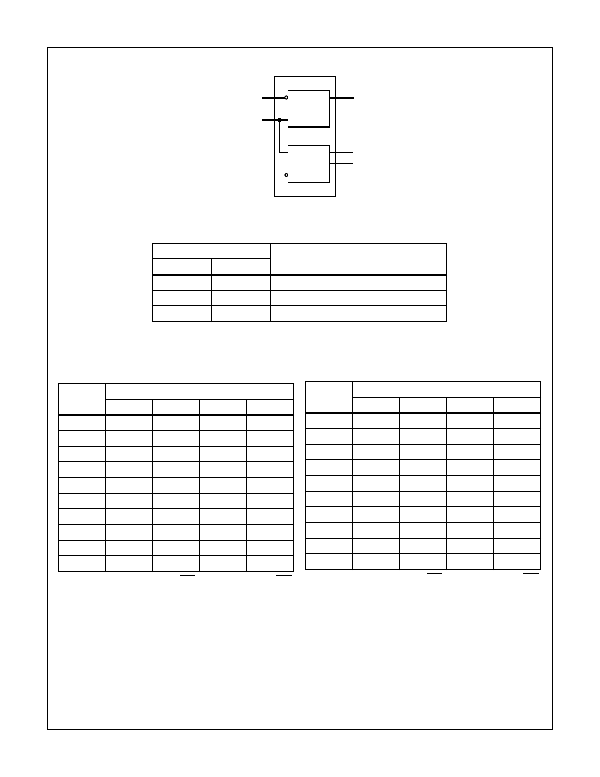
Functional Diagram
CD74HC390, CD74HCT390
1 (15)
nCP0
2 (14)
nMR
4 (12)
nCP1
GND = 8
V
= 16
CC
TRUTH TABLE
INPUTS
↑ L No Change
↓ L Count
X H All Qs Low
NOTE: H = High Voltage Level, L = Low Voltage Level, X = Don’t Care,
↑ = Transition from Low to High Level, ↓ = Transition from High to Low.
BCD COUNT SEQUENCE FOR 1/2 THE 390
OUTPUTS
COUNT
Q0 Q1 Q2 Q3
0LLLL
1HLLL
2LHLL
3HHLL
4LLHL
5HLHL
6LHHL
7HHHL
8LLLH
9HLLH
NOTE: Output nQ0 connected to nCP1 with counter input on nCP0.
3 (13)
nQ
nQ
nQ
nQ
0
1
2
3
÷ 2
COUNTER
÷ 5
COUNTER
5 (11)
6 (10)
7 (9)
ACTIONCP MR
B-QUINARY COUNT SEQUENCE FOR 1/2 THE 390
OUTPUTS
COUNT
Q0 Q1 Q2 Q3
0LLLL
1LHLL
2LLHL
3LHHL
4LLLH
5HLLL
6HHHL
7HLHL
8HHHL
9HLLH
NOTE: Output nQ3 connected to nCP0 with counter input on nCP1.
2

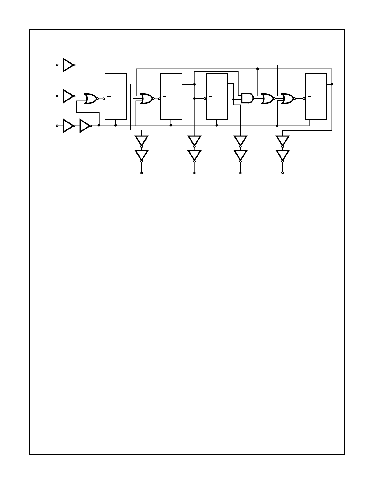
Logic Diagram
4(12)
CP1
n
CD74HC390, CD74HCT390
n
CP0
nMR
1(15)
2(14)
Q
Φ
R
3(13) 6(10) 7(9)
nQ
0
Q
Φ
R
5(11)
nQ
1
Q
Φ
R
VCC= 16
GND = 8
nQ
2
nQ
3
Q
Φ
R
3
 Loading...