Texas Instruments 5962-8995701VA, 5962-89957012A Datasheet

The UC1637 i s a p ul se width modulator circuit intended to be us ed for a variety of
PWM motor drive and amplifier applications requiring either uni-directional or bidirectional drive circuits. When used to replace conventional drivers, this circuit
can increase efficiency and reduce component costs for many applications. All
necessary circuitr y is included to generate an analog error signal and modulate
two bi-direc tional pulse train outpu ts in propor tion to the error signal magnitude
and polarity.
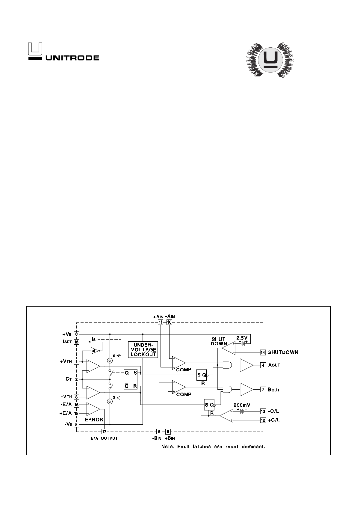
This monolithic device contains a sawtooth oscillator, error amplifier, and two
PWM compar ators with ±100mA output stages as standard features. Protection
circuitry includes under-voltage lockout, pulse-by-pulse current limiting, and a
shutdown port with a 2.5V temperature compensated threshold.
The UC1637 is characterized for operation over the full military temperature range
of -55°C to +125°C, while the UC2637 and UC3637 are characterized for -25°C to
+85°C and 0°C to +70°C, respectively.
Switched Mode Controller for DC Motor Drive
UC1637
UC2637
UC3637
BLOCK DIAGRAM
• Single or Dual Supply
Operation
•
±
2.5V to ±20V Input Supply
Range
•
±
5% Initial Oscillator
Accuracy; ± 10% Over
Temperature
• Pulse-by-Pulse Current
Limiting
• Under-Voltage Lockout
• Shutdown Input with
Temperature Compensated
2.5V Threshold
• Uncommitted PWM
Comparators for Design
Flexibility
• Dual 100mA, Source/Sink
Output Drivers
Supply Voltage (±Vs) . . . . . . . . . . . . . . . . . . . . . . . . . . . . . . . . . . . . . . . . . . . . . . . . . . . ±20V
Output Current, Source/Sink (Pins 4, 7) . . . . . . . . . . . . . . . . . . . . . . . . . . . . . . . . . . . 500mA
Analog Inputs (Pins 1, 2, 3, 8, 9, 10, 11 12, 13, 14, 15, 16) . . . . . . . . . . . . . . . . . . . . . . . ±Vs
Error Amplifier Output Current (Pin 17) . . . . . . . . . . . . . . . . . . . . . . . . . . . . . . . . . . . ±20mA
Oscillator Charging Current (Pin 18). . . . . . . . . . . . . . . . . . . . . . . . . . . . . . . . . . . . . . . -2mA
Power Dissipation at TA = 25°C (Note 2) . . . . . . . . . . . . . . . . . . . . . . . . . . . . . . . . 1000mW
Power Dissipation at TC = 25°C (Note 2) . . . . . . . . . . . . . . . . . . . . . . . . . . . . . . . . 2000mW
Storage Temperature Range . . . . . . . . . . . . . . . . . . . . . . . . . . . . . . . . . . . -65°C to +150°C
Lead Temperature (Soldering, 10 Seconds). . . . . . . . . . . . . . . . . . . . . . . . . . . . . . . . +300°C
Note 1: Currents are positive into, negative out of the specified terminal.
Note 2: Consult Packaging Section of Databook for thermal limitations and considerations
of package.
FEATURES
ABSOLUTE MAXIMUM RATINGS (Note 1)
DESCRIPTION
6/97

UC1637
UC2637
UC3637
PACKAGE PIN
FUNCTION
FUNCTION PIN
+V
TH
1
C
T
2
-V
TH
3
A
OUT
4
-V
S
5
N/C 6
+V
S
7
B
OUT
8
+B
IN
9
-B
IN
10
-A
IN
11
+A
IN
12
+C/L 13
-C/L 14
SHUTDOWN 15
N/C 16
+E/A 17
-E/A 18
E/A
OUTPUT 19
I
SET
20
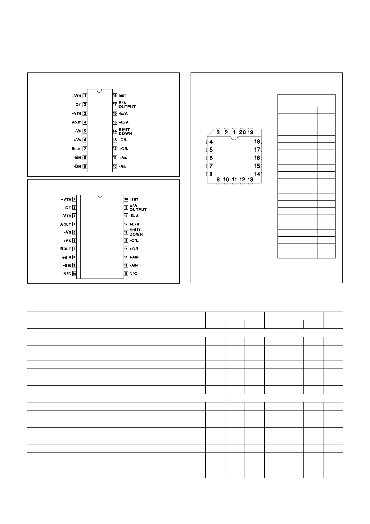
PLCC-20, LCC-20
(TOP VIEW)
Q, L Packages
ELECTRICAL CHARACTERISTICS:
PARAMETER TEST CONDITIONS UC1637/UC2637 UC3637 UNITS
MIN TYP MAX MIN TYP MAX
Oscillator
Initial Accuracy TJ = 25°C (Note 6) 9.4 10 10.6 9 10 11 kHz
Voltage Stability V
S
= ±5V to ±20V, V
PIN 1
= 3V,
V
PIN 3
= -3V
57 57%
Temperature Stability Over Operating Range (Note 3) 0.5 2 0.5 2 %
+V
TH
Input Bias Current V
PIN 2
= 6V -10 0.1 10 -10 0.1 10
µ
A
-V
TH
Input Bias Current V
PIN 2
= 0V -10 -0.5 -10 -0.5
µ
A
+V
TH,
-V
TH
Input Range +VS-2 -VS+2 +VS-2 -VS+2 V
Error Amplifier
Input Offset Voltage VCM = 0V 1.5 5 1.5 10 mV
Input Bias Current V
CM
= 0V 0.5 5 0.5 5
µ
A
Input Offset Current V
CM
= 0V 0.1 1 0.1 1
µ
A
Common Mode Range V
S
= ±2.5 to 20V -VS+2 +VS-VS+2 +V
S
V
Open Loop Voltage Gai n R
L
= 10k 75 100 80 100 dB
Slew Rate 15 15 V/
µ
S
Unity Gain Bandwidth 2 2 MHz
CMRR Over Common Mode Ra ng e 75 100 75 100 dB
PSRR VS = ±2.5 to ±20V 75 110 75 110 dB
CONNECTION DIAGRAM
Unless otherwise stated, these specifications apply for TA = -55°C to +125°C for the
UC1637; -25°C to +85°C for the UC2637; and 0°C to +70°C for the UC3637; +VS =
+15V, -VS = - 15V, +V
TH
= 5V, -V
TH
= -5V, RT = 16.7kΩ, CT = 1500pF, TA=T
J.
DIL-18 (TOP VIEW)
J or N Package
SOIC-20 (TOP VIEW)
DW Package
2

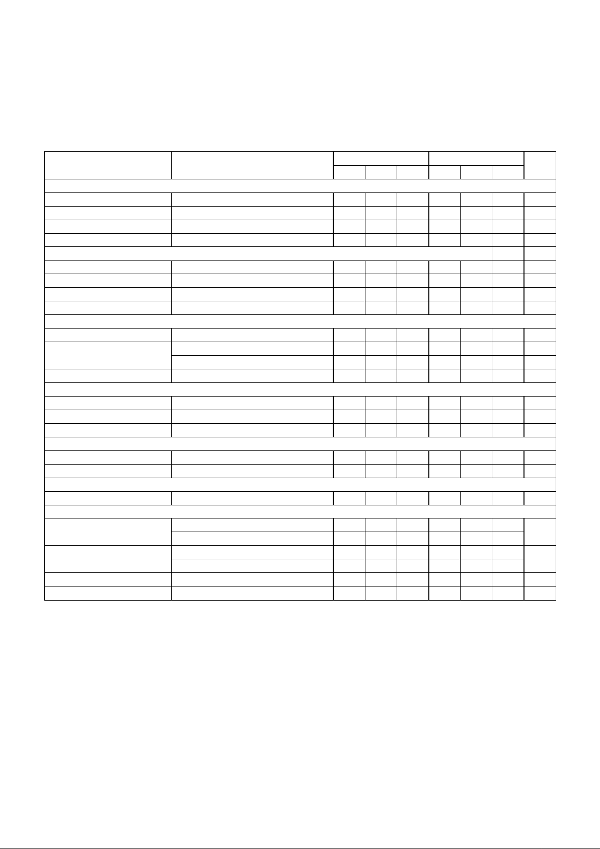
ELECTRICAL CHARACTERISTICS:
PARAMETERS TEST CONDITIONS UC1637/UC2637 UC3637 UNITS
MIN TYP MAX MIN TYP MAX
Error Amplifier (Continued)
Output Sink Current V
PIN 17
= 0V -50 -20 -50 -20 mA
Output Source Current V
PIN 17
= 0V 5 11 5 11 mA
High Level Output Voltage 13 13.6 13 13.6 V
Low Level Output V oltage -14.8 -13 -14.8 -13 V
PWM Comparators
Input Offset Voltage V
CM
= 0V 20 20 mV
Input Bias Current V
CM
= 0V 2 10 2 10
µ
A
Input Hysteresis V
CM
= 0V 10 10 mV
Common Mode range V
S
= ±5V to ±20V -VS+1 +VS-2 -VS+1 +VS-2 V
Current Limit
Input Offset Voltage V
CM
= 0V, TJ = 25°C 190 200 210 180 200 220 mV
Input Offset Voltage T.C. -0.2 -0.2 mV/°C
Input Bias Current -10 -1.5 -10 -1.5
µ
A
Common Mode Range V
S
= ±2.5V to ±20V -V
S
+VS-3 -V
S
+VS-3 V
Shutdown
Shutdown Threshold (Note 4) -2.3 -2.5 -2.7 -2.3 -2.5 -2.7 V
Hysteresis 40 40 mV
Input Bias Current V
PIN 14
= +VS to -V
S
-10 -0.5 -10 -0.5
µ
A
Under-Voltage Lockout
Start Threshold (Note 5) 4.15 5.0 4.15 5.0 V
Hysteresis 0.25 0.25 mV
Total Standby Current
Supply Current 8.5 15 8.5 15 mA
Output Section
Output Low Level I
SINK
= 20mA -14.9 -13 -14.9 -13 V
I
SINK
= 100mA -14.5 -13 -14.5 -13
Output High Level I
SOURCE
= 20mA 13 13.5 13 13.5 V
I
SOURCE
= 100mA 12 13.5 12 13.5
Rise Time (Note 3) C
L
= Inf, TJ = 25°C 100 600 100 600 ns
Fall Time (Note 3) C
L
= Inf, TJ = 25°C 100 300 100 300 ns
Note 3: These parameters, although guaranteed over the recommended operating conditions, are not 100% tested in production.
Note 4: Parameter measured with respect to +VS (Pin 6).
Note 5: Parameter measure d at +V
S
(Pin 6) with respect to -VS (Pin 5).
Note 6: R
T
and CT referenced to Ground.
UC1637
UC2637
UC3637
FUNCTIONAL DESCRIPTION
Following is a descr iption of each of the func tional blocks
shown in the Block Diagram.
Oscillator
The oscillator consists of two comparators, a charging
and discharg ing current source, a current source set ter minal, l
SET
and a flip- flop. The upper and lower threshold
of the oscilla tor waveform is set externally by applying a
voltage at pins +V
TH
and -VTH respectively. The +VTH ter-
minal voltage is buffered internally and also applied to the
l
SET
terminal to develop the capacitor charging current
through R
T
. If RT is referenced to -VS as shown in Figure
1, both the threshold voltage and charging current will
vary proportionally to the supply differential, and the oscillator frequency will remain constant. The triangle waveform oscillators frequency and voltage amplitude is
determ ined by the external components using the formulas
given in Figure 1.
Unless otherwise stated, these specifications apply for TA = -55°C to +125°C for the
UC1637; -25°C to +85°C for the UC2637; and 0°C to +70°C for the UC3637: VS =
+15V, -VS = - 15V, +V
TH
= 5V, -VTH = -5V, RT = 16.7kΩ, CT = 1500pF, TA=T
J.
3
 Loading...