

Texas Instruments 5962-89734012A Datasheet
SN54ACT04, SN74ACT04
HEX INVERTERS
SCAS518A – JULY 1995 – REVISED APRIL 1996
D
Inputs Are TTL-Voltage Compatible
D
EPIC
(Enhanced-Performance Implanted
CMOS) 1-µm Process
D
Package Options Include Plastic
Small-Outline (D), Shrink Small-Outline
(DB), Thin Shrink Small-Outline (PW), DIP
(N) Packages, Ceramic Chip Carriers (FK),
Flat (W), and DIP (J) Packages
description
The ‘ACT04 contain six independent inverters.
The devices perform the Boolean function Y = A
The SN54ACT04 is characterized for operation
over the full military temperature range of –55°C
to 125°C. The SN74ACT04 is characterized for
operation from –40°C to 85°C.
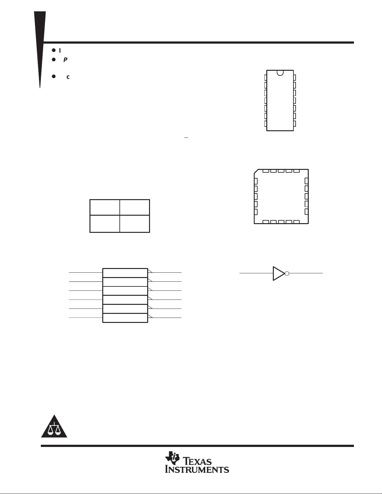
FUNCTION TABLE
(each inverter)
logic symbol
INPUT
A Y
H L
L H
†
OUTPUT
SN54ACT04 ...J OR W PACKAGE
SN74ACT04 . . . D, DB, N, OR PW PACKAGE
.
SN54ACT04 . . . FK PACKAGE
2A
NC
2Y
NC
3A
NC – No internal connection
(TOP VIEW)
1A
1
1Y
2
2A
3
2Y
4
3A
5
3Y
6
GND
7
(TOP VIEW)
1Y1ANC
3212019
4
5
6
7
8
910111213
3Y
GND
14
13
12
11
10
NC
V
CC
6A
6Y
5A
5Y
4A
9
4Y
8
CC
V
6A
18
17
16
15
14
4Y
4A
logic diagram, each inverter (positive logic)
6Y
NC
5A
NC
5Y
1
1A
3
2A 2Y
5
3A 3Y
9
4A 4Y
11
5A 5Y
13
6A 6Y
†
This symbol is in accordance with ANSI/IEEE Std 91-1984 and
IEC Publication 617-12.
Pin numbers shown are for the D, DB, J, N, PW, and W packages.
Please be aware that an important notice concerning availability, standard warranty, and use in critical applications of
Texas Instruments semiconductor products and disclaimers thereto appears at the end of this data sheet.
EPIC is a trademark of Texas Instruments Incorporated.
PRODUCTION DATA information is current as of publication date.
Products conform to specifications per the terms of Texas Instruments
standard warranty. Production processing does not necessarily include
testing of all parameters.
1
2
4
6
8
10
12
1Y
YA
Copyright 1996, Texas Instruments Incorporated
POST OFFICE BOX 655303 • DALLAS, TEXAS 75265
1
SN54ACT04, SN74ACT04
UNIT
HEX INVERTERS
SCAS518A – JULY 1995 – REVISED APRIL 1996
absolute maximum ratings over operating free-air temperature range (unless otherwise noted)
Supply voltage range, V
Input voltage range, VI (see Note 1) –0.5 V to VCC + 0.5 V. . . . . . . . . . . . . . . . . . . . . . . . . . . . . . . . . . . . . . . . . .
Output voltage range, VO (see Note 1) –0.5 V to VCC + 0.5 V. . . . . . . . . . . . . . . . . . . . . . . . . . . . . . . . . . . . . . .
Input clamp current, I
Output clamp current, I
Continuous output current, I
Continuous current through V
Maximum power dissipation at TA = 55°C (in still air) (see Note 2): D package 1.25 W. . . . . . . . . . . . . . . . . .
Storage temperature range, T
†
Stresses beyond those listed under “absolute maximum ratings” may cause permanent damage to the device. These are stress ratings only, and
functional operation of the device at these or any other conditions beyond those indicated under “recommended operating conditions” is not
implied. Exposure to absolute-maximum-rated conditions for extended periods may affect device reliability.
NOTES: 1. The input and output voltage ratings may be exceeded if the input and output current ratings are observed.
2. The maximum package power dissipation is calculated using a junction temperature of 150°C and a board trace length of 750 mils,
except for the N package, which has a trace length of zero.
–0.5 V to 7 V. . . . . . . . . . . . . . . . . . . . . . . . . . . . . . . . . . . . . . . . . . . . . . . . . . . . . . . . . .
CC
(V
< 0 or VI > VCC) ±20 mA. . . . . . . . . . . . . . . . . . . . . . . . . . . . . . . . . . . . . . . . . . . . . . . .
IK
I
(V
< 0 or V
OK
O
(VO = 0 to VCC) ±50 mA. . . . . . . . . . . . . . . . . . . . . . . . . . . . . . . . . . . . . . . . . . . . . .
O
or GND ±200 mA. . . . . . . . . . . . . . . . . . . . . . . . . . . . . . . . . . . . . . . . . . . . . . . . .
CC
> VCC) ±20 mA. . . . . . . . . . . . . . . . . . . . . . . . . . . . . . . . . . . . . . . . . . . .
O
DB package 0.5 W. . . . . . . . . . . . . . . . .
N package 1.1 W. . . . . . . . . . . . . . . . . . .
PW package 0.5 W. . . . . . . . . . . . . . . . .
–65°C to 150°C. . . . . . . . . . . . . . . . . . . . . . . . . . . . . . . . . . . . . . . . . . . . . . . . . .
stg
recommended operating conditions (see Note 3)
SN54ACT04 SN74ACT04
MIN MAX MIN MAX
V
CC
V
IH
V
IL
V
I
V
O
I
OH
I
OL
∆t/∆v Input transition rise or fall rate 0 8 0 8 ns/V
T
A
NOTE 3: Unused inputs must be held high or low to prevent them from floating.
Supply voltage 4.5 5.5 4.5 5.5 V
High-level input voltage 2 2 V
Low-level input voltage 0.8 0.8 V
Input voltage 0 V
Output voltage 0 V
High-level output current –24 –24 mA
Low-level output current 24 24 mA
Operating free-air temperature –55 125 –40 85 °C
CC
CC
0 V
0 V
CC
CC
V
V
†
2
POST OFFICE BOX 655303 • DALLAS, TEXAS 75265
 Loading...