UC1903
UC2903
UC3903
Quad Supply and Line Monitor
FEATURES
•
Inputs for Monitoring up to Four
Separate Supply Voltage Levels
•
Internal Inverter for Sensing a
Negative Supply Voltage
•
Line/Switch Sense Input for Early
Power Source Failure Warning
•
Programmable Under- and
Over-Voltage Fault Thresholds
with Proportional Hysteresis
•
A Precision 2.5V Reference
•
General Purpose Op-Amp for
Auxiliary Use
•
Three High Current, >30mA,
Open-Collector Outputs Indicate
Over-Voltage, Under-Voltage
and Power OK Conditions
•
Input Supply Under-Voltage
Sensing and Start-Latch
Eliminate Erroneous Fault Alerts
During Start-Up
•
8-40V Supply Operation with
7mA Stand-By Current
DESCRIPTION
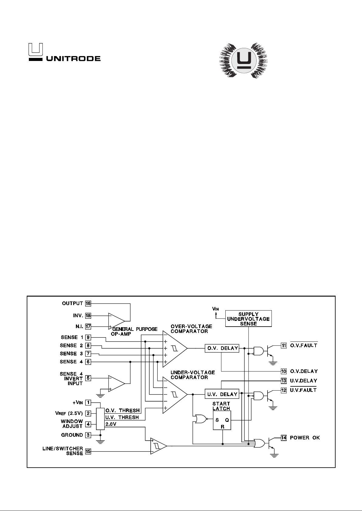
The UC1903 fam i l y of qu ad s up pl y a nd l ine monitor integrated circuits wil l respond to under- and over-voltage conditions on up to four continuously monitored volt age leve ls. An internal op-amp i nverte r allows at least one of these
levels to b e n egat iv e. A separate line/switcher sense input is available to provide early warning of line or other power source failures.
The fault window adjustment ci rcuit on these devices provides easy programming of un der- and ov er-voltage thr esholds. The thresholds, center ed around
a precision 2. 5V r e fe ren c e, ha ve a n i n pu t h y ste r esi s t ha t sc a l es with the window width for precise, glitch-free operation. A reference output pin allows the
sense input fault windo ws to be scal ed independen tly using simp le resistive
dividers.
The three open collector outputs on these devices will sink in excess of 30mA
of load current when activ e. The under- and over-voltage outputs respond after separate, user d efine d, d ela ys to r espect ive fa ult co nd itions. T h e t h ir d o u tput is active during any fault condition including under- and over-voltage,
line/switc her faul ts, and i nput sup ply unde r-volt age. The off s tate of this output indicates a "power OK" situation.
An additional, uncommitted, general purpose op-amp is also included. This
op-amp, capa ble of s ourc ing 20mA of output cu rr ent, can be used for a number of auxiliary functions including the sensing and amplification of a feedback error signal when the 2.5V output is used as a system reference.
In addition, these ICs are equipped with a start-latch to prevent erroneous under-voltage indications during start-up. These parts operate over an 8V to
40V input supply range and require a typical stand-by current of only 7mA.
BLOCK DIAGRAM
4/97
Note: Pin numbers refe r to J, N and D W pa ck ag es .

UC1903
UC2903
UC3903
Supply Voltage (+VIN) . . . . . . . . . . . . . . . . . . . . . . . . . . . . . +40V
Open Collector Output Voltages. . . . . . . . . . . . . . . . . . . . . +40V
Open Collector Output Currents. . . . . . . . . . . . . . . . . . . . 50mA
Sense 1-4 Input Voltages. . . . . . . . . . . . . . . . . . . -0.3V to +20V
Line/Switcher Sense Input Voltage . . . . . . . . . . . -0.3V to +40V
Op-Amp and Inverter Input Voltages . . . . . . . . . . -0.3V to +40V
Op-Amp and Inverter Output Currents . . . . . . . . . . . . . . -40mA
Window Adjust Voltage. . . . . . . . . . . . . . . . . . . . . 0.0V to +10V
Delay Pin Voltages . . . . . . . . . . . . . . . . . . . . . . . . . 0.0V to +5V
Reference Output Current . . . . . . . . . . . . . . . . . . . . . . . -40mA
Power Dissipation at T
A
= 25°C (Note 1) . . . . . . . . . . . 1000mW
Power Dissipation at TC = 25°C (Note 1) . . . . . . . . . . . 2000mW
Operating Junction Temperature . . . . . . . . . . . -55°C to +150°C
Storage Temperature . . . . . . . . . . . . . . . . . . . . -65°C to +150°C
Lead Temperature (Soldering, 10 Seconds) . . . . . . . . . . 300°C
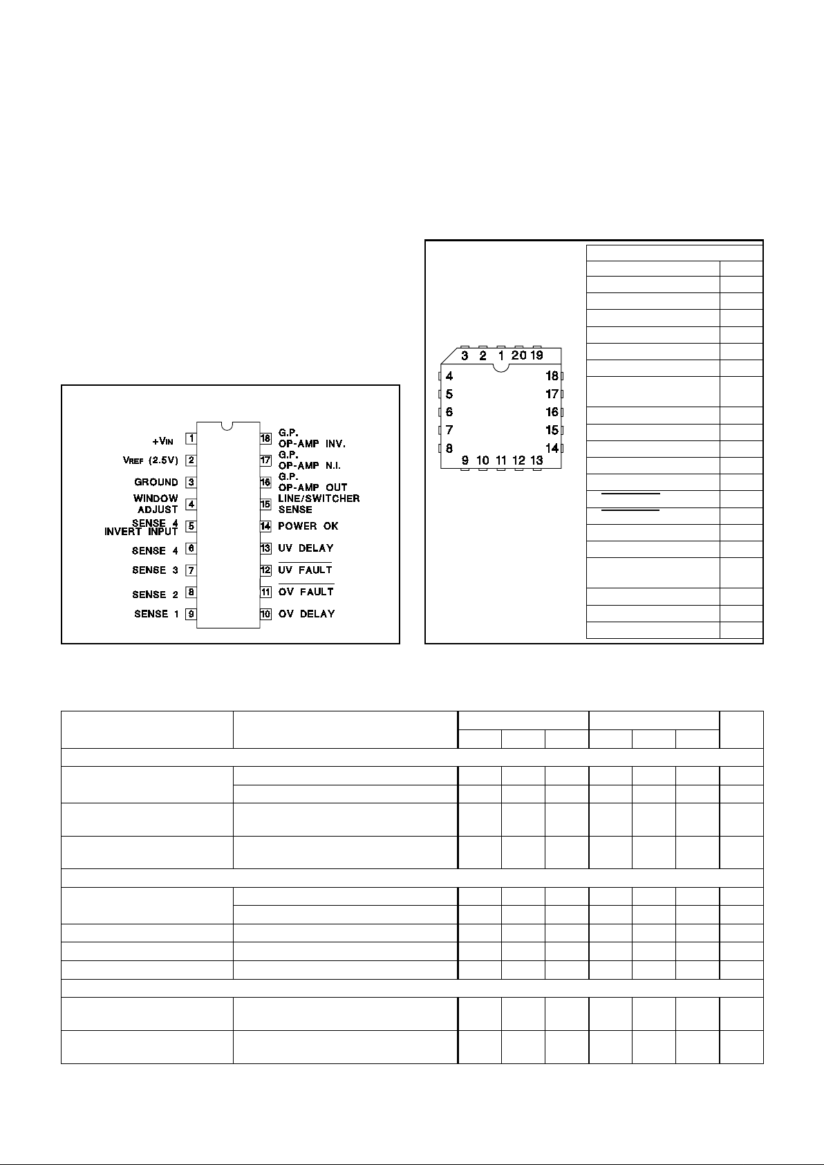
CONNECTION DIAGRAMS
DIL-18, SOIC-18 (TOP VIEW)
J or N, DW Package
PACKAGE PIN FUNCTION
FUNCTION PIN
+VIN 1
V
REF
(2.5V) 2
GROUND 3
GROUND 4
WINDOW ADJUST 5
N/C 6
SENSE 4 INVERT
INPUT
7
SENSE 4 8
SENSE 3 9
SENSE 2 10
SENSE 1 11
OV DELAY 12
OV FAULT 13
UV FAULT 14
UV DELAY 15
POWER OK 16
LINE/SWITCHER
SENSE
17
G.P. OP-AMP OUT 18
G.P. OP-AMP N.I. 19
G.P. OP-AMP INV. 20
PLCC-20, LCC-20
(TOP VIEW)
Q, L Package
ELECTRICAL CHARACTERISTICS:
Unless otherwise st ated, these specif ic at io ns app ly f or TA = –55°C to +125°C for the
UC1903; –40°C to +85°C for the UC2903; and 0°C to +70°C for the UC3903; +VIN =
15V; Sense Inputs (Pins 6–9 an d Pin 15) = 2. 5V; V
PIN 4
= 1.0V, TA = T
J.
PARAMETERS TEST CONDITIONS UC1903 / UC2903 UC3903 UNITS
MIN TYP MAX MIN TYP MAX
Supply
Input Supply Current No Faults 7 9 7 11 mA
UV, OV and Line Fau lt 10 15 10 18 mA
Supply Under Voltage
Threshold (V
SUV
)
Fault Outputs Enabled 6.0 7.0 7.5 5.5 7.0 8.0 V
Minimum Supply to Enable
Power OK Output
3.0 4.0 3.0 4.0 V
Reference
Output Voltage (V
REF
)T
J
= 25°C 2.485 2.5 2.515 2.470 2.5 2.530 V
Over Temperatur e 2.465 2.535 2.465 2.535 V
Load Regulation I
L
= 0 to 10mA 1 10 1 15 mV
Line Regulation +V
IN
= 8 to 40V 1 4 1 8 mV
Short Circuit Current TJ = 25°C 40 40 mA
Fault Thresholds (Note 4)
OV Threshold Adj. Offset from V
REF
as a function of V
PIN 4
Input = Low to High, 0.5V ≤ V
PIN 4
≤ 2.5V
.230 .25 .270 .230 .25 .270 V/V
UV Threshold Adj. Offset from V
REF
as a function of V
PIN 4
Input = High to Low, 0.5V ≤ V
PIN 4
≤ 2.5V
-.270 -.25 -.230 -.270 -.25 -.230 V/V
ABSOLUTE MAXIMUM RATINGS
(Note 1)
Note 1: Voltages are referenced to gro un d (Pin 3) . Curren ts
are positive into, negative out of, the specified terminals.
Consult Packaging Section of Databook for thermal
limitations and considerations of package.
2

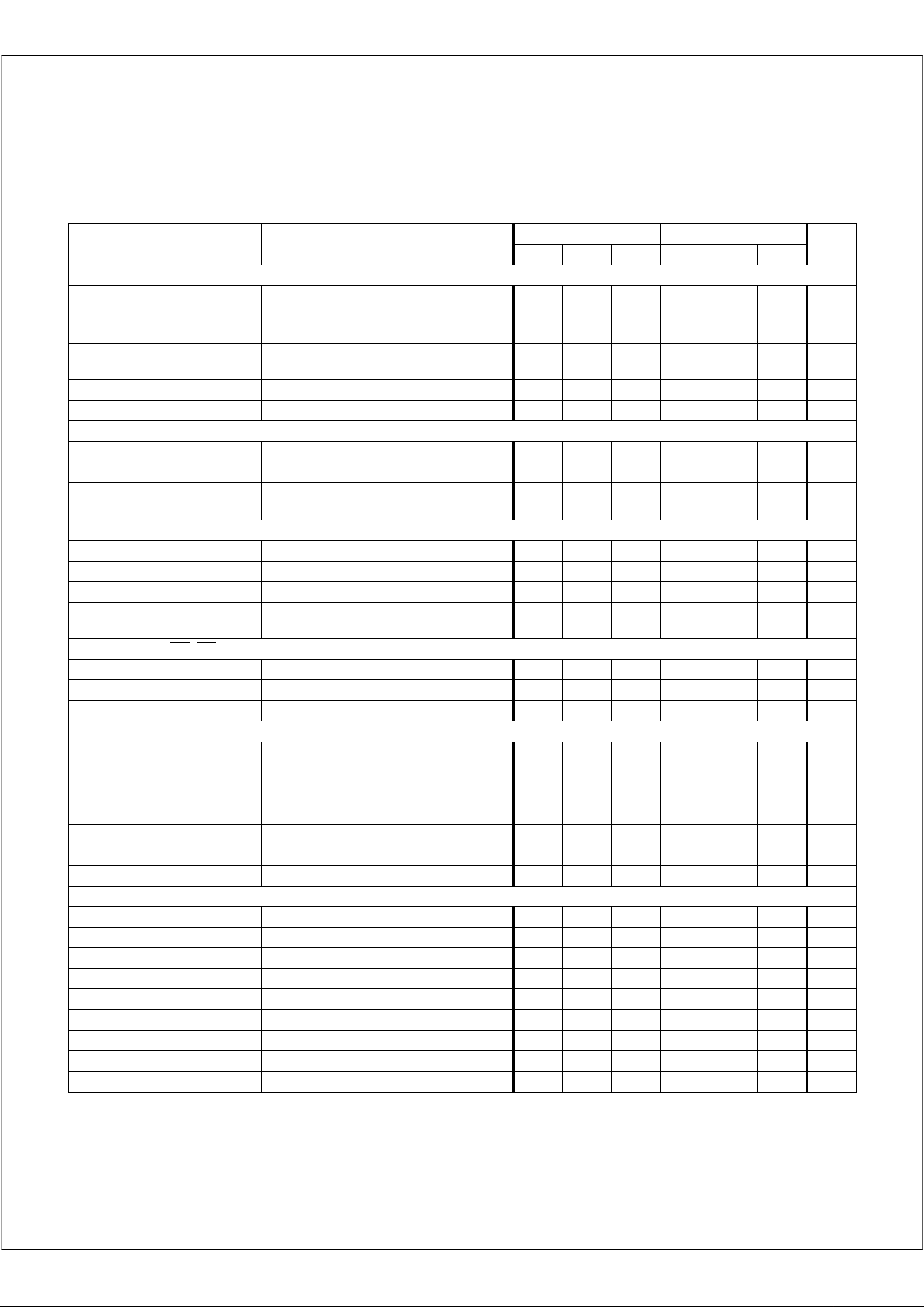
ELECTRICAL CHARACTERISTICS:
PARAMETERS TEST CONDITIONS UC1903/UC2903 UC3903 UNITS
MIN TYP MAX MIN TYP MAX
Fault Thresholds (cont.)
OV & UV Threshold Hyst. 0.5V ≤ V
PIN 4
≤ 2.5V 10 20 30 10 20 30 mV/V
OV & UV Threshold Supply
Sensitivity
+VIN = 8V to 40V .002 .01 .002 .02 %/V
Adjust Pin (Pin 4)
Input Bias Current
0.5V ≤ V
PIN 4
≤ 2.5V ±1 ±10 ±1 ±12 µA/V
Line Sense Threshold Input = High to Low 1.94 2.0 2.06 1.9 2.0 2.1 V
Line Sense Threshold Hyst. 125 175 225 100 175 250 mV
Sense Input s
Sense 1-4
Input Bias Current
Input = 2.8V (Note 2) 1 3 1 6 µA
Input = 2.2 (Note 2) -1 -3 -1 -6
µ
A
Line Sense Input
Bias Current
Input = 2.3V (Note 2) 1 3 1 6
µ
A
OV and UV Fault Delay
Charging Current 60 60 µA
Threshold Voltage Delay Pin = Low to High 1.8 1.8 V
Threshold Hysteresis T
J
= 25°C 250 250 mV
Delay Ratio of Threshold Voltage to Charging
Current
20 30 50 20 30 50 ms/µF
Fault Outputs (
OV, UV, & Power 0K)
Maximum Curre nt V
OUT
= 2V 30 70 30 70 mA
Saturation Voltage I
OUT
= 12mA .25 .40 .25 .40 V
Leakage Current V
OUT
= 40 V 3 25 3 25 µA
Sense 4 Inverter (Note 3)
Input Offset Voltage 2 8 2 10 mV
Input Bias Current .1 2 .1 4 µA
Open Loop Gain 65 80 65 80 d B
PSRR +V
IN
= 8 to 40 V 65 100 65 100 dB
Unity Gain Frequency 1 1 MHz
Slew Rate .4 .4 V/µs
Short Circuit Current T
J
= 25°C 40 40 mA
G.P. Op-Amp (Note 3)
Input Offset Voltage 1 5 1 8 mV
Input Bias Voltage .1 2 .1 4
µ
A
Input Offset Current .01 .5 .01 1.0 µA
Open Loop Gain 65 120 65 120 dB
CMRR V
CM
= 0 to +VIN = 2.0V 65 100 65 100 dB
PSRR +VIN = 8 to 40V 65 100 65 100 dB
Unity Gain Frequency 1 1 MHz
Slew Rate .4 .4 V/µs
Short Circuit Current T
J
= 25°C 40 40 mA
Note 2: These currents represent maximum input bias currents required as the sense inputs cross appropriate thresholds.
Note 3: When either the G.P. OP-Amp, or the Sense 4 Inverter, are configured for sensing a negative supply volta ge , th e di vi de r
resistance at the inverting input should be chosen such that the nominal divider current is
≤
1.4mA. With the divider current
at or below this level possible latching of the circuit is avoided. Proper operation for currents at or below 1.4mA is 100%
tested in produc ti on.
Note 4: Reference to pin numbers in this specification per tain to 18 pin DIL N and J packag es and 18 pin SOIC DW package.
UC1903
UC2903
UC3903
Unless otherwise st ated, these specif ic at io ns app ly f or TA = –55°C to +125°C for the
UC1903; –40°C to +85°C for the UC2903; and 0°C to +70°C for the UC3903; +VIN =
15V; Sense Inputs (Pins 6–9 an d Pin 15) = 2. 5V; V
PIN 4
= 1.0V, TA = T
J.
3
 Loading...