

UC1707
UC2707
UC3707
DESCRIPTION
The UC1707 family of power drivers is made with a high-speed Schottky
process to interface between low-level control functions and high-power
switching devices - particularly power MOSFETs. These devices contain
two independent channels, each of which can be activated by either a high
or low input logic level signal. Each output can source or sink up to 1.5A as
long as power dissipation limits are not exceeded.
Although each output can be activated independently with its own inputs, it
can be forced low in common through the action either of a digital high signal at the Shutdown terminal or a differential low-level analog signal. The
Shutdown command from either source can either be latching or not, depending on the status of the Latch Disable pin.
Supply voltage for both VIN and VC can independently range from 5V to
40V.
These devices are available in two-watt plastic "bat-wing" DIP for operation
over a 0°C to 70°C temperature range and, with reduced power, in a hermetically sealed cerdip for –55°C to +125°C operation. Also available in
surface mount DW, Q, L packages.
Dual Channel Power Driver
FEATURES
• Two independent Drivers
• 1.5A Totem Pole Outputs
• Inverting and Non-Inverting Inputs
• 40ns Rise and Fall into 1000pF
• High-Speed, Power MOSFET
Compatible
• Low Cross-Conduction Current Spike
• Analog Shutdown with Optional Latch
• Low Quiescent Current
• 5V to 40V Operation
• Thermal Shutdown Protection
• 16-Pin Dual-In-Line Package
• 20-Pin PLCC and CLCC Package
03/99
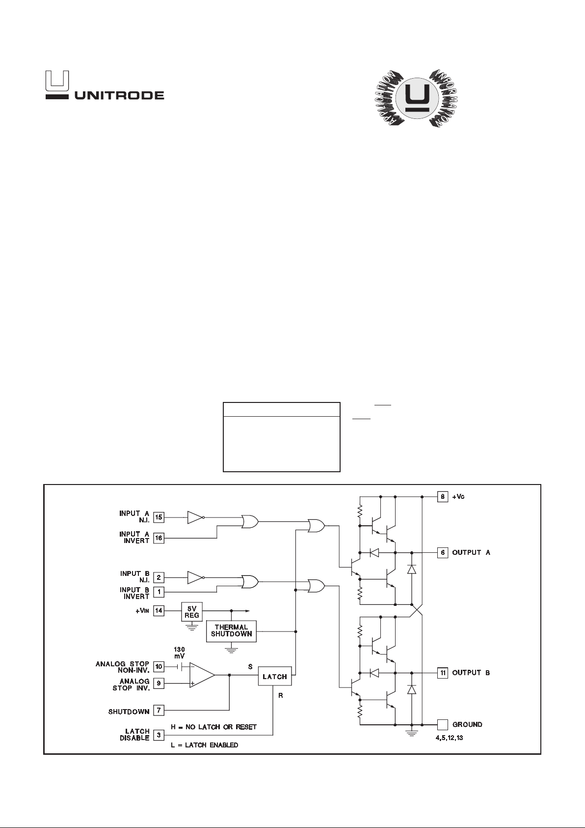
BLOCK DIAGRAM
INV. N.I. OUT OUT = INV and N.I.
H H L OUT
= INV or N.I.
LHH
HLL
LLL
TRUTH TABLE (Each Channel)
2
UC1707
UC2707
UC3707
Supply Voltage, VIN, N/J-Pkg . . . . . . . . . . . . . . . . . . . . . . . 40V
Collector Supply Voltage, VC, N/J-Pkg . . . . . . . . . . . . . . . 40V
Output Current (Each Output, Source or Sink) Steady-State,
N/J-Pkg. . . . . . . . . . . . . . . . . . . . . . . . . . . . . . . . . . . ±500mA
Peak Transient
N-Pkg . . . . . . . . . . . . . . . . . . . . . . . . . . . . . . . . . . . . . . ±1.5A
J-Pkg . . . . . . . . . . . . . . . . . . . . . . . . . . . . . . . . . . . . . . ±1.0A
Capacitive Discharge Energy
N-Pkg . . . . . . . . . . . . . . . . . . . . . . . . . . . . . . . . . . . . . . 20mJ
J-Pkg. . . . . . . . . . . . . . . . . . . . . . . . . . . . . . . . . . . . . . . 15mJ
Digital Inputs (See Note), N/J-Pkg . . . . . . . . . . . . . . . . . . . 5.5V
Analog Stop Inputs, N/J-Pkg . . . . . . . . . . . . . . . . . . . . . . . . VIN
Power Dissipation at TA= 25°C (See Note)
N-Pkg . . . . . . . . . . . . . . . . . . . . . . . . . . . . . . . . . . . . . . . . 2W
J-Pkg . . . . . . . . . . . . . . . . . . . . . . . . . . . . . . . . . . . . . . . . 1W
Power Dissipation at T (Leads/Case) = 25°C (See Note)
N-Pkg . . . . . . . . . . . . . . . . . . . . . . . . . . . . . . . . . . . . . . . . 5W
J-Pkg . . . . . . . . . . . . . . . . . . . . . . . . . . . . . . . . . . . . . . . . 2W
Operating Temperature Range. . . . . . . . . . . . –55°C to +125°C
Storage Temperature Range . . . . . . . . . . . . . –65°C to +150°C
Lead Temperature (Soldering, 10 Seconds) . . . . . . . . . . 300°C
ABSOLUTE MAXIMUM RATINGS
Note: All voltages are with respect to the four ground pins
which must be connected together. All currents are positive
into, negative out of the specified terminal. Digital Drive can exceed 5.5V if input current is limited to 10mA. Consult Packaging section of Databook for thermal limitations and
considerations of package.
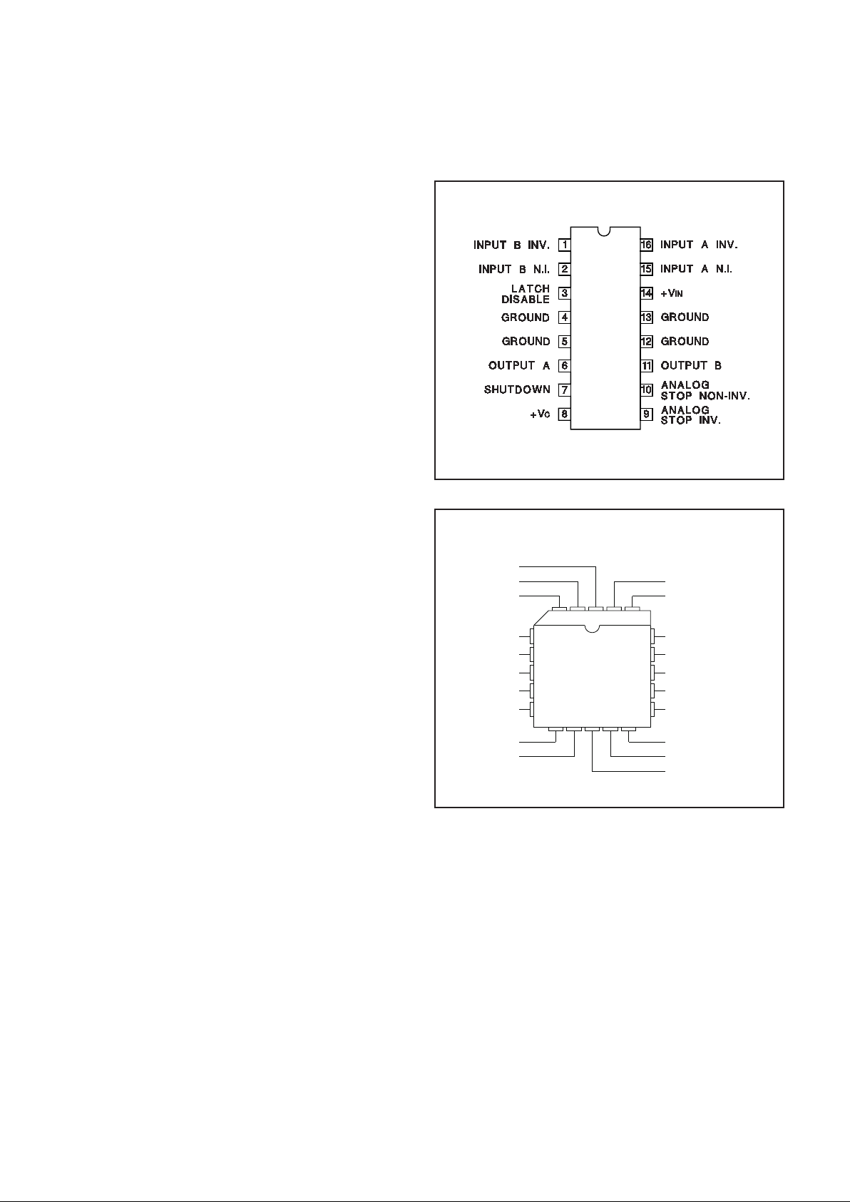
CONNECTION DIAGRAMS
DIL-16, SOIC-16 (TOP VIEW)
J or N Package,
3
18
17
16
N/C
122019
15
14
4
5
6
7
8
91110 12 13
INPUT B INV.
INPUT B I.N.
INPUT A INV.
INPUT A NON INV.
VIN
GROUND
N/C
GROUND
OUTPUT B
LATCH DISABLE
GROUND
N/C
GROUND
OUTPUT A
ANALOG STOP INV.
ANALOG STOP NON INV.
N/C
SHUTDOWN
VC
PLCC-20, LCC-20 (TOP VIEW)
Q, L Packages
Note: All four ground pins must be connected to a common
ground.
3
UC1707
UC2707
UC3707
ELECTRICAL CHARACTERISTICS:
Unless otherwise stated, these specifications apply for TA= –55°C to +125°C for
the UC1707, –25°C to +85°C for the UC2707 and 0°C to +70°C for the UC3707; VIN= VC= 20V. TA=TJ.
PARAMETERS TEST CONDITIONS MIN
TYP MAX UNITS
V
IN
Supply Current VIN= 40V 12 15 mA
V
C
Supply Current VC= 40V, Outputs Low 5.2 7.5 mA
V
C
Leakage Current VIN=0, VC =30V, No Load .05 0.1 mA
Digital Input Low Level 0.8 V
Digital Input High Level 2.2 V
Input Current V
I
= 0 –0.06 –1.0 mA
Input Leakage V
I
= 5V .05 0.1 mA
Output High Sat., V
C-VO
IO= –50mA 2.0 V
I
O
= –500mA 2.5 V
Output Low Sat., V
O
IO= –50mA 0.4 V
I
O
= –500mA 2.5 V
Analog Threshold V
CM
= 0 to 15V 100 130 160 mV
Input Bias Current V
CM
= 0 –10 –20 µA
Thermal Shutdown 155 °C
Shutdown Threshold Pin 7 Input 0.4 1.0 2.2 V
Latch Disable Threshold Pin 3 Input 0.8 1.2 2.2 V
TYPICAL SWITCHING CHARACTERISTICS: V
IN
= VC= 20V, TA= 25°C. Delays measured to 10% output change.
PARAMETERS TEST CONDITIONS
OUTPUT CL = UNITS
From Inv. Input to Output
open 1.0 2.2 nF
Rise Time Delay 40 50 60 ns
10% to 90% Rise 25 40 50 ns
Fall Time Delay 30 40 50 ns
90% to 10% Fall 25 40 50 ns
From N.I. Input to Output
Rise Time Delay 30 40 50 ns
10% to 90% Rise 25 40 50 ns
Fall Time Delay 45 55 65 ns
90% to 10% Fall 25 40 50 ns
V
C
Cross-Conduction
Current Spike Duration
Output Rise 25 ns
Output Fall 0 ns
Analog Shutdown Delay Stop non-Inv. = 0V 180 ns
Stop Inv. = 0 to 0.5V 180 ns
Digital Shutdown Delay 2V Input on Pin 7 50 ns

4
UC1707
UC2707
UC3707
The input zener may be used to clamp input signal voltages
higher than 5V as long as the zener current is limited to
10mA max. External pull-up resistors are not required.
SIMPLIFIED INTERNAL CIRCUITRY
Figure 1. Typical digital input gate.
Figure 3. Latch disable.
The Shutdown latch is disabled when pin 3 is open. An impedance of 4k or less from pin 3 to ground will allow a shutdown signal to set the latch which can then be reset by
either recycling the VIN supply or by momentarily (>200ns)
raising pin 3 high.
The input common-mode voltage range is from ground to (VIN-3V). When not used both inputs shoul1d be grounded. Activate
time is a function of overdrive with a typical value of 180ns. Pin 7 serves both as a comparator output and as a common digital
shutdown input. A high signal here will accomplish the fastest turn off of both outputs. Note that "OFF" is defined as the outputs
low.Pulling shutdown low defeats the latch operation regardless of its status.
Figure 2. Typical digital input gate.

5
UC1707
UC2707
UC3707
Figure 5. Current limiting.
The Analog shutdown can give pulse-by-pulse current limiting with a reset pulse from the clock output of the UC1524. R1C1 is
used to filter leading edge spikes.
SIMPLIFIED INTERNAL CIRCUITRY (cont.)
Figure 4. Transformer coupled push-pull MOSFET drive circuit.

6
UC1707
UC2707
UC3707
Figure 9. Power bipolar drive circuit.
D1, D2: UC3611 Schottky Diodes
Figure 6. Over-voltage protection.
APPLICATIONS
With an external reference, the shutdown comparator can
be used for over-voltage protection. R1 and R2 set the
shutdown level while R3 adds positive feedback for hysteresis.
Figure 7. Power MOSFET drive circuit.
D1, D2: UC3611 Schottky Diodes
Figure 8. Charge pump circuits.
When driven with a TTL square wave drive, the low output
impedance of the UC1707 allows ready implementation of
charge pump voltage converters.

7
UC1707
UC2707
UC3707
UNITRODE CORPORATION
7 CONTINENTAL BLVD.• MERRIMACK, NH 03054
TEL. (603) 424-2410 • FAX (603) 424-3460
Figure 11. Power MOSFET drive circuit using negative bias voltage and level shifting to ground reference
PWM.
D1, D2: UC3611 Schottky Diode
Figure 10. Transformer coupled MOSFET drive circuit.
TRANSFORMER COUPLING
D1, D2: UC3611 Schottky Diode

IMPORTANT NOTICE
T exas Instruments and its subsidiaries (TI) reserve the right to make changes to their products or to discontinue
any product or service without notice, and advise customers to obtain the latest version of relevant information
to verify, before placing orders, that information being relied on is current and complete. All products are sold
subject to the terms and conditions of sale supplied at the time of order acknowledgement, including those
pertaining to warranty, patent infringement, and limitation of liability.
TI warrants performance of its semiconductor products to the specifications applicable at the time of sale in
accordance with TI’s standard warranty. Testing and other quality control techniques are utilized to the extent
TI deems necessary to support this warranty. Specific testing of all parameters of each device is not necessarily
performed, except those mandated by government requirements.
CERT AIN APPLICATIONS USING SEMICONDUCTOR PRODUCTS MAY INVOLVE POTENTIAL RISKS OF
DEATH, PERSONAL INJURY, OR SEVERE PROPERTY OR ENVIRONMENTAL DAMAGE (“CRITICAL
APPLICATIONS”). TI SEMICONDUCTOR PRODUCTS ARE NOT DESIGNED, AUTHORIZED, OR
WARRANTED TO BE SUITABLE FOR USE IN LIFE-SUPPORT DEVICES OR SYSTEMS OR OTHER
CRITICAL APPLICATIONS. INCLUSION OF TI PRODUCTS IN SUCH APPLICA TIONS IS UNDERSTOOD T O
BE FULLY AT THE CUSTOMER’S RISK.
In order to minimize risks associated with the customer’s applications, adequate design and operating
safeguards must be provided by the customer to minimize inherent or procedural hazards.
TI assumes no liability for applications assistance or customer product design. TI does not warrant or represent
that any license, either express or implied, is granted under any patent right, copyright, mask work right, or other
intellectual property right of TI covering or relating to any combination, machine, or process in which such
semiconductor products or services might be or are used. TI’s publication of information regarding any third
party’s products or services does not constitute TI’s approval, warranty or endorsement thereof.
Copyright 1999, Texas Instruments Incorporated
 Loading...