

54AC16244, 74AC16244
16-BIT BUFFERS/LINE DRIVERS
WITH 3-STATE OUTPUTS
SCAS120A – MARCH 1990 – REVISED APRIL 1996
D
Members of the Texas Instruments
Widebus
D
3-State Outputs Drive Bus Lines or Buffer
t
Family
Memory Address Registers
D
Flow-Through Architecture Optimizes PCB
Layout
D
Distributed VCC and GND Configuration
Minimizes High-Speed Switching Noise
D
EPIC
t
(Enhanced-Performance Implanted
CMOS) 1-mm Process
D
500-mA Typical Latch-Up Immunity at
125°C
D
Package Options Include Plastic 300-mil
Shrink Small-Outline (DL) and Thin Shrink
Small-Outline (DGG) Packages Using 25-mil
Center-to-Center Pin Spacings, and 380-mil
Fine-Pitch Ceramic Flat (WD) Packages
Using 25-mil Center-to-Center Pin Spacings
description
The ’AC16244 are 16-bit buffers/line drivers
designed specifically to improve both the
performance and density of 3-state memory
address drivers, clock drivers, and bus-oriented
receivers and transmitters. They can be used as
four 4-bit buffers, two 8-bit buffers, or one 16-bit
buffer. These devices provide true outputs and
symmetrical active-low output-enable (OE
inputs. When OE is low, the device passes
noninverted data from the A inputs to the Y
outputs. When OE
high-impedance state.
is high, the outputs are in the
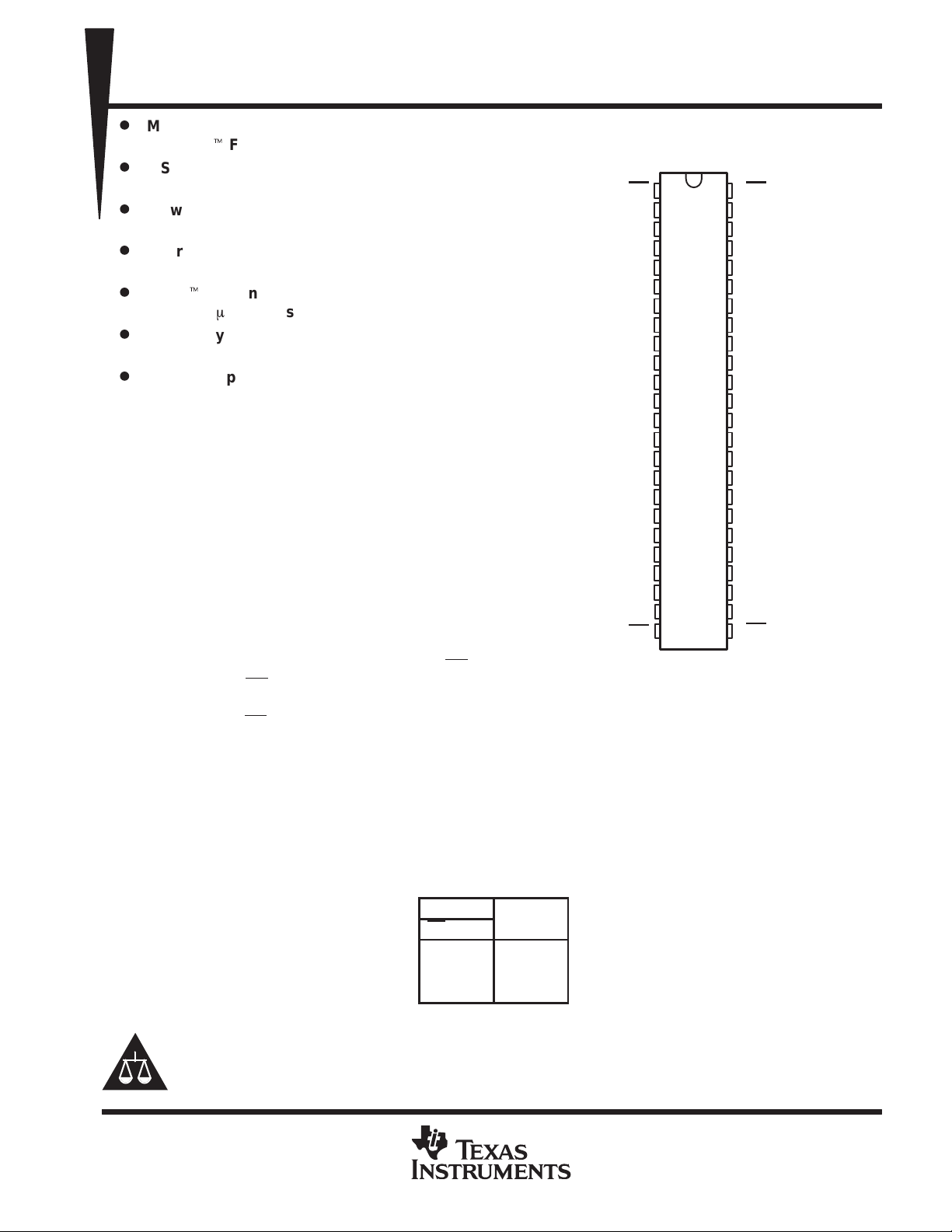
54AC16244 . . . WD PACKAGE
74AC16244 . . . DGG OR DL PACKAGE
1OE
1Y1
1Y2
GND
1Y3
1Y4
V
CC
2Y1
2Y2
GND
2Y3
2Y4
3Y1
3Y2
GND
3Y3
3Y4
V
CC
4Y1
4Y2
GND
4Y3
4Y4
4OE
(TOP VIEW)
1
48
2
47
3
46
4
45
5
44
6
43
7
42
8
41
9
40
10
39
11
38
12
37
13
36
14
35
15
34
16
33
17
32
18
31
19
30
20
29
21
28
22
27
23
26
24
25
2OE
1A1
1A2
GND
1A3
1A4
V
CC
2A1
2A2
GND
2A3
2A4
3A1
3A2
GND
3A3
3A4
V
CC
4A1
4A2
GND
4A3
4A4
3OE
)
The 74AC16244 is packaged in the TI’s shrink small-outline package, which provides twice the I/O pin count
and functionality of standard small-outline packages in the same printed-circuit-board area.
The 54AC16244 is characterized for operation over the full military temperature range of –55°C to 125°C. The
74AC16244 is characterized for operation from –40°C to 85°C.
FUNCTION TABLE
(each driver)
INPUTS
OE A
L H H
L LL
H X Z
Please be aware that an important notice concerning availability, standard warranty, and use in critical applications of
Texas Instruments semiconductor products and disclaimers thereto appears at the end of this data sheet.
EPIC and Widebus are trademarks of Texas Instruments Incorporated.
UNLESS OTHERWISE NOTED this document contains PRODUCTION
DATA information current as of publication date. Products conform to
specifications per the terms of Texas Instruments standard warranty.
Production processing does not necessarily include testing of all
parameters.
POST OFFICE BOX 655303 • DALLAS, TEXAS 75265
OUTPUT
Y
Copyright 1996, Texas Instruments Incorporated
1
54AC16244, 74AC16244
16-BIT BUFFERS/LINE DRIVERS
WITH 3-STATE OUTPUTS
SCAS120A – MARCH 1990 – REVISED APRIL 1996
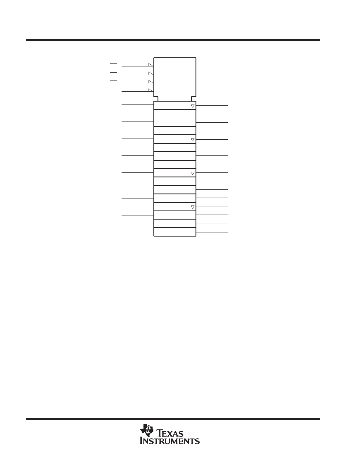
logic symbol
†
1
1OE
2OE
3OE
4OE
1A1
1A2
1A3
1A4
2A1
2A2
2A3
2A4
3A1
3A2
3A3
3A4
4A1
4A2
4A3
4A4
48
25
24
47
46
44
43
41
40
38
37
36
35
33
32
30
29
27
26
EN1
EN2
EN3
EN4
11
12
13
14
16
17
19
20
22
23
2
1Y1
3
1Y2
5
1Y3
6
1Y4
8
2Y1
9
2Y2
2Y3
2Y4
3Y1
3Y2
3Y3
3Y4
4Y1
4Y2
4Y3
4Y4
1
1
1
2
1
3
1
4
†
This symbol is in accordance with ANSI/IEEE Std 91-1984 and IEC Publication 617-12.
2
POST OFFICE BOX 655303 • DALLAS, TEXAS 75265
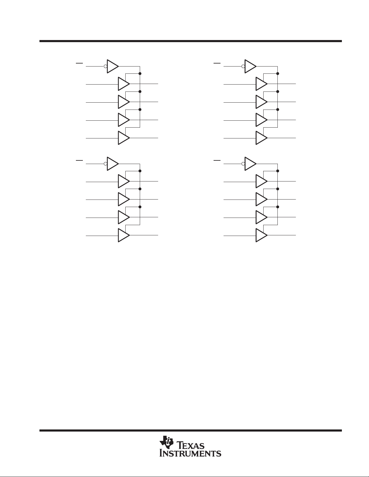
logic diagram (positive logic)
54AC16244, 74AC16244
16-BIT BUFFERS/LINE DRIVERS
WITH 3-STATE OUTPUTS
SCAS120A – MARCH 1990 – REVISED APRIL 1996
1OE
1A1
1A2
1A3
1A4
2OE
2A1
2A2
2A3
2A4
1
47
46
44
43
48
41
40
38
37
11
12
25
3OE
2
1Y1
3
1Y2
5
1Y3
6
1Y4
8
2Y1
9
2Y2
2Y3
2Y4
3A1
3A2
3A3
3A4
4OE
4A1
4A2
4A3
4A4
36
35
33
32
24
30
29
27
26
13
14
16
17
19
20
22
23
3Y1
3Y2
3Y3
3Y4
4Y1
4Y2
4Y3
4Y4
absolute maximum ratings over operating free-air temperature range (unless otherwise noted)
Supply voltage range, VCC –0.5 V to 7 V. . . . . . . . . . . . . . . . . . . . . . . . . . . . . . . . . . . . . . . . . . . . . . . . . . . . . . . . . .
Input voltage range, VI (see Note 1) –0.5 V to V
Output voltage range, VO (see Note 1) –0.5 V to V
Input clamp current, I
Output clamp current, I
Continuous output current, I
(V
< 0 or VI > VCC) ±20 mA. . . . . . . . . . . . . . . . . . . . . . . . . . . . . . . . . . . . . . . . . . . . . . . .
IK
I
(V
< 0 or VO > VCC) ±50 mA. . . . . . . . . . . . . . . . . . . . . . . . . . . . . . . . . . . . . . . . . . . .
OK
O
(V
= 0 to VCC) ±50 mA. . . . . . . . . . . . . . . . . . . . . . . . . . . . . . . . . . . . . . . . . . . . . .
O
O
Continuous current through VCC or GND ±400 mA. . . . . . . . . . . . . . . . . . . . . . . . . . . . . . . . . . . . . . . . . . . . . . . . . .
Maximum power dissipation at TA = 55°C (in still air) (see Note 2):DGG package 0.85 W. . . . . . . . . . . . . . . .
DL package 1.2 W. . . . . . . . . . . . . . . . . . .
Storage temperature range, T
†
Stresses beyond those listed under “absolute maximum ratings” may cause permanent damage to the device. These are stress ratings only, and
functional operation of the device at these or any other conditions beyond those indicated under “recommended operating conditions” is not
implied. Exposure to absolute-maximum-rated conditions for extended periods may affect device reliability.
NOTES: 1. The input and output voltage ratings may be exceeded if the input and output current ratings are observed.
2. The maximum package power dissipation is calculated using a junction temperature of 150°C and a board trace length of 750 mils.
–65°C to 150°C. . . . . . . . . . . . . . . . . . . . . . . . . . . . . . . . . . . . . . . . . . . . . . . . . . .
stg
CC
CC
+ 0.5 V. . . . . . . . . . . . . . . . . . . . . . . . . . . . . . . . . . . . . . . . . . .
+ 0.5 V. . . . . . . . . . . . . . . . . . . . . . . . . . . . . . . . . . . . . . . .
†
POST OFFICE BOX 655303 • DALLAS, TEXAS 75265
3
54AC16244, 74AC16244
UNIT
PARAMETER
TEST CONDITIONS
V
UNIT
I
mA
I
mA
pF
16-BIT BUFFERS/LINE DRIVERS
WITH 3-STATE OUTPUTS
SCAS120A – MARCH 1990 – REVISED APRIL 1996
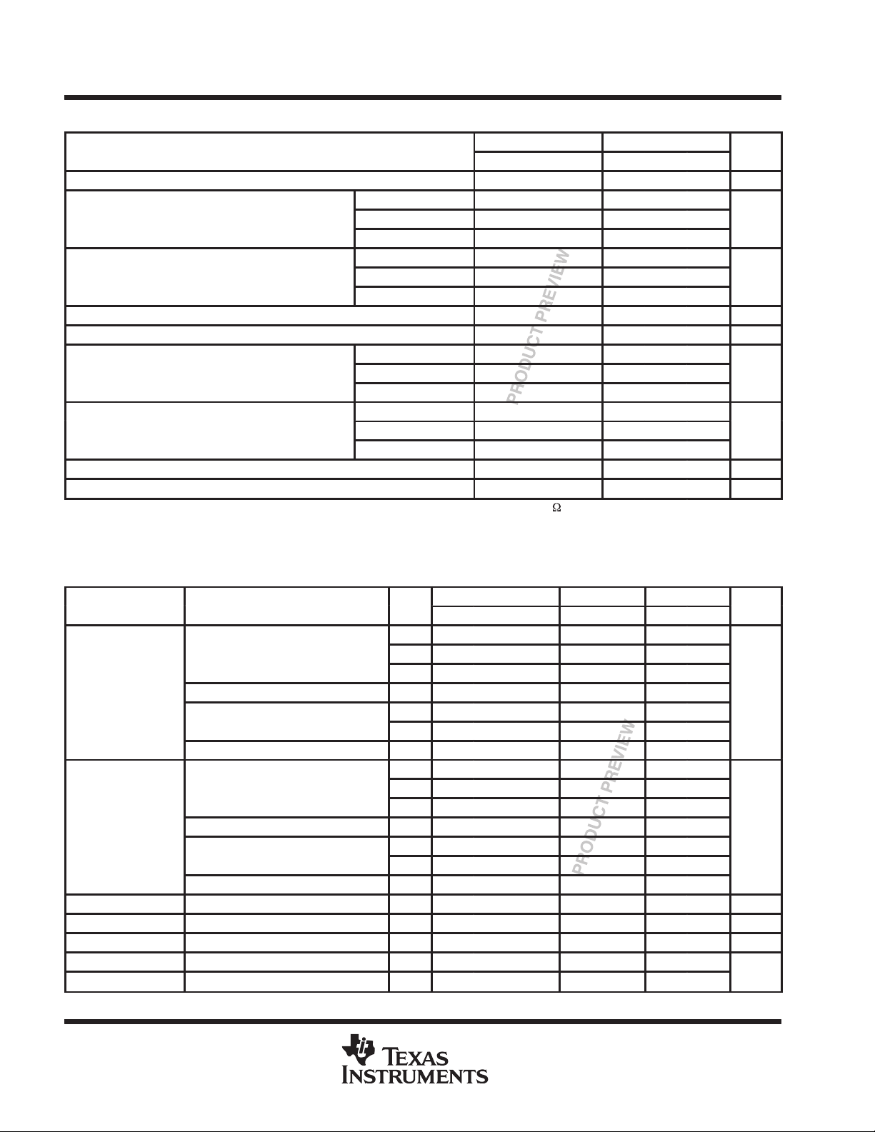
recommended operating conditions (see Note 3)
54AC16244 74AC16244
MIN NOM MAX MIN NOM MAX
V
V
V
V
V
I
OH
I
OL
∆t/∆v Input transition rise or fall rate 0 10 0 10 ns/V
T
NOTES: 3. Unused inputs should be tied to VCC through a pullup resistor of approximately 5 kW or greater to prevent them from floating.
Supply voltage (see Note 4) 3 5 5.5 3 5 5.5 V
CC
VCC = 3 V 2.1 2.1
High-level input voltage
IH
Low-level input voltage
IL
Input voltage 0 V
I
Output voltage 0 V
O
High-level output current
Low-level output current
Operating free-air temperature –55 125 –40 85 °C
A
4. All VCC and GND pins must be connected to the proper voltage supply.
VCC = 4.5 V
VCC = 5.5 V 3.85 3.85
VCC = 3 V 0.9 0.9
VCC = 4.5 V
VCC = 5.5 V 1.65 1.65
VCC = 3 V –4 –4
VCC = 4.5 V
VCC = 5.5 V –24 –24
VCC = 3 V 12 12
VCC = 4.5 V
VCC = 5.5 V 24 24
3.15 3.15
1.35 1.35
CC
CC
–24 –24
24 24
0 V
0 V
CC
CC
V
V
V
V
mA
mA
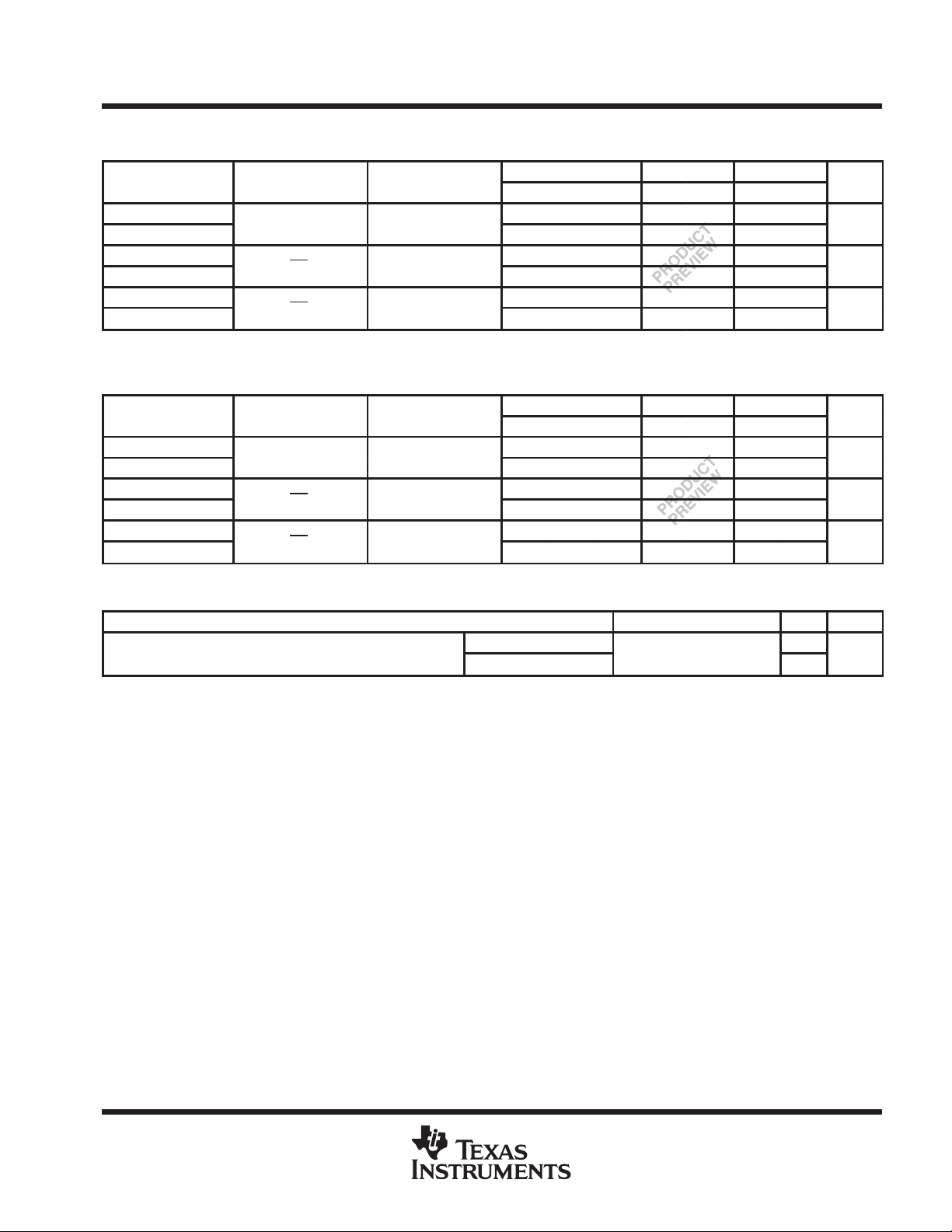
electrical characteristics over recommended operating free-air temperature range (unless
otherwise noted)
CC
3 V 2.9 2.9 2.9
IOH = –50 µA
V
OH
V
OL
I
I
I
OZ
I
CC
C
i
C
o
†
Not more than one output should be tested at a time, and the duration of the test should not exceed 10 ms.
IOH = –4 mA 3 V 2.58 2.48 2.48
= –24
OH
IOH = –75 mA
IOL = –50 µA
IOL = 12 mA 3 V 0.36 0.44 0.44
= 24
OL
IOL = 75 mA
VI = VCC or GND 5.5 V ±0.1 ±1 ±1 µA
VI = VCC or GND 5.5 V ±0.5 ±5 ±5 µA
VI = VCC or GND, IO = 0 5.5 V 8 80 80 µA
VI = VCC or GND 5 V 4.5
VI = VCC or GND 5 V 12
†
†
4.5 V 4.4 4.4 4.4
5.5 V 5.4 5.4 5.4
4.5 V 3.94 3.8 3.8
5.5 V 4.94 4.8 4.8
5.5 V 3.85 3.85
3 V 0.1 0.1 0.1
4.5 V 0.1 0.1 0.1
5.5 V 0.1 0.1 0.1
4.5 V 0.36 0.44 0.44
5.5 V 0.36 0.44 0.44
5.5 V 1.65 1.65
TA = 25°C 54AC16244 74AC16244
MIN TYP MAX MIN MAX MIN MAX
V
V
p
PRODUCT PREVIEW information concerns products in the formative or
design phase of development. Characteristic data and other
specifications are design goals. Texas Instruments reserves the right to
change or discontinue these products without notice.
4
POST OFFICE BOX 655303 • DALLAS, TEXAS 75265
PARAMETER
UNIT
A
Y
ns
OE
Y
ns
OE
Y
ns
PARAMETER
UNIT
A
Y
ns
OE
Y
ns
OE
Y
ns
CpdPower dissipation capacitance per latch
C
f
pF
54AC16244, 74AC16244
16-BIT BUFFERS/LINE DRIVERS
WITH 3-STATE OUTPUTS
SCAS120A – MARCH 1990 – REVISED APRIL 1996
switching characteristics over recommended operating free-air temperature range,
= 3.3 V ± 0.3 V (unless otherwise noted) (see Figure 1)
V
CC
FROM TO
(INPUT) (OUTPUT)
t
PLH
t
PHL
t
PZH
t
PZL
t
PHZ
t
PLZ
switching characteristics over recommended operating free-air temperature range,
V
= 5 V ± 0.5 V (unless otherwise noted) (see Figure 1)
CC
FROM TO
(INPUT) (OUTPUT)
t
PLH
t
PHL
t
PZH
t
PZL
t
PHZ
t
PLZ
TA = 25°C 54AC16244 74AC16244
MIN TYP MAX MIN MAX MIN MAX
2 7.1 9.4 2 10.8 2 10.8
2.4 8.3 10.7 2.4 11.8 2.4 11.8
2.2 7.5 10 2.2 11.5 2.2 11.5
2.9 10.4 13 2.9 14.6 2.9 14.6
4.1 6.8 8.4 4.1 9.1 4.1 9.1
3.7 6.5 8.1 3.7 8.8 3.7 8.8
TA = 25°C 54AC16244 74AC16244
MIN TYP MAX MIN MAX MIN MAX
1.6 4.6 6.3 1.6 7.1 1.6 7.1
2 5.3 7 2 7.9 2 7.9
1.7 4.8 6.7 1.7 7.5 1.7 7.5
2.2 6.1 8.1 2.2 9 2.2 9
4 6.4 7.8 4 8.4 4 8.4
3.5 5.5 7.2 3.5 7.6 3.5 7.6
operating characteristics, V
p
p
= 5 V, TA = 25°C
CC
PARAMETER TEST CONDITIONS TYP UNIT
p
Outputs enabled
Outputs disabled
= 50 pF,
L
p
= 1 MHz
43
p
7
PRODUCT PREVIEW information concerns products in the formative or
design phase of development. Characteristic data and other
specifications are design goals. Texas Instruments reserves the right to
change or discontinue these products without notice.
POST OFFICE BOX 655303 • DALLAS, TEXAS 75265
5

54AC16244, 74AC16244
16-BIT BUFFERS/LINE DRIVERS
WITH 3-STATE OUTPUTS
SCAS120A – MARCH 1990 – REVISED APRIL 1996
PARAMETER MEASUREMENT INFORMATION
From Output
Under Test
CL = 50 pF
(see Note A)
LOAD CIRCUIT
500 Ω
500 Ω
S1
2 × V
Open
GND
CC
TEST S1
t
PLH/tPHL
t
PLZ/tPZL
t
PHZ/tPZH
Open
2 × V
GND
CC
Input
t
PLH
In-Phase
Output
t
PHL
Out-of-Phase
Output
NOTES: A. CL includes probe and jig capacitance.
B. Waveform 1 is for an output with internal conditions such that the output is low except when disabled by the output control.
Waveform 2 is for an output with internal conditions such that the output is high except when disabled by the output control.
C. All input pulses are supplied by generators having the following characteristics: PRR ≤ 1 MHz, ZO = 50 Ω, tr = 3 ns, tf = 3 ns.
D. The outputs are measured one at a time with one input transition per measurement.
50% 50%
50% V
CC
50% V
CC
VOLTAGE WAVEFORMS
Figure 1. Load Circuit and Voltage Waveforms
t
PHL
50% V
t
PLH
50% V
CC
CC
V
0 V
V
V
V
V
CC
OH
OL
OH
OL
Output
Control
(low-level
enabling)
Output
Waveform 1
S1 at 2 × V
(see Note B)
Output
Waveform 2
S1 at GND
(see Note B)
CC
t
PZL
t
PZH
CC
CC
50%
20% V
80% V
50%
t
PLZ
50% V
t
PHZ
50% V
VOLTAGE WAVEFORMS
CC
CC
V
0 V
[
V
V
[
CC
V
OL
OH
0 V
CC
6
POST OFFICE BOX 655303 • DALLAS, TEXAS 75265

PACKAGE OPTION ADDENDUM
www.ti.com
5-Sep-2005
PACKAGING INFORMATION
Orderable Device Status
(1)
Package
Type
Package
Drawing
Pins Package
Qty
Eco Plan
74AC16244DGGR ACTIVE TSSOP DGG 48 2000 Green (RoHS &
no Sb/Br)
74AC16244DGGRE4 ACTIVE TSSOP DGG 48 2000 Green (RoHS &
no Sb/Br)
74AC16244DL ACTIVE SSOP DL 48 25 Green (RoHS &
no Sb/Br)
74AC16244DLR ACTIVE SSOP DL 48 1000 Green (RoHS &
no Sb/Br)
74AC16244DLRG4 ACTIVE SSOP DL 48 1000 Green (RoHS &
no Sb/Br)
(1)
The marketing status values are defined as follows:
ACTIVE: Product device recommended for new designs.
LIFEBUY: TI has announced that the device will be discontinued, and a lifetime-buy period is in effect.
NRND: Not recommended for new designs. Device is in production to support existing customers, but TI does not recommend using this part in
a new design.
PREVIEW: Device has been announced but is not in production. Samples may or may not be available.
OBSOLETE: TI has discontinued the production of the device.
(2)
Eco Plan - The planned eco-friendly classification: Pb-Free (RoHS) or Green (RoHS & no Sb/Br) - please check
http://www.ti.com/productcontent for the latest availability information and additional product content details.
TBD: The Pb-Free/Green conversion plan has not been defined.
Pb-Free (RoHS): TI's terms "Lead-Free" or "Pb-Free" mean semiconductor products that are compatible with the current RoHS requirements
for all 6 substances, including the requirement that lead not exceed 0.1% by weight in homogeneous materials. Where designed to be soldered
at high temperatures, TI Pb-Free products are suitable for use in specified lead-free processes.
Green (RoHS & no Sb/Br): TI defines "Green" to mean Pb-Free (RoHS compatible), and free of Bromine (Br) and Antimony (Sb) based flame
retardants (Br or Sb do not exceed 0.1% by weight in homogeneous material)
(2)
Lead/Ball Finish MSL Peak Temp
CU NIPDAU Level-1-260C-UNLIM
CU NIPDAU Level-1-260C-UNLIM
CU NIPDAU Level-1-260C-UNLIM
CU NIPDAU Level-1-260C-UNLIM
CU NIPDAU Level-1-260C-UNLIM
(3)
(3)
MSL, Peak Temp. -- The Moisture Sensitivity Level rating according to the JEDEC industry standard classifications, and peak solder
temperature.
Important Information and Disclaimer:The information provided on this page represents TI's knowledge and belief as of the date that it is
provided. TI bases its knowledge and belief on information provided by third parties, and makes no representation or warranty as to the
accuracy of such information. Efforts are underway to better integrate information from third parties. TI has taken and continues to take
reasonable steps to provide representative and accurate information but may not have conducted destructive testing or chemical analysis on
incoming materials and chemicals. TI and TI suppliers consider certain information to be proprietary, and thus CAS numbers and other limited
information may not be available for release.
In no event shall TI's liability arising out of such information exceed the total purchase price of the TI part(s) at issue in this document sold by TI
to Customer on an annual basis.
Addendum-Page 1

MECHANICAL DATA
MSSO001C – JANUARY 1995 – REVISED DECEMBER 2001
DL (R-PDSO-G**) PLASTIC SMALL-OUTLINE PACKAGE
48 PINS SHOWN
0.025 (0,635)
48
1
0.110 (2,79) MAX
0.0135 (0,343)
0.008 (0,203)
25
0.299 (7,59)
0.291 (7,39)
24
A
0.008 (0,20) MIN
0.005 (0,13)
0.420 (10,67)
0.395 (10,03)
Seating Plane
0.004 (0,10)
M
0.010 (0,25)
0.005 (0,13)
Gage Plane
0.010 (0,25)
0°–ā8°
0.040 (1,02)
0.020 (0,51)
PINS **
DIM
A MAX
A MIN
NOTES: A. All linear dimensions are in inches (millimeters).
B. This drawing is subject to change without notice.
C. Body dimensions do not include mold flash or protrusion not to exceed 0.006 (0,15).
D. Falls within JEDEC MO-118
0.380
(9,65)
0.370
(9,40)
4828
0.630
(16,00)
0.620
(15,75)
56
0.730
(18,54)
0.720
(18,29)
4040048/E 12/01
POST OFFICE BOX 655303 • DALLAS, TEXAS 75265

MECHANICAL DATA
MTSS003D – JANUARY 1995 – REVISED JANUARY 1998
DGG (R-PDSO-G**) PLASTIC SMALL-OUTLINE PACKAGE
48 PINS SHOWN
0,50
48
1
1,20 MAX
0,27
0,17
25
24
A
0,15
0,05
0,08
M
6,20
8,30
6,00
7,90
Seating Plane
0,10
0,15 NOM
Gage Plane
0,25
0°–8°
0,75
0,50
DIM
NOTES: A. All linear dimensions are in millimeters.
B. This drawing is subject to change without notice.
C. Body dimensions do not include mold protrusion not to exceed 0,15.
D. Falls within JEDEC MO-153
PINS **
A MAX
A MIN
48
12,60
12,40
56
14,10
13,90
64
17,10
16,90
4040078/F 12/97
POST OFFICE BOX 655303 • DALLAS, TEXAS 75265

IMPORTANT NOTICE
Texas Instruments Incorporated and its subsidiaries (TI) reserve the right to make corrections, modifications,
enhancements, improvements, and other changes to its products and services at any time and to discontinue
any product or service without notice. Customers should obtain the latest relevant information before placing
orders and should verify that such information is current and complete. All products are sold subject to TI’s terms
and conditions of sale supplied at the time of order acknowledgment.
TI warrants performance of its hardware products to the specifications applicable at the time of sale in
accordance with TI’s standard warranty. Testing and other quality control techniques are used to the extent TI
deems necessary to support this warranty . Except where mandated by government requirements, testing of all
parameters of each product is not necessarily performed.
TI assumes no liability for applications assistance or customer product design. Customers are responsible for
their products and applications using TI components. To minimize the risks associated with customer products
and applications, customers should provide adequate design and operating safeguards.
TI does not warrant or represent that any license, either express or implied, is granted under any TI patent right,
copyright, mask work right, or other TI intellectual property right relating to any combination, machine, or process
in which TI products or services are used. Information published by TI regarding third-party products or services
does not constitute a license from TI to use such products or services or a warranty or endorsement thereof.
Use of such information may require a license from a third party under the patents or other intellectual property
of the third party, or a license from TI under the patents or other intellectual property of TI.
Reproduction of information in TI data books or data sheets is permissible only if reproduction is without
alteration and is accompanied by all associated warranties, conditions, limitations, and notices. Reproduction
of this information with alteration is an unfair and deceptive business practice. TI is not responsible or liable for
such altered documentation.
Resale of TI products or services with statements different from or beyond the parameters stated by TI for that
product or service voids all express and any implied warranties for the associated TI product or service and
is an unfair and deceptive business practice. TI is not responsible or liable for any such statements.
Following are URLs where you can obtain information on other Texas Instruments products and application
solutions:
Products Applications
Amplifiers amplifier.ti.com Audio www.ti.com/audio
Data Converters dataconverter.ti.com Automotive www.ti.com/automotive
DSP dsp.ti.com Broadband www.ti.com/broadband
Interface interface.ti.com Digital Control www.ti.com/digitalcontrol
Logic logic.ti.com Military www.ti.com/military
Power Mgmt power.ti.com Optical Networking www.ti.com/opticalnetwork
Microcontrollers microcontroller.ti.com Security www.ti.com/security
Telephony www.ti.com/telephony
Video & Imaging www.ti.com/video
Wireless www.ti.com/wireless
Mailing Address: Texas Instruments
Post Office Box 655303 Dallas, Texas 75265
Copyright 2005, Texas Instruments Incorporated

WWW.ALLDATASHEET.COM
Copyright © Each Manufacturing Company.
All Datasheets cannot be modified without permission.
This datasheet has been download from :
www.AllDataSheet.com
100% Free DataSheet Search Site.
Free Download.
No Register.
Fast Search System.
www.AllDataSheet.com
 Loading...