

Page 1

The Embedded I/O Company
TEWS TECHNOLOGIES GmbH
Am Bahnhof 7
25469 Halstenbek, Germany
Phone: +49 (0) 4101 4058 0
Fax: +49 (0) 4101 4058 19
TPCE863
4 Channel High Speed
Sync/Async Serial Interface
Version 1.0
User Manual
Issue 1.0.1
August 2014
e-mail: [email protected]
www.tews.com
Page 2

TPCE863-10R
4 Channel High Speed Sync/Async Serial
This document contains information, which is
TEWS TECHNOLOGIES GmbH has made any
effort to ensure that this manual is accurate and
damage arising out of the app lication or use of the
Interface, HD68 front panel connector
proprietary to TEW S TECHNOLOGIES GmbH. Any
reproduction without written permission is forbidden.
complete. However T EWS T ECHNOLO GIES Gm bH
reserves the right to chan ge the product described
in this document at any time without notice.
TEWS TECHNOLOGIES G mbH is not liable f or any
device described herein.
Style Conventions
Hexadecimal character s ar e specif ied with pref ix 0x,
i.e. 0x029E (that means hexadecimal value 029E).
For signals on hardw are pr oducts, an ‚Ac tive Lo w’ is
represented by the signal n ame with # follo wing, i.e.
IP_RESET#.
Access terms are described as:
W Write Only
R Read Only
R/W Read/Write
R/C Read/Clear
R/S Read/Set
2014 by TEWS TECHNOLOGIES GmbH
All trademarks mentioned are property of their respective owners.
TPCE863 User Manual Issue 1.0.1 Page 2 of 72
Page 3

Issue
Description
Date
1.0.0 Initial Issue September 2012
1.0.1 General Revision August 2014
TPCE863 User Manual Issue 1.0.1 Page 3 of 72
Page 4

Table of Contents
1 PRODUCT DESCRIPTION ......................................................................................... 10
2 TECHNICAL SPECIFICATION ................................................................................... 11
3 HANDLING AND OPERATION INSTRUCTIONS ....................................................... 12
3.1 ESD Protection .............................................................................................................................. 12
4 ON BOARD DEVICES ................................................................................................ 13
4.1 Overview ........................................................................................................................................ 13
4.2 PI7C9X111SL PCIe/PCI Bridge ..................................................................................................... 13
4.2.1 PI7C9X111SL Register Map ................................................................................................... 13
4.2.2 PCI Express Configuration Space R eg ister Mapp in g ............................................................. 14
4.2.2.1 PCI-Compatible Configuration (Type 1) Registers ............................................................ 14
4.2.2.2 PCI-Compatib le Exten de d Capability Registers ................................................................ 15
4.2.3 Configuration EEPROM .......................................................................................................... 16
4.3 SCC FPGA ...................................................................................................................................... 16
4.3.1 PCI Configuration Space ........................................................................................................ 17
5 ADDRESS MAP .......................................................................................................... 18
5.1 Register Space .............................................................................................................................. 18
5.2 Register Map .................................................................................................................................. 18
5.3 Global Register Map ..................................................................................................................... 19
5.4 SCC Register Map ......................................................................................................................... 20
5.5 Global Registers ............................................................................................................................ 22
5.5.1 GCMDR – Global Command Register .................................................................................... 22
5.5.2 GSTAR – Global Status Register ........................................................................................... 25
5.5.3 GMODE – Global Mode Register ........................................................................................... 26
5.5.4 IQLENR0 – Interrupt Queue Length Register 0 ...................................................................... 27
5.5.5 IQLENR1 – Interrupt Queue Length Register 1 ...................................................................... 27
5.5.6 IQSCCiRXBAR – Interrupt Queue SCC i Rec eiver Base Address Register ........................... 28
5.5.7 IQSCCiTXBAR – Interrupt Queue SCCi Transmitter Base Address Register........................ 28
5.5.8 FIFOCR4 – FIFO Control Register 4 ...................................................................................... 29
5.5.9 IQCFGBAR – Interrupt Queue Configuration Base Address Register ................................... 30
5.5.10 FIFOCR1 – FIFO Control Register 1 ...................................................................................... 30
5.5.11 CHiCFG – Channel i Configuration Regis ter .......................................................................... 31
5.5.12 CHiBRDA – Channel i Base Receive Descriptor Address Register ....................................... 33
5.5.13 CHiBTDA – Channel i Base Transmit Descriptor Address Register ...................................... 33
5.5.14 CHiFRDA – Channel i First (Current) Receive Descriptor Address Register ......................... 33
5.5.15 CHiFTDA – Channel i First (Current) Transmit Descriptor Address Register ........................ 33
5.5.16 CHiLRDA – Channel i Last Receive Descriptor Address Register ......................................... 33
5.5.17 CHiLTDA – Channel i Last Transmit Descriptor Address Register ........................................ 34
5.5.18 VR – Version Register ............................................................................................................ 34
5.5.19 ISPR – In-System-Programming Register .............................................................................. 34
5.5.20 GCTLR – Global Control Register .......................................................................................... 35
TPCE863 User Manual Issue 1.0.1 Page 4 of 72
Page 5

SCC Channel Specific Registers ................................................................................................. 36
5.6
5.6.1 CMDR – Command Register .................................................................................................. 36
5.6.2 STAR – Status Register .......................................................................................................... 37
5.6.3 CCR0 – Channel Configuration Register 0 ............................................................................. 38
5.6.4 CCR1 –Configuration Register 1 ............................................................................................ 39
5.6.5 CCR2 – Channel Configuration Register 2 ............................................................................. 41
5.6.6 BRR – Baud Rate Register ..................................................................................................... 43
5.6.7 TCR – Termination Character Register .................................................................................. 43
5.6.8 IMR – Interrupt Mask Register ................................................................................................ 44
5.6.9 ISR – Interrupt Status Register ............................................................................................... 45
5.6.10 ACR – Additional Configuration Register ............................................................................... 47
6 FUNCTIONAL DESCRIPTION .................................................................................... 49
6.1 DMA Controller .............................................................................................................................. 49
6.1.1 DMAC Transmit Descriptor Lists ............................................................................................ 50
6.1.1.1 Transmit Descriptor ........................................................................................................... 50
6.1.2 DMAC Receive Descriptor Lists ............................................................................................. 52
6.1.2.1 Receive Descriptor ............................................................................................................ 52
6.1.2.2 Receive Data Section Status Byte (HDLC Mode) ............................................................. 54
6.1.2.3 Receive Data Section Status Byte (ASYNC Modes) ......................................................... 55
6.2 DMAC Interrupt Controller ........................................................................................................... 55
6.2.1 DMA Controller initiated Interrupts .......................................................................................... 56
6.2.2 Interrupt Vector Description .................................................................................................... 57
6.2.2.1 Configuration Interrupt Vector ........................................................................................... 57
6.2.2.2 DMA Controller Interrupt Vector ........................................................................................ 57
6.2.2.3 SCC Interrupt Vector ......................................................................................................... 59
7 SERIAL COMMUNICATION CONTROLLER ............................................................. 60
7.1 Protocol Description ..................................................................................................................... 60
7.1.1 HDLC Mode ............................................................................................................................ 60
7.1.1.1 Address Mode 0 ................................................................................................................. 60
7.1.1.2 Extended Transparent Mode ............................................................................................. 61
7.1.2 Asynchronous (ASYNC) Mode ............................................................................................... 61
7.1.2.1 Asynchronous Mode .......................................................................................................... 61
7.1.2.2 Isochronous Mode ............................................................................................................. 61
7.1.2.3 Receive Data Storage ........................................................................................................ 61
7.1.2.4 Data Transmission ............................................................................................................. 62
7.1.2.5 Break Detection/Generation .............................................................................................. 62
7.1.2.6 Flow Control ....................................................................................................................... 62
7.2 Clock Sources ............................................................................................................................... 63
7.3 Baud Rate Generation .................................................................................................................. 63
7.4 Data Encoding ............................................................................................................................... 64
7.4.1 NRZ and NRZI Encoding ........................................................................................................ 64
7.4.2 FM0 and FM1 Encoding ......................................................................................................... 65
7.4.3 Manchester Encoding ............................................................................................................. 65
7.5 Clock Recovery (DPLL) ................................................................................................................ 66
8 CONFIGURATION HINTS ........................................................................................... 67
8.1 Big / Little Endian ............................................................................................................................ 67
8.2 Configuration EEPROM .................................................................................................................. 67
8.3 Additional Termination Resistors .................................................................................................... 68
8.4 Transmit & Receive Clock Polarity .................................................................................................. 69
TPCE863 User Manual Issue 1.0.1 Page 5 of 72
Page 6

9 MODULE MANAGEMENT .......................................................................................... 70
9.1 On Board LEDs ............................................................................................................................... 70
10 PIN ASSIGNMENT – I/O CONNECTOR ..................................................................... 71
10.1 Front Panel I/O Connector .............................................................................................................. 71
TPCE863 User Manual Issue 1.0.1 Page 6 of 72
Page 7

List of Figures
FIGURE 1-1 : BLOCK DIAGRAM .................................................................................................................... 10
FIGURE 6-1 : FPGA ON-CHIP BLOCK DIAGRAM ........................................................................................ 49
FIGURE 7-1 : HDLC ADDRESS MODE 0 ....................................................................................................... 60
FIGURE 7-2 : CLOCK SOURCES .................................................................................................................. 63
FIGURE 7-3 : NRZ AND NRZI DATA ENCODING ......................................................................................... 64
FIGURE 7-4 : FM0 AND FM1 DATA ENCODING........................................................................................... 65
FIGURE 7-5 : MANCHESTER DATA ENCODING ......................................................................................... 65
FIGURE 8-1 : TRANSMIT & RECEIVE CLOCK POLARITY ........................................................................... 69
FIGURE 10-1 : FRONT PANEL I/O CONNECTOR NUMBERING ................................................................. 71
TPCE863 User Manual Issue 1.0.1 Page 7 of 72
Page 8

List of Tables
TABLE 2-1 : TECHNICAL SPECIFICATION ................................................................................................... 11
TABLE 4-1 : PI7C9X111SL REGISTER MAP ................................................................................................. 13
TABLE 4-2 : PI7C9X111SL PCI-COMPATIBLE CONFIGURATION (TYPE 1) REGISTERS ........................ 14
TABLE 4-3 : PI7C9X111SL PCI-COMPATIBLE EXTENDED CAPABILITY REGISTERS ............................. 15
TABLE 4-4 : PCI CONFIGURATION SPACE ................................................................................................. 17
TABLE 5-1 : REGISTER SPACE .................................................................................................................... 18
TABLE 5-2 : REGISTER MAP ......................................................................................................................... 18
TABLE 5-3 : GLOBAL REGISTER MAP ......................................................................................................... 20
TABLE 5-4 : SCC REGISTER MAP ................................................................................................................ 21
TABLE 5-5 : GLOBAL COMMAND REGISTER .............................................................................................. 24
TABLE 5-6 : GLOBAL STATUS REGISTER ................................................................................................... 26
TABLE 5-7 : GLOBAL MODE REGISTER ...................................................................................................... 26
TABLE 5-8 : INTERRUPT QUEUE LENGTH REGISTER 0 ........................................................................... 27
TABLE 5-9 : INTERRUPT QUEUE LENGTH REGISTER 1 ........................................................................... 27
TABLE 5-10: IQSCCIRXBAR REGISTER ....................................................................................................... 28
TABLE 5-11: IQSCCITXBAR REGISTER ....................................................................................................... 28
TABLE 5-12 : FIFO CONTROL REGISTER 4................................................................................................. 29
TABLE 5-13: IQCFGB AR REG I ST ER ............................................................................................................. 30
TABLE 5-14: FIFO CONTROL REGISTER 1 .................................................................................................. 30
TABLE 5-15: CHICFG REGISTER .................................................................................................................. 32
TABLE 5-16: CHIBRDA REGISTER ............................................................................................................... 33
TABLE 5-17: CHIBTDA REGISTER ................................................................................................................ 33
TABLE 5-18: CHIFRDA REGISTER ............................................................................................................... 33
TABLE 5-19: CHIFTDA REGISTER ................................................................................................................ 33
TABLE 5-20: CHILRDA R EG ISTER ................................................................................................................ 33
TABLE 5-21: CHILTDA REGISTER ................................................................................................................ 34
TABLE 5-22: VERSION REGISTER ............................................................................................................... 34
TABLE 5-23: GLOBAL CONTROL REGISTER .............................................................................................. 35
TABLE 5-24: COMMAND REGISTER ............................................................................................................ 36
TABLE 5-25: STATUS REGISTER ................................................................................................................. 37
TABLE 5-26: CHANNEL CONFIGURATION REGISTER 0 ............................................................................ 39
TABLE 5-27: CHANNEL CONFIGURATION REGISTER 1 ............................................................................ 40
TABLE 5-28: CHANNEL CONFIGURATION REGISTER 2 ............................................................................ 42
TABLE 5-29: BAUD RATE REGISTER ........................................................................................................... 43
TABLE 5-30: TERMINATION CHARACTER REGISTER ............................................................................... 43
TABLE 5-31: INTERRUPT MASK REGISTER ................................................................................................ 44
TABLE 5-32: INTERRUPT STATUS REGISTER............................................................................................ 46
TABLE 5-33: ADDITIONAL CONFIGURATION REGISTER .......................................................................... 48
TABLE 5-34: PHYSICAL INTERFACE MODE SELEC TION .......................................................................... 48
TABLE 6-1 : TRANSMIT DESCRIPTOR ......................................................................................................... 50
TABLE 6-2 : RECEIVE DESCRIPTOR ........................................................................................................... 52
TPCE863 User Manual Issue 1.0.1 Page 8 of 72
Page 9

TABLE 6-3 : RECEIVE DESCRIPTOR STATUS FIELD ................................................................................. 54
TABLE 6-4 : RECEIVE DATA SECTION STATUS BYTE (HDLC) ................................................................. 54
TABLE 6-5 : RECEIVE DATA SECTION STATUS BYTE (ASYNC) ............................................................... 55
TABLE 6-6 : CONFIGURATION INTERRUPT VECTOR ................................................................................ 57
TABLE 6-7 : DMA INTERRUPT VECTOR ...................................................................................................... 57
TABLE 6-8 : DMA INTERRUPT VECTOR SOURCE-IDS .............................................................................. 57
TABLE 6-9 : SCC INTERRUPT VECTOR ....................................................................................................... 59
TABLE 6-10: SCC INTERRUPT VECTOR SOURCE-IDS .............................................................................. 59
TABLE 7-1 : PROTOCOL MODES ................................................................................................................. 60
TABLE 8-1 : CONFIGURATION EEPROM DATA .......................................................................................... 68
TABLE 9-1 : ON BOARD LEDS ...................................................................................................................... 70
TABLE 10-1 : FRONT I/O PIN ASSIGNMENT ................................................................................................ 72
TPCE863 User Manual Issue 1.0.1 Page 9 of 72
Page 10
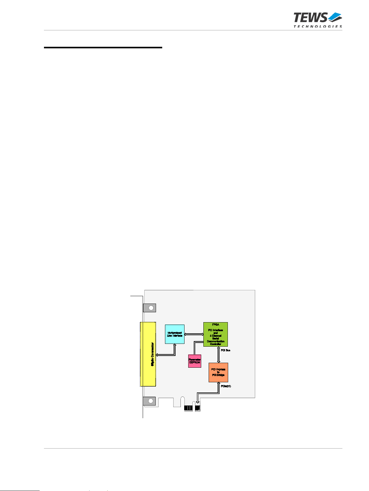
1 Product Description
The TPCE863 is a stand ar d he ight , ha lf leng th P CI Ex pr es s 1.1 compliant module with f our h igh sp eed s erial
data communication channels.
The serial communication controller is implemented in FPGA logic , along with the bus master capable PC I
interface, guarante eing long term availabi lity and having the opt ion to implement add itional functions in th e
future. The FPGA is connected to the PCI Express interface via a transparent PCI Express to PCI bridge.
Each channel provides a 5 12 DWORD (32 bit) r eceive FIFO and a transm it FIFO of up to 512 DW ORD (32
bit) for high data throughput.
Data transfer on the PCI Express bus is hand led v ia TPCE863 initiated DMA cycles with m inim um hos t/CPU
intervention.
Several serial comm unic ati on protoc o ls are s upported by each channel, such as as ynchron ous , is ochr on ous ,
synchronous and HDLC mode.
A 14.7456 MHz oscillator provides standard asynchronous b aud rates. A 24 MHz and a 10 MHz oscil lator
are provided for other (synchronous) baud rates.
Additionally each channe l provides various interrupt sources, generat ed on INT A. The interrupt sources can
be enabled or disabled individually.
Multiprotocol transce ivers are used for the line interface. The p hysical interface is selectable b y software,
individually for each channel as EIA-232, EIA-422, EIA 449, EIA-530, EIA-530A, V.35, V.36 or X.21.
A HD68 SCSI-3 type connector at the front panel provides access to the I/O lines.
The following signals are provided by the TPCE863 for each channel:
Receive Data (RxD +/-), Transmit Data (T x D +/-) , Rec ei ve C lock (RxC +/-), Tr ansmit Clock (TxC +/-), Ready-
To-Send (RTS +/-), Clear-To-Send (C T S +/-), Carrier-Detect (CD +/-) and GN D. Addition all y serial ch annel 3
provides Data-Set-Ready (DSR3 +/-) and Data-Terminal-Ready (DTR3 +/-).
A serial EEPROM is used to store detailed board information and special configuration parameters.
Operating temperature range is -40°C to +85°C.
Figure 1-1 : Block Diagram
TPCE863 User Manual Issue 1.0.1 Page 10 of 72
Page 11

2 Technical Specification
Interface
On Board Devices
PCI Express / PCI Bridge
Mechanical Interface
Electrical Interface
Serial Communication
Controller (FPGA)
I/O Interface
Number of Channels
Line Transceiver
FIFO
Data Rates
I/O Connector
Physical Data
PCISIG conforming PCI Express Revision 1.1
Standard Height, Half Length
PCISIG conforming PCI Express Revision 1.1
Single Link Width (x1)
PI7C9X111SL (Pericom Semiconductor Corporation)
XC3S1500-4FG(G)320I
Spartan-3 FPGA (Xilinx)
4
LTC2844/LTC2846 (Linear Technology) Multi-Protocol chip set,
software selectable, on-chip cable termination (LTC2846)
Main Transmit-FIFO per channel: up to 512 DWORD (2 Kbyte)
Main Receive-FIFO per channel: 512 DWORD (2 Kbyte)
SCC Transmit-FIFO per channel: up to 16 Byte
SCC Receive-FIFO per channel: 16 Byte
Synchronous: 10 Mbit/s (Non-DPLL Modes), 2 Mbit/s (DPLL
Modes)
Asynchronous: 2 Mbit/s
Front panel HD68 SCSI-3 Type Connector
(AMP 787082-7 or compatible)
Power Requirements
Temperature Range
MTBF
Humidity
Weight
51mA typical (no cable mode) @ +3.3V DC
81mA typical (V.28) @ +3.3V DC
1.15A typical (RS530/A) @ +3.3V DC
Operating
Storage
TPCE863-10R: 280988 h
MTBF values shown are based on calculation according to MIL-HDBK-217F and
MIL-HDBK-217F Notice 2; Environment: GB 20°C.
The MTBF calculation is based on component FIT rates provided by the
component suppliers. If FIT rates are not available, MIL-HDBK-217F and
MIL-HDBK-217F Notice 2 formulas are used for FIT rate calculation.
5 – 95 % non-condensing
TPCE863-10R: 86 g
Table 2-1 : Technical Specification
-40°C to +85°C
-40°C to +85°C
TPCE863 User Manual Issue 1.0.1 Page 11 of 72
Page 12

3 Handling and Operation Instructions
ESD Protection 3.1
The TPCE863 is sensitive to Electrostatic Discharge (ESD).
Packing, unpacking and all other handling of the TPCE863 has to be done
in an ESD/EOS protected Area.
TPCE863 User Manual Issue 1.0.1 Page 12 of 72
Page 13

4 On Board Devices
Overview 4.1
The DMA capable ser ial comm unication contro ller is im plemented in an on bo ard FPGA with i ntegrated PC I
bus interface (32 bit 33 MHz PCI bus).
The FPGA implements the serial communication controller logic and a register space and is the only
accessible device on the embedded TPCE863 PCI bus (except the PCIe/PCI bridge).
The PI7C9X111SL (Pericom Semiconductor Corporation) PCIe/PCI bridge is used as the bridging device
between the host PCIe interface and the on board PCI bus (i.e. the FPGA).
PI7C9X111SL PCIe/PCI Bridge 4.2
The PI7C9X111SL is a PCI Express to PCI reversible bridge. On the T PCE863 th e PI7C9X111SL is used in
transparent, forward mode only.
4.2.1 PI7C9X111SL Register Map
Register Group PCI Space
Configuration
Registers
Internal Configuration
Registers
PCI Compatible
Extended Capability
Registers for PCI
Express Interface
PCI Express
Extended Capability
Registers
PCI-Compatible Configuration Registers 0x00 – 0x3C
– 0x40 – 0x7C
PCI-Compatible Extende d C apa bi lity Registers 0x80 – 0xFF
PCI Express Extended Capability Registers 0x100 – 0xFFF
Table 4-1 : PI7C9X111SL Register Map
Offset Address
Range
TPCE863 User Manual Issue 1.0.1 Page 13 of 72
Page 14
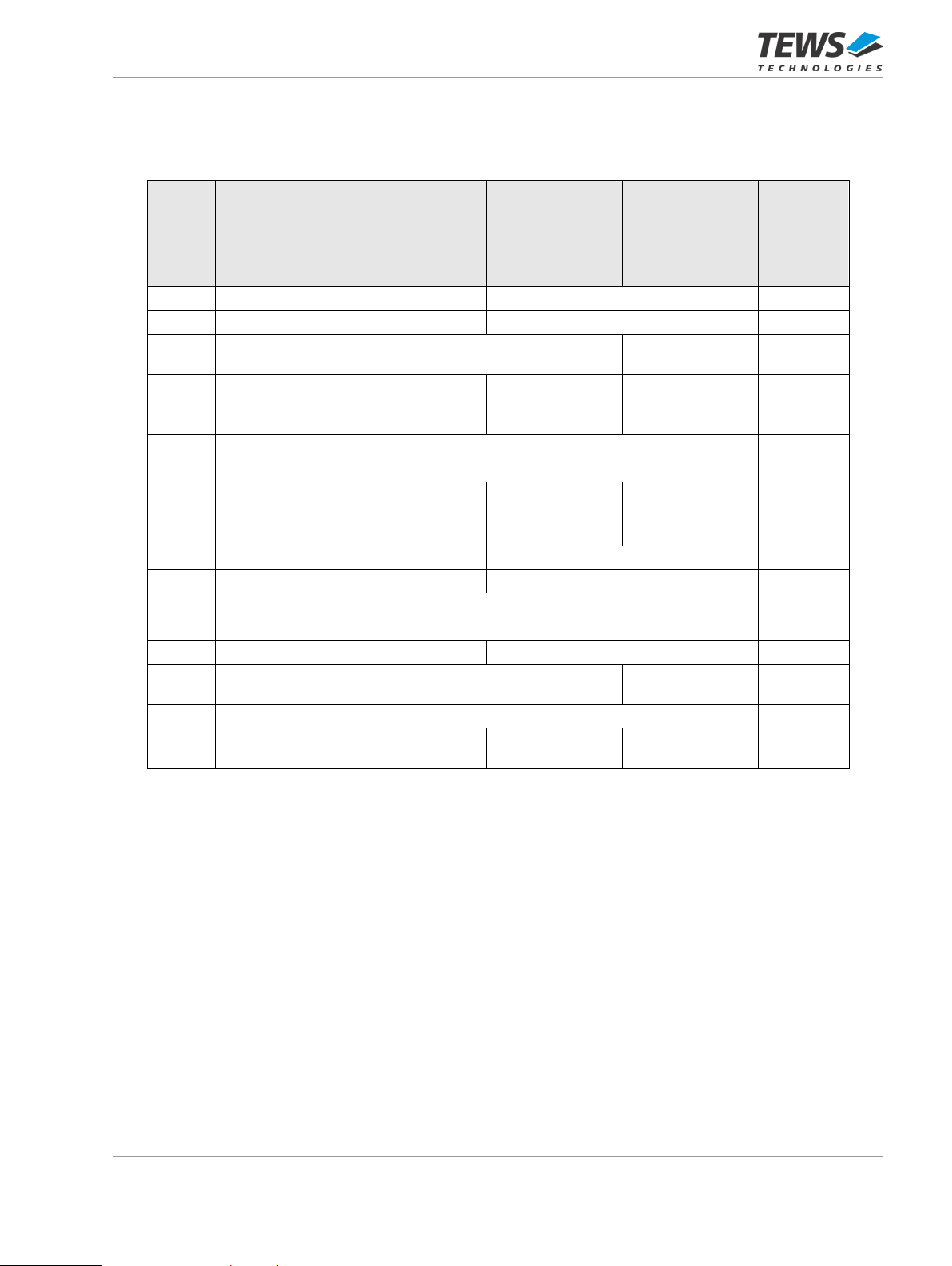
4.2.2 PCI Express Configurati on S pa ce Regis t e r Ma pping
4.2.2.1 PCI-Compatible Configuration (Type 1) Registers
PCI
CFG
Regist
er
Addres
s
0x00 PCI Device ID PCI Vendor ID E111 12D8
0x04 PCI Status PCI Command 0010 0000
0x08 PCI Class Code PCI Device
0x0C PCI Built-In Self-
0x10 PCI Base Address 0 00000000
0x14 PCI Base Address 1 00000000
0x18 Secondary
0x1C Secondary Status I/O Limit I/O Base 0200 01 01
0x20 Memory Limit Memory Base 0000 8000
0x24 Prefetchable Memory Limit Prefetchable Memory Base 0001 8001
0x28 Prefetchable Memory Base Upper 32 Bits 00000000
0x2C Prefetchable Memory Limit Upper 32 Bits 00000000
0x30 I/O Limit Upper 16 Bits I/O Base Upper 16 Bits 0000 0000
0x34 Reserved PCI Capabilities
0x38 PCI Base Address for Expansion ROM 00000000
0x3C Bridge Control Internal PCI
31 24 23 16 15 8 7 0 Read after
initializati
on write
access
060400 02
Revision ID
Test
(Not Supported)
Latency Timer
PCI Header Type Internal PCI Bus
Latency Timer
Subordinate Bus
Number
Secondary Bus
Number
Interrupt Wire
PCI Cache Line
Size
Primary Bus
Number
Pointer
Internal PCI
Interrupt Line
00 01 00
00
00 00 00
00
000000 80
0000 01 00
Table 4-2 : PI7C9X111SL PCI-Compatible Configuration (Type 1) Registers
TPCE863 User Manual Issue 1.0.1 Page 14 of 72
Page 15
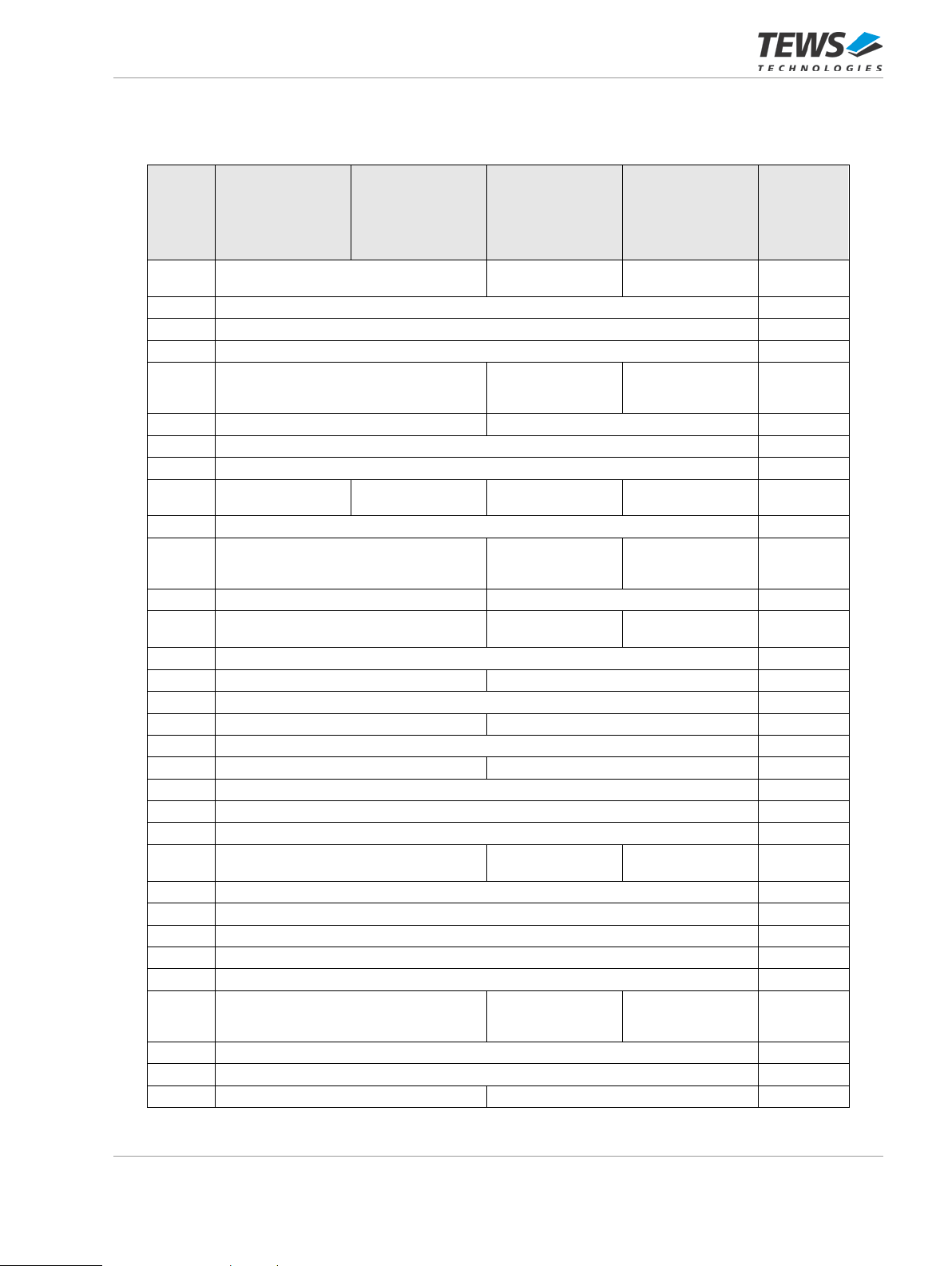
4.2.2.2 PCI-Compatible Extended Capability Registers
PCI
CFG
Registe
r
Addres
s
0x80 PCI-X Secondary Status
0x84 PCI-X Bridge Status Register 0000FFF8
0x88 Upstream Split Transaction 00100010
0x8C Downstream Split Transaction 00100010
0x90 Power Management Capabilities
0x94 PCI to PCI Support Extension Power Management Control/Status 0000 0000
0x98 Reserved 0x9C Reserved 0xA0 Chassis Number Slot Number
0xA4 Secondary Clock and ClkRun Control 0001 0000
0xA8 Reserved
0xAc Subsystem ID Subsystem Vendor ID 0000 0000
0xB0 PCI Express Capabilities
0xB4 Device Capabilities 0000 0022
0xB8 PCI Express Device Status PCI Express Device Control 0010 2000
0xBC Link Capabilities 00xx 3C11
0xC0 Link Status Link Control 1011 0000
0xC4 Slot Capabilit i es 0000 0000
0xC8 Slot Status Slot Control 0000 0000
0xCC XPIP Configuration 0 0400 1060
0xD0 XPIP Configuration 1 0400 0271
0xD4 XPIP Configuration 2 0019 0256
0xD8 VPD
0xDC VPD Data 0000 0000
0xE0 Reserved 0xE4 Reserved 0xE8 Reserved -
0xEC Reserved -
0xF0 Message Signaled I nterrupts Control
0xF4 Message Signaled Interrupts Address 0000 0000
0xF8 Message Signaled Interrupts Upper Address 0000 0000
0xFC Reserved Message Signaled Interrupts Data 0000 0000
31 24 23 16 15 8 7 0
PCI-X Next
Capability Pointer
Power Management
Next Capability
Pointer
Slot Identification
Capability Pointer
Subsystem and
Subsystem Vendor
ID Capability Pointer
PCI Express Next
Capability Pointer
VPD Capability
Pointer
Message Signaled
Interrupts Next
Capability Pointer
PCI-X Capability ID 0000 9007
Power Management
Capability ID
Slot Identification
Capability ID
Subsystem and
Subsystem Vendor
ID Capability ID
PCI Express
Capability ID
VPD Capability ID 0000 F003
Message Signaled
Interrupts Capability
ID
Read after
initializatio
n write
access
C843 A801
0000 B004
0000 B00D
0071 D810
0000 00 05
Table 4-3 : PI7C9X111SL PCI-Compatible Extended Capability Registers
TPCE863 User Manual Issue 1.0.1 Page 15 of 72
Page 16

4.2.3 Configura t ion EEPROM
After PCIe res et, the PI7C9X111SL loads initial configurati on register data from an on board configuration
I2C EEPROM. The content is a complete s et of conf iguration param eters based on the def ault settin gs with
the subsequent modifications.
For detailed information please refer to the PI7C9X111SL manual and Errata information.
Modifications are:
• Enable Lane Polarity Inversion (disabled by default)
SCC FPGA 4.3
The Serial Communication Controller (SCC) FPGA resides on the on board 32 bit 33 MHz PCI bus and is the
only other PCI device on the embedded PCI bus (PCI device number 0).
The FPGA implements a set of control & status registers as a PCI target, accessible in the PCI memor y
space.
The FPGA also im plements a PCI DMA/M aster engine used f or the data transf ers to and from host/s ystem
memory.
The FPGA configures from a serial Flash after power-up.
TPCE863 User Manual Issue 1.0.1 Page 16 of 72
Page 17
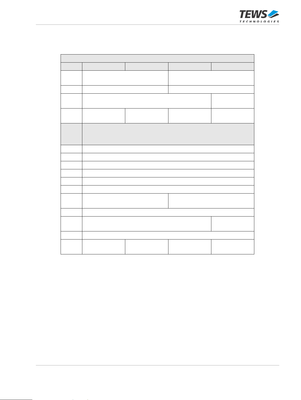
4.3.1 PCI Configuration Spac e
(SCC FPGA)
The SCC FPGA is assigned PCI device number 0 on the TPCE863 embedded PCI bus.
PCI Configuration Space Header
Offset 31 16 15 0
0x00
0x04 Status Command
0x08
0x0C BIST
0x10
0x14 Base Address Register 1 (not used)
0x18 Base Address Register 2 (not used)
0x1C Base Address Register 3 (not used)
0x20 Base Address Register 4 (not used)
0x24 Base Address Register 5 (not used)
0x28 CardBus CIS Pointer (not used)
0x2C
0x30 Expansion ROM Base Address (not used)
0x34 Reserved
0x38 Reserved
0x3C
Target register space of high speed serial communication controller
(TPCE863-10R: 0x700A)
Max_Lat
(0x0A)
Device ID
(TPCE863: 0x735F)
Class Code
(0x028000)
Header Type
(0x00)
Base Address Register 0
Subsystem ID
Min_Gnt
(0x03)
(TEWS Technologies 0x1498)
Lat. Timer Line Size
(TEWS Technologies 0x1498)
Int_Pin
(0x01)
Vendor ID
Rev ID
Subsystem Vendor ID
Cap. Pointer
(0x00)
Int_Line
Table 4-4 : PCI Configuration Space
TPCE863 User Manual Issue 1.0.1 Page 17 of 72
Page 18
5 Address Map
Space)
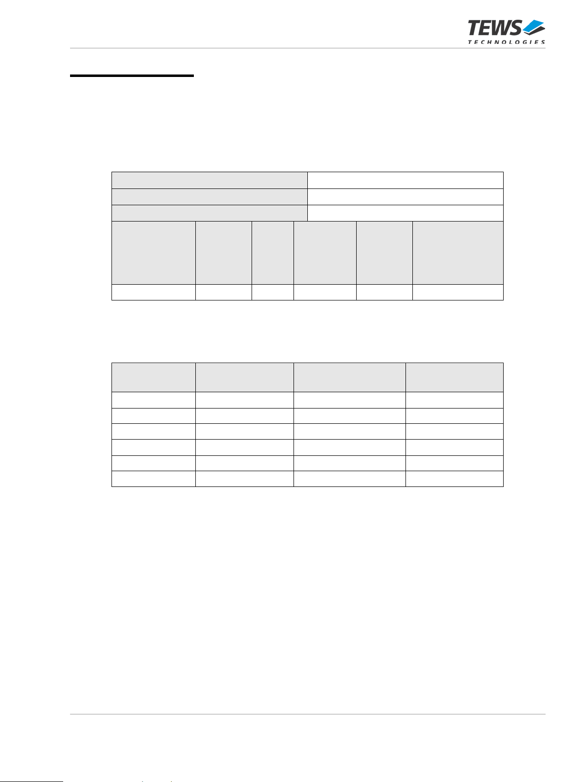
Register Space 5.1
The Register Space is accessible in the PCI Memory Space of the TPCE863 embedded PCI bus.
The Register Space Bas e addres s is f ound at PCI BA R0 (O ffs et 0x10) in th e PCI Conf igurat ion S pace of the
SCC FPGA (PCI device number 0 on the TPCE863 embedded PCI bus)
PCI Device Number
Device ID
Vendor ID
PCI Base
Address
(Offset in PCI
Configuration
0 (0x10) MEM 2048 32 Little Register Space
PCI Space
Mapping
Size
(Byte)
Table 5-1 : Register Space
0
0x735F (TPCE863)
0x1498 (TEWS Technologies)
Port Width
(Bit)
Endian
Mode
Description
Register Map 5.2
Offset to PCI
Base Address
0x0000 0x0000…0x00FF 44 (0x0000…0x00EC) Global Registers
0x0100 0x0100…0x017F 10 (0x0100…0x0158) SCC0 Registers
0x0180 0x0180…0x01FF 10 (0x0180…0x01D8) SCC1 Registers
0x0200 0x0200…0x027F 10 (0x0200…0x0258) SCC2 Registers
0x0280 0x0280…0x02FF 10 (0x0280…0x02D8) SCC3 Registers
0x0300 0x0300…0x07FF 0 (reserved)
Addresses range
Number of used
DWORD registers
Description
Table 5-2 : Register Map
TPCE863 User Manual Issue 1.0.1 Page 18 of 72
Page 19
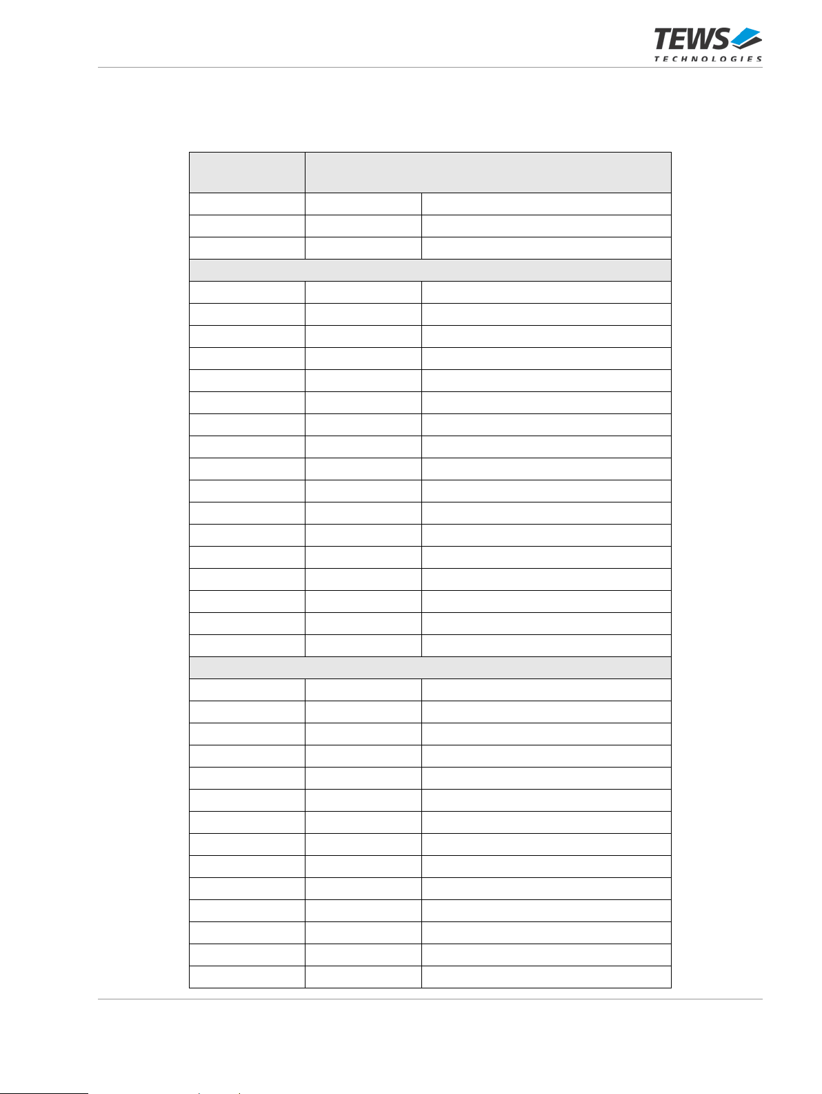
Global Register Map 5.3
All registers are 32 bit organized.
Offset to PCI
Base Address
0x0000 GCMDR Global Command Register
0x0004 GSTAR Global Status Register
0x0008 GMODE Global Mode Register
Interrupt Queue IQ specific registers (+ FIFO Control registers):
0x000C IQLENR0 IQ Length Register 0
0x0010 IQLENR1 IQ Length Register 1
0x0014 IQSCC0RXBAR IQ SCC0 RX Base Address Register
0x0018 IQSCC1RXBAR IQ SCC1 RX Base Address Register
0x001C IQSCC2RXBAR IQ SCC2 RX Base Address Register
0x0020 IQSCC3RXBAR IQ SCC3 RX Base Address Register
0x0024 IQSCC0TXBAR IQ SCC0 TX Base Address Register
0x0028 IQSCC1TXBAR IQ SCC1 TX Base Address Register
0x002C IQSCC2TXBAR IQ SCC2 TX Base Address Register
0x0030 IQSCC3TXBAR IQ SCC3 TX Base Address Register
0x0034 FIFOCR4 FIFO Control Register 4
0x0038 reserved -
0x003C IQCFGBAR IQ CFG Base Address Register
0x0040 reserved 0x0044 FIFOCR1 FIFO Control Register 1
0x0048 reserved -
0x004C reserved -
DMA Controller (DMAC) specific registers:
0x0050 CH0CFG Channel 0 Configuration Register
0x0054 CH0BRDA Channel 0 Base Rx Descr. Address
0x0058 CH0BTDA Channel 0 Base Tx Descr. Address
0x005C CH1CFG Channel 1 Configuration Register
0x0060 CH1BRDA Channel 1 Base Rx Descr. Address
0x0064 CH1BTDA Channel 1 Base Tx Descr. Address
0x0068 CH2CFG Channel 2 Configuration Register
0x006C CH2BRDA Channel 2 Base Rx Descr. Address
0x0070 CH2BTDA Channel 2 Base Tx Descr. Address
0x0074 CH3CFG Channel 3 Configuration Register
0x0078 CH3BRDA Channel 3 Base Rx Descr. Address
0x007C CH3BTDA Channel 3 Base Tx Descr. Address
0x0080...0x0097 reserved -
0x0098 CH0FRDA Channel 0 First Rx Descr. Address
Register Name
TPCE863 User Manual Issue 1.0.1 Page 19 of 72
Page 20

Offset to PCI
Base Address
0x009C CH1FRDA Channel 1 First Rx Descr. Address
0x00A0 CH2FRDA Channel 2 First Rx Descr. Address
0x00A4 CH3FRDA Channel 3 First Rx Descr. Address
0x00A8 reserved 0x00AC reserved 0x00B0 CH0FTDA Channel 0 First Tx Descr. Address
0x00B4 CH1FTDA Channel 1 First Tx Descr. Address
0x00B8 CH2FTDA Channel 2 First Tx Descr. Address
0x00BC CH3FTDA Channel 3 First Tx Descr. Address
0x00C0 reserved 0x00C4 reserved 0x00C8 CH0LRDA Channel 0 Last Rx Descr. Address
0x00CC CH1LRDA Channel 1 Last Rx Descr. Address
0x00D0 CH2LRDA Channel 2 Last Rx Descr. Address
0x00D4 CH3LRDA Channel 3 Last Rx Descr. Address
0x00D8 reserved -
0x00DC reserved -
0x00E0 CH0LTDA Channel 0 Last Tx Descr. Address
0x00E4 CH1LTDA Channel 1 Last Tx Descr. Address
0x00E8 CH2LTDA Channel 2 Last Tx Descr. Address
0x00EC CH3LTDA Channel 3 Last Tx Descr. Address
Other registers:
0x00F0 VR Version Register
0x00F4 ISPR ISP Register
0x00F8 GCTLR Global Control Register
0x00FC...0x00FF reserved -
Register Name
Table 5-3 : Global Register Map
SCC Register Map 5.4
The SCC registers are used to configure and control each of the four integrated Serial Communication
Controller (SCC).
There is one complete SCC register set for each of the four SCC channels (0 … 3).
The address of a certain SCC register is:
Register Space PCI Base Address + SCC Channel Offset + SCC Register Offset
Register Space PCI Base Address:
PCI Base Address 0
(Offset 0x10 in the PCI Configuration Space of the FPGA PCI Device)
TPCE863 User Manual Issue 1.0.1 Page 20 of 72
Page 21
SCC Channel Offset:
SCC0 (Channel 0): 0x0100
SCC1 (Channel 1): 0x0180
SCC2 (Channel 2): 0x0200
SCC3 (Channel 3): 0x0280
SCC Register Offset:
Register address offset, range 0x00 … 0x5C (see SCC Register Map table)
Most registers and reg ister bit positions are sh ared by all SCC protocol m odes (HDLC, ASYNC). H owever
the meaning (and nam e) of single b it positions might differ bet ween different protocol m odes. All registers
are 32-bit organized registers.
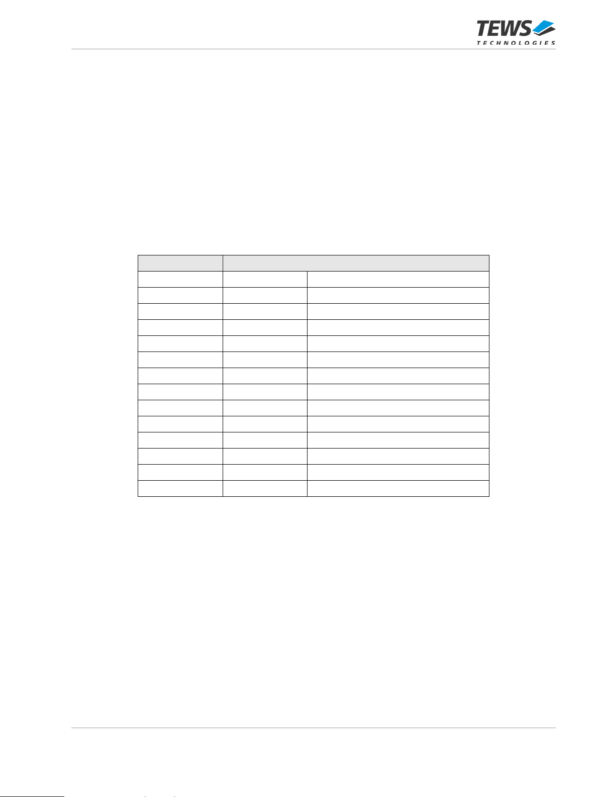
Each SCC channel register set contains the following registers:
Register Offset Register Name
0x00 CMDR Command Register
0x04 STAR Status Register
0x08 CCR0 Channel Configuration Register 0
0x0C CCR1 Channel Configuration Register 1
0x10 CCR2 Channel Configuration Register 2
0x14…0x2B reserved -
0x2C BRR Baud Rate Register
0x30…0x47 reserved -
0x48 TCR Termination Character Register
0x4C…0x53 reserved -
0x54 IMR Interrupt Mask Register
0x58 ISR Interrupt Status Register
0x5C ACR Additional Configuration Register
0x60...0x7F reserved -
Table 5-4 : SCC Register Map
TPCE863 User Manual Issue 1.0.1 Page 21 of 72
Page 22
Global Registers 5.5
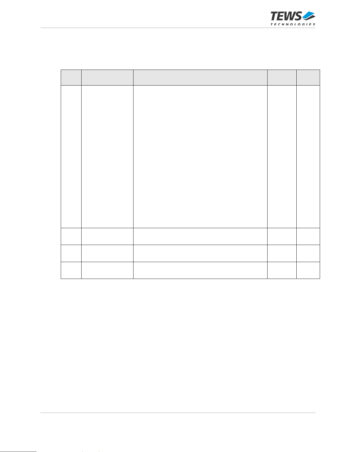
5.5.1 GCMDR – Global Command Register (0x0000)
Bit Symbol Description Access Reset
31 CFGIQSCC3RX Configure Interrupt Queue SCC3 Receive
Only valid, if action request bit ’AR’ is set.
The DMA (interrupt) controller will transfer
interrupt vectors generated by the dedicated SCC
receiver (3..0) to the corresponding interrupt
queue which must be configured via
’CFGIQSCCiRX’ command bits:
’0’: The DMA (interrupt) controller does NOT
configure/re-configure the corresponding
interrupt queue, if action request bit ’AR’ is
set to ’1’.
’1’: Causes the DMA (interrupt) controller to
configure/re-configure the corresponding
interrupt queue, if action request bit ’AR’ is
set to ’1’.
Upon action request, the DMA (interrupt)
controller will evaluate the corresponding
interrupt queue base address and length
registers which must have been programmed
by software before.
30 CFGIQSCC2RX Configure Interrupt Queue SCC2 Receive
(see above)
29 CFGIQSCC1RX Configure Interrupt Queue SCC1 Receive
(see above)
28 CFGIQSCC0RX Configure Interrupt Queue SCC0 Receive
(see above)
Value
R/W 0
R/W 0
R/W 0
R/W 0
TPCE863 User Manual Issue 1.0.1 Page 22 of 72
Page 23

Bit Symbol Description Access Reset
Value
27 CFGIQSCC3TX Configure Interrupt Queue SCC3 Transmit
Only valid, if action request bit ’AR’ is set.
The DMA (interrupt) controller will transfer
interrupt vectors generated by the dedicated SCC
transmitter (3..0) to the corresponding interrupt
queue which must be configured via
’CFGIQSCCiTX’ command bits:
’0’: The DMA (interrupt) controller does NOT
configure/re-configure the corresponding
interrupt queue, if action request bit ’AR’ is
set to ’1’.
’1’: Causes the DMA (interrupt) controller to
configure the corresponding interrupt queue,
if action request bit ’AR’ is set to ’1’.
Upon action request, the DMA (interrupt)
controller will evaluate the corresponding
interrupt queue base address and length
registers which must have been programmed
by software before.
26 CFGIQSCC2TX Configure Interrupt Queue SCC2 Transmit
(see above)
25 CFGIQSCC1TX Configure Interrupt Queue SCC1 Transmit
(see above)
24 CFGIQSCC0TX Configure Interrupt Queue SCC0 Transmit
(see above)
23:22 - Reserved (0 for reads) R 0
21 CFGIQCFG Configure Interrupt Queue Configuration
Only valid, if action request bit ’AR’ is set.
The DMA (interrupt) controller will transfer action
request acknowledge/failure interrupt vectors to
the configuration interrupt queue which must be
configured via ’CFGIQCFG’ command bits:
R/W 0
R/W 0
R/W 0
R/W 0
R/W 0
’0’: The DMA (interrupt) controller does NOT
configure/re-configure the configuration
interrupt queue, if action request bit ’AR’ is
set to ’1’.
’1’: Causes the DMA (interrupt) controller to
configure the configuration interrupt queue, if
action request bit ’AR’ is set to ’1’.
Upon action request, the DMA (interrupt)
controller will evaluate the configuration
interrupt queue base address and length
registers which must have been programmed
by software before.
20:14 - Reserved (0 for reads) R 0
TPCE863 User Manual Issue 1.0.1 Page 23 of 72
Page 24

Bit Symbol Description Access Reset
Value
13 TXPR3 Transmit Poll Request Channel 3
Self-clearing command bit, only valid in ’HOLD’ bit
controlled DMA controller mode (bit CMODE = ’0’
in register GMODE):
’0’: No Transmit Poll Request is performed. The
corresponding DMA controller transmit
channel is stopped when HOLD=’1’ has been
detected in the current transmit descriptor.
’1’: Setting this bit to ’1’, when HOLD=’1’ has
been detected in the current transmit
descriptor, will cause the controller to poll the
’HOLD’ bit in the current transmit descriptor,
i.e. the controller reads the configuration word
(DWORD 0) and next descriptor address
(DWORD 1) of the current descriptor again. If
the ’HOLD’ bit is detected cleared (’0’), the
DMA controller will branch to the next
descriptor.
When the DMA controller is not in ’HOLD’
state, this command is discarded.
12 TXPR2 Transmit Poll Request Channel 2 R/W 0
11 TXPR1 Transmit Poll Request Channel 1 R/W 0
10 TXPR0 Transmit Poll Request Channel 0 R/W 0
9 IMAR Interrupt Mask Action Request R/W 1
8:1 - Reserved (0 for reads) R 0
0 AR Action Request
Self-clearing command bit.
'0': No action request
'1': Action request
Validates GCMDR CFGIQSCCiRX,
CFGIQSCCiTX, CFGIQCFG register bits and
CHiCFG RDR, RDT, IDR, IDT register bits.
R/W 0
R/W 0
Table 5-5 : Global Command Register
TPCE863 User Manual Issue 1.0.1 Page 24 of 72
Page 25

5.5.2 GSTAR – Global Status Register (0x0004)
Status set by DMA Controller as an interrupt indication
The Global Status Register indicates whether an action request was executed successfully or not. It also
gives information about th e interrupt source and which interr upt queue has been written to when I NTA# is
activated.
Nine interrupt queues are provided:
– four receive interrupt vector queues (one for each SCCi, i=0...3)
– four transmit interrupt vector queues (one for each SCCi, i=0...3)
– one configuration interrupt vector queue (action request acknowledge/fail)
To clear a bit in the status register, the host CPU must write a ‘1’ to the corresponding register bit.
The PCI interrupt signa l INT A# will be asserted if any of the GSTAR interr upt indic ations bits is s et. The PCI
interrupt signal INTA# will be de-asserted if all GSTAR Interrupt Indication bits are c leared.
Bit Symbol Description Access Reset
Value
31 IISCC3RX Interrupt Indication Queue SCC3 Receive R/C 0
30 IISCC2RX Interrupt Indication Queue SCC2 Receive R/C 0
29 IISCC1RX Interrupt Indication Queue SCC1 Receive R/C 0
28 IISCC0RX Interrupt Indication Queue SCC0 Receive
These bits indicate whether at least one new
interrupt vector was transferred into the
corresponding receive interrupt queue:
R/C 0
’0’: No new interrupt vector was transferred into
the corresponding queue.
’1’: At least one new interrupt vector was
transferred into the corresponding queue.
27 IISCC3TX Interrupt Indication Queue SCC3 Transmit R/C 0
26 IISCC2TX Interrupt Indication Queue SCC2 Transmit R/C 0
25 IISCC1TX Interrupt Indication Queue SCC1 Transmit R/C 0
24 IISCC0TX Interrupt Indication Queue SCC0 Transmit
These bits indicate whether at least one new
interrupt vector was transferred into the
corresponding transmit interrupt queue:
’0’: No new interrupt vector was transferred into
the corresponding queue.
’1’: At least one new interrupt vect or was
transferred into the corresponding queue.
23:22 - Reserved (0 for reads) R 0
R/C 0
TPCE863 User Manual Issue 1.0.1 Page 25 of 72
Page 26

Bit Symbol Description Access Reset
Value
Value
21 IICFG Interrupt Indication Configuration Queue
These bits indicate whether at least one new
interrupt vector was transferred into the
configuration interrupt que u e:
’0’: No new interrupt vector was transferred into
the corresponding queue.
’1’: At least one new interrupt vect or was
transferred into the corresponding queue.
20:2 - Reserved (0 for reads) R 0
Action Request Result Status
1 ARF Action Request Failed Status
This bit indicates that an action request command
was completed with an ’action request failed’
condition:
’0’: No action request was performed or no
’action request failed’ condition occurred
completing an action request.
’1’: The last action request command was
completed with an ’action request failed’
condition.
0 ARACK Action Request Acknowledge Status
This bit indicates that an action request command
was completed successfully:
R/C 0
R/C 0
R/C 0
’0’: No action request was performed or
completed successfully.
’1’: The last action request command was
completed successfully.
Table 5-6 : Global Status Register
5.5.3 GMODE – Gl obal Mode Re gister (0x0008)
Bit Symbol Description Access Reset
31:1 - Reserved (0 for reads) R 0
0 CMODE DMA Control Mode
’0’ ’ HOLD’ bit control mode. The descriptor chain
end condition is controlled via the ’HOLD’ bit
in each receive/transmit descriptor.
’1’ Last Receive/Transmit Descriptor Address
mode. The descriptor chain end condition is
controlled via registers LRDA/LTDA.
Table 5-7 : Global Mode Register
R/W 0
TPCE863 User Manual Issue 1.0.1 Page 26 of 72
Page 27
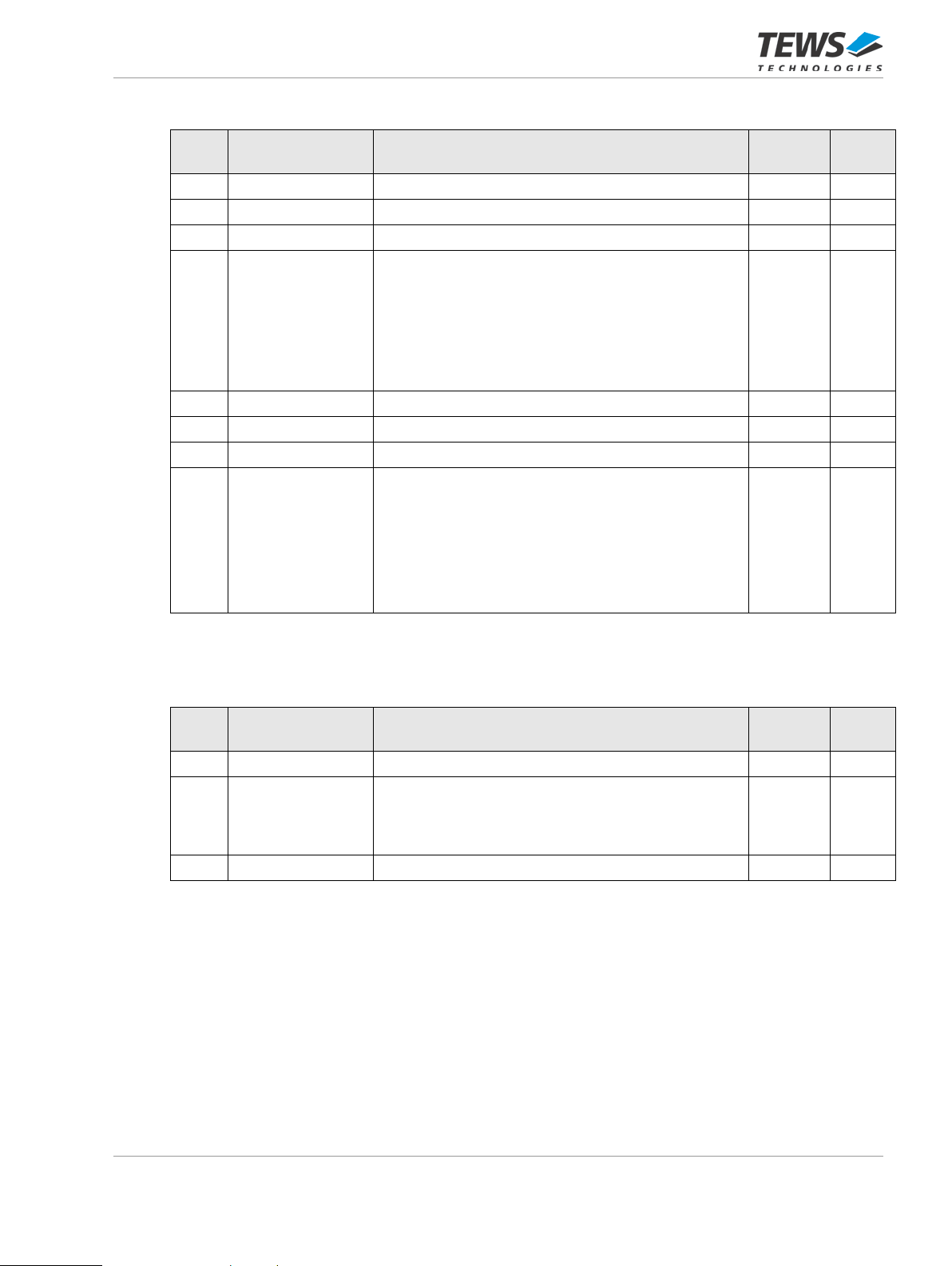
5.5.4 IQLENR0 – Interrupt Queue Le ngt h Regis t e r 0 (0x000C)
31:24
-
Reserved (0 for reads)
R
0
Bit Symbol Description Access Reset
31:28 IQSCC0RXLEN Interrupt Queue SCC3 Receive Length R/W 0
27:24 IQSCC1RXLEN Interrupt Queue SCC2 Receive Length R/W 0
23:20 IQSCC2RXLEN Interrupt Queue SCC1 Receive Length R/W 0
19:16 IQSCC3RXLEN Interrupt Queue SCC0 Receive Length
These bit fields determine the length of the
corresponding receive interrupt queue (related to
the respective SCC receive channel):
Queue Length = (1 + ’IQSCCiRXLEN’) * 32 DWORDS
’IQSCCiRXLEN’ = 0...15
15:12 IQSCC0TXLEN Interrupt Queue SCC3 Transmit Length R/W 0
11:8 IQSCC1TXLEN Interrupt Queue SCC2 Transmit Length R/W 0
7:4 IQSCC2TXLEN Interrupt Queue SCC1 Transmit Length R/W 0
3:0 IQSCC3TXLEN Interrupt Queue SCC0 Transmit Length
These bit fields determine the length of the
corresponding transmit interrupt queue (related to
the respective SCC transmit channel):
Queue Length = (1 + ’IQSCCiTXLEN’) * 32 DWORDS,
’IQSCCiTXLEN’ = 0...15
Value
R/W 0
R/W 0
Table 5-8 : Interrupt Queue Length Register 0
5.5.5 IQLENR1 – Interrupt Queue Length Register 1 (0x0010)
Bit Symbol Description Access Reset
23:20 IQCFGLEN Interrupt Queue Configuration Length
Queue Length = (1 + ’IQCFGLEN’) * 32 DWORDS,
’IQCFGLEN’ = 0...15
19:0 - Reserved (0 for reads) R 0
Table 5-9 : Interrupt Queue Length Register 1
Value
R/W 0
TPCE863 User Manual Issue 1.0.1 Page 27 of 72
Page 28
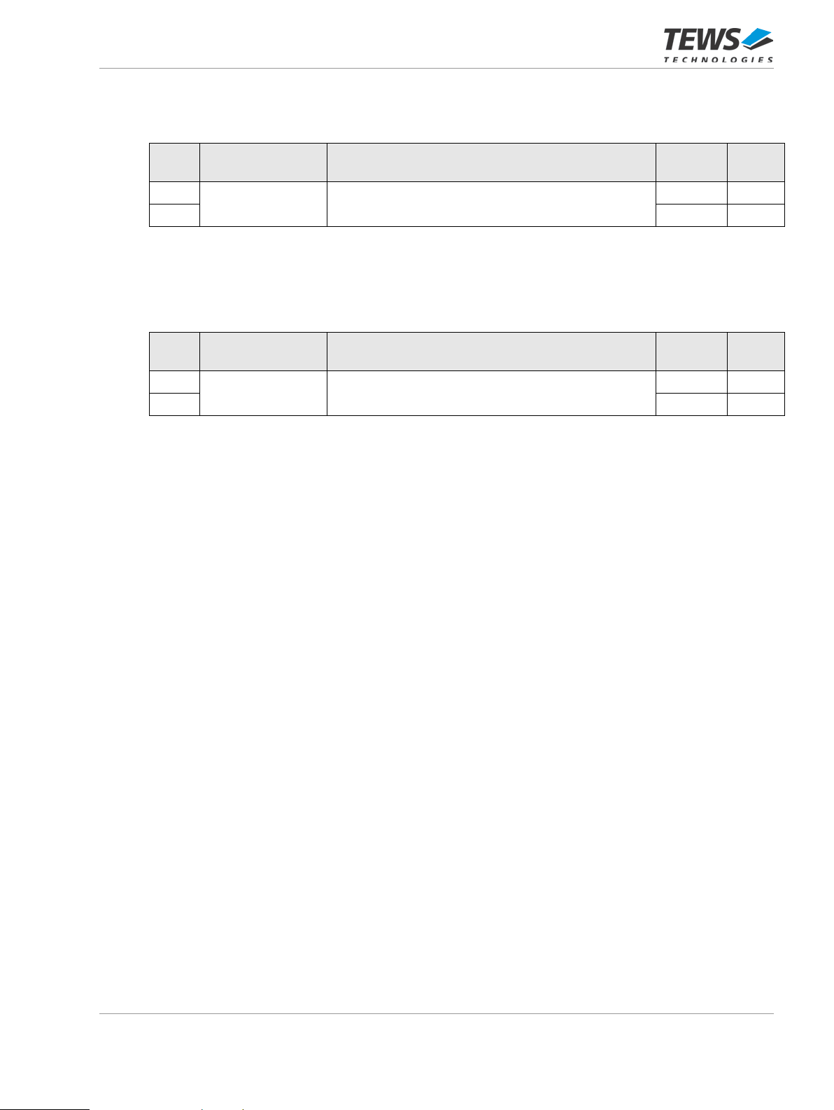
5.5.6 IQSCCiRXBAR – Interr upt Queue SCCi Re c e iver Base Address Register (i=0...3) (0x0014, 0x0018, 0x001C, 0x0020)
Bit Symbol Description Access Reset
Value
31:2 IQSCCiRXBAR PCI Base Address of Receive Interrupt Queue R/W 0
1:0 R 0
Table 5-10: IQSCCiRXBAR Register
5.5.7 IQSCCiTXBAR – Interrupt Queue SCCi Transmitter Base Address Register (i=0...3) (0x0024, 0x0028, 0x002C, 0x0030)
Bit Symbol Description Access Reset
Value
31:2 IQSCCiTXBAR PCI Base Address of Transmit Interrupt Queue R/W 0
1:0 R 0
Table 5-11: IQSCCiTXBAR Register
TPCE863 User Manual Issue 1.0.1 Page 28 of 72
Page 29

5.5.8 FIFOCR4 – FIFO Control Regi ster 4 (0x0034)
Bit Symbol Description Access Reset
31:24 TFFTHRES3 Transmit FIFO Forward Threshold Channel 3 R/W 0
23:16 TFFTHRES2 Transmit FIFO Forward Threshold Channel 2 R/W 0
15:8 TFFTHRES1 Transmit FIFO Forward Threshold Channel 1 R/W 0
:0 TFFTHRES0 Transmit FIFO Forward Threshold Channel 0
These bit fields determine the channel specific
Transmit FIFO Forward Threshold for the
corresponding channel i in number of DWORDs.
This threshold controls DMAC operation towards
the serial channels (SCCi).
As soon as the number of valid data words
(belonging to a frame) in the main transmit FIFO is
greater than the threshold, the DMAC will provide
transmit data to the corresponding SCC. Once
having started serving data for a frame, the DMAC
will ignore this threshold providing all available
data of the current frame to the SCC. Threshold
operation starts again with the next frame. Frames
shorter than the threshold will be transferred as
soon as a frame end indication is detected by the
DMAC.
Note: Programming TFFTHRESi to zero will disable the
threshold causing the DMAC to transfer all data
immediately. This may be useful for not frame
oriented data transmission, e.g. in ASYNC
protocol mode.
Value
R/W 0
Table 5-12 : FIFO Control Register 4
TPCE863 User Manual Issue 1.0.1 Page 29 of 72
Page 30
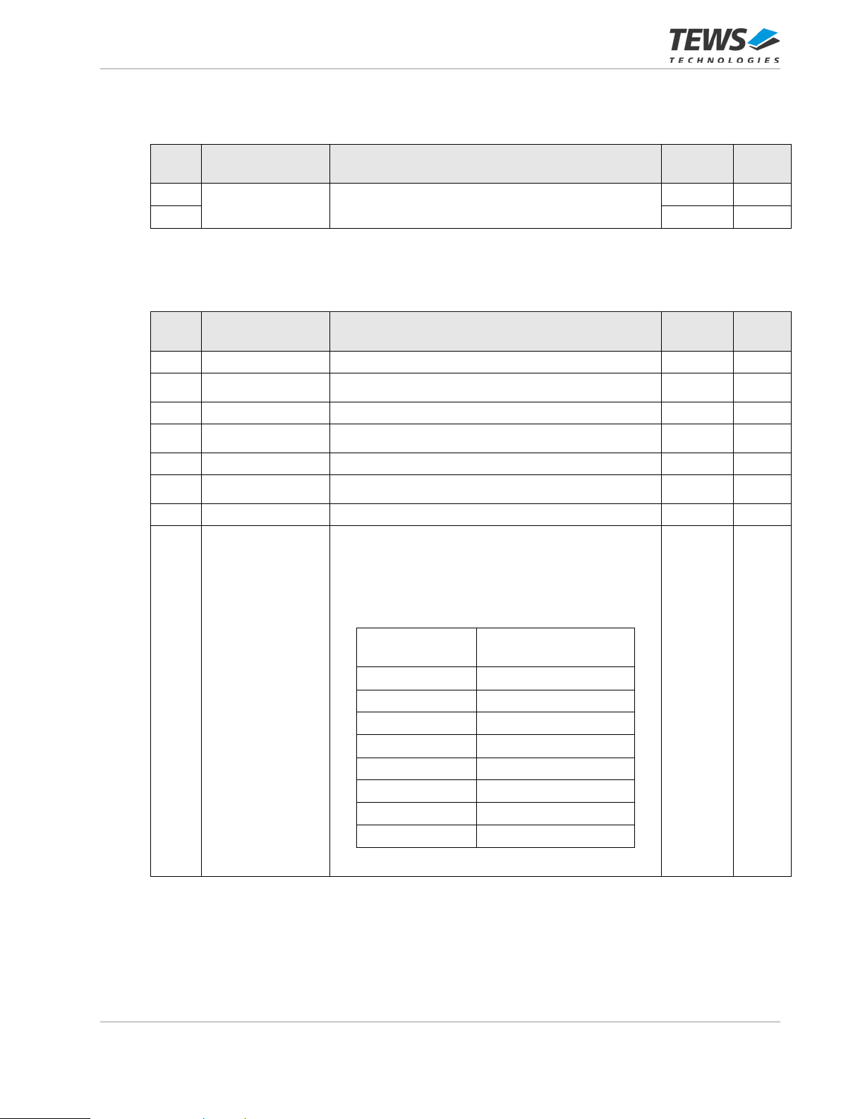
5.5.9 IQCFGBAR – Interrupt Que ue Conf iguration Base Address Register (0x003C)
Bit Symbol Description Access Reset
31:2 IQCFGBAR PCI Base Address of Configuration Interrupt
1:0 R 0
Queue
Table 5-13: IQCFGBAR Register
R/W 0
5.5.10 FIFOCR1 – FIFO Control Register 1 (0x0044)
Bit Symbol Description Access Reset
31:27 - Reserved (0 for reads) R 0
26:24 TFSIZE3
23:19 - Reserved (0 for reads) R 0
18:16 TFSIZE2
15:9 - Reserved (0 for reads) R 0
10:8 TFSIZE1
7:3 - Reserved (0 for reads) R 0
2:0 TFSIZE0
Main Transmit-FIFO Size (Depth) Channel 3
Main Transmit-FIFO Size (Depth) Channel 2
Main Transmit-FIFO Size (Depth) Channel 1
Main Transmit-FIFO Size (Depth) Channel 0
R/W 111
R/W 111
R/W 111
R/W 111
Value
Value
Main Transmit-FIFO Size (Depth) is
2 power (TFSIZEi + 2)
TFSIZEi
111 512
110 256
101 128
100 64
011 32
010 16
001 8
000 4
Table 5-14: FIFO Control Register 1
FIFO Size (Depth) in
DWords (4 Bytes)
TPCE863 User Manual Issue 1.0.1 Page 30 of 72
Page 31

5.5.11 CHiCFG – Channel i Configuration Regi ster (i=0...3) (0x0050, 0x005C, 0x0068, 0x0074)
Bit Symbol Description Access Reset
31:28 - Reserved (0 for reads) R 0
27 MRFI Mask Receive FI Interrupt (Channel i)
This bit enables/disables the receive FI interrupt
indication for the DMA channel, the register is
dedicated to (i=3..0):
’0’: FI interrupt generation is enabled for the
dedicated DMA receive channel.
’1’: FI interrupt generation is disabled for the
dedicated DMA receive channel.
26 MTFI Mask Transmit FI Interrupt (Channel i)
This bit enables/disables the transmit FI interrupt
indication for the DMA channel, the register is
dedicated to (i=3..0):
’0’: FI interrupt generation is enabled for the
dedicated DMA transmit channel.
Value
R/W 0
R/W 0
’1’: FI interrupt generation is disabled for the
dedicated DMA transmit channel.
25 MRERR Mask Receive ERR Interrupt (Channel i)
This bit enables/disables the receive ERR
interrupt indication for the DMA channel, the
register is dedicated to (i=3..0):
’0’: ERR interrupt generation is enabled for the
dedicated DMA receive channel.
’1’: ERR interrupt generation is disabled for the
dedicated DMA receive channel.
24 MTERR Mask Transmit ERR Interrupt (Channel i)
This bit enables/disables the transmit ERR
interrupt indication for the DMA channel, the
register is dedicated to (i=3..0):
’0’: ERR interrupt generation is enabled for the
dedicated DMA transmit channel.
’1’: ERR interrupt generation is disabled for the
dedicated DMA transmit channel.
23 - Reserved (0 for reads) R 0
R/W 0
R/W 0
TPCE863 User Manual Issue 1.0.1 Page 31 of 72
Page 32

Bit Symbol Description Access Reset
Value
22 RDR Reset DMA Receiver (Channel i)
R/W 0
Must be validated by the Action Request bit in the
GCMDR. Cleared automatically if successful.
This command resets the specific DMA controller
receive channel and also flushes the receive data
FIFO. After reset, the respective DMA channel is
in its initial state equal to the reset state after
power on. The receive data FIFO will not accept
any receive data until the IDR command is
successfully finished.
21 RDT Reset DMA Transmitter (Channel i)
R/W 0
Must be validated by the Action Request bit in the
GCMDR. Cleared automatically if successful.
This command resets the specific DMA controller
transmit channel. After reset, the respective DMA
channel is in its initial state equal to the reset state
after power on.
20 IDR Initialize DMA Receiver (Channel i)
R/W 0
Must be validated by the Action Request bit in the
GCMDR. Cleared automatically if successful.
This command causes the specific DMA receive
channel to fetch the base descriptor address from
register CHiBRDA and to branch to the
corresponding descriptor. Afterwards normal DMA
operation on the receive descriptor list is
performed depending on the selected DMA control
mode.
Note: To avoid unexpected DMA controller behavior, it
is recommended to apply ’IDR’ command only, if
the specific DMA channel is in reset state.
19 IDT Initialize DMA Transmitter (Channel i)
R/W 0
Must be validated by the Action Request bit in the
GCMDR. Cleared automatically if successful.
This command causes the specific DMA transmit
channel to fetch the base descriptor address from
register CHiBTDA and to branch to the
corresponding descriptor. Afterwards normal DMA
operation on the transmit descriptor list is
performed depending on the selected DMA control
mode.
Note: To avoid unexpected DMA controller behavior, it
is recommended to apply ’IDT’ command only, if
the specific DMA channel is in reset state.
18:0 - Reserved (0 for reads) R 0
Table 5-15: CHiCFG Register
TPCE863 User Manual Issue 1.0.1 Page 32 of 72
Page 33
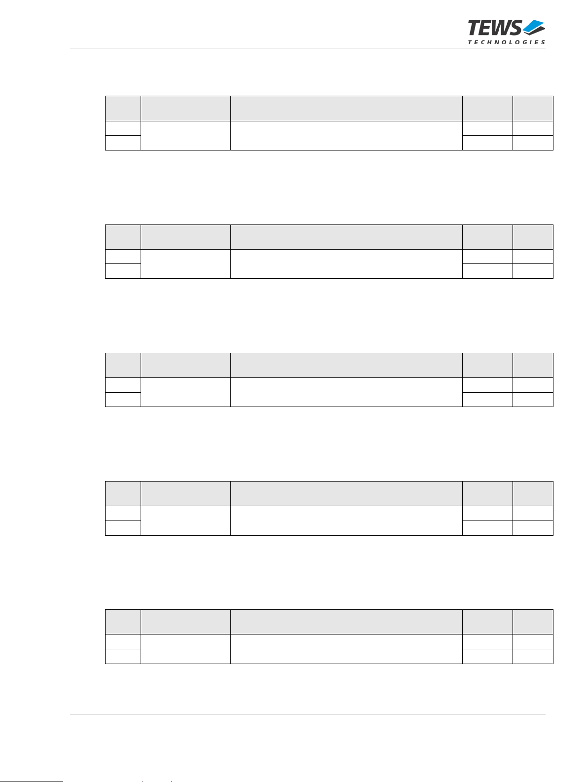
5.5.12 CHiBRDA – Channel i Base Receive Descriptor Address Register (i=0...3) (0x0054, 0x0060, 0x006C, 0x0078)
Bit Symbol Description Access Reset
Value
31:2 CHiBRDA PCI Base Address of Receive Descriptor R/W 0
1:0 R 0
Table 5-16: CHiBRDA Register
5.5.13 CHiBTDA – Channel i Base Transmit Descriptor Address Register (i=0...3) (0x0058, 0x0064, 0x0070, 0x007C)
Bit Symbol Description Access Reset
Value
31:2 CHiBTDA PCI Base Address of Transmit Descriptor R/W 0
1:0 R 0
Table 5-17: CHiBTDA Register
5.5.14 CHiFRDA – Channel i First (Curr e nt ) Receive Descriptor Address Register (i=0...3) (0x0098, 0x009C, 0x00A0, 0x00A4)
Bit Symbol Description Access Reset
Value
31:2 CHiFRDA DMAC enters the PCI Base Address of the current
1:0 R 0
Receive Descriptor
Table 5-18: CHiFRDA Register
R 0
5.5.15 CHiFTDA – Channel i First (Curr e nt ) Transmit Descriptor Address Register (i=0...3) ( 0x00B0, 0x00B4, 0x00B8, 0x00BC)
Bit Symbol Description Access Reset
Value
31:2 CHiFRDA DMAC enters the PCI Base Address of the current
1:0 R 0
Transmit Descriptor
Table 5-19: CHiFTDA Register
R 0
5.5.16 CHiLRDA – Channel i Last Receive Descriptor Address Register (i=0...3) (0x00C8, 0x00CC, 0x00D0, 0x00D4)
Bit Symbol Description Access Reset
Value
31:2 CHiLRDA PCI Base Address of Last Receive Descriptor R/W 0
1:0 R 0
Table 5-20: CHiLRDA Register
TPCE863 User Manual Issue 1.0.1 Page 33 of 72
Page 34
5.5.17 CHiLTDA – Channel i Last Transmit Descriptor Address Register (i=0...3) (0x00E0, 0x00E4, 0x00E8, 0x00EC)
Bit Symbol Description Access Reset
Value
31:2 CHiLTDA PCI Base Address of Last Transmit Descriptor R/W 0
1:0 R 0
Table 5-21: CHiLTDA Register
5.5.18 VR – Version Register (0x00F0)
Bit Symbol Description Access Reset
Value
31:16 SPC_ID Reserved (0 for reads) or special customer ID register R 0
15:0 VER FPGA Logic Version R 0x0007
Table 5-22: Version Register
5.5.19 ISPR – In-System-Programming Re gister (0x00F4)
This register is reserved for (factory) reprogramming of the FPGA configuration flash.
No write accesses shall be done to this address, as permanent damage may occur.
TPCE863 User Manual Issue 1.0.1 Page 34 of 72
Page 35
5.5.20 GCTLR – Global Control Register (0x00F8)
Bit Symbol Description Access Reset
31:20 - Reserved (0 for reads) R 0
19 EEDO Serial EEPROM Data Out (Q) R 18 EEDI Serial EEPROM Data In (D) R/W 0
17 EECS Serial EEPROM Chip Select (S) R/W 0
16 EESK Se rial EEPROM Clock (C) R/W 0
15:8 RETRYCNT Maximum number of retries, that occurred during a PCI
transaction
7 RCNTCLR Reset maximum number of retries
Self-clearing command bit
6 INI_HALT Initiator State Machine is stopped due to PCI transaction
abort
5 INI_REL Release the stopped Initiator State Machine
Self-clearing command bit
4:1 - Reserved R 0
0 LRST Local Reset
Self-clearing command bit.
The complete local part of the device is reset. Only the
registers in the PCI configuration space keep their values.
Value
R 0x00
R/W 0
R 0
R/W 0
R/W 0
Table 5-23: Global Control Register
TPCE863 User Manual Issue 1.0.1 Page 35 of 72
Page 36

SCC Channel Speci f ic Registers 5.6
5.6.1 CMDR – Command Register (0x0100, 0x0180, 0x0200, 0x0280)
Bit Symbol Description Access Reset
31:25 - Reserved (0 for reads) R 0
24 XRES Transmitter Reset (Self-clearing)
’1’: The transmit FIFOs (Main and SCC FIFO) are cleared and the
transmitter protocol engines are reset to their initial state.
A transmitter reset command is recommended after all changes in
protocol mode configurations (e.g. switching between the protocol
engines HDLC/ASYNC or sub-modes of HDLC).
Note: A transmit clock must be present.
23:17 - Reserved (0 for reads) R 0
16 RRES Receiver Reset (Self-clearing)
’1’: The receive SCC FIFO is flushed and the receiver
protocol engine is reset. Recommended after changes in protocol
configuration (switching between the protocol engines or sub-
modes of HDLC).
Note: A receive clock must be present.
15:0 - Reserved (0 for reads) R 0
R/W 0
R/W 0
Value
Table 5-24: Command Register
TPCE863 User Manual Issue 1.0.1 Page 36 of 72
Page 37

5.6.2 STAR – Status Register (0x0104, 0x0184, 0x0204, 0x0284)
started automatically).
Bit Symbol Description Access Reset
31:25 - Reserved (0 for reads) R 0
24 CTS Clear To Send Input Signal State
’0’: CTS# input signal is inactive (high level)
‘1’: CTS# input signal is active (low level)
Note: A transmit clock must be present.
Optionally this input can be programmed to generate an
interrupt on signal level changes.
23:22 - Reserved (0 for reads) R 0
21 CD CD (Carrier Detect) Input Signal State
’0’: CD input signal is inactive (low level)
‘1’: CD input signal is active (high level)
Note: A receive clock must be present.
Optionally this input can be programmed to generate an
interrupt on signal level changes.
20 - Reserved (0 for reads) R 0
19 DPLA DPLL Asynchronous
This bit is only valid if the receive clock is recovered by the
DPLL and FM0, FM1 or Manchester data encoding is
selected. It is set when the DPLL has lost synchronization.
In this case reception is disabled until synchronization has
been regained. In addition transmission is interrupted in all
cases where transmit clock is derived from the DPLL.
R -
R -
R -
Value
’0’ DPLL is synchronized.
’1’ DPLL is asynchronous (re-synchronization process is
18:1 - Reserved (0 for reads) R 0
0 DSR3 Data Set Ready Channel 3
R -
(Only on channel 3!)
Table 5-25: Status Register
TPCE863 User Manual Issue 1.0.1 Page 37 of 72
Page 38

5.6.3 CCR0 – Channel Configura t ion Register 0 (0x0108, 0x0188, 0x0208, 0x0288)
Bit Symbol Description Access Reset
31:23 - Reserved (0 for reads) R 0
22:20 SC Serial Port Configuration
‘000’: NRZ data encoding
‘010’: NRZI data encoding
‘100’: FM0 data encoding
‘101’: FM1 data encoding
‘110’: Manchester data encodi ng
others: reserved
19:18 - Reserved (0 for reads) R 0
17:16 SM Serial Port Mode
Selects the protocol engine:
‘00’: HDLC synchronous
Value
R/W 000
R/W 00
‘01’: reserved
‘10’: reserved
‘11’: Asynchronous
15:13 - Reserved (0 for reads) R 0
12 VIS Masked Interrupts Visible
’0’: Masked interrupt status bits are not visible on interrupt
status register (ISR) read accesses.
’1’: Masked interrupt status bits are visible in the ISR. To
clear these interrupt flags, the host CPU must write ‘1’
to the corresponding ISR bit.
Note: Masked interrupts will not generate an interrupt vector to the
interrupt controller.
11:8 - Reserved (0 for reads) R 0
7 BCR
Bit Clock Rate (async/isochr)
‘0’: Isochronous (Bit Clock Rate x1).
I.e. Asynchronous without oversampling.
Transmitter/Receiver Clock Rate is Data Bit Rate x1. Bits
are sampled once.
‘1’: Standard asynchronous (Bit Clock Rate x16).
I.e. Asynchronous with 16x oversampling.
Transmitter/Receiver Clock Rate is Data Bit Rate x16. Bits
are sampled 16 times. The result is determined by a
majority decision of 3 samples around the bit center. NRZ
encoding has to be selected.
R/W 0
R/W 0
6 - Reserved (0 for reads) R 0
TPCE863 User Manual Issue 1.0.1 Page 38 of 72
Page 39
Bit Symbol Description Access Reset
Bit
Symbol
Description
Access
Reset
5 TOE Transmit Clock Out Enable
‘0’: TxC is input (DCE mode)
‘1’: TxC is output (DTE# mode)
Note: The Transceiver direction of TxC is set according to
TOE.
4:0 - Reserved (0 for reads) R 0
R/W 0
Table 5-26: Channel Configuration Register 0
5.6.4 CCR1 –Configuration Regi s t er 1 (0x010C, 0x018C, 0x020C, 0x028C)
31:21 - Reserved (0 for reads) R 0
20 RTS Request To Send pin control (async./isochr.)
The request to send pin RTS# can be controlled as an output
autonomously or via setting/clearing bit ’RTS’.
’0’: Pin RTS# (output) is controlled autonomously. The
behavior of this pin depends on bit ’FRTS’.
’1’: Pin RTS# can be controlled by software. The output
level of this pin depends on bit ’FRTS’.
19 FRTS Flow Control (RTS)
Function of RTS# depends on ‘RTS’ and ’FRTS’.
RTS FRTS
0 0 Pin RTS# is controlled autonomously.
RTS is asserted (low) when data is
available in the SCC transmit FIFO.
0 1 Pin RTS# is controlled autonomously.
RTS is asserted (low) if the SCC receive
FIFO data-count drops below 4 bytes,
and de-asserted (high) if the SCC
receive FIFO data-count reaches 12
bytes.
1 0 Forces RTS# to low (asserted).
1 1 Forces RTS# to high (de-asserted).
Note: A transmit clock is necessary.
In HDLC mode the RTS pin is always controlled by software
(FRTS bit).
18 FCTS Flow Control (CTS) (async./isochr.)
’0’: Transmitter is stopped, if CTS# input signal is
inactive (high) and enabled if asserted (low ).
In ASYNC mode, the current byte is completely sent even if CTS#
becomes inactive during transmission.
’1’: Transmitter is always enabled.
Note: In ASYNC mode the current byte is completely sent,
even if CTS# becomes deasserted during transm ission.
17:16 - Reserved (0 for reads) R 0
R/W 0
R/W 0
R/W 0
Value
Value
TPCE863 User Manual Issue 1.0.1 Page 39 of 72
Page 40

Bit Symbol Description Access Reset
Value
15:14 MDS Mode Select (hdlc)
Selects the HDLC sub mode.
’00’: reserved
’01’: reserved
’10’: Address Mode 0
’11’: Extended transparent mode (bit transparent
transmission/reception)
13:9 - Reserved (0 for reads) R 0
8 TLP Test Loop
The test loop is closed at the far end of serial transmit and receive
line just before the respective TxD and RxD pins:
’0’: Test loop disabled.
’1’: Test loop enabled.
7 TOIE Time Out Indication Enable (async./isochr.)
A ‘block end’ indication is inserted in the receive FIFO if a time out
occurs. The current receive descriptor will be fini shed .
’0’: Time Out function disabled.
’1’: Time Out function enabled:
Note: A time out event will generate a ’TIME’ interrupt (if
unmasked).
6:0
(asyn)
1
(hdlc)
0
(hdlc)
TOLEN Time Out Length (async./isochr.)
Determines the time out period. If there is no receive line activity
for the configured period of time, a time out indication is generated
if enabled via bit ’TOIE’.
The period of time is programmable in multiples of a single
character frame length (CFL) time equivalents including start,
parity and stop bits:
TTOUT = (TOLEN + 1) * 1* CFL
CRL CRC Reset Value (hdlc)
Defines the initial value of the CRC generators:
’0’: Initial value is 0xFFFF (16 bit CRC), 0xFFFFFFFF
(32 bit CRC); (default value for most HDLC applications)
’1’: Initial value is 0x0000 (16 bit CRC), 0x00000000
(32 bit CRC).
C32 CRC-32 Select (hdlc)
This bit enables 32-bit CRC operation for transmit and receive.
’0’: 16-bit CRC generation/checking.
’1’: 32-bit CRC generation/checking.
CRC-16 Polynom used is x16 + x12 + x5 + 1.
CRC-32 Polynom used is x32 + x26 + x23 + x22 + x16 + x12 +
x11 + x10 + x8 + x7 + x5 + x4 + x2 + x + 1
R/W 00
R/W 0
R/W 0
R/W 0
R/W 0
R/W 0
Table 5-27: Channel Configuration Register 1
TPCE863 User Manual Issue 1.0.1 Page 40 of 72
Page 41

5.6.5 CCR2 – Channel Configuration Register 2 (0x0110, 0x0190, 0x0210, 0x0290)
Bit Symbol Description Access Reset
31:30 - Reserved (0 for reads) R 0
29:28
(asyn.
)
27 RAC Receiver active
26 - Reserved (0 for reads) R 0
25
(asyn.
)
24
(asyn.
)
23:22
(asyn.
)
21
(asyn.
)
24:23
(hdlc)
22
(hdlc)
21
(hdlc)
20 - Reserved (0 for reads) R 0
CHL Character Length (async./isochr.)
’00’: 8 bit data
’01’: 7 bit data
’10’: 6 bit data
’11’: 5 bit data
’0’: Receiver inactive, receive line is ignored.
’1’: Receiver active.
XBRK Transmit Break (async./isochr.)
’0’: Normal transmit operation
’1’: Forces the TxD pin to ’low’ level immediately (break
condition), regardless of any character being currently transmitted.
This command is executed immediately with the next rising edge
of the transmit clock and further transmission is disabled. The
currently sent character is lost.
Data stored in the SCC transmit FIFO will be sent as soon as the
break condition is cleared (XBRK= ’0’). A tran sm it reset co m mand
(bit ’XRES’ in register CMDR) does NOT clear the break condition
automatically.
STOP Stop Bit Number (async./isochr.)
’0’: 1 stop bit per character
’1’: 2 stop bits per character
PAR Parity Format (async./isochr.)
’00’: Space (’0’) is inserted as parity bit
’01’: Odd parity
’10’: Even parity
’11’: Mark (’1’) is inserted as parity bit
Note: The received parity bit (and parity error) is stored in
the receive buffer if bit ’RFDF’ = ’1’.
PARE Parity Enable (async./isochr.)
’0’: Parity generation/checking is disabled.
’1’: Parity generation/checking is enabled.
- Reserved (0 for reads) R 0
DRCRC Disable Receive CRC Checking (hdlc)
’0’: The receiver expects a 16 or 32 bit CRC within a
HDLC frame.
’1’: The receiver does not expect a CRC.
Note: A received checksum (2 or 4 bytes) is always
forwarded to the receive buffer as data.
- Reserved (0 for reads) R 0
Value
R/W 00
R/W 0
R/W 0
R/W 0
R/W 0
R/W 0
R/W 0
TPCE863 User Manual Issue 1.0.1 Page 41 of 72
Page 42

Bit Symbol Description Access Reset
Value
19 RFDF Receive FIFO Data Format (async./isochr.)
’0’: No additional status information stored.
’1’: Status byte is stored after each data byte to the
receive buffer:
15 14 13…9 8 7…………0
parity
error
Note: RFDF value is only evaluated while Receiver Reset
‘RRES’ is active.
18 RFTH Receive FIFO Threshold
’0’: Maximum PCI bus write burst length for receive data
is set to 15 DWORDs (gather receive data for PCI bus bursts).
’1’: Maximum PCI bus write burst length for receive data
is set to 1 DWORD (forward receive data to the PCI bus as soon
as possible).
17:4 - Reserved (0 for reads) R 0
3 ITF Interframe Time Fill (hdlc)
This bit selects the idle state of the transmit pin TxD:
’0’: Continuous logical ’1’ is sent during idle phase.
’1’: Continuous flag sequences are sent (’01111110’
flag pattern).
2:1 - Reserved (0 for reads) R 0
0
(hdlc)
XCRC Transmit CRC Checking Mode (hdlc)
’0’: The transmit checksum (2 or 4 bytes) is generated
and appended to the transmit data.
’1’: The transmit checksum is not generated.
frame
error
reserved
parity
bit
data byte
R/W 0
R/W 0
R/W 0
R/W 0
Table 5-28: Channel Configuration Register 2
TPCE863 User Manual Issue 1.0.1 Page 42 of 72
Page 43
5.6.6 BRR – Baud Rate Register (0x012C, 0x01AC, 0x022C, 0x02AC)
Bit Symbol Description Access Reset
Value
31 BRGM BRG Mode R/W 0
30:21 - Reserved (0 for reads) R 0
20:0 BRD Baud Rate Divisor R/W 0
Table 5-29: Baud Rate Register
These values determine the divisor of the baud rate generator. The baud rate generator input clock f
depends on the selected clock source (see also chapters “Clock Sources” and “ACR - Additional
Configuration Register”).
The resulting output frequency of the baud rate generator is:
f
= fin / k
BRG
The divisor k can be set in 2 ways, determined by BRR[31].
When BRR[31] = 0, k is calculated as follows:
M
k = ( N + 1 ) × 2
with N (BRR[5:0]) = 0..63 and M (BRR[11:8]) = 0..15
The alternative is to set (k – 1) directly as a 21-bit wide value, when BRR[31] = 1:
k = BRR[20:0] + 1 (respectively BRR[20:0] = k – 1)
5.6.7 TCR – Termination Character Register (0x0148, 0x01C8, 0x0248, 0x02C8)
Bit Symbol Description Access Reset
Value
31:16 - Reserved (0 for reads) R 0
15 TCDE Termination Character Detection Enable (async./isochr.)
’0’: No receive termination character detection
’1’: Termination character detection is enabled. The
receive data is analyzed for the termination character TC. When
character is detected, a ‘block end’ and a ’TCDI’ interrupt (if
enabled) is generated.
14:8 - Reserved (0 for reads) R 0
7:0 TC Termination Character (async./isochr.)
Defines the termination character which is monitored on the
receive data stream if enabled via bit ’TCDE’.
R/W 0
R/W 0
in
Table 5-30: Termination Character Register
TPCE863 User Manual Issue 1.0.1 Page 43 of 72
Page 44
5.6.8 IMR – Inter rupt Mask Register (0x0154, 0x01D4, 0x0254, 0x02D4)
Bit Symbol Description Access Reset
Value
31:19 18 ALLS R/W 1
17 - R 1
16
(hdlc)
16
(asyn)
15 - R 1
14 CSC R/W 1
13:10 - R 1
9
(asyn)
8
(asyn)
7
(asyn)
6
(asyn)
5
(asyn)
4
(asyn)
9:4
(hdlc)
3 PLLA R/W 1
2 CDSC R/W 1
1 RFO R/W 1
0 - R 1
XDU R/W 1
- R 1
BRK R/W 1
‘0’: interrupt is NOT masked, interrupt is generated via
BRKT R/W 1
TCD R/W 1
TIME R/W 1
PERR R/W 1
FERR R/W 1
- R 1
INTA#
‘1’: interrupt is masked, no interrupt generation on
INTA#
See Interrupt Status Register for interrupt bit description.
R 1
Table 5-31: Interrupt Mask Register
Unused interrupts shall be masked to avoid unwanted be h avior.
Especially CSC and CDSC should be masked if CTS and CD inputs are unconnected.
TPCE863 User Manual Issue 1.0.1 Page 44 of 72
Page 45

5.6.9 ISR – Interrupt Status Register (0x0158, 0x01D8, 0x0258, 0x02D8)
Bit Symbol Description Access Reset
Value
31:19 - Reserved (0 for reads) R 0
18 ALLS ALL Sent Interrupt
HDLC Mode:
This bit is set to ’1’ if the last bit of the current HDLC frame is sent
out via pin TxD,
ASYNC/ISOCHR Mode:
This bit is set to ’1’, if the last character is completely sent via pin
TxD and no further data is stored in the SCC transmit FIFO, i.e.
the transmit FIFO is empty.
17 - Reserved (0 for reads) R 0
16
(hdlc)
16
(asyn)
15 - Reserved (0 for reads) R 0
14 CSC CTS# Status Change Interrupt
13:10 - Reserved (0 for reads) R 0
9
(asyn)
8
(asyn)
7
(asyn)
6
(asyn)
5
(asyn)
XDU Transmit Data Underrun Interrupt (hdlc)
HDLC Mode:
This bit is set to ’1’, if the current frame was terminated by the
SCC with an abort sequence, because neither a ’frame end / block
end’ indication was detected in the FIFO (to complete the current
frame) nor more data is available in the SCC transmit FIFO.
Note: The transmitter is stopped if this condition occurs
and needs to be reset via command bit ’XRES’ in register CMDR.
- Reserved (0 for reads) R 0
This bit is set to ’1’, if a transition occurs on signal CTS#. The
current state of signal CTS# is monitored by status bit ’CTS’ in
status register STAR.
BRK Break Interrupt (async./isochr.)
This bit is set to ’1’, if a break condition was detected on the
receive line, i.e. a low level for a time equal to (character length +
parity bit + stop bit(s)) bits depending on the selected ASYNC
character format.
BRKT Break Terminated Interrupt (async./isochr.)
This bit is set to ’1’, if a previously detected break condition on the
receive line is terminated by a low to high transition.
TCD Termination Character Detected Interrupt (async./isochr.)
This bit is set to ’1’, if a termination character is detected in the
receive data stream. The SCC will insert a ’frame end / block end’
indication to the SCC receive FIFO which causes the DMAC to
finish the current receive descriptor.
TIME Time Out Interrupt (async./isochr.)
This bit is set to ’1’, if the time out limit is exceeded, i.e. no new
character was received in a programmable period of time (refer to
register CCR1 bit fields ’TOIE’ and ’TOLEN’ for more information).
PERR Parity Error Interrupt (async./isochr.)
This bit is only valid if parity checking/generation is enabled via bit
’PARE’ in register CCR2.
It is set to ’1’, if a character with wrong parity has been received. If
enabled via bit ’RFDF’, this error status is additionally stored in the
receive status byte generated for each receive character.
R/C 0
R/C 0
R/C 0
R/C 0
R/C 0
R/C 0
R/C 0
R/C 0
TPCE863 User Manual Issue 1.0.1 Page 45 of 72
Page 46

Bit Symbol Description Access Reset
Value
4
(asyn)
9:4
(hdlc)
3 PLLA DPLL Asynchronous Interrupt
2 CDSC Carrier Detect Status Change Interrupt
1 RFO Receive FIFO Overflow Interrupt
0 - Reserved (0 for reads) R 0
FERR Frame Error Interrupt (async./isochr.)
This bit is set to ’1’, if a character framing error is detected, i.e. a
’0’ was sampled at a position where a stop bit ’1’ was expected
due to the selected character format.
- Reserved (0 for reads) R 0
This bit is only valid, if the receive clock is derived from the internal
DPLL and FM0, FM1 or Manchester data encoding is selected
(depending on the selected clock source and data encodi ng
mode). It is set to ’1’ if the DPLL has lost synchronization.
Reception is disabled until synchronization has been regained
again. If the transmitter is supplied with a clock derived from the
DPLL, transmission is also interrupted.
This bit is set to ’1’, if a state transition has been detected at signal
CD. Because only a state transition is indicated via this interrupt,
the current status can be evaluated by reading bit ’CD’ in status
register STAR.
This bit is set to ’1’, if receive data got lost because of a SCC
receive FIFO full condition.
R/C 0
R/C 0
R/C 0
R/C 0
Table 5-32: Interrupt Status Register
If CCR0.VIS is set to ‘1’ then masked interrupt status bits will be visible in the ISR.
To clear these interrupt flags, the host CPU must write ‘1’ to the corresponding ISR bit.
TPCE863 User Manual Issue 1.0.1 Page 46 of 72
Page 47

5.6.10 ACR – Additional Configuration Register (0x015C, 0x01DC, 0x025C, 0x02DC)
Bit Symbol Description Access Reset
31:22 - Reserved (0 for reads) R 0
21 STXFD Reduced SCC TX FIFO Depth
'0': max SCC TX FIFO Depth is 16 + 2 Byte
'1': max SCC TX FIFO Depth is 2 + 2 Byte
20 SRTS Special RTS Control Mode
'0': RTS signal generation is controlled by CCR1.RTS and
CCR1.FRTS bits (TX clock required)
'1': RTS signal equals the CCR1.FRTS bit (no TX clock required)
(for all modes)
Note: CCR1.FRTS bit is 0 by default. In special RTS control
mode CCR1.FRTS should be set before the line interface is
enabled.
19 ETRBO Extended Transparent mode Receive Bit Order
‘0’: Receive Data is LSB first
(first received bit at position 0)
‘1’: MSB first (first received bit at position 7)
Note: Setting this bit to ‘1’ might be useful to detect
special characters more easily by software in the receive data
stream. After detection of the byte alignment, the bits in each
byte have to be mirrored to get the original data bytes.
18 DTR3 Data Terminal Ready Channel 3
(Only on channel 3!)
17 CDOUT CD Output Value R/W 0
16 CDDIR CD Direction
‘0’: CD is input
‘1’: CD is output
15 DCMRST Reset the Clock Multiplier
‘0’: Clock Multiplier is running
‘1’: Clock Multiplier is held in Reset
Note: The Clock Multiplier should always be reset after
changing its input clock
14 X4MULT Multiply BRG Input Clock x4
‘0’: No clock frequency change
‘1’: BRG input clock frequency is multiplied by 4
Note: The input frequency range of the x4 clock
multiplier is 4.5 MHz to 28 MHz, these values must never be
exceeded to ensure proper function of the clock multip lier .
13 RXCINV Invert RxC
‘0’: No inverting of RxC (the controller samples
receive data bits with the falling RxC edge)
‘1’: RxC is inverted (the controller samples receive
data bits with the rising RxC edge)
12 TXCINV Invert TxC
‘0’: No inverting of TxC (the controller generates
transmit data bits with the rising TxC edge)
‘1’: TxC is inverted (the controller generates transmit
data bits with the falling TxC edge)
Value
R/W 0
R/W 0
R/W 0
R/W 0
R/W 0
R/W 0
R/W 0
R/W 0
R/W 0
TPCE863 User Manual Issue 1.0.1 Page 47 of 72
Page 48
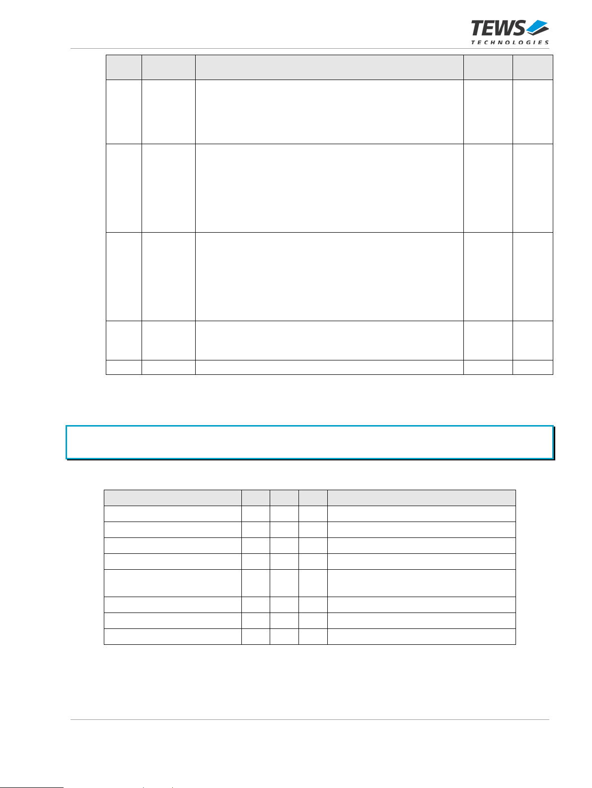
Bit Symbol Description Access Reset
No Cable (high impedance)
1 1 1
Value
11:10 RCS Receiver Clock Source
‘00’: BRG Output Clock
‘01’: external RxC Input signal
‘10’: DPLL Receive Clock
‘11’: reserved
9:7 TCS Transmitter Clock Source
‘000’: BRG Output Clock
‘001’: external RxC Input signal
‘010’: external TxC (Input direction, CCR0.TOE=0!)
‘011’: DPLL Transmit Clock
‘100’: BRG Output Clock divided by 16
others: reserved
6:4 BCS BRG Clock Source
‘000’: Oscillator 1 Clock 14.7456 MHz
‘001’: Oscillator 2 Clock 24 MHz
‘010’: Oscillator 3 Clock 10 MHz
‘011’: external RxC Input signal
‘100’: external TxC (Input direction, CCR0.TOE=0)
others: reserved
3 RTSCLK Enable TxC Output on RTS pin
‘0’: No TxC Output on RTS (normal function)
‘1’: TxC Output Enabled on RTS
2:0 MODE Transceiver Mode (M2:M0, see following table) R/W 111
R/W 00
R/W 000
R/W 000
R/W 0
Table 5-33: Additional Configuration Register
The input frequency rang e of the x4 clock multiplier is 4.5 M Hz to 28 MHz, these values must nev er
be exceeded to ensure proper function of the clock multiplier.
Transceiver Mode M2 M1 M0 Driver/Receiver Mode
Not Used (Default V.11) 0 0 0
EIA-530A 0 0 1
EIA-530 0 1 0
X.21 0 1 1
V.35 1 0 0
TxD,TxC,RxD,RxC,RTS,CTS,CD: V.11
TxD,TxC,RxD,RxC,RTS,CTS,CD: V.11
TxD,TxC,RxD,RxC,RTS,CTS,CD: V.11
TxD,TxC,RxD,RxC,RTS,CTS,CD: V.11
TxD,TxC,RxD,RxC: V.35 /
RTS,CTS,CD: V.28
EIA-449/V.36 1 0 1
V.28/EIA-232 1 1 0
TxD,TxC,RxD,RxC,RTS,CTS,CD: V.11
TxD,TxC,RxD,RxC,RTS,CTS,CD: V.28
TxD,TxC,RxD,RxC,RTS,CTS,CD: Z
Table 5-34: Physical Interface Mode Selection
TPCE863 User Manual Issue 1.0.1 Page 48 of 72
Page 49
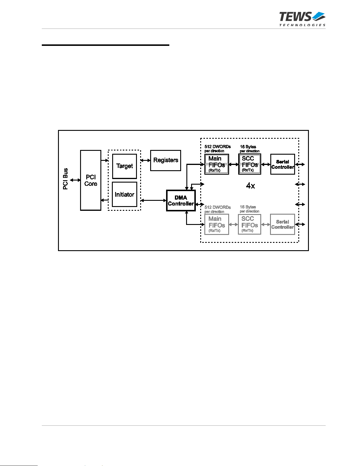
6 Functional Description
Data transfers for each direction are handled via PCI DMA transfer.
The transfers are contr olled via linked lists of desc riptors stored in host mem ory. See the following chapter
for a more detailed description of the descriptor and data structures.
The interrupt handling / operation concept is based on Interrupt Queues located in the system/shared
memory.
There is a common on-chip interrupt vector FIFO and dedicated data FIFOs for each channel and direction.
The data is not swapped by the DMA Controller, it is always stored in little endian format.
Figure 6-1 : FPGA On-Chip Block Diagram
DMA Controller 6.1
The CPU prepares linked li sts for transmit and receive channels in the shared s ystem memory. These m ay
be handled by dynam ically allocating and linking descriptor s and buffers as required during runtim e or by
static predefined memory structures e.g. ring-chained-lists (the ’last’ descriptor points back to the first
descriptor). A mix of predefined descriptor lists but dynamically handled data buffers may also be an
appropriate solution. This strategy depends on the specific application. The DMA Controller (DMAC)
provides multiple control mechanisms supporting all of these combinations in an efficient way.
The descriptors and dat a buffers can be s tored in separate m emory spaces w ithin the 32-bit a ddress range
allowing full scatter/gather methods of assembling and disassembling of packets.
Each descriptor contains a ’next descriptor address’ field to implement the linked list. Because the DMA
controller cannot distinguish between valid and invalid addresses, a ’Hold’ mechanism is implemented to
prevent the DMA controller from branching to invalid memory locations.
TPCE863 User Manual Issue 1.0.1 Page 49 of 72
Page 50
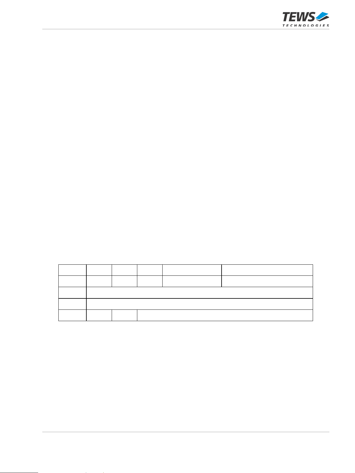
Two alternative control mechanisms are provided to detect and handle descriptor list end conditions:
DWORD
31
30
29
28..16
15..0
0
1
Next Transmit Descriptor Pointer
• Hold bit control mode (the user marks a certain descriptor with a hold flag)
• Last descriptor address contr ol mode (the user defin es a certain descriptor a ddress as a hold
condition)
The Control Mode applies to all DMA channels transmit and receive and is selected via bit ’CMODE’ in
Global Mode Register GMODE.
An HDLC frame m ay fit in one buffer connected to one des criptor or it m ay be split to sever al buffers each
associated with link ed des c riptors . A ’f r am e end’ in dica tion (FE bit) will be set in e ac h des cr ipt or which poi nts
to the last buffer of a HDLC frame.
The ’frame end’ indications are stored in the internal FIFOs and affect the FIFO control mechanisms.
Therefore descriptor ’frame end’ indications (FE bit) are also used in non frame oriented protocol modes
such as ASYNC mode. They are referred to as ’frame end/block end’ indication in the following chapters.
6.1.1 DMAC Transmit Descriptor Lists
Each transmit descriptor consists of 4 consecutive DWORDs located DWORD aligned in the shared
memory. The first 3 DW ORDs are written by the host and read by the cor responding DMA channel us ing a
burst transaction, when requested by the host either via an ’AR’ (Action Request) command or a transmit poll
command or after branching from previous transmit descriptors in the linked list. The transmit descriptor
provides information about the next descriptor in the linked list, the attached transmit data buffer address and
size, as well as some control bits.
The fourth DWORD is written by the DMA channel indicating that operation on this descriptor is finished.
The CPU will write the ad dr ess of the first descriptor of each linked list to a dedicated B ase A ddr es s R eg ister
(BTDAi) during the channe l initialization procedure. The cor responding DMA channel starts proces sing the
descriptor list by fetching the first descriptor from this address.
6.1.1.1 Transm i t De scr iptor
FE HOLD HI NO 0
2
3
FE: Frame End Bit
Indicates that the cur rent transmit data s ection (address ed by Transmit Data Po inter) contains the end of a
frame (HDLC) or the end of data block (ASYNC). When transferring the last data from this transmit data
section into the internal FIFO the DMAC marks this data with a ’frame end / block end’ indication bit.
0 C 0
Table 6-1 : Transmit Descriptor
Transmit Data Pointer
TPCE863 User Manual Issue 1.0.1 Page 50 of 72
Page 51

GMODE.CMOD = '0' (Hold Mode):
After completing a descriptor the DMAC checks the HOLD bit (previously read with the transmit descriptor). If
HOLD = 0, it branches to the next tr ansmit descr iptor. Otherwis e the correspond ing DMAC transm it channel
is deactivated as long as the host CPU does not request reactivation via the GCMDR register (either transmit
poll request or action request with ’IDT’ command).
GMODE.CMOD = '1' (Last Address Mode):
After completing a descriptor the DMAC c hecks if the first (current) transmit descr iptor address (FTDA) is
equal to the last transmit descriptor address (LT DA) stored in the corresponding channel specific on-chip
registers. When both addresses differ, it branches to the next transmit descriptor. Otherwise the
corresponding DMAC trans m it channel is deactivat ed as long as the host CPU d oes not write a ne w address
to the LTDA register or provides an action request with the ’IDT’ command.
HOLD: Hold Bit
Only valid if GMODE.CMODE = '0' (Hold Mode).
Used for descriptor list end control.
HOLD = '0':
A next descriptor is ava ilab le in th e shar ed m em ory. Af ter chec k ing the HO LD bi t the DMAC branc hes to th e
next transmit descriptor.
HOLD = '1':
The current descript or is the last one (currentl y) available for the DMAC. T he correspond ing DMAC ch annel
is deactivated for transmit direction as long as the microprocessor does not request an activation via the
CMDR register.
NO: Byte Number
NO defines the number of bytes (stored i n the data section) to be transmitted. Thus the maxim um length of
the data buffer is 8191 bytes (NO = 0x 1FFF) . A tra nsm it des criptor an d the cor res pondin g data sec tion m ust
contain at least eit her one data byte or a frame end indication. Oth erwise a DMA controller interrupt with
’ERR’ bit set is generated.
HI: Host Initiated Interrupt
If the HI bit is set, the corres ponding DMAC generat es an HI interrupt af ter transferring all dat a bytes of the
current transmit data section.
Next Transmit Descriptor Pointer:
This 32-bit pointer contains the start address of the next transmit descriptor. After fetching the indicated
number of data b ytes, the DMAC branches to the ne xt transmit descriptor. The transm it descriptor is read
entirely at the beginn ing of the transmit descriptor proces sing and is stored in on-chip mem ory. Therefore
when the DMAC bra nches to a (next) descriptor all de scriptor information m ust be valid. T his pointer is not
used if a transmitter reset or initiali zation chan nel c omm and is detec ted while the DMAC sti ll reads data from
the current transm it descriptor. In this cas e the value in the BT DA register is used as a pointer for the nex t
transmit descriptor.
The descriptor start address must be DWORD aligned.
TPCE863 User Manual Issue 1.0.1 Page 51 of 72
Page 52
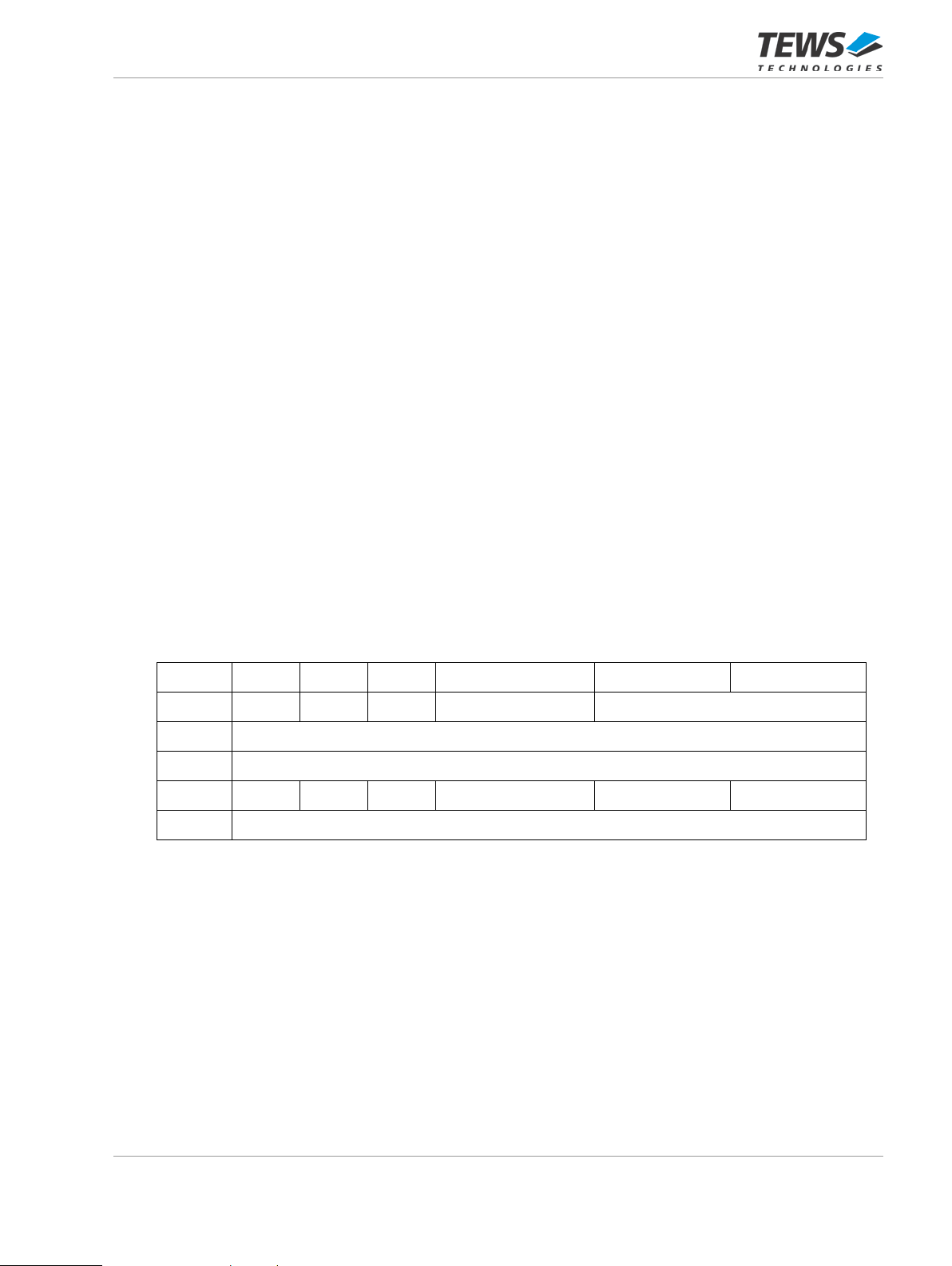
Transmit Data Pointer:
0
This 32-bit pointer contai ns the start address of the transmit data section f or a transmit desc riptor. Although
the TPCE863 works long word oriented, it is possible to begin transmit data section at byte addresses.
C: Complete Bit
This bit is set by the DMAC if
• it completes reading a data section normally
• it was aborted by a transmitter reset command.
6.1.2 DMAC Receive Descriptor Lists
Each receive descriptor c ons ists of 5 consec utive DW ORDs located DW O RD aligned in the s hared m emor y.
The first 3 DWORDs are read by the corresponding DMA channel using a burst transaction and provide
information about the nex t descriptor i n the linked list, the attached r eceive data buf fer address and s ize, as
well as some control bits.
The fourth DWO RD is written by the DMA channel in di cating that operation on th is des c riptor is f inish ed. T he
fifth DWORD is also written by the DMA channel but only for descriptors containing the first or only data
section of an HDLC frame or data block. It is a pointer to the last descriptor containing the frame or block end
(’FE’ bit) allowing the software to unchain the complete partial descriptor list containing a frame or block
without parsing through the list for ’FE’ indication.
The CPU will write the ad dr ess of the f ir st desc r iptor of eac h l ink ed list t o a de dica ted B as e A ddr ess Reg is ter
during the initializat ion procedure. The corresponding DMA channel starts operating the l inked lists at this
address.
6.1.2.1 Receive Descriptor
DWORD 31 30 29 28..16 15..8 7..0
0 HOLD HI NO 0
1
2
3
4
HOLD: Hold Bit
Only valid when GMODE.CMODE = '0' (Hold Mode)
Used for descriptor list end control.
HOLD = '0':
A next descriptor is available in the shared memory. After checking the HOLD bit the DMAC branches to next
receive descriptor
FE C 0 BNO STATUS 0
Table 6-2 : Receive Descriptor
Next Receive Descriptor Pointer
Receive Data Pointer
Frame End Descriptor Pointer
TPCE863 User Manual Issue 1.0.1 Page 52 of 72
Page 53

HOLD = '1':
The current descriptor is the last one (currently) available for the DMAC. After completion of the current
receive descriptor an inter rupt is generat ed and the corres ponding DMAC c hannel is deactivat ed for receive
direction as long as the host CPU does not request an activation via the CMDR register.
HI: Host Initiated Interrupt
If the HI bit is set , t he c orr e s pond ing DMAC gener ates an HI interrupt af ter transf erring al l data b ytes into the
current data section.
NO: Byte Number
NO defines the si ze of the recei ve data sectio n all ocated b y the host. I t has to be a m ultiple of 4 b ytes which
is the responsibility of the software. The maximum buffer length is 8188 bytes (i.e. NO = 0x1FFC).
Note that the receive data sec tion m ay need to res erve s pace f or up to 5 additi onal b ytes in HDLC m ode (32
bit CRC plus HDLCstatus byte).
Next Receive Descriptor Pointer:
This 32-bit pointer contains the start address of the next receive descriptor. After completing the current
receive descriptor the DMAC branches to the next receive descriptor to continue reception. The receive
descriptor is read entirely at the beginning of the descriptor processing and stored in on-chip memory.
Therefore when the DMAC branches to a (next) descriptor all descriptor information must be valid.
Descriptor start address must be DWORD aligned.
Receive Data Pointer:
This 32-bit pointer contai ns the start address of the receive dat a section for a receive descriptor. T he start
address must be DWORD aligned.
FE: Frame End Bit
Indicates that the current r ec eive data s ection con tains the end of a fr ame (H DLC) or the end of a dat a block
(ASYNC). This bit is set by the DMAC after transf erring the last data from the internal receive FIFO into the
receive data section. Moreover the BNO and STATUS fields are updated and the ’C’ bit is set by the DMAC.
GMODE.CMODE = '0' (Hold Mode):
After completing a d escr iptor the DM AC check s the HO LD bit (pr evi ousl y read w ith th e recei ve desc riptor ). If
HOLD = 0, it branches to th e next rec eive desc riptor . Other wise th e corr espondin g DMAC rec ei ve channe l is
deactivated as long as the host CPU does not reques t reactivation via th e GCMDR register (act ion request
with ’IDR’ command).
GMODE.CMODE = '1' (Last Address Mode):
After completing a descriptor the DMAC check s if the first (current) receive descriptor address (FRDA) is
equal to the last receive descriptor address (LRDA) stored in the corresponding channel specific on-chip
registers. When both addresses differ, it branches to the next receive descriptor. Otherwise the
corresponding DMAC r eceive c hannel is deacti vated a s long as th e host C PU does not write a new va lue to
the LRDA register or provides an action request with ’IDR’ command.
TPCE863 User Manual Issue 1.0.1 Page 53 of 72
Page 54

C: Complete Bit
7 6 5 4 3 2 1
0
RFO
CRC
RAB
This bit is set by the DMAC if:
• it completed filling the receive data section normally
• it was aborted by a receiver reset command
• an end of frame (HDLC) or end of block (ASYNC) has been stored in the receive data sec t ion .
BNO: Byte Number of Received Data
The DMAC writes the actu al number of data bytes that were stored in the current recei ve data section into
the BNO field (including CRC and status bytes).
Receive descriptor STATUS
0 0 0 0 0 0
Table 6-3 : Receive Descriptor Status Field
RA: Receive Abort
This bit indicates that the reception of a frame (HDLC) or block (ASYNC) was ended by a DMA receiver reset
command or by a HOLD bit in the current receive descriptor or by a FRDA = LRDA condition.
Frame End Descriptor Pointer:
This 32-bit pointer is only valid in the descriptor , whic h cont ains the da ta pointer to the first data s ec ti on of a n
HDLC frame or ASYNC block. This pointer is written by the DMAC with the address of the descriptor that
contains the data pointer to the last data section (FE) of the HDLC frame or ASYNC block.
RA
0
6.1.2.2 Receive Data Section Status Byte (HDLC Mode)
In HDLC protocol m ode, the last byte of a frame (Receive Status Byte, RSTA) written t o the receive data
section contains error indications caused by the SCC (e.g. CRC, receive abort, …).
7 6 5 4 3 2 1 0
1
Table 6-4 : Receive Data Section Status Byte (HDLC)
0 0 0 0
The contents of the RSTA b yte relate to the received HDLC frame and are ge nerated when end-of-fram e is
recognized at the serial receive interface.
TPCE863 User Manual Issue 1.0.1 Page 54 of 72
Page 55

RFO: Receive FIFO Overflow
A data overflow has occ ur red during reception of the f rame. Additionally, an int er rupt c an be g ener a ted ( ref er
to ISR.RFO / IMR.RFO).
CRC: CRC Compare/Check
'0': CRC check failed, received frame contains errors.
'1': CRC check OK, no errors detected in received frame.
RAB: Receive Message Aborted
The received fram e was aborted from the tra nsmitting station. Accordin g to the HDLC protocol, th is frame
must be discarded by the receiver station.
6.1.2.3 Receive Data Section Status Byte (ASYNC Modes)
In ASYNC protocol mode a stat us byte ca n be attache d additiona lly to ever y s tored data byte (CCR 2.RFDF
= '1').
The data character and status character format is determined as follows:
15 14 13..9 8 7..0
parity
error
frame
error
reserved
Table 6-5 : Receive Data Section Status Byte (ASYNC)
parity
bit
data byte
DMAC Interrupt Cont roller 6.2
The interrupt conce pt is bas ed on 32-b it interr upt vector s generated by the d ifferent b locks . Interrupt vec tors
are stored in a com m on on -chip interrupt FIFO wh ich i s 32 DW ORDs deep. T he inter rupt c ontro ller tr ansf ers
interrupt vectors t o one of nine c ircular interr upt queu es loca ted in the s har ed s ystem m emor y depending o n
the source ID of each interrupt vector.
In addition new i nterrupt ve ctors are ind icate d in t he gl obal stat us r egister GST AR on a per queue bas is and
selectively confirm ed by writing ’1’ to the cor responding GST AR bit positions. T he PCI interrupt signal INT A
is asserted with any new interrupt event and remains asserted until all events have been confirmed.
Each interrupt queue length and memory location can be configured via specific interrupt queue base
address registers and two shared interrupt queue length registers. The queue length is individually
programmable in multiples of 32 DWORDs (see IQLENR0/1 registers).
One dedicated interr upt queue is pr ovided per SC C channel and direction ( IQSCCiRX and IQ SCCiTX) . Non
channel specific interrupt vectors generated by the DMAC are transferred to the configuration queue IQCFG.
The internal blocks provide mask registers for suppressing interrupt indications. Masked interrupts will
neither generate an interrupt vector nor an INTA signal or GSTAR indication.
TPCE863 User Manual Issue 1.0.1 Page 55 of 72
Page 56

6.2.1 DMA Controller initiated Interrupts
The DMA interrupt c ontroller generates channe l/direction specific interrupts regarding transmit and receive
descriptor handling:
Host Initiated interrupt (HI):
This interrupt can be forc ed by setting bit ’ HI’ in the rec eive or trans m it desc riptor. In this c ase the DM AC will
generate an HI-inter rupt with com pletio n of th is desc rip tor i.e. when t he DM AC is ready to branc h to the nex t
descriptor address. T his might be used to monitor the progres s of the corresponding DMA channe l on the
descriptor list. As an exam ple t he HI interr upt ca n be us ed to d ynam ically reques t attachment of new receive
descriptors to the list if the DMA channel comes close to the list end.
Frame Indication interrupt (FI):
This interrupt is gener ated with completion of any receive or trans mit descriptor with a s et ’frame end/block
end’ indication, i.e. FE=’1’.
Error interrupt (ERR):
Indicates an unexpected descriptor configuration
Receive descriptor:
ERR is generated if receiv e data cann ot be tr ansfer red to the s hared m em or y completel y beca use the f rame
(block) does not fit into the cur rent data section and a HO LD condition (HO LD bit or LRDA=FRD A) prevents
the DMAC from branching to the next descriptor.
ERR is also generated if an already started DMA transfer is aborted by a receive DMA reset (RDR)
command.
Transmit descriptor:
In transmit direction an ERR interrupt is generated if one of the following descriptor settings is detected
- HOLD=’1’ and FE=’0’ (the already started transmit frame could not be finished)
- LTDA=FTDA and FE=’0’ (the already started transmit frame could not be finished)
- FE=’0’ and NO=’0’ (a packet of length 0 is supposed to be a ’frame’ with FE bit set)
The DMA controller will con tinue ’ norm al’ operat ion in c ase of an ERR e vent. N ever theless these cas es m a y
result in receive data overflows or transmit data underruns.
FI and HI interrupt indications cause d by one descriptor will be generated into one interrupt vector with ’HI’
and ’FI’ bit set.
TPCE863 User Manual Issue 1.0.1 Page 56 of 72
Page 57
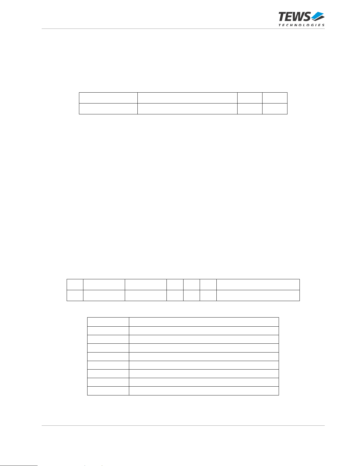
6.2.2 Interrupt Vector Description
1010
Source-ID
Description
6.2.2.1 Configuration Inte r r upt V ector
Configuration interrup t vectors are transferred to the Configuration Interrupt Queue ’IQCF G’ in the shared
memory.
31..28 27..2 1 0
Source ID =
Table 6-6 : Configuration Interrupt Vector
ARF: Action Request Failed Interr up t
This bit indicates that an action request command was completed with an ’action request failed’ condition:
ARF = '0': No action request was performed or no ’action request failed’ condition occurred
completing an action request.
ARF = '1': The last action request command was completed with an ’action request failed’ condition.
ARACK: Action Request Acknowledge Interrupt
This bit indicates that an action request command was completed successfully:
ARACK = '0': No action request was performed or completed successfully.
ARACK = '1': The last action request command was completed successfully.
0 ARF ARACK
6.2.2.2 DMA Controller Interrupt Vector
DMA controller interrupt v ectors are tr ansferred to the cor responding channe l and directio n specific interru pt
queues IQSCCiRX and IQSCCiTX respectively.
31 30..28 27..19 18 17 16 15..0
0 Source ID 0 HI FI ERR 0
Table 6-7 : DMA Interrupt Vector
000 Receive Channel 0 Interrupt Vector (IQSCC0RX)
001 Receive Channel 1 Interrupt Vector (IQSCC1RX)
010 Receive Channel 2 Interrupt Vector (IQSCC2RX)
011 Receive Channel 3 Interrupt Vector (IQSCC3RX)
100 Transmit Channel 0 Interrupt Vector (IQSCC0TX)
101 Transmit Channel 1 Interrupt Vector (IQSCC1TX)
110 Transmit Channel 2 Interrupt Vector (IQSCC2TX)
111 Transmit Channel 3 Interrupt Vector (IQSCC3TX)
Table 6-8 : DMA Interrupt Vector Source-IDs
TPCE863 User Manual Issue 1.0.1 Page 57 of 72
Page 58

HI: Host Initiated interrupt (Rx/Tx Channel)
This bit indicates tha t a Host Initiat ed (HI) interrup t occurred, i. e. the correspon ding DMA contro ller channel
detects the ’HI’ bit set to ’1’ in the receive or transmit descriptor before branching to the next descriptor.
HI=’0’ No Host Initiated (HI) interrupt is indicated by this vector.
HI=’1’ A Host Initiated (HI) interrupt is indicated by this vector.
FI: Frame Indication interrupt (Rx/Tx Channel)
This bit indicates that a Frame Indication (FI) interrupt occurred.
Receive direction:
FI=’1’ indicates, that a frame has been received completely or was stopped by a DMAC receiver reset
command or a hold cond ition set in a receive desc riptor. It is set when the DMAC branches from the last
descriptor belonging to th e current frame (or block) (FE=’1’) to the first descriptor of a new fram e. It is also
set when the descriptor in which the frame/block is finished contains a hold condition.
Transmit direction:
Issued if the ’FE’ bit is detected in th e transmit descriptor. It is set when the DMAC branc hes to the next
transmit descriptor, belonging to a new fram e or when ’HOLD’ bit is set in conjunction with ’FE’ bit. ’ERR’
indication (without ’FI’) is set, if a transmit descriptor contains a ’HOLD’ (hold condition) but no ’FE’ bit.
FI=’0’ No Frame Indication (FI) interrupt is indicated by this vector.
FI=’1’ A Frame Indication (FI) interrupt is indicated by this vector.
ERR: ERROR Indication interrupt (Rx/Tx Channel)
This bit indicates that an Error interrupt occurred.
Receive direction:
Issued if the curre nt frame/block could not be tr ansferred to the shared m emory completely, because of a
hold condition in a rec eive descr iptor not prov iding enough b ytes for the fr ame/block or the fram e/block was
aborted by a DMAC receiver reset command.
Transmit direction:
Issued if a transm it descriptor contains a hold condition but FE =’0’ or if the last descriptor had NO=0 a nd
FE=’0’.
ERR=’0’ No Error (ERR) interrupt is indicated by this vector.
ERR=’1’ An Error (ERR) interrupt is indic ate d b y this vect or.
TPCE863 User Manual Issue 1.0.1 Page 58 of 72
Page 59
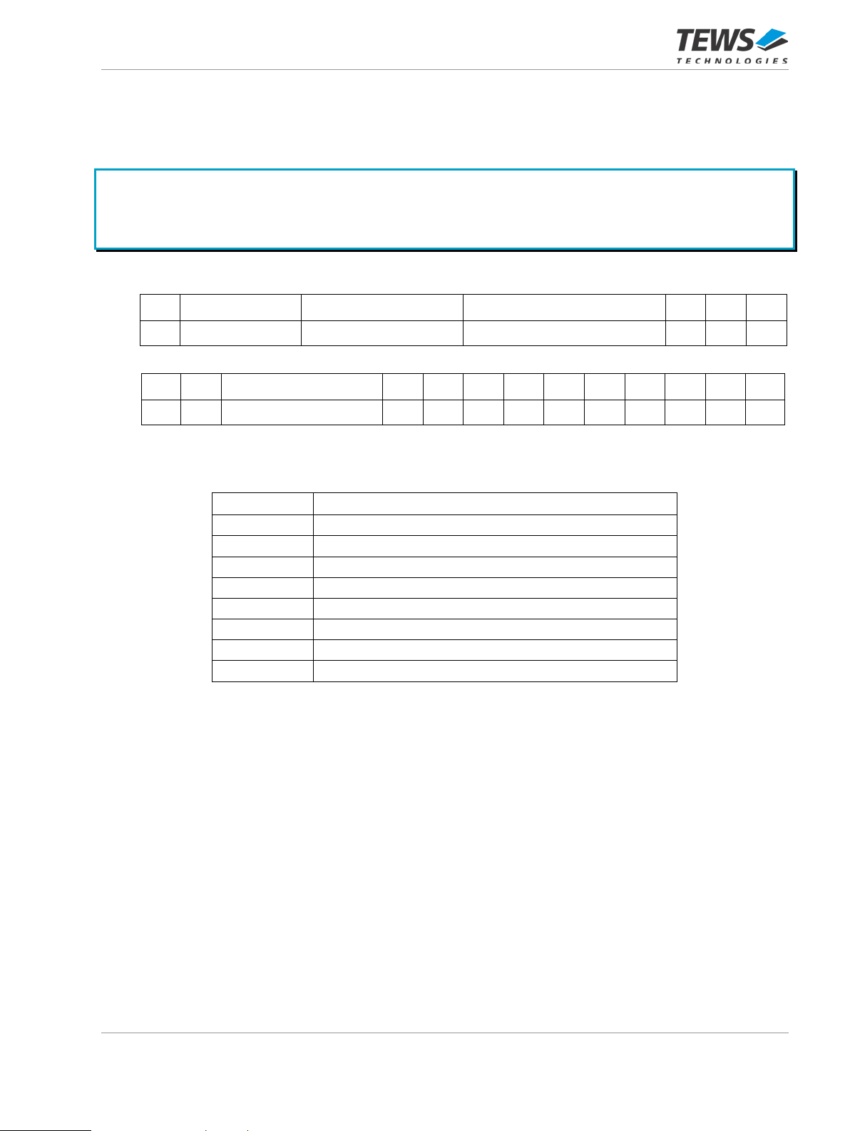
6.2.2.3 SCC Interrupt V ector
31
30..28
27..24
23..19
18
17
16
15
14
13..10
9 8 7 6 5 4 3 2 1
0
0 CSC 0 BRK BRKT
TCD TIME
PERR
FERR
PLLA
CDSC
R
Serial Channel (SCC) relat ed interrupt vectors are transferred to the corresponding channel and direction
specific interrupt queues IQSCCiRX and IQSCCiTX respectively.
Interrupt vectors generated by the SCCs might contain interrupt indications for both, receive AND
transmit direction. But in receive interrupt queues only the receive interrupt indications need to be
served and in transmit interrupt queues only transmit interrupt indications need to be served by the
software.
0 Source ID 0010 0 ALLS 0 XDU
FO 0
Table 6-9 : SCC Interrupt Vector
Source-ID Description
000 Receive Channel 0 Interrupt Vector (IQSCC0RX)
001 Receive Channel 1 Interrupt Vector (IQSCC1RX)
010 Receive Channel 2 Interrupt Vector (IQSCC2RX)
011 Receive Channel 3 Interrupt Vector (IQSCC3RX)
100 Transmit Channel 0 Interrupt Vector (IQSCC0TX)
101 Transmit Channel 1 Interrupt Vector (IQSCC1TX)
110 Transmit Channel 2 Interrupt Vector (IQSCC2TX)
111 Transmit Channel 3 Interrupt Vector (IQSCC3TX)
Table 6-10: SCC Interrupt Vector Source-IDs
Bit field [18:0] of the SC C interrupt vector is a copy of the SCC Interrupt Status Register ISR (f or detailed
information see chapter ‘ISR - Interrupt Status Register’).
TPCE863 User Manual Issue 1.0.1 Page 59 of 72
Page 60
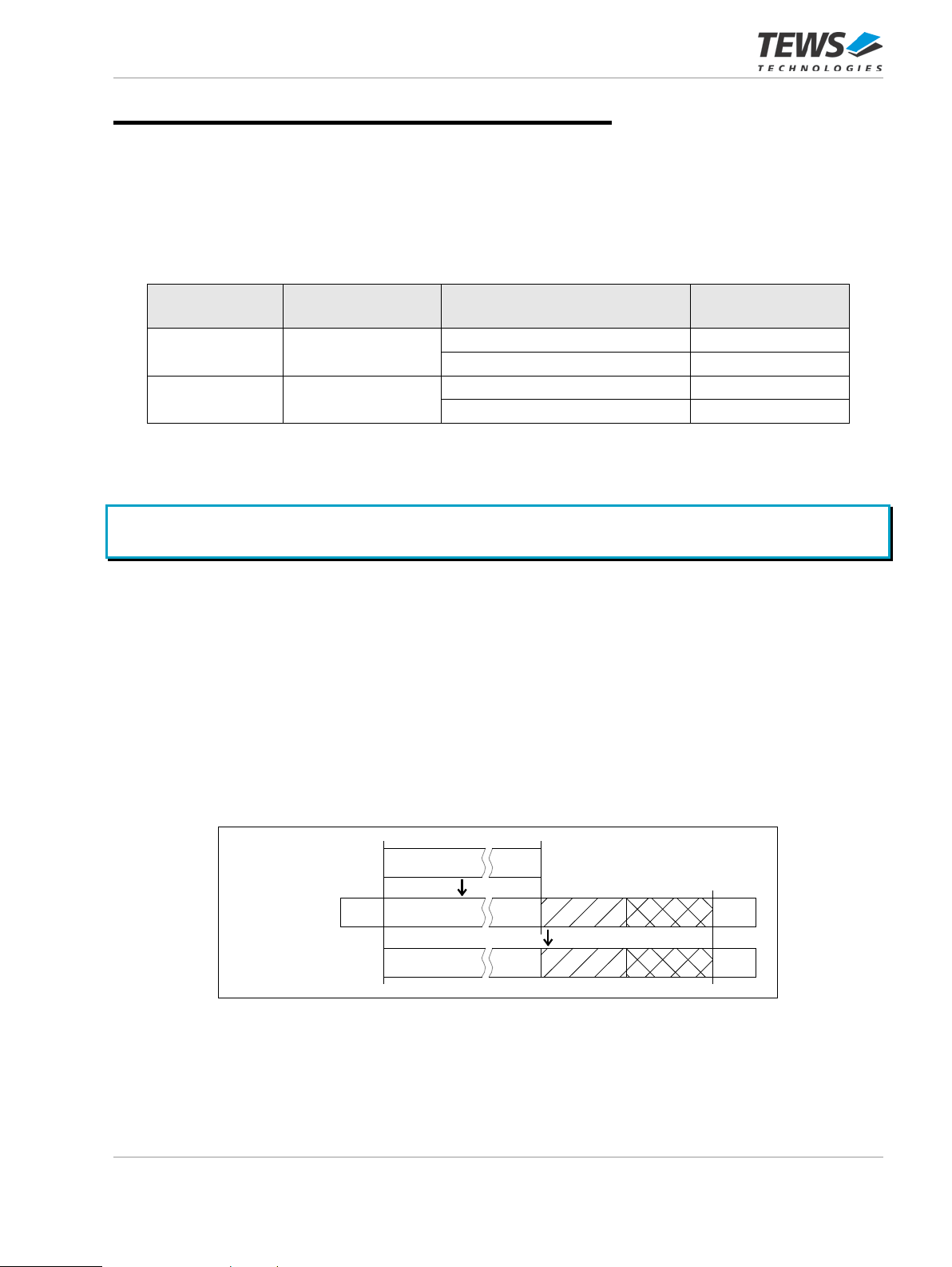
7 Serial Communication Controller
Engine
Setting
Setting
Flag
Flag
data
CRC-16 CRC-32
RSTA
data
CRC-16 CRC-32Data in Receive FIFO
Transmitted /
Received
Data Stream
data
Data in Transmit FIFO
Protocol Description 7.1
The following tabl e provides an overview of all suppor ted protocol m odes and th eir assignm ent to the m ajor
protocol engines HDLC and ASYNC. The protocol engine of each SCC is selected via bit field ’SM’ in
register CCR0. The Sub Modes are selected via additional bit fields in registers CCR0 and CCR1.
Protocol
CCR0 Register
Protocol Mode
CCR1 Register
HDLC SM = ‘00’
ASYNC SM = ‘11’
Table 7-1 : Protocol Modes
Extended transparent is a fully bit-transparent transmit/reception mode which is treated as a submode of the HDLC block.
HDLC Address Mode 0 MDS = ‘10’
Extended Transparent Mode MDS = ‘11’
Asynchronous Mode BCR = ‘1’
Isochronous Mode BCR = ‘0’
7.1.1 HDLC Mode
The HDLC transmitter does not generate shared f lags or shared zeroes between flags. T he HDLC receiver
supports shared flags and shared zeroes between flags.
7.1.1.1 Address Mode 0
Standard HDLC fr aming and bit-stuffing is perform ed by the transm itter. There is an option to append 16 bit
or 32 bit CRC data for each frame.
The receiver will store the frame data (including CRC) plus a status byte.
TPCE863 User Manual Issue 1.0.1 Page 60 of 72
Figure 7-1 : HDLC Address Mode 0
Page 61

7.1.1.2 Extended Transparent Mode
In extended transparent mode, fully transparent data transmission/reception without HDLC framing is
performed (i.e. without FL AG generation /rec ognition, C RC gener ati on/check , or bit s tuff ing). T his allows us er
specific protocol variations.
7.1.2 Asynchronous (ASYNC) Mode
Character framing is achi eved by start and stop bits. Each d ata character is preceded b y one start bit and
terminated by one or two st op bits. The c haracter lengt h is selectab le from 5 to 8 bits. Optiona lly, a parit y bit
can be added which c omplements the number of ones to an even or odd quantity (even/od d parity). The
parity bit can also b e pro gramm ed to hav e a fix value (Mark or Space). T he char acter form at c onfigurati on i s
performed via appropriate bit fields in register CCR2.
7.1.2.1 Asynchronous Mode
NRZ data encoding and Bit clock rate x16 (register CCR0, bit BCR = ‘1’) shall be selected (register CCR0, bit
field ’SC’).
The transmitter operates at a clock rate which is 16 tim es the nominal data bit rate. T he generated data bit
rate is 1/16 of the transmit clock rate.
The receiver operates at a clock r ate which is 16 tim es the nominal (ex pected) data b it rate. It s ynchronizes
itself to each charac ter b y detecting and verif ying the s tar t bit . Ov er s ampling (3 samples) ar ound the nominal
bit center in conjunction with majority decision is provided for every received bit (including start bit).
The synchronization lasts for one character; the next incoming character causes a new synchronization. As a
result, the demand f or hig h clock accurac y is reduc ed. T wo comm unication sta tions us ing the asynchrono us
procedure are clock ed independently; their clocks need n ot to be in phase or locked to exac tly the same
frequency but, in fact, may differ from one another within a certain range.
7.1.2.2 Isochr onous Mode
Bit clock rate x1 shall be selected (register CCR0 bit BCR = ‘0’).
The isochronous mode uses the asynchronous character format. However, each data bit is only sampled
once (no oversampling) . The input clock has to be externally phas e locked to the data stream. This m ode
allows much higher transfer rates.
7.1.2.3 Receive Data Storage
If the receiver is ena bled, received data is stor ed in the receive FIFO (the LSB is received firs t). Character
length, number of stop bits and the optional parity bit are checked. Errors are indicated via interrupts.
Additionally, the charac ter specific error status (framing and parit y) can optionally be stored in the receive
FIFO. Filling of the receive FIFO is controlled by
- a programmable threshold level (bit field ’RFTH’ in register CCR2),
- the selected data format (bit ’RFDF’ in register CCR2),
- detection of the programmable Termination Character (bit ’TCDE’ and bit field ’TC’ in register TCR).
Additionally, the time-out event interrupt as an o ptional status information indica tes that a certain time has
elapsed since the reception of the last character (refer to register CCR1).
TPCE863 User Manual Issue 1.0.1 Page 61 of 72
Page 62

7.1.2.4 Data Transmission
The selection of asynchronous or isochronous operation has no further affect on the transmitter. The bit
clock rate is solely a dividing factor for the selected clock source.
Transmission of the contents of the transmit FIFO starts after providing data to the DMA controller. The
character frame f or each character, cons isting of start bit, the character itse lf with defined charac ter length,
optionally generated parity bit and stop bit(s) is assembled.
After finishing transm ission (indicated by the ‘ALLS’ interrupt), IDLE sequence (lo gical ‘1’) is transmitted on
transmit pin TxD.
Additionally, the CTS signal may be used to control data transmission.
7.1.2.5 Break Detection/Generation
Break generation:
On generating the transmit break comm and (bit ’XBR K’ in re gist er CCR 2), t he T xD p in is imm ediatel y forc ed
to physical ‘0’ level with the next following clock edge, and released with the first clock edge after this
command is reset again by software.
Break detection:
The SCC recognizes the br eak c ondition upon rec eiving c onsecutive (ph ysical) ‘0 ’s f or the defined charac ter
length, the optional parity and the selected number of stop bits (‘zero’ character and framing error). The
‘zero’ character is not push ed to t he rec e ive F IF O. The ’Break’ interrupt (BR K) is generated (if enabled). The
break condition will be pres ent until a ‘1’ is received which is indicated b y the ‘Break Terminated’ interrupt
(BRKT).
7.1.2.6 Flow Control
Transmitter:
The transmitter outp ut is enab led if CTS sig nal is ‘LOW ’. Setting bit C CR1.FCTS = ‘1’ allo ws the transm itter
to send data independent of the condition of the CTS signal.
Receiver:
For some applications it is desirable to provide means of flow control to indicate to the far end transm itter
that the local receiver’s buffer is getting full.
This flow control can be us ed between two DTEs and bet ween a DTE and a DCE (MODEM) that s upports
this kind of bi-directional flow control.
Setting bit CCR1.FRTS = ‘ 1’ and CCR1.RTS = ‘0’ invok es the receiver flow control. W hen the SCC receive
FIFO data-count reac hes the upper thr eshold of 12 bytes (16 bytes total), the RTS signal is forced inactive
(HIGH). When the receiv e FIFO dat a-count is les s or equal to t he lower thres hold of 4 bytes, the RT S signal
is re-asserted (‘LOW ’). Note that data is immediately transferred from the SCC receive FIFO to the DMA
accessible FIFO (as long as ther e is space av ailable). T hus when the SCC receive FIFO r eaches the u pper
threshold, there are 4 more bytes storage a vailable before an overf low may occur. This provides sufficient
time for the far end transmitter to react to the change in the RTS signal and stop sending more data.
TPCE863 User Manual Issue 1.0.1 Page 62 of 72
Page 63
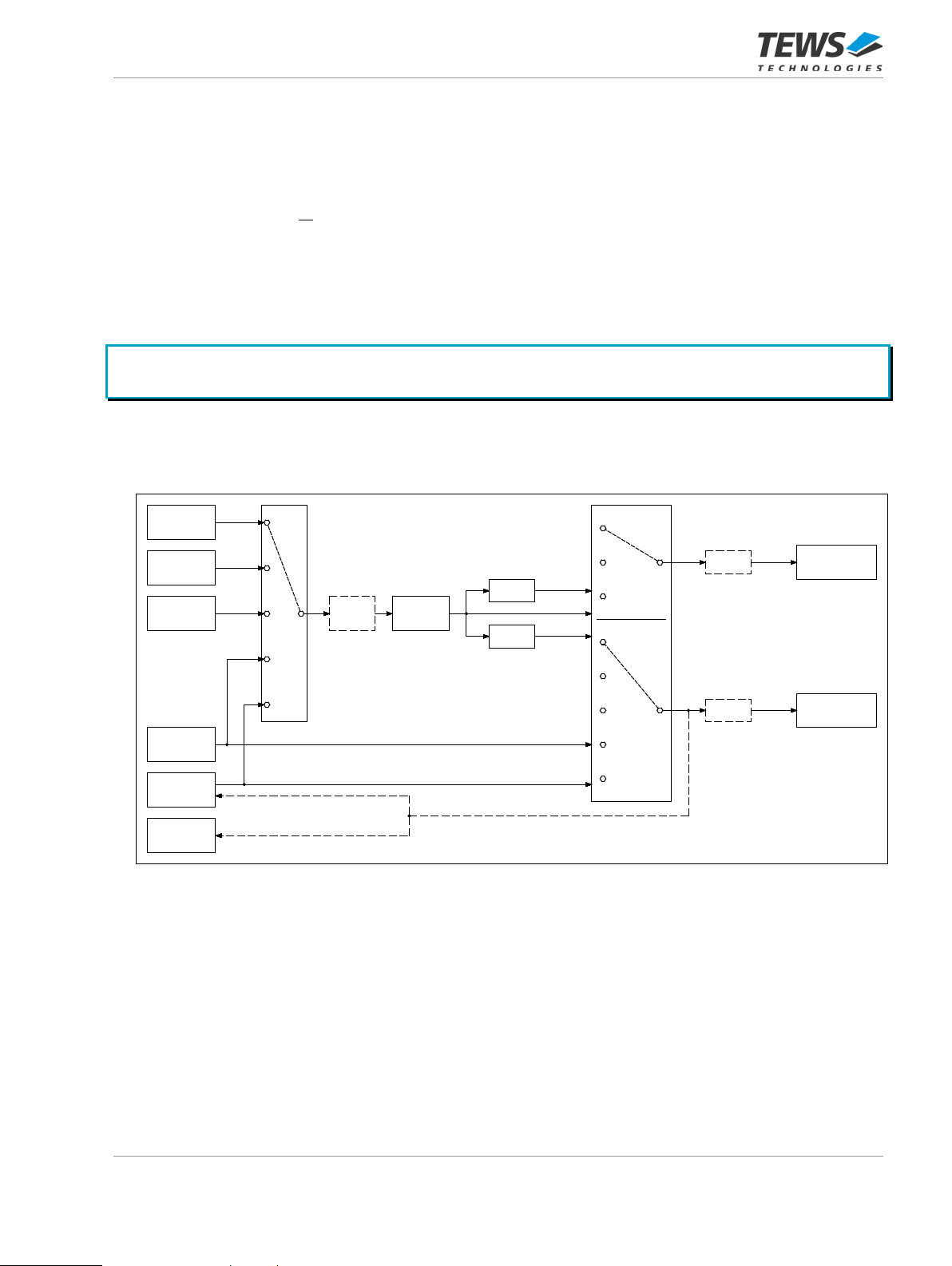
Clock Sources 7.2
O s c illa to r 2
24 MHz
O s c illa to r 1
14.7456 MHz
O s c illa to r 3
10 MHz
external
TxCLK
external
RxCLK
internal
TxCLK
RTS
Transmitter
Receiver
Inverter
(optional)
BRG
Baud Rate Generator
internal
RxCLK
TxCLK m onitor signal
(optional)
Inverter
(optional)
DPLL
16:1
f
DPLL
f
BRG
f
BRG/16
f
RxCLK
f
TxCLK
f
DPLL
f
BRG
f
RxCLK
f
BRG/16
f
BRG
f
DPLL
f
RxCLK
f
TxCLK
x4
Clock Multiplier
(optional)
TxCLK m onitor signal
(optional)
The TPCE863 suppor ts se veral c lock sourc es f or the trans m itter and rec eiver cir cuits , contro lled b y the A CR
register. Clock source options are three on board oscillators (14.7456 MHz, 24 MHz and 10 MHz), the
external RxCLK and TxCLK inputs or the internal clock recovery circuit (DPLL). T xCLK can be an input for
the internal transmit clock or an output providing a transmit clock monitor signal (see following figure).
The guaranteed max imum data rate is limited by the m ultiprotocol transceivers and is at least 10 Mbit/s in
EIA-530 (V.11) and V.35 transceiver modes. Maximum data rate of EIA-232 (V.28) is 115.2 kbit/s. The
maximum data rate in asynchronous mode with over sampling or synchronous DPLL m ode is 2 Mbit/s. To
generate higher internal clock frequencies for oversampling or DPLL reference cloc k, an optional x4 clock
multiplier is provided.
The input frequency range of the internal x4 clock multiplier is 4.5 MHz to 28 MHz, these values must
never be exceeded to ensure proper functio n o f the clock multiplier.
Figure 7-2 : Clock Sources
Baud Rate Generation 7.3
Each of the four channels has its own Baud Rate Generator (BRG), controlled by the BRR registers
(0x012C, 0x01AC, 0x022C, 0x02AC).
The Baud Rate Generator output clock frequency is: f
The baud rate generator input clock f
depends on the selected clock source (see also previous chapter
in
“Clock Sources”).
The divisor k can be set in 2 ways, determined by BRR[31].
TPCE863 User Manual Issue 1.0.1 Page 63 of 72
= fin / k.
BRG
Page 64
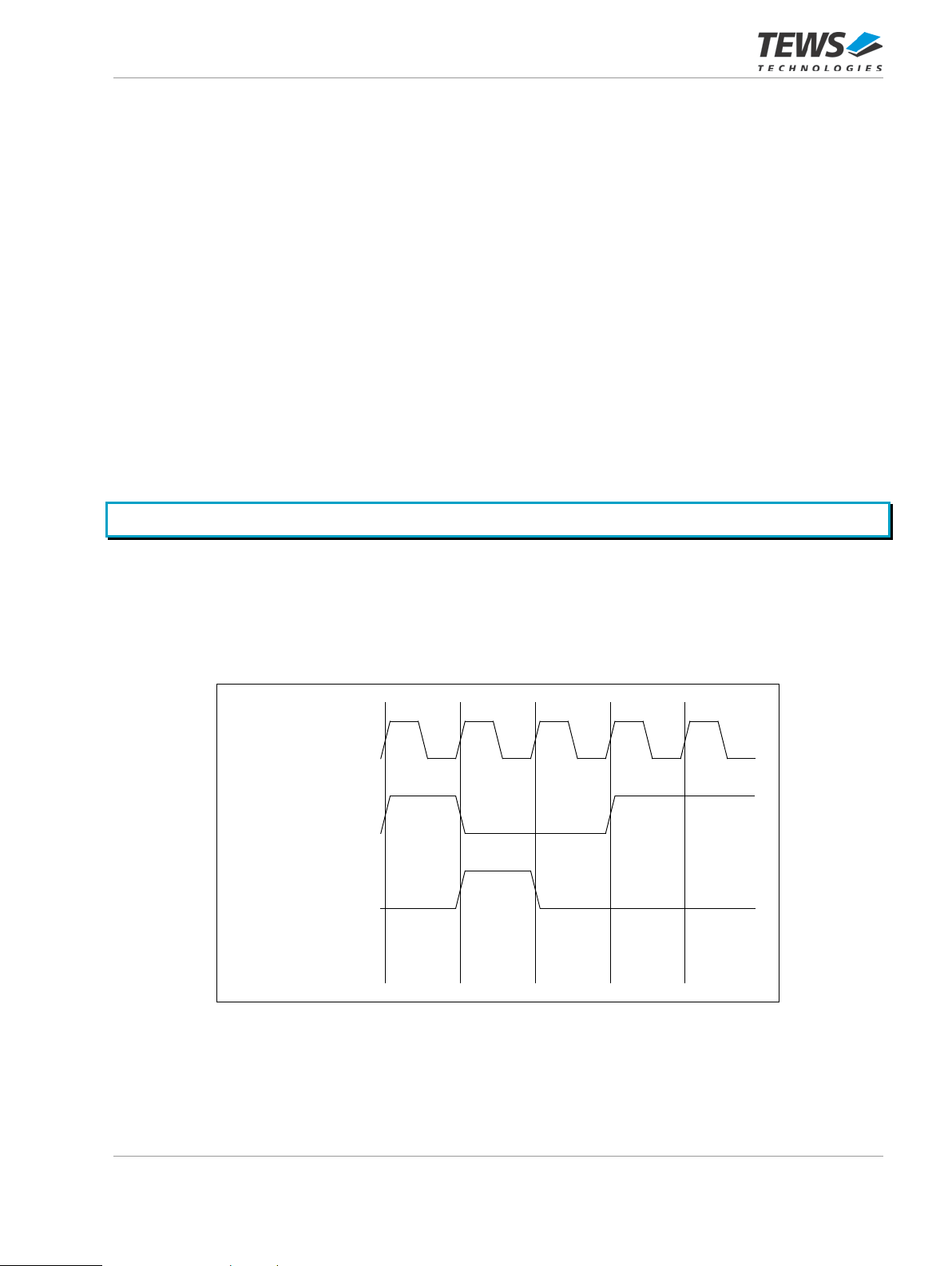
When BRR[31] = 0, k is calculated as follows:
Transmit /
Receiver Clock
NRZ
1 0 0
1 10
NRZI
M
k = ( N + 1 ) × 2
with N (BRR[5:0]) = 0..63 and M (BRR[11:8]) = 0..15
The alternative is to set (k – 1) directly as a 21-bit wide value, when BRR[31] = 1:
k = BRR[20:0] + 1
Data Encoding 7.4
The following codings of the serial data are supported:
• Non-Return-To-Zero (NRZ)
• Non-Return-To-Zero-Inverted (NRZI)
• FM0 (known as Bi-Phase Space)
• FM1 (known as Bi-Phase Mark)
• Manchester (known as Bi-Phase)
NRZ data encoding must be used for asynchronous mode.
7.4.1 NRZ and NRZI Encoding
NRZ: The signal level corresponds to the value of the data bit.
NRZI: A logical ‘0’ is indicated by a transition and a logical ‘1’ by no transition at the beginning of the bit cell.
Figure 7-3 : NRZ and NRZI Data Encoding
TPCE863 User Manual Issue 1.0.1 Page 64 of 72
Page 65
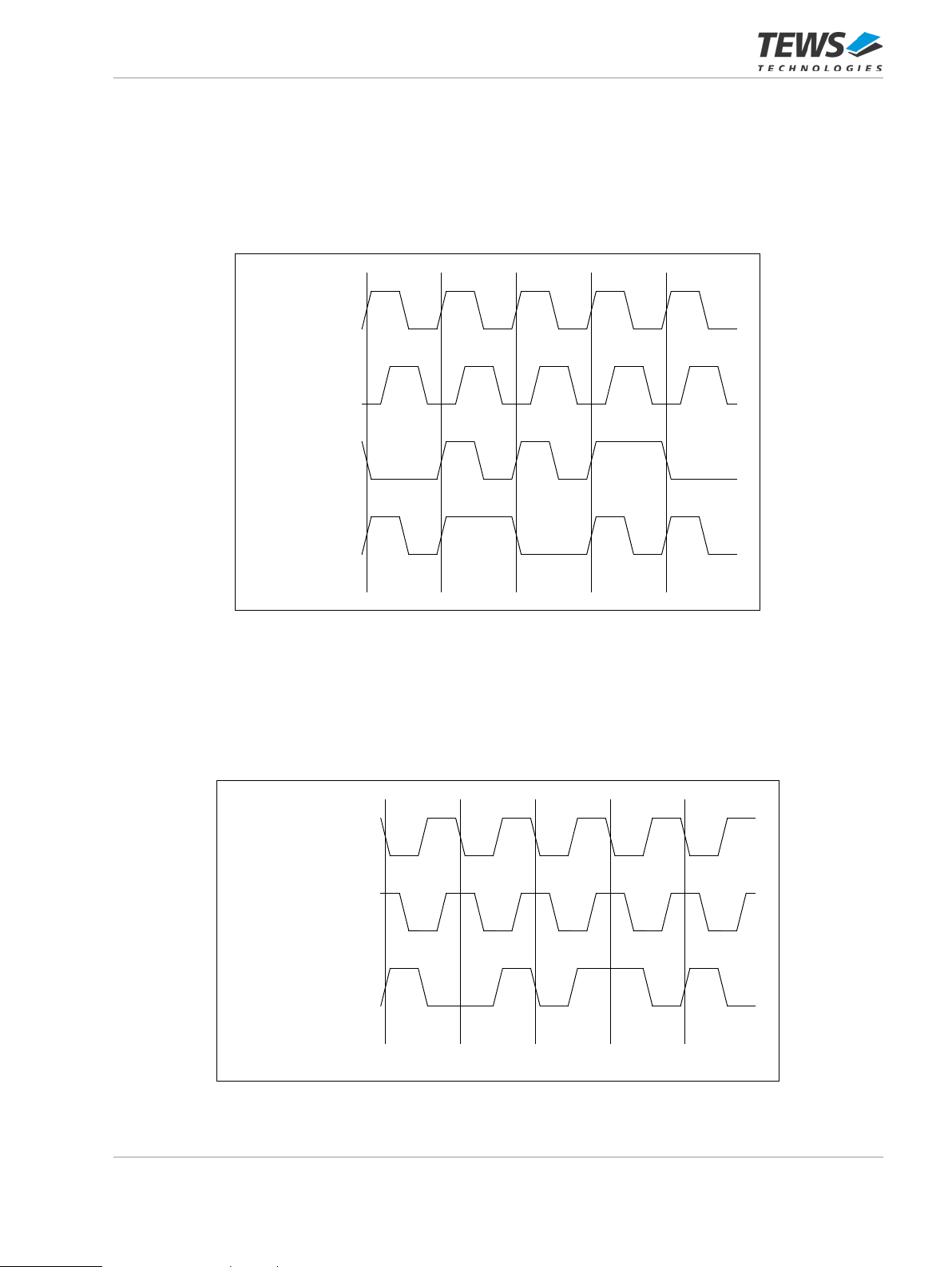
7.4.2 FM0 and FM1 Encoding
Transmit
Clock
FM0
1
0 0 1 1
Receiver
Clock
FM1
Transmit
Clock
Manchester
1 0 0 1
1
Receiver
Clock
FM0: An edge occ urs at the beginning of every bit cell. A logical ‘0 ’ has an additional edge in the c enter of
the bit cell, whereas a logical ‘1’ has none. The transmit clock precedes the receive clock by 90°.
FM1: An edge occ urs at the beginning of every bit cell. A logical ‘1 ’ has an additional edge in the c enter of
the bit cell, whereas a logical ‘0’ has none. The transmit clock precedes the receive clock by 90°.
Figure 7-4 : FM0 and FM1 Data Encoding
7.4.3 Manchester Encoding
In the first half of the bit cell, the physica l signal leve l corresponds to the log ical value of the data bit. At the
center of the bit cell this level is inverted. The transmit clock precedes the receive clock by 90°.
TPCE863 User Manual Issue 1.0.1 Page 65 of 72
Figure 7-5 : Manchester Data Encoding
Page 66

Clock Recovery (DP LL) 7.5
FM0, FM1 and Manc hester data encod ings are eliminatin g the need to trans fer additional cloc k information
via a separate ser ial cl ock line (s o ther e is n o add ition al c lock signal tr ansf erred along with t he dat a stream ).
Instead the clock signal is recovered from the receive data stream by the use of the internal DPLL circuit.
The main task of the DPLL (digita l-phase-locked-loop) is to derive the r eceive clock from the incom ing data
stream and to adjust its phase to the incoming data in order to provide optimal bit sampling.
The DPLL reference clock is the baud rate generator output clock which m ust be set to be 16 times the
expected data rate. The receive clock source must be set to ‘DPLL ’ (ACR.RCS = ‘10’). T he transmit clock
source may set to b e the baud rate generator o utput clock divided by 16 ( ACR.TCS = ‘100’) or to be t he
transmit clock generated by the DPLL circuit (ACR.TCS = ‘011’).
The mechanism for the DPLL clock recovery depends on the selected data encoding (se e chapter “Data
Encoding”).
TPCE863 User Manual Issue 1.0.1 Page 66 of 72
Page 67

8 Configuration Hints
Byte 3
AD[31..24]
Big / Little Endian 8.1
PCI – Bus (Little Endian):
Byte 0 AD[7..0]
Byte 1 AD[15..8]
Byte 2 AD[23..16]
The TPCE863 expects all access es by the host/C PU and all data stru ctures in the ho st/system RAM
to be ‘Little Endian’.
Transmit data in lower bytes is sent first.
Receive data that was received earlier is stored at lower bytes.
Configuration EEPROM 8.2
An industry standard M93C56 2 Kbit serial EEPROM is connected to the FPGA and can be accessed
through the GCTLR register. The EEPROM is configured for word (16 bit) accesses.
Addresses 0x00...0x5F ar e factory programmed with configuration information u sed by the software drivers
and must not be overwritten.
The other addresses (0x60...0x7F) are user programmable.
The configuration EEPROM contains the following data:
• Vendor ID
• Vendor Device ID
• Subsystem Vendor ID
• Subsystem Device ID
• The module version and revision
• The oscillator frequencies in Hz
• The physical interface attached to the serial channels
• The maximal baud rate of the transceivers in bps
• The supported control signals of the serial channels
For the physical interfaces and the control signals applies: Bit 3 represents UART channel 3 and bit 0
represents UART c hannel 0. The ap propri ate bit is set to ‘1’ f or e ach U ART channel attach ed to the phys ical
interface represented by the word. Bit 15 to bit 4 are always ‘0’.
TPCE863 User Manual Issue 1.0.1 Page 67 of 72
Page 68

Address
Configuration Register
TPCE863
0x00 Vendor ID 0x1498
0x01 Device ID 0x735F
0x02 Subsystem Vendor ID 0x1498
0x03 Subsystem ID 0x700A
0x04 Module Version 0x0100
0x05 Module Revision 0x0000
0x06 Module Variant 0x700A
0x07 EEPROM Revision 0x0001
0x08 Oscillator 1 Frequency (high) 0x00E1
0x09 Oscillator 1 Frequency (low) 0x0000
0x0A Oscillator 2 Frequency (high) 0x016E
0x0B Oscillator 2 Frequency (low) 0x3600
0x0C Oscillator 3 Frequency (high) 0x0098
0x0D Oscillator 3 Frequency (low) 0x9680
0x0E-0x0F Reserved -
0x10 RS232 Channels 0x000F
0x11 RS422 Channels 0x000F
0x12-0x14 Reserved -
0x15 Multiprotocol Channels
0x16-0x1E Reserved -
0x1F Programmable Interfaces 0x000F
0x20 Max Data Rate RS232 (high) 0x0001
0x21 Max Data Rate RS232 (low) 0xF400
0x22 Max Data Rate RS422 (high) 0x0098
0x23 Max Data Rate RS422 (low) 0x9680
0x24-0x2F Reserved -
0x30 RxD & TxD 0x000F
0x31 RTS & CTS & CD 0x000F
0x32 Full modem 0x0008
0x33-0x5F Reserved 0x60-0x7F
User programmable space
0x000F
-
The Rx-/Tx-Clock and Data I/O lines are connected to LTC2846 transceiver s with on-c hip ter mination.
The control I/O lines (RTS, CTS, CD) are connected t o LTC2844 transceivers without on-chip terminati on, as
termination of these signals is not necessary in the normal case. If the application requires on board
termination for these lines please contact TEWS TECHNOLOGIES.
TPCE863 User Manual Issue 1.0.1 Page 68 of 72
Table 8-1 : Configuration EEPROM Data
Additional Termination Resistors 8.3
Page 69
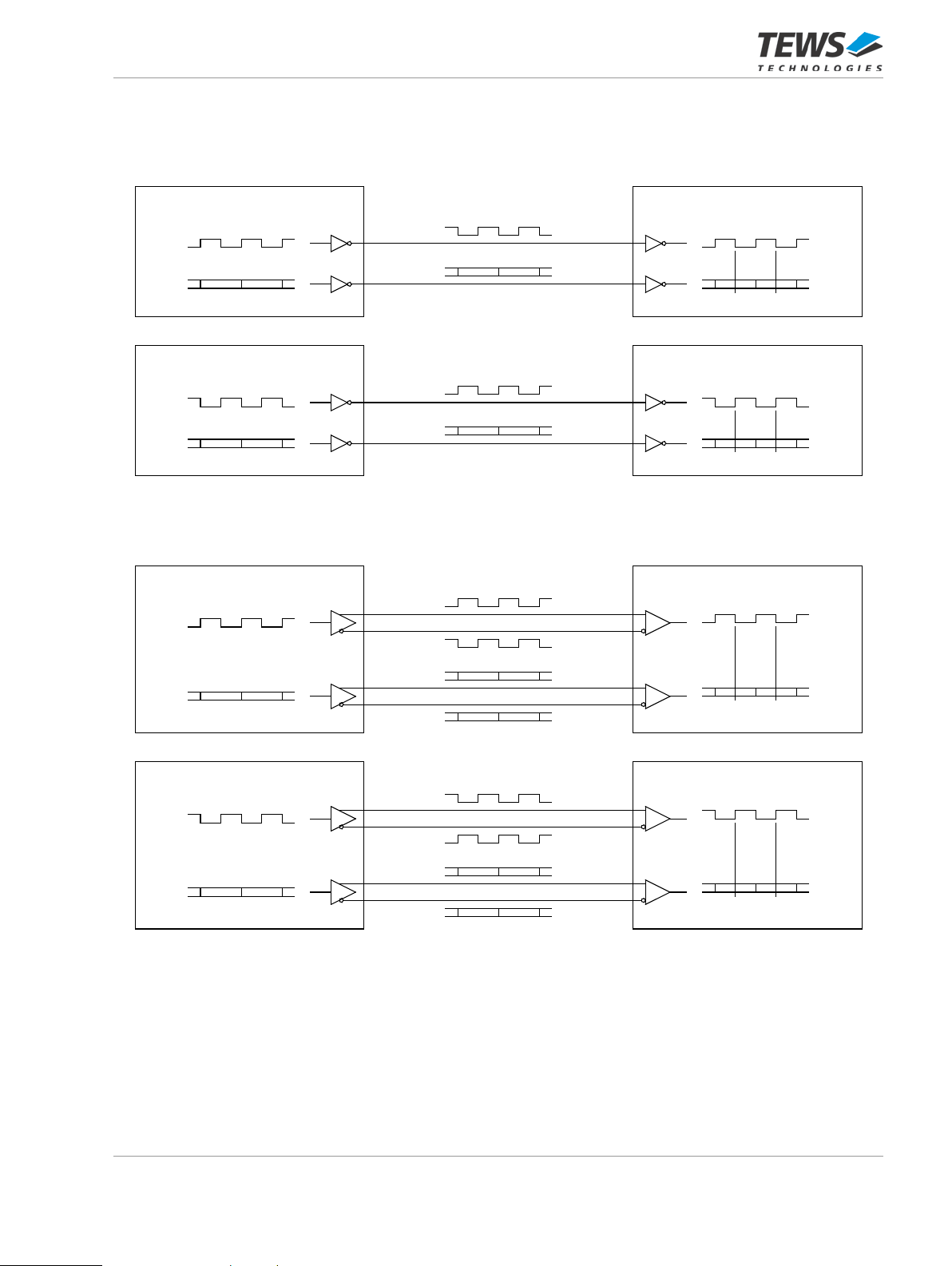
Board Level
TXC
TXD
RXC
RXD
TXCINV = 0 RXCINV = 0
TXC
TXD
RXC
RXD
TXCINV = 1
RS232 T ype Cable Interface
RS232 T ype Cable Interface
TXC
TXD
RXC
RXD
TXCINV = 0 RXCINV = 0
RS422 T ype Cable Interface
TXC
TXD
RXC
RXD
TXCINV = 1 RXCINV = 1
RS422 T ype Cable Interface
RXCINV = 1
Board Level
Board Level
Board Level
Transmit & Receive Clock Polarity 8.4
Figure 8-1 : Transmit & Receive Clock Polarity
TPCE863 User Manual Issue 1.0.1 Page 69 of 72
Page 70
9 Module Management
LED
Color
Description
On Board LEDs 9.1
For a quick visual ins pection the TPCE863 provides on board LEDs at the component side. These indicate
correct voltage supply and FPGA configuration state.
DONE Green Shows whether the FPGA has configured or not
3.3 Green PCIe Connector provided 3.3V voltage is valid
2.5 Green On board 2.5V voltage is in desired range
1.2 Green On board 1.2V voltage is in desired range
1.0 Green On board 1.0V voltage is in desired range
Table 9-1 : On Board LEDs
TPCE863 User Manual Issue 1.0.1 Page 70 of 72
Page 71
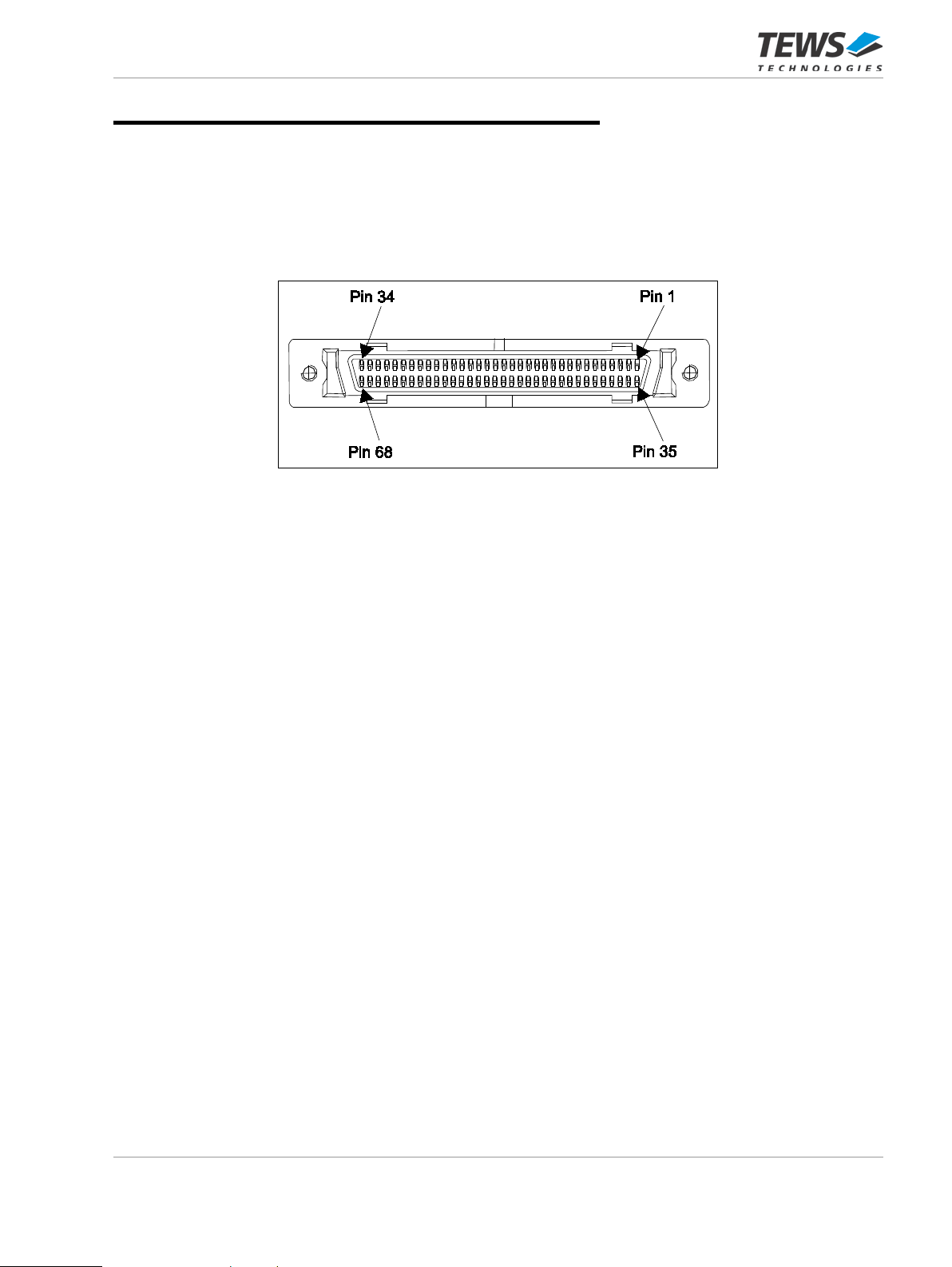
10 Pin Assignment – I/O Connector
Front Panel I/O Connector 10.1
AMP 787082-7 or compatible
Figure 10-1 : Front Panel I/O Connector Numbering
TPCE863 User Manual Issue 1.0.1 Page 71 of 72
Page 72
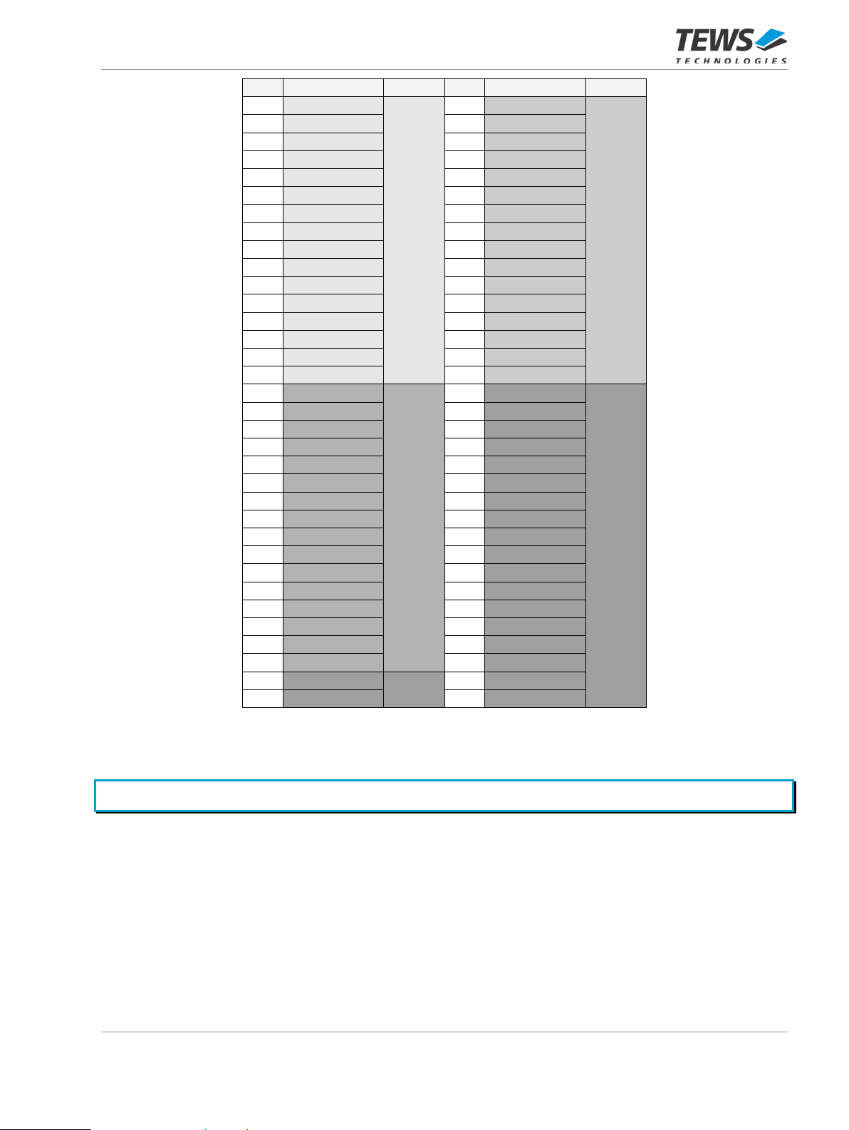
Pin
Signal
Port
Pin
Signal
Port
1
CDA/-
35
CDA/-
2
CDB/+
36
CDB/+
3
RXDA/-
37
RXDA/-
4
RTSA/-
38
RTSA/-
5
TXDA/-
39
TXDA/-
6
CTSA/-
40
CTSA/-
7
RTSB/+
41
RTSB/+
8
CTSB/+
42
CTSB/+
9
GND
43
GND
10
TXDB/+
44
TXDB/+
11
RXDB/+
45
RXDB/+
12
TXCA/-
46
TXCA/-
13
TXCB/+
47
TXCB/+
14
GND
48
GND
15
RXCA/-
49
RXCA/-
16
RXCB/+
50
RXCB/+
17
CDA/-
51
CDA/-
18
CDB/+
52
CDB/+
19
RXDA/-
53
RXDA/-
20
RTSA/-
54
RTSA/-
21
TXDA/-
55
TXDA/-
22
CTSA/-
56
CTSA/-
23
RTSB/+
57
RTSB/+
24
CTSB/+
58
CTSB/+
25
GND
59
GND
26
TXDB/+
60
TXDB/+
27
RXDB/+
61
RXDB/+
28
TXCA/-
62
TXCA/-
29
TXCB/+
63
TXCB/+
30
GND
64
GND
31
RXCA/-
65
RXCA/-
32
RXCB/+
66
RXCB/+
33
DSRB/+
67
DTRB/+
34
DSRA/-
68
DTRA/-
0
2
1
3
3
Table 10-1 : Front I/O Pin Assignment
In V.28 (single-ended) mode, only the signals ending with “A” are used.
TPCE863 User Manual Issue 1.0.1 Page 72 of 72
 Loading...