

Page 1

The Embedded I/O Company
TIP810
CAN Bus IP
Version 3.0
User Manual
Issue 3.0.4
March 2009
TEWS TECHNOLOGIES GmbH TEWS TECHNOLOGIES LLC
Am Bahnhof 7
25469 Halstenbek, Germany
www.tews.com
Phone: +49-(0)4101-4058-0
Fax: +49-(0)4101-4058-19
e-mail: [email protected]
9190 Double Diamond Parkway,
Suite 127, Reno, NV 89521, USA
www.tews.com
Phone: +1 (775) 850 5830
Fax: +1 (775) 201 0347
e-mail: [email protected]
Page 2

TIP810 Version 3.0 User Manual Issue 3.0.4 Page 2 of 19
TIP810-10
CAN Bus IP
This document contains information, which is
proprietary to TEWS TECHNOLOGIES GmbH. Any
reproduction without written permission is forbidden.
TEWS TECHNOLOGIES GmbH has made any
effort to ensure that this manual is accurate and
complete. However TEWS TECHNOLOGIES GmbH
reserves the right to change the product described
in this document at any time without notice.
TEWS TECHNOLOGIES GmbH is not liable for any
damage arising out of the application or use of the
device described herein.
Style Conventions
Hexadecimal characters are specified with prefix 0x,
i.e. 0x029E (that means hexadecimal value 029E).
For signals on hardware products, an ‚Active Low’ is
represented by the signal name with # following, i.e.
IP_RESET#.
Access terms are described as:
W Write Only
R Read Only
R/W Read/Write
R/C Read/Clear
R/S Read/Set
©2001-2009 by TEWS TECHNOLOGIES GmbH
All trademarks mentioned are property of their respective owners.
Page 3

TIP810 Version 3.0 User Manual Issue 3.0.4 Page 3 of 19
Issue Description Date
1.0 Initial Issue October 2001
1.1 Addressing description modified November 2001
1.2 Changed Block Diagram and General Revision October 2002
1.3 New address TEWS LLC September 2006
3.0.4 New notation of User Manual Issue March 2009
Page 4

TIP810 Version 3.0 User Manual Issue 3.0.4 Page 4 of 19
Table of Contents
1 PRODUCT DESCRIPTION.........................................................................................6
2 COMPATIBILITY WITH TIP810 V1.0, V2.0................................................................7
3 TECHNICAL SPECIFICATION...................................................................................8
4 ID PROM CONTENTS................................................................................................ 9
5 TIP810 ADDRESSING.............................................................................................. 11
5.1 "BasiCAN" Mode Register Set.....................................................................................................12
5.2 "PeliCAN"-Mode Register Set......................................................................................................13
5.3 Interrupt Vector Register..............................................................................................................15
6 PROGRAMMING......................................................................................................16
6.1 Initialization of the Hardware.......................................................................................................16
6.2 Programming of the SJA1000 Controller....................................................................................16
7 INSTALLATION........................................................................................................17
7.1 Configuration of the TIP810.........................................................................................................17
7.2 Bus Line Termination ...................................................................................................................17
8 PIN ASSIGNMENT...................................................................................................18
8.1 Pin Assignment of 50 pin I/O flat cable.......................................................................................18
8.1.1 CAN High Speed (Pin 01 - 18) TIP810..............................................................................18
8.1.2 CAN with modified RS485 (Pin 33 – 50) TIP810...............................................................19
Page 5

TIP810 Version 3.0 User Manual Issue 3.0.4 Page 5 of 19
List of Figures
FIGURE 1-1: BLOCK DIAGRAM TIP810..........................................................................................................6
FIGURE 5-1: INTERRUPT VECTOR REGISTER INTVEC............................................................................15
FIGURE 7-1: JUMPER CONFIGURATION.....................................................................................................17
List of Tables
TABLE 3-1 : TECHNICAL SPECIFICATION TIP810........................................................................................8
TABLE 4-1 : ID PROM CONTENTS TIP810 V1.0.............................................................................................9
TABLE 4-2 : ID PROM CONTENTS TIP810 V2.0.............................................................................................9
TABLE 4-3 : ID PROM CONTENTS TIP810 V3.0...........................................................................................10
TABLE 5-1 : "BASICAN" MODE REGISTER SET..........................................................................................12
TABLE 5-2 : "PELICAN"-MODE REGISTER SET ..........................................................................................14
TABLE 8-1 : PIN ASSIGNMENT FOR CAN HIGH SPEED ............................................................................18
TABLE 8-2 : PIN ASSIGNMENT FOR CAN MOD. RS485.............................................................................19
Page 6
TIP810 Version 3.0 User Manual Issue 3.0.4 Page 6 of 19
1 Product Description
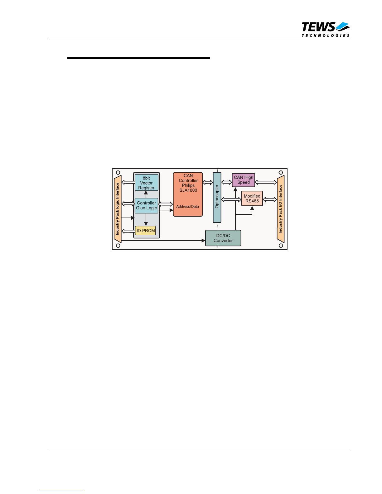
The TIP810 is an IndustryPack® compatible module with a complete CAN bus interface using the
Philips SJA1000 CAN controller. The Philips SJA1000 CAN controller is a stand-alone controller for
the Controller Area Network (CAN) used within automotive and general industrial environments.
It is the successor of the PCA82C200 CAN controller (Basic CAN) from Philips Semiconductors which
was used on the TIP810-10 V1.0. Additionally, a new mode of operation (PeliCAN) is implemented on
the SJA1000 which supports the CAN 2.0B protocol specification with several new features. The
SJA1000 has the capability to transmit, receive and perform message filtering on standard and
extended messages.
The TIP810 supports a 8 bit bus interface which permits byte accesses to the internal registers of the
SJA1000 controller. The physical interface supports both, CAN high-speed (according to ISO11898)
and modified RS485. Both physical interfaces are optically isolated from the CAN controller. An on
board DC/DC converter supplies the isolated parts of the TIP810.
Figure 1-1: Block Diagram TIP810
Page 7

TIP810 Version 3.0 User Manual Issue 3.0.4 Page 7 of 19
2 Compatibility with TIP810 V1.0, V2.0
The TIP810 V3.0 uses the SJA1000 CAN controller as a replacement of the PCA82C200 CAN
controller which was used on the TIP810 V1.0. The TIP810 V2.0 also had used the SJA1000 CAN
controller, but only in a PCA82C200 compatible way.
The SJA1000 CAN controller on the TIP810 is register-, pin- and function-compatible with the
PCA82C200 if operating in the “BasiCAN" Mode. This mode is the default mode for the SJA1000
CAN controller after power-on.
In the “PeliCAN" Mode the SJA1000 CAN controller supports the full CAN2.0B protocol specification
plus additional features.
Setting the SJA1000 Operation Mode:
The modes can be switched via bit 7 in the Clock Divider Register if the controller is in reset mode.
For a detailed description of the SJA1000 CAN controller, it’s operating modes and additional features
please refer to the SJA1000 data sheet, which is part of the TIP810-ED V3.0 engineering
documentation.
Page 8
TIP810 Version 3.0 User Manual Issue 3.0.4 Page 8 of 19
3 Technical Specification
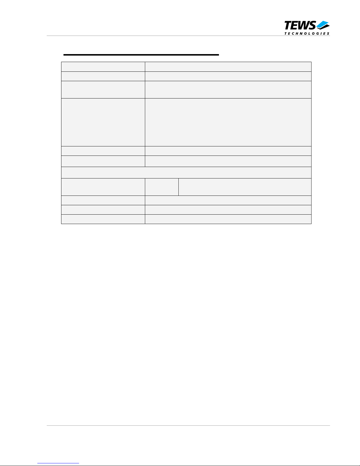
Interface
Single Size IndustryPack® Logic Interface
CAN Controller
Philips SJA 1000
Physical Interface
CAN High Speed (according to ISO11898)
Modified RS485
Wait States
IDSEL#: No wait state
IOSEL#: No wait state (read/write acce ss to the vector
register)
1 wait state (read/write access to the SJA1000)
INTSEL#: No wait state
MEMSEL#: 1 wait state (read/write access to the SJA1000)
Interface
50-conductor flat cable
Power Requirements
220mA typical @ +5V DC
Physical Data
Temperature Range
Operating
Storage
-40° C to +85 °C
-55°C to +125°C
MTBF
362160 h
Humidity
5 – 95 % non-condensing
Weight
27 g
Table 3-1 : Technical Specification TIP810
Page 9
TIP810 Version 3.0 User Manual Issue 3.0.4 Page 9 of 19
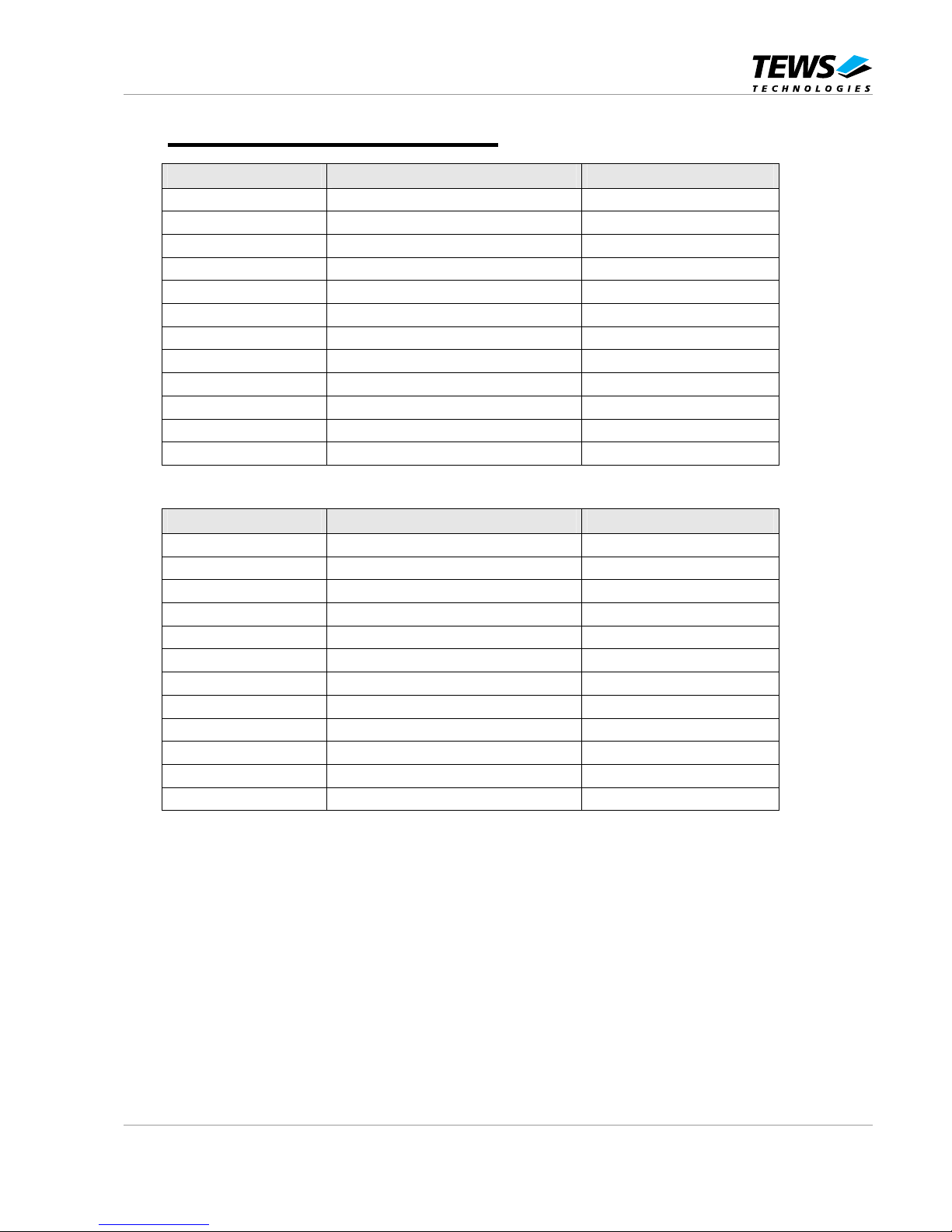
4 ID PROM Content s
Address Function Contents
0x01
ASCII ‘I’
0x49
0x03
ASCII ‘P’
0x50
0x05
ASCII ‘A’
0x41
0x07
ASCII ‘C’
0x43
0x09
Manufacturer ID
0xB3
0x0B
Model Number
0x01
0x0C
Revision
0x10
0x0F
Reserved
0x00
0x11
Driver-ID Low - Byte
0x00
0x13
Driver-ID High - Byte
0x00
0x15
Number of bytes used
0x0C
0x17
CRC
0x11
Table 4-1 : ID PROM Contents TIP810 V1.0
Address Function Contents
0x01
ASCII ‘I’
0x49
0x03
ASCII ‘P’
0x50
0x05
ASCII ‘A’
0x41
0x07
ASCII ‘C’
0x43
0x09
Manufacturer ID
0xB3
0x0B
Model Number
0x01
0x0C
Revision
0x20
0x0F
Reserved
0x00
0x11
Driver-ID Low - Byte
0x00
0x13
Driver-ID High - Byte
0x00
0x15
Number of bytes used
0x0C
0x17
CRC
0x9D
Table 4-2 : ID PROM Contents TIP810 V2.0
Page 10

TIP810 Version 3.0 User Manual Issue 3.0.4 Page 10 of 19
Address Function Contents
0x01
ASCII ‘I’
0x49
0x03
ASCII ‘P’
0x50
0x05
ASCII ‘A’
0x41
0x07
ASCII ‘C’
0x43
0x09
Manufacturer ID
0xB3
0x0B
Model Number
0x01
0x0C
Revision
0x30
0x0F
Reserved
0x00
0x11
Driver-ID Low - Byte
0x00
0x13
Driver-ID High - Byte
0x00
0x15
Number of bytes used
0x0C
0x17
CRC
0x19
Table 4-3 : ID PROM Contents TIP810 V3.0
Page 11

TIP810 Version 3.0 User Manual Issue 3.0.4 Page 11 of 19
5 TIP810 Addressing
TIP810 Address range:
SJA1000 CAN Controller Register Set:
ip_io_base_address + (0x01 to 0x3F) (lower 32byte register space)
ip_mem_base_address + (0x01 to 0xFF) (complete register space)
Interrupt Vector Register INTVEC:
ip_io_base_address + (0x41)
Page 12

TIP810 Version 3.0 User Manual Issue 3.0.4 Page 12 of 19
5.1 "BasiCAN" Mode Register Set
The lower 32bytes of the SJA1000 register space (address offset 0x01 – 0x3F) are accessible in the
IP I/O Space. This covers the complete "BasiCAN" mode register set.
All registers are byte sized. Read accesses to write-only registers will result in a value of 0xFF on the
data bus.
Register (function in Operating/Reset Mode) Address Access
Control Register (control/control) 0x01 R/W
Command Register 0x03 W
Status Register (status/status) 0x05 R
Interrupt Register (interrupt/interrupt) 0x07 R
Acceptance Code Register (0xFF/acceptance code) 0x09 R/(W)
Acceptance Mask Register (0xFF/acceptance mask) 0x0B R/(W)
Bus Timing Register 0 (0xFF/Bus Timing 0) 0x0D R/(W)
Bus Timing Register 1(0xFF/Bus Timing 1) 0x0F R/(W)
Output Control Register (0xFF/Output Control) 0x11 R/(W)
Test Register 0x13 R
Transmit Buffer Identifier (identifier 10 to 3/0xFF 0x15 R/W
Transmit Buffer RTR, Data length (identifier 2 to 0/0xFF) 0x17 R/W
Transmit Buffer Byte 1 (data byte 1/0xFF) 0x19 R/[W]
Transmit Buffer Byte 2 (data byte 2/0xFF) 0x1B R/[W]
Transmit Buffer Byte 3 (data byte 3/0xFF) 0x1D R/[W]
Transmit Buffer Byte 4 (data byte 4/0xFF) 0x1F R/[W]
Transmit Buffer Byte 5 (data byte 5/0xFF) 0x21 R/[W]
Transmit Buffer Byte 6 (data byte 6/0xFF) 0x23 R/[W]
Transmit Buffer Byte 7 (data byte 7/0xFF) 0x25 R/[W]
Transmit Buffer Byte 8 (data byte 8/0xFF) 0x27 R/[W]
Receive Buffer Identifier (identifier 10 to 3/identifier 10 to 3) 0x29 R/W
Receive Buffer RTR, Data length (identifier 2 to 0/identifier 2 to 0) 0x2B R/W
Receive Buffer Byte 1 (data byte 1/data byte 1) 0x2D R/W
Receive Buffer Byte 2 (data byte 2/data byte 2) 0x2F R/W
Receive Buffer Byte 3 (data byte 3/data byte 3) 0x31 R/W
Receive Buffer Byte 4 (data byte 4/data byte 4) 0x33 R/W
Receive Buffer Byte 5 (data byte 5/data byte 5) 0x35 R/W
Receive Buffer Byte 6 (data byte 6/data byte 6) 0x37 R/W
Receive Buffer Byte 7 (data byte 7/data byte 7) 0x39 R/W
Receive Buffer Byte 8 (data byte 8/data byte 8) 0x3B R/W
Reserved (0xFF/0xFF) 0x3D R
Clock Divider Register 0x3F R/W
Table 5-1 : "BasiCAN" Mode Register Set
Page 13

TIP810 Version 3.0 User Manual Issue 3.0.4 Page 13 of 19
5.2 "PeliCAN"-Mode Register Set
The complete SJA1000 “PeliCAN" mode register set is accessible in the IP Memory Space. (Only the
lower 32bytes of the "PeliCAN"-Mode register set are accessible in IP I/O Space.) All registers are
byte sized. Read accesses to write-only registers will result in a value of 0xFF on the data bus.
Register (function in Operating/Reset Mode) Address Access
Mode Register (mode/mode) 0x01 R/W
Command Register 0x03 W
Status Register (status/status) 0x05 R
Interrupt Register (interrupt/interrupt) 0x07 R
Interrupt Enable Register (interrupt enable/interrupt enable) 0x09 R/W
Reserved (0x00/0x00) 0x0B R
Bus Timing Register 0 (Bus Timing 0/Bus Timing 0) 0x0D R/(W)
Bus Timing Register 1(Bus Timing 1/Bus Timing 1) 0x0F R/(W)
Output Control Register (Output Control /Output Control) 0x11 R/(W)
Test Register 0x13 R
Reserved (0x00/0x00) 0x15 R
Arbitration Lost Capture Register (ALC/ALC) 0x17 R
Error Code Capture Register (ECC/ECC) 0x19 R
Error Warning Limit Register (EWL/EWL) 0x1B R/(W)
RX Error Counter Register (RX Error Counter/RX Error Counter) 0x1D R/(W)
TX Error Counter Register (TX Error Counter/TX Error Counter) 0x1F R/(W)
TX,RX Frame information Register (TX,RX Frame information/
Acceptance Code)
0x21 R/W
TX,RX Identifier 1 Register (TX,RX Identifier 1/Acceptance Code 1) 0x23 R/W
TX,RX Identifier 2 Register (TX,RX Identifier 2/Acceptance Code 2) 0x25 R/W
TX,RX Identifier 3 Register (TX,RX Identifier 3/Acceptance Code 3) 0x27 R/W
TX,RX Identifier 4 Register (TX,RX Identifier 3/Acceptance Mask 0) 0x29 R/W
TX, RX Data 1 Register /Acceptance Mask 1 0x2B R/W
TX, RX Data 2 Register /Acceptance Mask 2 0x2D R/W
TX, RX Data 3 Register /Acceptance Mask 3 0x2F R/W
TX, RX Data 4 Register /0x00 0x31 R/W
TX, RX Data 5 Register /0x00 0x33 R/W
TX, RX Data 6 Register /0x00 0x35 R/W
TX, RX Data 7 Register /0x00 0x37 R/W
TX, RX Data 8 Register /0x00 0x39 R/W
RX Message Counter Register (RX Message Counter/ RX Message
Counter)
0x3B R
RX Buffer Start Address Register (RX Buffer Start Address/ RX Buffer
Start Address)
0x3D R/W
Clock Divider Register (Clock Divider/ Clock Divider) 0x3F R/W
Internal RAM address 0 (FIFO) 0x41 R/W
Internal RAM address 1 (FIFO) 0x43 R/W
Internal RAM address 2 (FIFO) 0x45 R/W
Page 14
TIP810 Version 3.0 User Manual Issue 3.0.4 Page 14 of 19
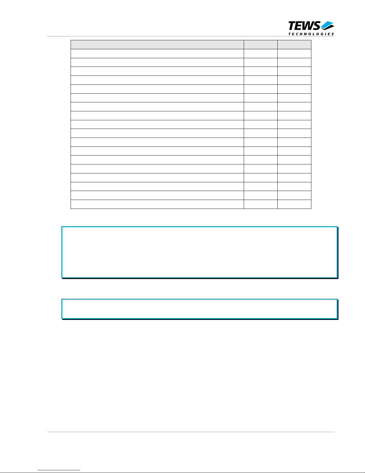
Register (function in Operating/Reset Mode) Address Access
. . .
. . .
. . .
Internal RAM address 63 (FIFO) 0xBF R/W
Internal RAM address 64 (TX buffer) 0xC1 R/W
. . .
. . .
. . .
Internal RAM address 76 (TX buffer) 0xD9 R/W
Internal RAM address 77 (free) 0xDA R/W
Internal RAM address 78 (free) 0xDB R/W
Internal RAM address 79 (free) 0xDC R/W
0x00 0xDD R
0x00 0xDE R
. . .
. . .
. . .
0x00 0xFF R
Table 5-2 : "PeliCAN"-Mode Register Set
R/(W) : These Registers can only be written in Reset Mode!
R/[W] : These Register can only be written in Operating Mode!
R : Read only
W : Write only
When operating in "PeliCAN"-Mode the Interrupt Vector Register is still mapped to address
offset 0x41 in the IP I/O Space.
Page 15
TIP810 Version 3.0 User Manual Issue 3.0.4 Page 15 of 19
5.3 Interrupt Vector Register
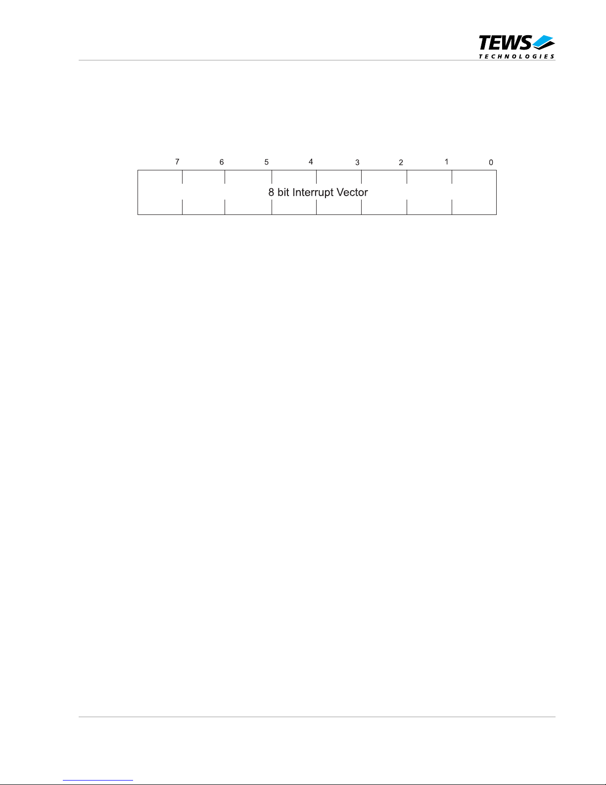
The Interrupt Vector Register INTVEC of the TIP810 is a byte wide read/write register located at
address ip_io_base_address + (0x41).
Figure 5-1: Interrupt Vector Register INTVEC
The 8-bit interrupt vector must be loaded by software during initialization of the TIP810.
The Philips SJA1000 CAN controller can generate interrupts on interrupt request line INTREQ0/ of the
IP bus.
Detailed Interrupt Status information can be obtained by read accesses to the Interrupt Register of the
SJA1000 at offset 0x07. Read accesses will reset all interrupt status bits except for the receive
interrupt bit.
Each single interrupt source of the SJA1000 CAN controller can be enabled/disabled in the Interrupt
Enable Register of the SJA1000 at offset 0x09.
Page 16

TIP810 Version 3.0 User Manual Issue 3.0.4 Page 16 of 19
6 Programming
6.1 Initialization of the Hardware
The Output Control Register of the Philips SJA1000 CAN controller must be programmed for the two
physical interfaces.
Set the SJA1000 Output Control Register (Offset 0x11) to value 0xDA for CAN High Speed and
Modified RS485.
6.2 Programming of the SJA1000 Controller
For programming the SJA1000 CAN controller please refer to the SJA1000 data sheet, which is part of
the TIP810-ED engineering documentation.
Page 17
TIP810 Version 3.0 User Manual Issue 3.0.4 Page 17 of 19
7 Installation
7.1 Configuration of the TIP810
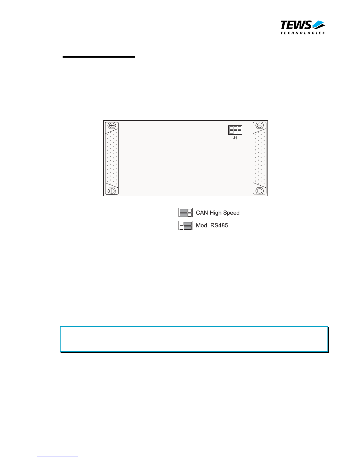
The TIP810 must be configured by the jumper field J1 for the desired physical interface:
CAN High Speed Jumper 1 – 3 and 2 – 4 installed.
mod. RS485 Jumper 3 – 5 and 4 – 6 installed.
Figure 7-1: Jumper Configuration
7.2 Bus Line Termination
To reduce the stub length of the TIP810 to a minimum, the CAN bus lines for high speed and for mod.
RS485 are connected twice to the IP I/O connector. This means that the CAN bus is routed through
the TIP810.
No termination is provided on board of the TIP810. If the TIP810 is located at one extreme end of the
CAN bus lines then external termination must be provided.
The CAN bus lines must be terminated at both extreme ends of the cable with a resistor,
connected between both CAN bus lines (CAN_H and CAN_L). Resistor value should be equal to
the impedance of the twisted pair (typical 120 ohms).
Page 18
TIP810 Version 3.0 User Manual Issue 3.0.4 Page 18 of 19
8 Pin Assignment
8.1 Pin Assignment of 50 pin I/O flat cable
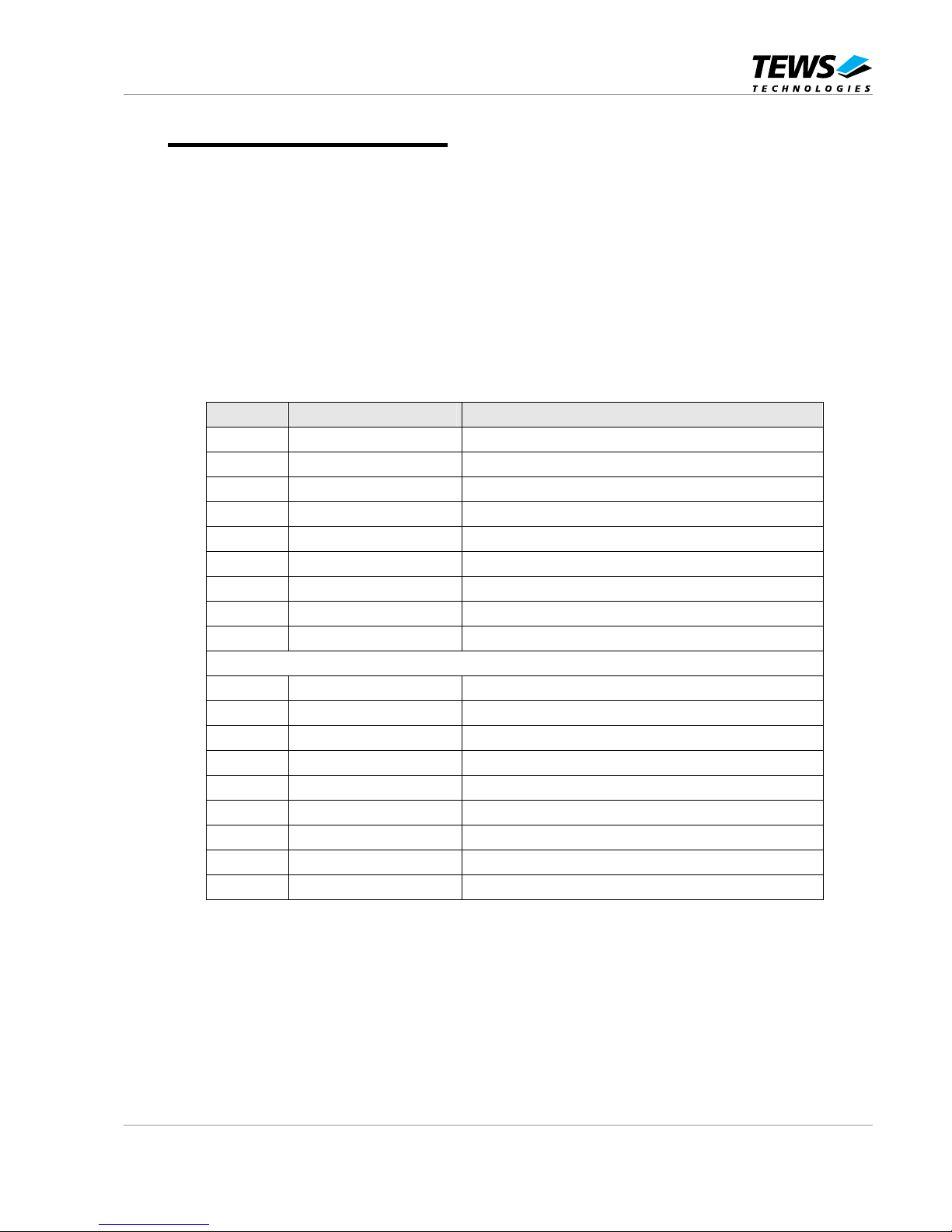
The 50-pin flat cable from the IP carrier board will be split into four 9-pin sections. Two sections of the
50 pin flat cable are routed to the CAN High Speed driver and the other two sections are routed to the
modified RS485 driver.
8.1.1 CAN High Speed (Pin 01 - 18) TIP810
The line 1 – 9 fit directly to a 9 pin SUB-D male connector. The assignment of the 9 pin SUB-D
connector meets the suggestion of the CiA (CAN in Automation). Line 1 – 9 is connected on board
with line 10 – 18. With this it is very easy to connect the TIP810 to the CAN bus.
I/O Line 9 pin SUB-D Description according to CIA
1 1 Reserved
2 6 (GND, Optional Input Ground)
3 2 CAN_L bus line CAN High Speed
4 7 CAN_H bus line CAN High Speed
5 3 GND (Ground)
6 8 Reserved (Error line)
7 4 Reserved
8 9 (V+, Optional Input Power)
9 5 Reserved
++++++++++++++++++++++++++++++++++++++++++++++++++++++++++++++++++
10 1 Reserved
11 6 (GND, Optional Input Ground)
12 2 CAN_L bus line CAN High Speed
13 7 CAN_H bus line CAN High Speed
14 3 GND Ground
15 8 Reserved
16 4 Reserved
17 9 (V+, Optional Input Power)
18 5 Reserved
Table 8-1 : Pin Assignment for CAN High Speed
Page 19
TIP810 Version 3.0 User Manual Issue 3.0.4 Page 19 of 19
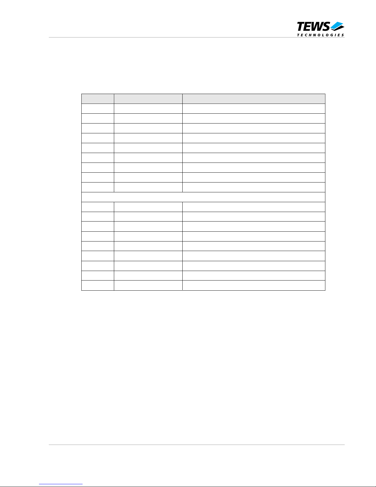
8.1.2 CAN with modified RS485 (Pin 33 – 50) TIP810
The line 42 – 50 fit directly to a 9 pin SUB-D male connector. The assignment of the 9 pin SUB-D
connector meets the suggestion of the CiA (CAN in Automation). Lines 42 – 50 are connected on
board with line 33 – 41. With this it is very easy to connect the TIP810 to the CAN bus.
I/O Line 9 pin SUB-D Description according to CIA
33 1 Reserved
34 6 (GND, Optional Input Ground)
35 2 CAN_L bus line RS485
36 7 CAN_H bus line RS485
37 3 GND (Ground)
38 8 Reserved (Error line)
39 4 Reserved
40 9 (V+, Optional Input Power)
41 5 Reserved
++++++++++++++++++++++++++++++++++++++++++++++++++++++++++++++++++
42 1 Reserved
43 6 (GND, Optional Input Ground)
44 2 CAN_L bus line RS485
45 7 CAN_H bus line RS485
46 3 GND (Ground)
47 8 Reserved (Error line)
48 4 Reserved
49 9 (V+, Optional Input Power)
50 6 Reserved
Table 8-2 : Pin Assignment for CAN Mod. RS485
 Loading...