

Page 1

-)
TELEX
Service
Manual
PROFESSIONAL
WIRELESS
INTERCOM SYSTEM
TR-200
SERIES
TELEX,
Page 2

Table of Contents
Page
CHAPTER 1- GENERAL INEORMATION 1-1
GENERAL DESCRIPTION
SPECIFICATIONS TR-200
CONTROLS
External Controls
Internal Controls
CHAPTER 2
GENERAL
CHAPTER 3 . TRANSMIT AND
TR-200 INSTRUMENT DISASSEMBLY
TRANSMIT BOARD
CIRCUIT DESCRIPTION
ALIGNMNENT PROCEDURE
VOLTAGE TABLES
RECEIVE BOARD
CIRCUIT DESCRIPTION
ALIGNMENT PROCEDURE 3-5
OPTIONS - CIRCUIT DESCRIPITION 3-5
I
'
\
!
VOLTAGE TABLES
ELECTRICAL PARTS RECEIVE PCB ASSEMBLY (879977-*)
ELECTRICAL PARTS TRANSMIT PCB ASSEMBLY (879976-*)
AND
CONNECTIONS
.............................................................................................................................
..............................................................................................................................
.
IDENTIFICATION OF CIRCUIT BOARD VERSION
...........................................................................................................................................
..............................................................................................................................
................................................................................................................
.................................................................................................................
RECEI~
..........................................................................................................................
...............................................................................................................
................................................................
-
TRANSMIT BOARD
..............................................................................................................
.........................................................................................................
-
RECEIVE BOARD
...........................................................................................
..................................................................................................
.................................................
~
.
~-~~
CIRCUIT BOARDS
.......................................................
..........................................................................................
...................................
,
.................................................................................
.........................................................................................
....................................................................................
................................................
................................................
...
1-1
1-2
1-3
1-3
1-4
2-1
2-1
3-1
3-1
3-3
3-3
3-3
3-4
3-5
3-5
3-6
3-15
3-17
Page 3
Figure
1-1
1-2
1-3
2- 1
3- 1
3-2
List
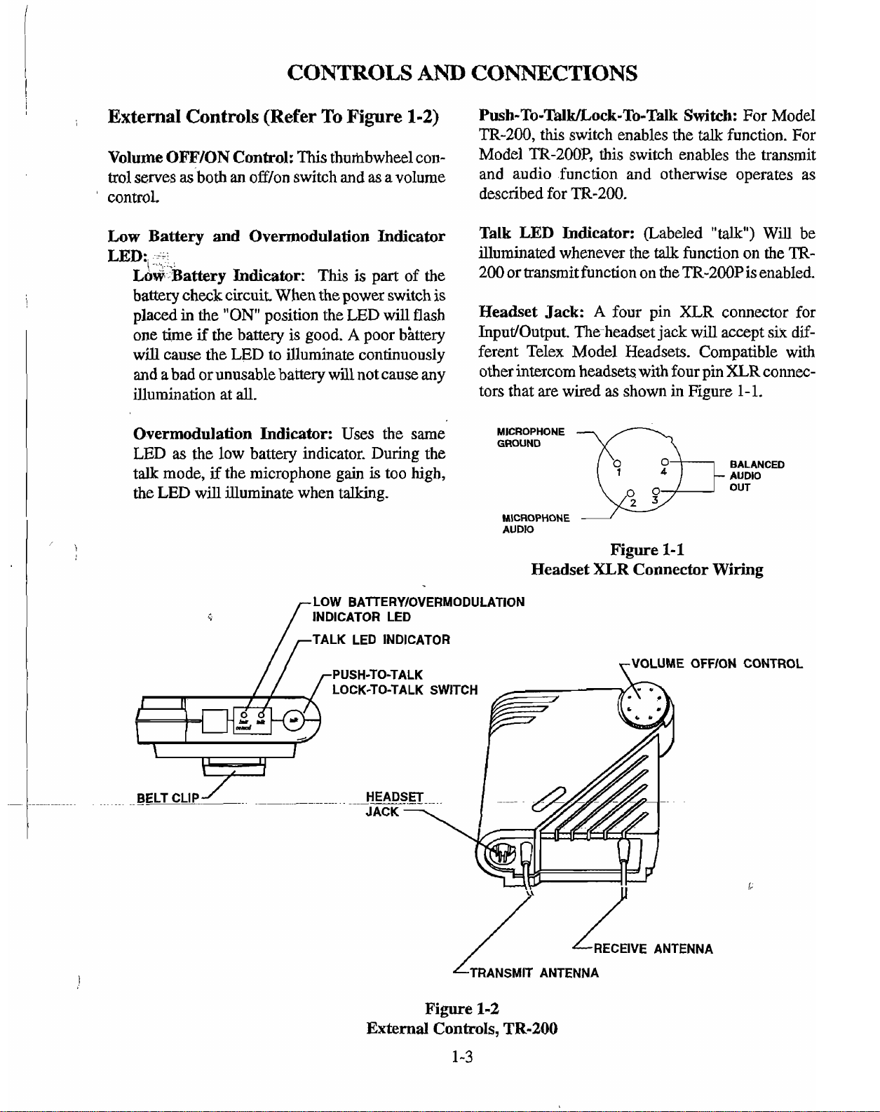
Headset XLR Connector Wiring
External Controls, TR-200
Internal Controls, TR-200
Version Flow Chart
Exploded View
P.C.
Board Assembly - Receiver (879977-) Component Layout
(Component Side)
P.C.
Board Assembly - Transmit (879976-) Component Layout
(Component Side)
Transmit P.C. Board Assembly Component Layout (Foil Side View)
Receive
Schemat~c Diagram TR-200 Version 4
Schematic Diagram TR-2M) Version 3
Schematic Diagram TR-200 Version
Schematic Diagram TR-200 Version 1
P.C.
.
of
TR-200 3-2
Board Assembly Component Layout (Foil Side View)
.
of
Illustrations
..............................................................................
..................................................................................
........................................................................................
..................................................................................................
.......................................................................................
..............................................................................................
................................................................................................
..................................................................
..................................................................
2
..................................................................
.................................
1
............................
...................
....................
Page
1-3
1-3
1-9
2-1
3-9
3-9
3-10
3-10
3-11
3-12
3-13
3-14
.
1
Page 4

CHAPTER
1
GENERAL INFORMATION
GENERAL
The Telex Models TR-200 and TR-200P Belt-pack
Transceivers
one receive channel.
The TR-200 is a portable unit which communicates
in
full duplex with either the BTR-200 base station
or a mirror image TR-200.
Push-to-Talk with Lock-to-TaLk feature switch for
the TR-200 and Push-to-Transmit
Transmit feature for the TR-200P.
DESCRIPTION
are
designed with one transmit and
with
Lock-to-
The TR-200
transmit mode with the audio, to
a switch. As many as four TR-200 belt-pack
transceivers can operate in a fully duplex network
with
one Telex Model BTR-200 or BTR-200
Base Station.
The TR-200P Transceiver operates in the Push-to-
transmit mode (the transmit and talk function
activated together). Any number of TR-200P
transceivers can be used
with one BTR-200 or BTR-200
Operate only one transmitter at a time. Attempting
to use two transmitters simultaneously on the same
channel
Transceiver operates
will
cause interference.
in
the continuous
talk,
activated by
in
a half-duplex network
11
Base Station.
II
are
Page 5

SPECIFICATIONS
Power Requirements
Current Drain
Temperature Range
Dimensions
Weight
Transmit Antenna
Receive Antenna
RF
RF
RF
Modulation
Modulation Limter
Modulation Frequency Range
Microphone Audio Input
Microphone Input Sensluvlty
Radiated Harmonics and Spurious Emissions
FCC
........................................................................................................
Frequency Range
Frequency Stability
Power Output
.......................................................................................
................................................................................................................
...........................................................................................
.........................................................
.
.........................................................
.............................................................................
.........................................................................................
..........................................................................................
.....................................................................................................
............................................................................
........................................................................................................
~.
.
.............................................................................................
...........................................................................
...........................................................................................
...
..............................................................
.
.
TR-200
Overall
6
AA
cells (Alkaline,
Nickel Cadmium Optional
4
to 130'~ (-20'~ to 55'~)
4.25" W x 4.125" H x 2.0" D
(108mm
1302 (369g) with batteries
114-wave wire (attached)
114-wave wire (attached)
Transmit
C Controlled, 0.005%
..........................................
115 micro-seconds Pre-emphasis
2 mV Dynamic, 4 mV Electret
.......................................................................
Type Accepted Under Parts 90 and 74
FM,
Exceeds FCC Specifications
NEDA,
x
105mm x 51mm)
5000
Internal Compressor
300
to 5000 Hz =dB
30 to 3500 ohms
MN
1500)
typ c 65
150-216 MHz
50 mW Typical
Hz
mA
deviation,
-45 dBC,
-
cp-~~~~
I
%
Receive
RF
Frequency Range
RF
Frequency Stabiltiy
RF
IF
Image
Squelch Quietmg
Squelch Threshold
~
Signal:io-No~se Raao 90 dB
Audio Output
Distortion
FCC
...
Sensihvity
Selectivity
Rejection
..............................................................................
.....................................................................................
. .
.
.
..................................................................................
.............................................................................................
..........................................................................................................
.....................................................................................................
....................................................................
Dual Conversion Superheterodyne,
st Controlled, O.QOS%Type
Less than 0.5 pV for 12 dB SINAB
3 dB at 30 kHz (Ceramic Filter)
..........................................................................................................
........................................................................................................................
......................................................................................................
.
~
~~~-
~~
~~~~~~~
-
--
.................................................................................................................
32 mW into
Less than 1% at Rated Output
Notification Under
150-216 MHz
70 dB or better
1.OpV (Internal)
~~
~
600
ohms (Headset)
FM
90 dB
Part
15
Page 6
I
I
CONTROLS
AND
CONNECTIONS
External
Volume OFJ?/ON Control:
trol serves
control. described for
Low Battery and Overmodulation Indicator
LED:,
Low Battery Indicator:
battery check circuit. When the power switch is
placed in the
one time
will cause the
and
illumination at
Overmodulation Indicator:
LED
talk mode,
the
Controls (Refer To Figure
This thumbwheel con-
as
both
an
off/on switch and
This
is
"ON"
position the
if
the battery is good. A poor bkttery
LED
to illuminate continuously
a
bad or unusable battery will not cause any
all.
as
the low battery indicator.
if
the microphone gain
LED
will illuminate when talking.
LED
Uses the same
1-2)
as
a volume
part of the
will flash
During
is
too high,
the
Push-To-Talknock-To-Talk
TR-200,
Model
and audio function and otherwise operates as
Talk LED Indicator:
illuminated whenever the
200
Headset Jack: A four pin
1nput.Output.
ferent Telex Model Headsets. Compatible with
other intercom headsets with four pin
tors that are wired
MICROPHONE
GROUND
this switch enables the
TR-200J?,
or transmit function on the
WCROPHONE
AUDIO
Switch:
talk
this switch enables the transmit
TR-200.
cabeled
talk
function on the
TR-2DOP
XLR
The headset jack will accept six dif-
as
shown in Figure 1-1.
02
9
D
Figure
1-1
For Model
function. For
"talk")
Will be
is enabled.
connector for
XLR
connec-
AUDIO
OUT
BALANCED
TR-
&&
BELTCLI
Headset
LOW BATTERYIOVERMODULATION
i
l..
d
--
INDICATOR LED
rTALK LED INDICATOR
f
USH-TO-TALK OFFION
LOCK-TO-TALK SWITCH
/
HEADSET
~~~.
/
XLR
Connector Wiring
.
"
n
RECEIVE ANTENNA
1
CONTROL
External
Figure
Controls,
1-3
1-2
TR-200
Page 7

DYNAMICIELECTRET MICROPHONE
BATTERY COMPARTMENT
GAIN CONTROL
Internal Controls
(Refer
To
Internal
Figure
Figure
Controls,
1-3)
1-3
TR-200
D~amiclElectret
Switch:
This
switch allows
selection of "D" when using a Dynamic
E"
Belt
Clip:
Combination Belt CliplSattery Cover.
Access to Battery Compartment, Microphone
Gain
Microphone or"
Microphone.
when using an Electret
Control and DynamicIElectret Switch is ac-
complished by removal of belt clip via a quick
-
release 114
lvlicrophone
-
turn
Gain
fastener.
-
-
Control:
-
-
Screwdriver adjus-
table by removing belt clip and prying out the smd
rubber plug
to
the right of the screw boss.
NOTE:
intercom are dynamic microphones. Unit is
shipped* the*" position.
Battery Compartment:
removable battery holder.
All
Telex headsets that are used with this
Holds
6
AA
batteries in a
Page 8

CHAPTER
2
IDENTIFICATION OF CIRCUIT BOARD
GENERAL
Version 1 units may be identified by the absence of
two 1.2
board assembly to the headset connector. Versions
2,
following the
later versions, the one
board)
this part is
board) wilI be a wire jumper or zero ohm resistor.
This part is
pH
chokes in the cable connecting
3,
and 4 have two such chokes immediately
P.C.
board connector.
in
is
4.7
0.1
47
pF
is
version
pE
On version 4 only
K
on
all
earlier versions.
which
2.
C45
On
versions 3 and
Of
R45
the
the three
(transmit
(trpsmit
P.C.
4
VERSION
TWO 1
-2pH
CHOKES YES OF 0.1pF
IN
LINE
h0
VALUE VALUE
.
c45
TRANMIT
BOARD BOARD
4.7pF
VERSION
2
Figure
Version
Flow
2-1
Ch-irt
OF
R45
TRANSMIT
JUMPER
VERSION 4
2-112-2
Blank
Page 9

CHAPTER
3
i
I
TRANSMIT
TR-200 INSTRUMENT
DISASSEMBLY
1.
Remove battery door and remove batteries. case.
2.
Remove 3 each
screws from the back of the unit
3.
Turn
the
TR-200
half.
NOTE:
When refitting the case front the volume
control knob must be positioned
#4
and 1 each
overand remove the front case
AND
#2
so
that the pins and
RECEIVE CIRCUIT
socket head
4.
Unplug the battery and audio cables from the
P.C.
board assembly.
5.
Lift the
6.
Unsolder the transmit and receive antenna
wires and remove the connector assembly.
7.
Unsolder shield tabs
board and
separate transmit and receive boards.
8.
Reassembly
slots mate properly. dures.
Mechanical
Parts
BOARDS
P.C.
board assembly clear of the rear
(3
places on transmit
3
places on receive board) and
is
the reverse of ihe above proce-
Receive ( 879977-*)
Transmit
Item No.
1
I
16
I
17
1
18
1
19 Terminal
I
EI
Description
Membrane Plate
Volume Knob
Transmit PCB Assembly
Stub, li4 Turn
Retainer
Cap Screw,
Cap Screw,
Case-L*bel
Retainer
Strain Relief
Receive PCB Assembly
Battery Clip
L.E.D.R~~
Choke, 1.2 uH
.
Audio Coax
Ground Shield
(879976-*)
#4
-
40 x 3/8", slotted
#2
-
56
x
5/8",
.
slotted
~---~
Part
Item
No.
22
23
24
25
26
27
~
~
28
-29-
30
3
1
32
33
34
35
36
37
38
39
40
41
42
Description
Sprocket
#2
-
56 x 1
'Screw,
L.
E.
D.,
Green
IDS
connector, 4 pin
IDS Cable Assembly
Wue Harness Assembly
FCC LBbel
BattevP-ackGushion
Battery Clip Cushion
Insulator Shield
Foam Strip
Board spacer, biva
Board Spacer
Nylon Snap Rivet, Black
Case, Front Assembly
Case, Back Assembly
Telex Label
Keypad
Connector Plate
Beltclip Assembly
Pin
XLR,
4
18'
Male
flat head
~~
No.
450464- 1
51847003
58714000
650270
640063-2
64211005
802239
810102
810103
970010-1
810101
450462
470630
450521
96590002
470620
1506243
810225
96599000
96605000
40055-3
Page 10

2
PLACES
(TYPICAL 2 PLACES
4
WIRING DIAGRAM
I
PIN
5
PIN
IAGRAM TRANSMIT
Figure
Exploded View of
3-1
TR-200
Li:-1
-
RECEIVE
1
Page 11

TRANSMIT
BOARD
CIRCUIT DESCRIPTION
From the headset connector the microphone signal
is first amplified by Q3 and Q4. This pair has a
gain of 12 dB. Depending upon which type of
is
microphone is used, S1
or electret. The electret position provides an lldB
drop in gain to compensate for the extra output.
is the user adjusted microphone gain control. UlD,
Q1 and Q2 form
responds to negative peaks exceeding about,.84
volt in amplitude. When such peaks are en-
countered, Q2 conducts and charges C12, driving
Q1 toward pinchoff. This reduces the gain momen-
tarily until the input signal is reduced. Visual in-
dication of peak limiting is provided by LED 102
which is driven by U103 when the voltage at pin 3
exceeds the 1.3 volt reference. U103 is also used
to sense the end of battery life and lights LED 102
continuously when this occurs.
D 1 (version 2 and later) isolates the time constant
of the amplifier from that of the LED driver. The
latter is much shorter than the former, and causes
the LED to extinguish immediately upon removing
the input signal.
!it for severalsconds.
U1C is an amplifier whose gain is controlled by the
level of audio entering the rectifier at pin 16.
level here increases, the gain is decreased and this
results in
emphasis is added by UlB. R23, R24, and C16 set
this at 115 pS. Q5 is used to
anmd offand isdrivenby theqsh-to-talk latch
circuit. When SlOl
driven on
on the microphone audio. Releasing S 101 turns off
the microphone. U104 does not change state under
these conditions because C151 is discharged when
the clock is pulsed.
twice in quick succession, C151 will be charged for
the second clock pulse and this will set
the microphone is latched on via Dl04 and will
,
remain on until SlOl is depressed once again,
resetting U 104.
a
viaD103. This lights LED 101 and gates
a
"O_n version 1
2:
1 compression characteristic. Pre-
set by the userto dynamic
peak limiting amplifier which
the^^^
turn
is
pressed in and held, Q106 is
If,
however, SlOl
will remain
As
the microphone
is
depressed
U104. Now
R9
the
Q7 is a Colpitts oscillator with the collector tuned
to the third harmonic.
added in series with the crystal to allow frequency
modulation of the oscillator. The oscillator is
operated 10
the crystal. This improves linearity at the expense
of some stability.
through amplifier. The carrier frequency is thus
nine times the crystal. C43, C44 and L7 function
as
a low pass filter and matching network.
KHz
L11, VVCl and VVC2 are
below the series resonant point of
Q8 is a tripler and Q9
is
a straight
ALIGNMENT PROCEDURE
Equipment
Deviation Meter
RF
Frequency Counter
Audio Generator
DC Power Supply
1. Solder one end of a 50 ohm coaxial cable from
the transmit antenna pad to ground. Connect
the other end to the deviation meter, power
meter, and frequency counter.
2. Connect the audio generator from pin 1 (hot) to
pin 2 (ground) of the P.C. board connector. Set
the output to 10
3. Set the power supply for 9 volts and connect it
from pin 11
connector.
4. Turn
5. Depress SlOl twice quickly to latch on the
6. Adjust L2, L3,
NOTE:
ment and no output can be obtained, it may be
necessary to first adjust L2 and L3 for maximum
DC voltage at the emitter of
for maximum DC voltage
Now adjust C39 and C42 for maximum power.
R9
microphone.
ground pin 8 of the P.C. board connector.
Dower.
If adjustmenu are severly out of align-
(+)
to maximum clockwise.
If
aligning with boards separated,
L4,
Required:
Power Meter
mV at 1
to pin 10
KHz.
(-)
of the P.C. board
C39 and C42 for maximum
Q8. Then adjust
at
the emitter of Q9.
LA
Page 12

7.
Adjust L11 for the correct frequency. This is
on
Y
1
printed
8.
Repeat steps 6 and
9.
Adjust
I228
and stamped into the rear case.
7
as
necessary.
for a deviation
off
3.
KHz.
VOLTAGE TABLES - TRANSMIT BOARD
Page 13

RECEIVE
BOARD
CIRCUIT DESCRIPTION
Signals from the receive antenna proceed through
3
tuned circuits, Q101, and 3 more tuned circuits
to mixer Q103. Oscillator Q102 is a Colpitts with
the collector tuned to the second harmonic.
operates on the fifth overtone with C112 and L107
acting as mode suppressor. From the mixer the
signal continues through FLlOl to second mixer
U~OIA.
KHz.
limited and detected by UlOlB. UlOlB contains
a quadrature detector which is tuned by L109.
UlOlC functions as a 16
operating the squelch. With no signal a large
amount of noise is present at UlOl pin 11 and this
is rectified by D101, lowering the voltage at pin 12
to less than .65 volt. This switches pin 14 to ground
and mutes the audio. When a signal
noise at UlOl pin 11 drops and causes the voltage
at pin 12 to rise above .65 volt, releasing the clamp
on the audio. R122 adiusts the bias current through
,
R121, R120, and ~i01 and is used to set tie
squelch point. De-emphasis is provided by R117,
R125, and C128. U1A is an amplifier whose gain
is controlled bq' the level of audio entering-the
rectifier at pin 4. As the level here increases, the
gain is increased and this results in a
characteristic, which reverses the processing done
in the transmitter. R159 is the user volume control
and U105 drives the headset.
This downconverts the 10.7
After passing through FL102, the signal is
KHz
MHz
bandpass filter for
is
received, the
2:
1 expansion
ALIGNMENT PROCEDURE
E
uipment Required:
b
Signal Generator
Audio Voltmeter
SINAD Meter
DC Power Supply
1. Solder one end of a 50 ohm coaxial cable from
the receive antenna pad to ground. Connect the
other end to the signal generator.
Y
101
to 455
2. Connect the audio voltmeter and SINAD meter
from pin 3 or 4 of the P.C. board connector to
ground. Turn the volume control (R159) to its
halfway point.
separated, make the audio hookup from pin 6
to ground.
3.
Set the power supply for 9 volts and connect it
from pin 11
connector.
4. Set the generator deviation to+3
Set the output level to 1 mV.
5.
Set the generator frequency to the receive fre-
quency. This is printed on
into the rear case.
.
6.
AdjustL109
7-
Adjust T101, L108, L109, L105, L104, L103,
VC102 and VClOl in turn for best SINAD.
8.
set the generator output
9. Adjust R122 until the audio is squelched off.
10. Reduce the power supply voltage to
11. Adjust R135 until LED 102 just comes on.
NOTE:
(+)
to pin 10
for
maximum
K
aligning with boards
(-)
of the P.C. board
KHz
at 1
Y
101 and stamped
audio.
to
1
u~.
7
volts.
OPTIONS-CIRCUIT DESCRIPTION
may
~t
only the audio on and off with the push-to-talk
button but also the transmitter itself. This would
be the case
transmitting on the same frequency were being
used
removed and
For the TR-200 units which do not communicate
with
with a mirror image TR-200, sidetone must be
added. Unlike the base station the TR-200 does
not retransmit the received signal. For
C51 and R46 are installed.
be desirable
if
togeth~;--F~r-ths~pti~n,--R44,
46
a
BTR-200 base station, but instead
in
some
instances
several TR-200 units which were
installed.
to
gate
a jumper, is
are
this option
KHz.
not
used
Page 14

4101
VOLTAGE TABLES
-
RECEIVE BOARD
NOTE:
mount
Pad designations
If
part
this
part
has
been installed on foil side.
is
absent, then surface
are
the same.
Page 15

1
VOLTAGE TABLES - RECEIVE BOARD CONTINUED
3-7/34
Blank
Page 16

figure
3-2
P.C. Board Assembly - Receiver (879977-)
Component Layout (Component Side)
Figure
3-3
P.C. Board Assembly - Transmit (879976-)
Component Layout (Component dde)
Page 17

u
~~~
--
Figure
~p~
3-4
~
Transmit P.C. Board Assembly
Component Layout (Foil Side View)
-
-
Component Layout (Foil Side View)
--
1
I
Page 18

Figure
Schematic
Version
3-6
Diagram
4
I
I
TR-200
Page 19

1__-_-_--__-_--_-_1
I
I
I
I
I
I
I
I
I
I
I
I
I
I
I
I
I
I
I
I
I
I
I
I
I
I
I
I
I
I
I
I
I
RECEIVE
I
I
I
I
I
I
I
I
I
I
I
BOARD
~-~~~~
I
I
I
I
FOR
BELTPACKTO
B&TP*CK
~~~~
I I
I I
I I
I
I
I
!
RUI
UDDN
Schematic
Figure
Diagram
Version
3-7
3
TR-200
TRANSMIT
BOARD
I
I
I
I
I
i
I
Page 20

I
I
I
I
I
,-----
~
I
I
I
I
I
I
I
~~
I
I
I
I
I
I
I
!
TRANSMIT BOARD
I
I
I
I
I
I
I
I
I
i
I
I
Figure
3-8
Schematic Diagram
Version
2
TR-200
Page 21

I
I
I
I
I
FOR
BRWACKTO
BELTPACK
I
I
I
I
I
I
I
I
I
!
MODELS
RIB
'"
Fi
Schematic
Version
yre
3-9
Diagram
1
TRANSMIT BOARD
TR-200
I
I
I
I
I
I
I
I
I
I
I
I
i
!
Page 22

Electrical
Parts
AU
Capacitors
in
picofarads unless otherwise noted
Description
Capacitors
Capacitor, 82
capacitor, 62
Capacitor, 56
Capacitor, .75
Capacitor, .33
Capacitor, 56
Capacitor, 39
Capacitor, 33
Capacitor, 33
Capacitor, 27
Capacitor, 15
Capacitor, 100
Capacitor, ,001
Capacitor, 100
Capacitor, 27
Capacitor, 22
Capacitor, 15
Capacitor, 8.2
Capacitor, 1
Capacitor,
Capacitor, 1
Capacitor, .5
Capacitor, 56
Capacitor, 47 TC
Capacitor, 4700
Capacitor, 100
Capacitor, 18
capacitor, 15
Capacitor, 13
Capacitor, 9.1
Capacitor, .O1 pF
Capacitor, .Ol pF
Capacitor, 1pF
Capacitor, .01 pF
Capacitor,
Capacitor, 68TC
Capacitor, 220
Capacitor, .l pF
Capacitor, .I pF
Capacitor, .I pF
fipacit01.27DL
Capacitor, .47pF
Capacitor,
Capacitor, 270
Capacitor, .lpF
C:apacitor, .47pF
Capacitor, 1pF
Capacitor, 1pF
C:apacitor, .1pF
C:apacitor, 4.7pF
Capacitor, 100
Capacitor, 4.7pF
Capacitor, 100
Capacitor, 68
Capacitor, 47
pF
.5
.OL
pF
.OL
pF
(Not Used)
(Not Used)
Receive
(879977-*)
No.
Part
35693018
35693071
35693016
52007007
52007012
35693016
35693014
35693013
35693013
35693012
35693009
35693019
35762001
35693019
35693012
35693011
35693009
35693006
35693054
35693053
35693054
35693053
35693016
52713002
52676 105
35693019
35693010
35693009
35693059
35693056
52676107
52676 107
52257124
52676107
52676107
52713003
35693023
52676113
52676113
52676113
35693076
52257069
52719057
35693076
52257065
52257069
52257124
52257124
52257065
52257075
35693019
52257075
35693019
35693017
35693015
PCB
Assembly
ReFNo.
~143~
~144' Capacitor, 20
~144~'~ Capacitor, 15
clu3 Capacitor, 12
~144~
~145' Capacitor, 18
c
145''~ Capacitor, 12
~145~ Capacitor, 10
~145~
C146
~147~.~3~*~ Capacitor, .82 52007003
~147~ Capacitor, .22 52007001
C148 (Not Used)
C149 (Not Used)
Cl50 Capacitor, .O1 pF 52676107
C151 Capacitor, IpF- 52257124
C152 Capacitor, .Ol pF 52676107
C153 Capacitor, 1pP 52257124
C154 Capacitor, .01 pP 52676107
'2155 Capacitor, 100 35693019
C156 Capacitor, 100 35693019
C157 Capacitor, 100 35693019
VClOL Vari-Cap 723086-4
VC102 Vari-Cap 723086-4
LlOL Inductor, .07pF 724778
L102 Inductor, .07pF 724778
L103 Coil
L104 Coil
L105 Coil
L106 Coil
L107 Choke, .15pH
L108 Coil
L109
I
LllO
I
I
I
QlOl Transistor, NE411
/
4102
Q103
1
Q104 (Not Usedl
Dl01 Diode, IN34
I
Dl02
Dl03 Diode, IN4148 522280001
DIM Diode, lN4148 522280001
Dl05 Zener Diode, LN473 35 1302007
1
1
/
I
Description Part No.
Capacitor, ,001 pF 35762001
35693048
35693009
Trimmer Cap. 3-15 723096
Capacitor,
Capacitor, ,001 pF 35762001
Fun
Trmslstor, MPS-410
Transistor, MFE-201
Diode. IN4148
6.8
Coils and Chokes
Fenite
Transiston
'
Diodes
35693008
35693010
35693008
35693007
35693005
59203 103
59203 103
59203103
59203 103
35689041
59203 103
1
1
54736000
37760488
1
760390
1
1
Page 23

Ref
No.
Description
Resistors
Resistor,
Resistor,
Resistor,
Resistor,
Resistor,
Resistor,
Resistor,
Resistor,
Resistor,
Resistor,
Resistor,
Resistor,
Resistor,
Resistor,
Resistor,
Resistor,
Resistor,
Resistor,
Resistor,
Resistor,
Resistor,
Po<
Resistor,
Resistor,
Resistor,
Resistor,
Fesistor,
Resistor,
Resistor,
Resistor,
Resistor,
Resistor,
Pot
Resistor,
Resistor
Resistor,
Resistor,
Resistor,
Resistor,
Resistor,
Resistor
Resistor,
Resistor,
Resistor,
Resistor,
Resistor,
Resistor,
Pot-volume,
Jumper
1.5K
4.7K
10K
150
47
(Not Used)
18K
10K
330
47
3K
270
IOOK
100
330
20
l00K
22K
22K
750K
68K
68K
50K
1K
1.8K
22K
22K
IOOK
62K
43K
(Not Used)
2K
3.3K
120K
5K
27K
(Not Used)
(Not Used)
680
10
10
68K
1K
(Not Used)
10K
470K
1OK
lOOK
22K
10K
2K
LM
(Not Used)
1OK
Electrical
Receive
Part No.
PCB
(879977-*)
Parts
Assembly
Ref No.
UlOl
U102
U103
U104
U105
FLlOl
FL102
SlOl
JlOl
TI01
PCB1
Description
Jntergrated
IC, MC3361D SMD
IC, LF353 SMD
IC, ICL7665 SMD
IC, MC4013B SM
IC, MC34119
Filters
Filter
Filter
Switch
Miscellaneous
Strip
Pin
Transformer
Sprocket
PCB
Board
and
Circuits
Switch
D
Part No.
59555100
53283100
760373
53266109
760374
52490001
723088
57544000
670056
59212002
450464
70715000
Page 24

Electrical Parts
AU
capacitors
Ref. No.
C1
C2
C3
C4
C5
C6
C7
C8
C9
C10
C11
~12
I
C13 (Not Used)
lo
picofarads unless otherwise noted.
Capacitor,
Capacitor, 4.7@
Capacitor, 100
Capacitor, 100
Capacitor,
Ca~acitor, I00
capacitor, 4.7pF
Capacitor, lpP
Capacitor, lpF
Ca~acitor.
I
c$acitor; 1;~
capacitor,'.0l p~
Capacitor, 10~F
Capacitor, .01~F
Capacitor, 1pF
Capacitor, lOOpF
Capacitor, 1pF
Capacitor, 4.7pF
Capacitor, 1pP
Capacitor, 100
Capacitor,
Capacitor, .IFF
Capacitor, 47
Capacitor, 68
Capacitor, 27
Capacitor, 22
kapacitor, 18
Capacitor, .001 pF
Capacitor, 1.5
Capacitor, 39
Capacitor, 30
Capacitor, 24
Capacitor, 100
Capacitor, 75
Capacitor, 56
Capacitor, 100
Capacitor,
Capacitor, 18
Capacitor, 12
Capacitor, 8.2
Capacitor,
Capacitor, 27
Capacitor, 22
Capacitor,
Capacitor, 100
vari-Cap
Capacitor, .001 pF
Capacitor, 3.3
Vari-Cap
Capacitor, 68
Capacitor, 47
Capacitor,
Capacitor, 20
Caoacitor 15
Description
Capacitors
.l
pF
(Not Used)
1wF
.l
UF
(Not Used)
lop
100
39
.OL
30
TC
TC
TC
pF
Transmit
'
PCB
(879976-*)
Part No.
-
52257065
52257075
35693019
35693019
52257047
35693019
52257075
522f7124
52257124
52257065
Assembly
Ref.
No.
OM3
C45
C46
C47
C48
C49
C50
C5
1
C52
L1
L2
L3
L4
L5
L6
L7
L8
L9
LIOl
L11
LLI',~
AU
Resistors
Rl
R2
R3
R4
R5
R6
R7
R8
R9
R10
R11
R12
R13
R14
R15
R!6
R 17
R18
R19
R20
R21
R22
R23
R24
R25
R26
.
Capacitor, 10
Capacitor,
Capacitor, 1@
Capacitor, I00
Capacitor, 100
Capacitor, 100
Capacitor, 100
Capacitor, 1OpF
Coils
Choke, 1.2pH
Coil
Coil
Coil
Coil
Coil
Coil
Choke,
Choke, l.WH
Choke, 1.2pH
Coil, 18MHz
Coil, 18MHz
in
ohms,
118
Resistor, 5.6K
Resistor, 10k
Resistor, 10k
(Not Used)
Resistor, 1 K
Resistor, 22k
Resistor,
Resistor, 47k
Pot, 5K
Resistor, 2k
Resistor, lOOk
Resistor, 30k
Resistor, 30k
Resistm, 15K
&&to&
Resistor, 1 M
Resistor, 22k
Resistor, 4.7M
Resistor, 4.7M
Resistor, 1 K
Resistor, lOOk
Resistor, 10k
Resistor, 1.5k
Resistor, 10k
Resistor, 6.8k
Description
.I@
(Not Used)
and Chokes
4.7pH
watt,
+5%
Resistors
2.4K
(Not Used)
2%~~
Part
No.
35693008
52676113
52257124
35693019
35693019
35693019
35693019
52257047
~~~~-
35689000
52979000
52979000
52977003
63525000
63515000
63525000
35689000
35689000
35689000
52978000
52978002
unless otherwise noted.
52154042
52154036
52154036
52154060
52154028
52154051
52154020
57153000
52154053
52154012
52154025
52154025
52154032
52154028.
52154988
52154028
52154972
52154972
52154060
52154012
52154056
52154036
52154040
Page 25

 Loading...