

Vishay Telefunken
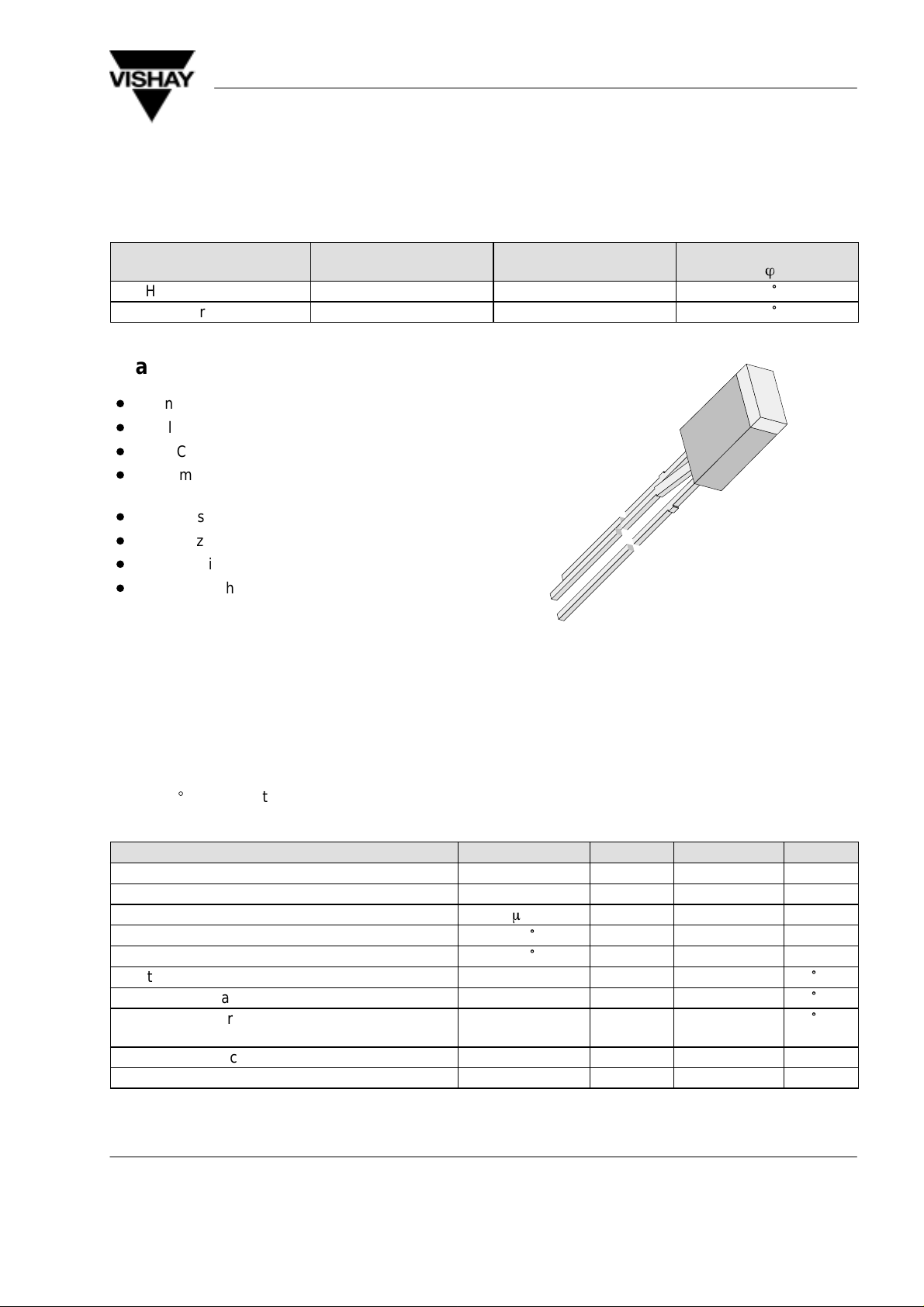
Bicolor Symbol LED
in 2.5 x 5 mm Untinted Top-Diffused Package
Color Type Technology Angle of Half Intensity
High efficiency red TLSV5100 GaAsP on GaP 50
Green TLSV5100G GaP on GaP 50
Features
D
Even luminance of the emitting surface
D
Ideal as flush mounted panel indicators
D
For DC and pulse operation
D
Color mixing possible due to separate
anode terminals
D
Luminous intensity selected into groups
D
Categorized for green color
D
Wide viewing angle
D
Common cathode
TLSV5100
±
ö
°
°
96 11496
Applications
Indicating and illumination purposes
Absolute Maximum Ratings
T
= 25_C, unless otherwise specified
amb
TLSV5100 ,TLSV5100G ,
Parameter Test Conditions Symbol Value Unit
Reverse voltage per diode V
DC forward current per diode I
Surge forward current per diode tp ≤ 10 ms I
Power dissipation per diode T
Total power dissipation T
Junction temperature T
Storage temperature range T
Soldering temperature t ≤ 5 s,
Thermal resistance junction/ambient per diode R
Thermal resistance junction/ambient total R
≤ 55°C P
amb
≤ 55°C P
amb
2 mm from body
R
F
FSM
V
tot
stg
T
sd
thJA
thJA
6 V
30 mA
1 A
100 mW
150 mW
j
100
–55 to +100
260
450 K/W
300 K/W
°
C
°
C
°
C
Document Number 83052
Rev. A1, 04-Feb-99
www.vishay .de • FaxBack +1-408-970-5600
1 (6)
TLSV5100
Vishay Telefunken
Optical and Electrical Characteristics
T
= 25_C, unless otherwise specified
amb
High efficiency red (TLSV5100 )
Parameter Test Conditions Type Symbol Min Typ Max Unit
Per diode
Luminous intensity IF = 10 mA, I
Vmin/IVmax
Dominant wavelength IF = 10 mA
Peak wavelength IF = 10 mA
Angle of half intensity IF = 10 mA ϕ ±50 deg
Forward voltage IF = 20 mA V
Reverse voltage IR = 10 mA V
Junction capacitance VR = 0, f = 1 MHz C
Green (TLSV5100G )
Parameter Test Conditions Type Symbol Min Typ Max Unit
Per diode
Luminous intensity IF = 10 mA, I
Vmin/IVmax
Dominant wavelength IF = 10 mA
Peak wavelength IF = 10 mA
Angle of half intensity IF = 10 mA ϕ ±50 deg
Forward voltage IF = 20 mA V
Reverse voltage IR = 10 mA V
Junction capacitance VR = 0, f = 1 MHz C
≥ 0.5 I
≥ 0.5 I
0.63 1 mcd
V
l
l
V
l
l
612 625 nm
d
p
F
R
j
635 nm
2 3 V
6 15 V
50 pF
0.63 1 mcd
562 575 nm
d
p
F
R
j
565 nm
2.4 3 V
6 15 V
50 pF
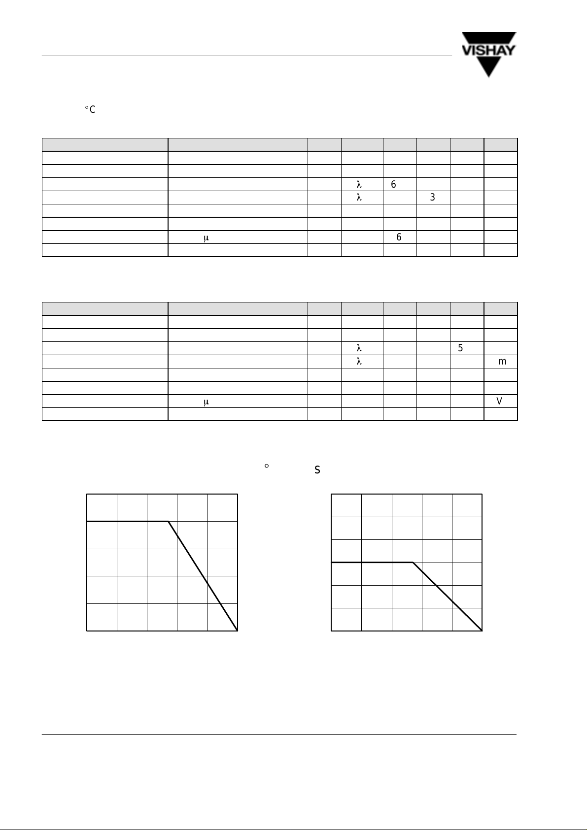
Typical Characteristics (T
125
100
75
50
V
25
P – Power Dissipation ( mW )
0
020406080
T
95 9983
Figure 1 Power Dissipation vs. Ambient Temperature
www.vishay .de • FaxBack +1-408-970-5600 Document Number 83052
2 (6)
– Ambient Temperature ( °C )
amb
= 25_C, unless otherwise specified)
amb
60
50
40
30
20
F
I – Forward Current ( mA )
10
100
0
020406080
T
95 9984
Figure 2 Forward Current vs. Ambient Temperature
– Ambient Temperature ( °C )
amb
100
Rev. A1, 04-Feb-99
 Loading...