Telefunken TCED4100G, TCED4100, TCED2100G, TCED2100, TCED1100G Datasheet
...
TCED1100(G) up to TCED4100
Vishay Telefunken
Rev. A3, 1 1–Jan–99234
Optocoupler with Photodarlington Output
Description
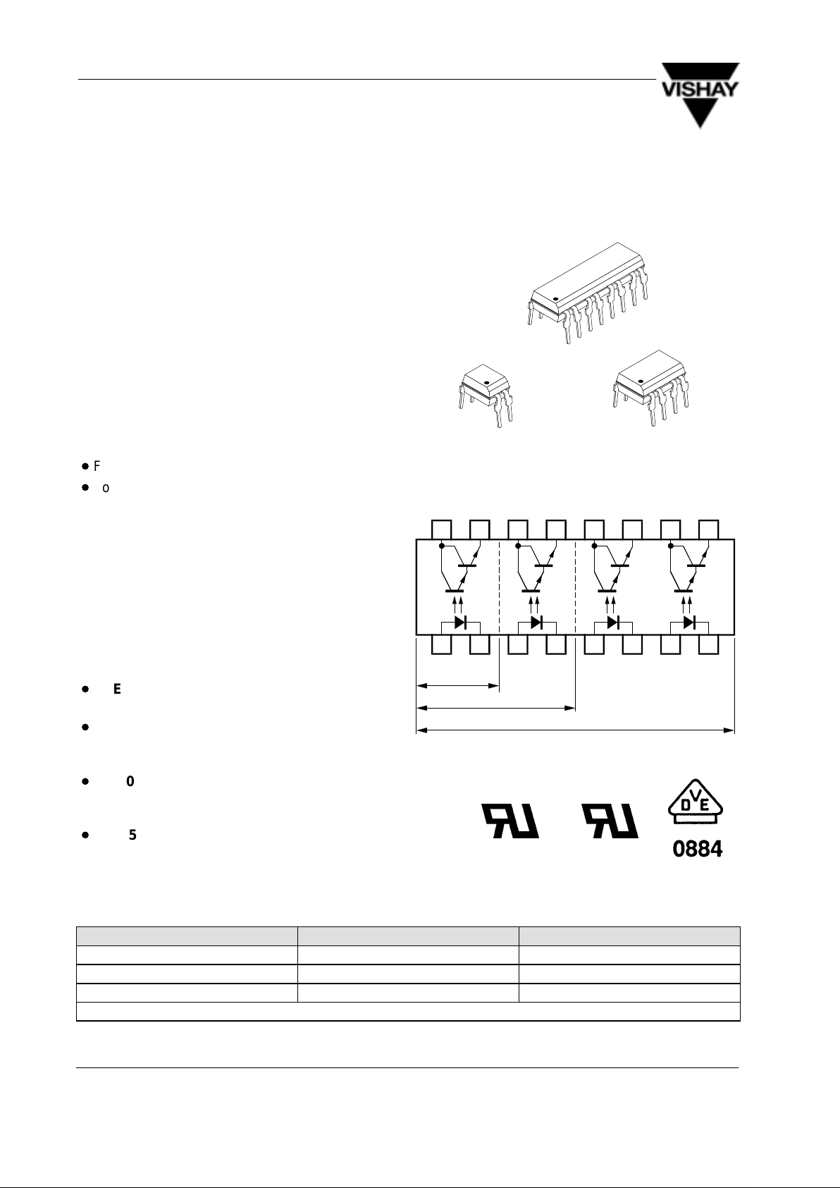
The TCED1 100/ TCED2100/ TCED4100 consists of
a phototransistor optically coupled to a gallium arsenide infrared-emitting diode in a 4-lead up to 16-lead
plastic dual inline package.
The elements are mounted on one leadframe using
a coplanar technique, providing a fixed distance
between input and output for highest safety
requirements.
Applications
Circuits for safe protective separation against
electrical shock according to safety class II
(reinforced isolation):
D
For appl. class I – IV at mains voltage ≤ 300 V
D
For appl. class I – III at mains voltage ≤ 600 V
according to VDE 0884, table 2, suitable for:
Switch-mode power supplies, line receiver,
computer peripheral interface, microprocessor
system interface.
VDE Standards
These couplers perform safety functions according
to the following equipment standards:
D
VDE 0884
Optocoupler for electrical safety requirements
D
IEC 950/EN 60950
Office machines (applied for reinforced
isolation for mains voltage ≤ 400 V
RMS
)
D
VDE 0804
Telecommunication apparatus and data
processing
D
IEC 65
Safety for mains-operated electronic and
related household apparatus
14925
Coll. Emitter
Anode Cath.
4 PIN
8 PIN
16 PIN
14580
C
Order Instruction
Ordering Code CTR Ranking Remarks
TCED1100/ TCED1 100G
1)
600% 4 Pin = Single channel
TCED2100 600% 8 Pin = Dual channel
TCED4100 600% 16 Pin = Quad channel
1)
G = Leadform 10.16 mm; G is not market on the body

TCED1100(G) up to TCED4100
Vishay Telefunken
Rev. A3, 1 1–Jan–99 235
Features
Approvals:
D
BSI: BS EN 41003, BS EN 60095 (BS 415),
BS EN 60950 (BS 7002),
Certificate number 7081 and 7402
D
FIMKO (SETI): EN 60950,
Certificate number 11992
D
Underwriters Laboratory (UL) 1577 recognized,
file number E-76222 – Double Protection
D
CSA (C–UL) 1577 recognized,
file number E-76222 – Double Protection
D
VDE 0884, Certificate number 115667
VDE 0884 related features:
D
Rated impulse voltage (transient overvoltage)
V
IOTM
= 8 kV peak
D
Isolation test voltage
(partial discharge test voltage) V
pd
= 1.6 kV
D
Rated isolation voltage (RMS includes DC)
V
IOWM
= 600 V
RMS
(848 V peak)
D
Rated recurring peak voltage (repetitive)
V
IORM
= 600 V
RMS
D
Creepage current resistance according to
VDE 0303/IEC 1 12
Comparative Tracking Index: CTI ≥ 175
D
Thickness through insulation ≥ 0.75 mm
D
Internal creepage distance > 4 mm
General features:
D
Isolation materials according to UL94-VO
D
Pollution degree 2 (DIN/VDE 01 10 / resp. IEC 664)
D
Climatic classification 55/100/21 (IEC 68 part 1)
D
Special construction:
Therefore, extra low coupling capacity of
typical 0.2 pF, high Common Mode Rejection
D
Low temperature coefficient of CTR
D
G = Leadform 10.16 mm;
provides creepage distance > 8 mm,
for TCED2100/ TCED4100 optional;
suffix letter ‘G’ is not marked on the optocoupler
D
Coupling System U
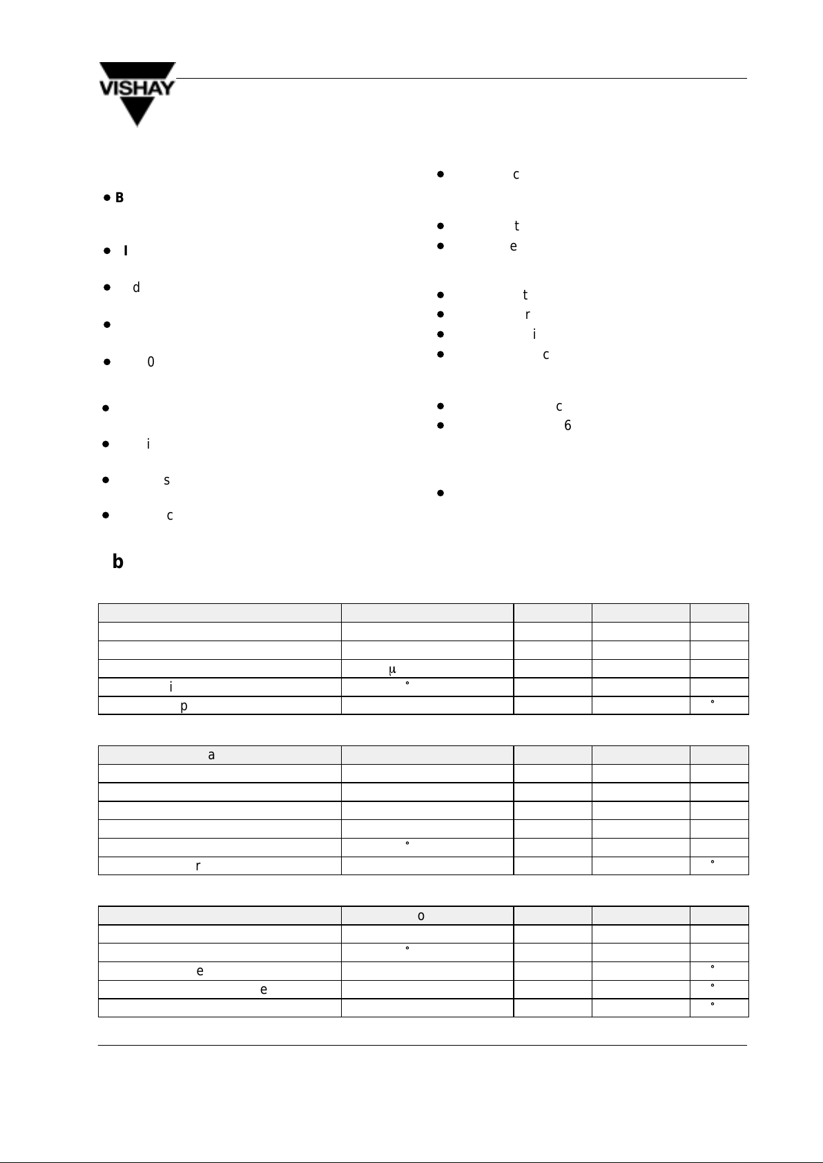
Absolute Maximum Ratings
Input (Emitter)
Parameter Test Conditions Symbol Value Unit
Reverse voltage V
R
6 V
Forward current I
F
60 mA
Forward surge current tp ≤ 10 ms I
FSM
1.5 A
Power dissipation T
amb
≤ 25°C P
V
100 mW
Junction temperature T
j
125
°
C
Output (Detector)
Parameter Test Conditions Symbol Value Unit
Collector emitter voltage V
CEO
35 V
Emitter collector voltage V
ECO
7 V
Collector current I
C
80 mA
Collector peak current tp/T = 0.5, tp ≤ 10 ms I
CM
100 mA
Power dissipation T
amb
≤ 25°C P
V
150 mW
Junction temperature T
j
125
°
C
Coupler
Parameter Test Conditions Symbol V alue Unit
AC isolation test voltage (RMS) t = 1 min V
IO
5 kV
Total power dissipation T
amb
≤ 25°C P
tot
250 mW
Operating ambient temperature range T
amb
–40 to +100
°
C
Storage temperature range T
stg
–55 to +125
°
C
Soldering temperature 2 mm from case t ≤ 10 s T
sd
260
°
C

TCED1100(G) up to TCED4100
Vishay Telefunken
Rev. A3, 1 1–Jan–99236
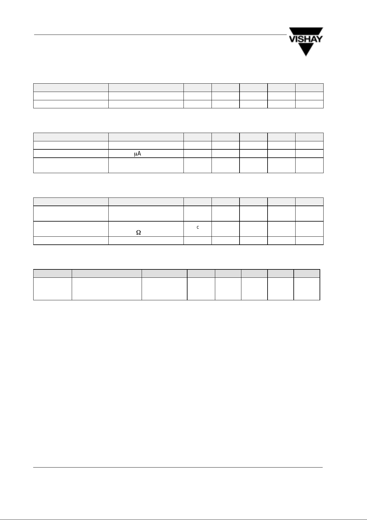
Electrical Characteristics (T
amb
= 25°C)
Input (Emitter)
Parameter Test Conditions Symbol Min. Typ. Max. Unit
Forward voltage IF = 20 mA V
F
1.15 1.4 V
Junction capacitance VR = 0 V, f = 1 MHz C
j
50 pF
Output (Detector)
Parameter Test Conditions Symbol Min. Typ. Max. Unit
Collector emitter voltage IC = 1 mA V
CEO
32 V
Emitter collector voltage IE = 100 mA V
ECO
7 V
Collector emitter cut-off
current
VCE = 10 V, If = 0, E = 0 I
CEO
15 100 nA
Coupler
Parameter Test Conditions Symbol Min. Typ. Max. Unit
Collector emitter
saturation voltage
IF = 20 mA, IC = 5 mA V
CEsat
1 V
Cut-off frequency VCE = 5 V, IF = 10 mA,
R
L
= 100
W
f
c
10 kHz
Coupling capacitance f = 1 MHz C
k
0.3 pF
Current Transfer Ratio (CTR)
Parameter Test Conditions Type Symbol Min. Typ. Max. Unit
IC/I
F
VCE = 2 V, IF = 1 mA TCED1100(G)/
TCED2100/
TCED4100
CTR 6.0 8.0
 Loading...