

Datasheet TC500COE, TC500ACPE, TC500ACOE, TC510CPF, TC510COG Datasheet (TelCom Semiconductor)
...
PRECISION ANALOG FRONT ENDS
EVALUATION
KIT
AVAILABLE
TC500
TC500A
TC510
TC514
1
FEATURES
■ Precision (up to 17 Bits) A/D Converter "Front End"
■ 3-Pin Control Interface to Microprocessor
■ Flexible: User Can Trade-Off Conversion Speed
for Resolution
■ Single Supply Operation (TC510/514)
■ 4 Input, Differential Analog MUX (TC514)
■ Automatic Input Voltage Polarity Detection
■ Low Power Dissipation ...........TC500/500A: 10mW
TC510/514: 18mW
■ Wide Analog Input Range .......±4.2V (TC500A/510)
■ Directly Accepts Bipolar and Differential Input
Signals
ORDERING INFORMATION
Part No. Package Temp. Range
TC500ACOE 16-Pin SOIC 0°C to +70°C
T
C500ACPE 16-Pin Plastic DIP (Narrow) 0°C to +70°C
TC500COE 16-Pin SOIC 0°C to +70°C
TC500CPE 16-Pin Plastic DIP (Narrow) 0°C to +70°C
TC510COG 24-Pin SOIC 0°C to +70°C
TC510CPF 24-Pin Plastic DIP (300 Mil.) 0°C to +70°C
TC514COI 28-Pin SOIC 0°C to +70°C
TC514CPJ 28-Pin Plastic DIP (300 Mil.) 0°C to +70°C
TC500EV Evaluation Kit for TC500/500A/510/514
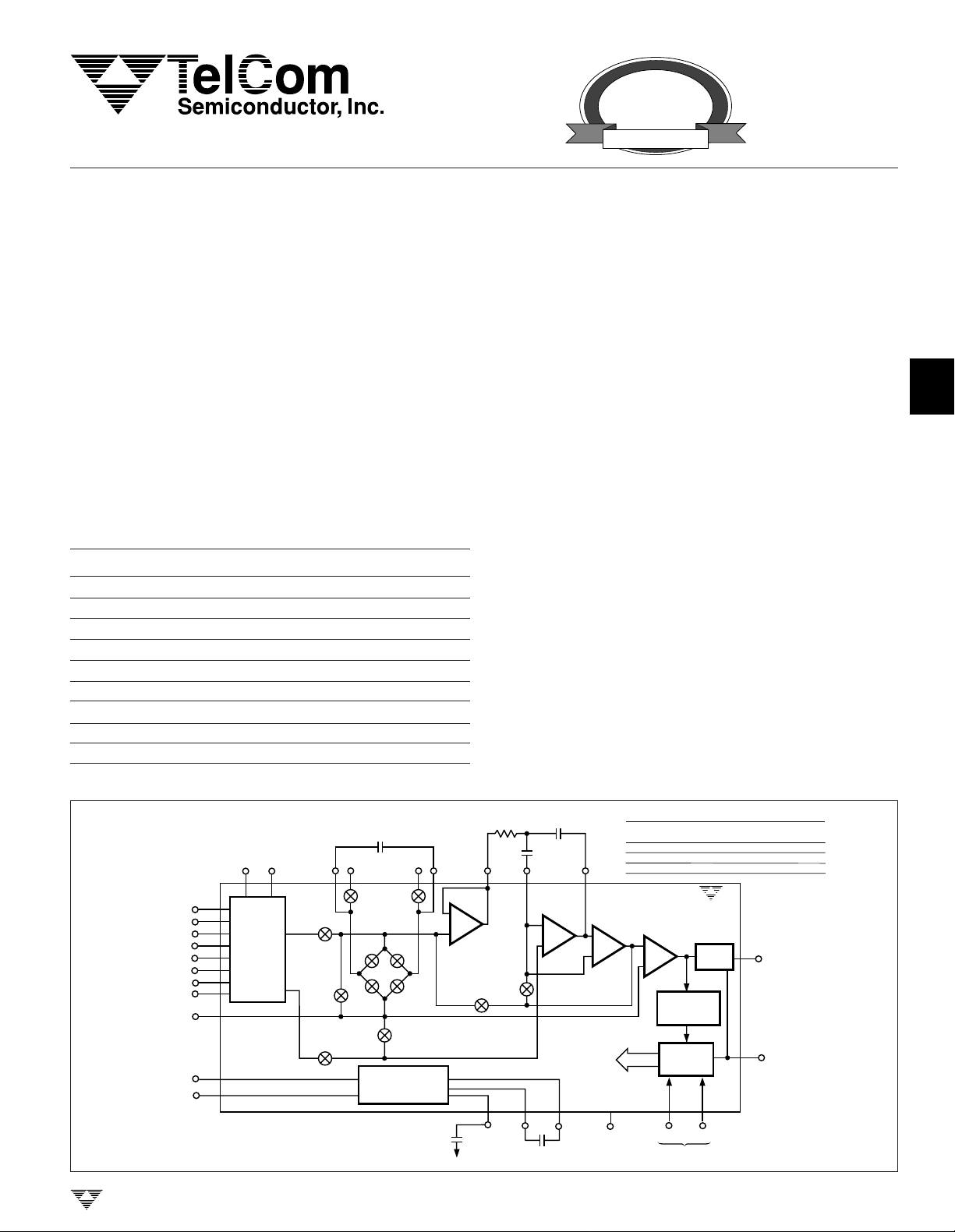
FUNCTIONAL BLOCK DIAGRAM
C
REF
CH1
CH2
CH3
CH4
CH1
CH2
CH3
CH4
ACOM
OSC
+
C
+
REF
SW
SW
SW
V
REF
SW
I
SW
Z
SW
I
A1
A0
+
+
+
+
–
–
–
–
V
S
DIF.
MUX
(TC514)
–
V
REF
SW
R
R
–
+
SW
RI
RI
–
+
SW
RI
RI
SW
1
DC-TO-DC
CONVERTER
(TC510 & TC514)
–
C
REF
BUFFER
–
+
GENERAL DESCRIPTION
The TC500/500A/510/514 family are precision analog
front ends that implement dual slope A/D converters having
a maximum resolution of 17 bits plus sign. As a minimum,
each device contains the integrator, zero crossing comparator and processor interface logic. The TC500 is the base
(16 bit max) device and requires both positive and negative
power supplies. The TC500A is identical to the TC500,
except it has improved linearity allowing it to operate to a
maximum resolution of 17 bits. The TC510 adds an onboard negative power supply converter for single supply
operation. The TC514 adds both a negative power supply
converter and a 4 input differential analog multiplexer.
Each device has the same processor control interface
consisting of 3 wires: control inputs A and B and zerocrossing comparator output (CMPTR). The processor manipulates A, B to sequence the TC5xx through four phases
of conversion: Auto Zero, Integrate, Deintegrate and Integrator Zero. During the Auto Zero phase, offset voltages in
the TC5xx are corrected by a closed-loop feedback mechanism. The input voltage is applied to the integrator during the
Integrate phase. This causes an integrator output dv/dt
directly proportional to the magnitude of the input voltage.
The higher the input voltage, the greater the magnitude of
the voltage stored on the integrator during this phase. At the
start of the Deintegrate phase, an external voltage reference
is applied to the integrator, and at the same time, the external
host processor starts its on-board timer.
CONTROL LOGIC
A B
0 0 ZERO INTEGRATOR OUTPUT
0 1 AUTO-ZERO
1 0 SIGNAL INTEGRATE
1 1 DEINTEGRATE
CMPTR 2
–
+
POLARITY
DETECTION
PHASE
DECODING
LOGIC
SW
INT
AZ
Z
–
C
INT
C
AZ
INTEGRATOR
–
+
CONTROL
–
CAP
CAP
C
INT
CMPTR 1
+
–
ANALOG
SWITCH
SIGNALS
+
R
C
BUF
SW
IZ
V
OUT
CONVERTER STATE
TC500
TC500A
TC510
TC514
LEVEL
SHIFT
The processor main-
CMPTR
OUTPUT
DGND
2
3
4
5
6
7
TELCOM SEMICONDUCTOR, INC.
1.0µF
C
–
OUT
1.0µF
V
SS
(TC500
TC500A)
CONTROL LOGIC
BA
8
TC500/A/510/514-3 10/3/96
3-19
TC500
TC500A
TC510
TC514
PRECISION ANALOG FRONT ENDS
GENERAL DESCRIPTION (Cont.)
tains this state until a transition occurs on the CMPTR output,
at which time the processor halts its timer. The resulting
timer count is the converted analog data. Integrator Zero
(the final phase of conversion) removes any residue remaining in the integrator in preparation for the next
conversion.
The TC500/500A/510/514 offer high resolution (up to 17
bits) superior 50Hz/60Hz noise rejection, low power operation, minimum I/O connections, low input bias currents and
lower cost compared to other converter technologies having
similar conversion speeds.
ABSOLUTE MAXIMUM RATINGS
*
TC510/514 Positive Supply Voltage
(VDD to GND) .................................................. +10.5V
TC500/500A Supply Voltage
(V
to VSS) ....................................................... +18V
DD
TC500/500A Positive Supply Voltage
(VDD to GND) ..................................................... +12V
ELECTRICAL CHARACTERISTICS: TC510/514: V
specified. CAZ = C
TC500/500A Negative Supply Voltage
(VSS to GND) ...................................................... – 8V
Analog Input Voltage (V
+
IN
_
or V
) ....................VDD to V
IN
Logic Input Voltage .................. VDD +0.3V to GND – 0.3V
Voltage on OSC ..... – 0.3V to (VDD +0.3V) for VDD < 5.5V
Ambient Operating Temperature Range ...... 0°C to +70°C
Storage Temperature Range ................ – 65°C to +150°C
Lead Temperature (Soldering, 10 sec) ................. +300°C
* Static-sensitive device. Unused devices must be stored in conductive
material. Protect devices from static discharge and static fields. Stresses
above those listed under "Absolute Maximum Ratings" may cause permanent damage to the device. These are stress ratings only and functional
operation of the device at these or any other conditions above those
indicated in the operation sections of the specifications is not implied.
Exposure to absolute maximum rating conditions for extended periods may
affect device reliability.
= +5V, TC500/500A: V
DD
= 0.47 µF
REF
= ±5V unless otherwise
S
SS
TA = +25°C TA = 0°C to +70°C
Symbol Parameter Test Conditions Min Typ Max Min Typ Max Unit
Analog
Resolution Note 1 60 — — — — — µV
ZSE Zero-Scale Error TC500/510/514 — — 0.005 — 0.005 0.012 % F.S.
with Auto Zero Phase TC500A — — 0.003 — 0.003 0.009
ENL End Point Linearity
NL Best Case Straight
Line Linearity
ZS
TC
SYE Full-Scale Symmetry Note 3 — 0.01 — — 0.03 — % F.S.
FS
TC
I
IN
V
CMR
V
REF
Zero-Scale Over Operating — — — 1 2 µV/°C
Temperature Temperature Range
Coefficient
Error (Roll-Over Error)
Full-Scale Temperature Over Operating — — — — 10 —
Coefficient Temperature Range
Input Current VIN = 0V — 6 — — — — pA
Common-Mode VSS +1.5 — VDD – 1.5 V
Voltage Range
Integrator Output Swing VSS +0.9 — VDD – 0.9 VSS +0.9 — VSS +0.9 V
Analog Input Signal RangeACOM = GND = 0V VSS +1.5 — VDD – 1.5 V
Voltage Reference Range V
TC500/510/514, Notes 1, 2,
TC500A
TC500/510/514, Notes 1, 2,
TC500A
External Reference
TC = 0ppm/°C
_
+
V
REF
REF
— 0.005 0.015 — 0.015 0.060
— — 0.010 — 0.010 0.045
— 0.003 0.008 — — —
— — 0.005 — — —
+1.5 — VDD – 1.5 V
SS
+1.5 — V
SS
V
+1 — VDD – 1 V
SS
+1 — VDD – 1 V
SS
+1.5 V
SS
% F.S.
% F.S.
% F.S.
% F.S.
ppm/°C
3-20
TELCOM SEMICONDUCTOR, INC.

PRECISION ANALOG FRONT ENDS
ELECTRICAL CHARACTERISTICS: (Cont.)
TC500
TC500A
TC510
TC514
1
T
Symbol Parameter Test Conditions Min Typ Max Min Typ Max Unit
Digital
V
OH
V
OL
V
IH
V
IL
I
L
t
D
Multiplexer (TC514 Only)
R
DS
ON
Power (TC510/514 Only)
I
S
P
D
V
DD
R
OUT
I
OUT
Power (TC500/500A Only)
I
S
P
D
V
DD
V
SS
NOTES: 1. Integrate time ≥ 66msec, auto-zero time ≥ 66msec, V
Comparator Logic 1, I
Output High
Comparator Logic 0, I
Output Low
Logic 1, Input High Voltage 3.5 — — 3.5 — — V
Logic 0, Input Low Voltage — — 1 — — 1 V
Logic Input Current Logic 1 or 0 — — — — 0.3 — µA
Comparator Delay — 2 — — 3 — µsec
Maximum Input Voltage VDD = 5V – 2.5 — 2.5 – 2.5 — 2.5 V
Drain/Source ON Resistance VDD = 5V — 6 10 — — — kΩ
Supply Current VDD = 5V, A = 1, B = 1 — 1.8 2.4 — — 3.5 mA
Power Dissipation VDD = 5V — 18 — — — — mW
Positive Supply 4.5 — 5.5 4.5 — 5.5 V
Operating Voltage Range
Operating Source Resistance I
Oscillator Frequency (Note 3) — 100 — — — — kHz
Maximum Current Out VDD = 5V — — – 10 — — – 10 mA
Supply Current VS = ±5V, A = B = 1 — 1 1.5 — — 2.5 mA
Power Dissipation V
Positive Supply 4.5 — 7.5 4.5 — 7.5 V
Operating Voltage Range
Negative Supply – 4.5 — – 7.5 – 4.5 — – 7.5 V
Operating Voltage Range
2. End point linearity at ±1/4, ±1 /2, ±3/4 F.S. after full-scale adjustment.
3. Roll-over error is related to C
INT
, C
REF
= 400µA4——4——V
SOURCE
= 2.1mA — — 0.4 — — 0.4 V
SINK
= 10mA — 60 85 — — 100 Ω
OUT
= 5V, VSS = – 5V — 10 — — — — mW
DD
(peak) ≈ 4V.
INT
, CAZ characteristics.
= +25°C TA = 0°C to +70°C
A
2
3
4
5
6
TELCOM SEMICONDUCTOR, INC.
7
8
3-21

TC500
TC500A
TC510
TC514
PIN CONFIGURATIONS
PRECISION ANALOG FRONT ENDS
C
V
C
ACOM
C
REF
C
REF
V
REF
–
V
OUT
C
INT
C
AZ
BUF
ACOM
–
C
REF
+
C
REF
–
V
REF
+
V
REF
N/C
N/C
N/C
INT
–
+
–
SS
AZ
1
2
3
4
5
6
7
8
1
2
3
4
5
6
TC510CPF
7
8
9
10
11
12
TC500/
TC500A
CPE
V
16
DD
15
DIGITAL GND
14
CMPTR OUT
B
13BUF
12
A
+
V
11
IN
–
V
10
IN
+
V
9
REF
24
CAP
23
DGND
22
CAP
V
21
DD
20
OSC
CMPTR OUT
19
A
18
17
B
+
V
16
IN
15
V
IN
14
N/C
13
N/C
C
INT
V
SS
C
AZ
BUF
ACOM
–
C
REF
+
C
REF
–
V
REF
–
–
+
V
C
OUT
INT
C
AZ
BUF
ACOM
–
C
REF
+
C
REF
–
V
REF
+
V
REF
–
N/C
N/C
N/C
1
2
3
4
5
6
7
8
9
10
11
12
1
2
3
4
TC500/
5
TC500A
COE
6
7
8
TC510COG
16
15
14
13
12
11
10
9
24
23
22
21
20
19
18
17
16
15
14
13
V
DD
DIGITAL GND
CMPTR OUT
B
A
+
V
IN
–
V
IN
+
V
REF
–
CAP
DGND
+
CAP
V
DD
OSC
CMPTR OUT
A
B
+
V
IN
–
V
IN
N/C
N/C
3-22
–
V
OUT
C
INT
C
AZ
BUF
ACOM
–
C
REF
+
C
REF
–
V
REF
+
V
REF
CH4
CH3
CH2
CH1
N/C
–
–
–
–
1
2
3
4
5
6
7
8
9
10
11
12
13
14
TC514CPJ
28
CAP
27
DGND
26
CAP
V
25
DD
24
OSC
CMPTR OUT
23
A
22
B
21
A0
20
A1
19
18
CH1
17
CH2
16
CH3
CH4
15
–
–
+
+
+
+
+
V
OUT
C
INT
C
AZ
BUF
ACOM
–
C
REF
+
C
REF
–
V
REF
+
V
REF
CH4
CH3
CH2
CH1
N/C
1
2
3
4
5
6
TC514COI
7
8
9
–
10
–
11
–
12
–
13
14
28
27
26
25
24
23
22
21
20
19
18
17
16
15
–
CAP
DGND
+
CAP
V
DD
OSC
CMPTR OUT
A
B
A0
A1
+
CH1
+
CH2
+
CH3
+
CH4
TELCOM SEMICONDUCTOR, INC.

PRECISION ANALOG FRONT ENDS
PIN DESCRIPTION
TC500
TC500A
TC510
TC514
1
Pin No Pin No Pin No
(TC500, 500A) (TC510) (TC514) Symbol Description
122C
2 Not Used Not Used V
333CAZAuto-zero input. The Auto-zero capacitor connection.
4 4 4 BUF Buffer output. The Integrator capacitor connection.
5 5 5 ACOM This pin is grounded in most applications. It is recommended that
666C
777C
888V
999V
10 15 Not Used V
11 16 Not Used V
12 18 22 A Input. Converter phase control MSB. (See input B.)
13 17 21 B Input. Converter phase control LSB. The states of A, B place the
14 19 23 CMPTR OUT Zero crossing comparator output. CMPTR is HIGH during the
15 23 27 DGND Input. Digital ground.
16 21 25 V
22 26 CAP
24 28 CAP
11V
20 24 OSC Oscillator control input. The negative power supply converter normally
18 CH1
13 CH1
17 CH2
12 CH2
16 CH3
11 CH3
15 CH4
INT
SS
–
REF
+
REF
–
REF
+
REF
–
IN
+
IN
DD
–
OUT
Integrator output. Integrator capacitor connection.
Negative power supply input (TC500/500A only).
–
–
or C
ACOM and the input common pin (V
analog common mode range (CMR).
Input. Negative reference capacitor connection.
Input. Positive reference capacitor connection.
Input. External voltage reference (–) connection.
Input. External voltage reference (+) connection.
Negative analog input.
Positive analog input.
TC5xx in one of four required phases. A conversion is complete
when all four phases have been executed:
Phase control input pins: AB =
Integration phase when a
and is LOW when a negative input voltage is being integrated. A
HIGH-to-LOW transition on CMPTR signals the processor that the
Deintegrate phase is completed. CMPTR is undefined during the
Auto-Zero phase. It should be monitored to time the Integrator Zero
phase (see text).
Input. Power supply positive connection.
+
Input. Negative power supply converter capacitor (+) connection.
–
Input. Negative power supply converter capacitor (–) connection.
Output. Negative power supply converter output and reservoir
capacitor connection. This output can be used to power other
devices in the circuit requiring a negative bias voltage.
runs at a frequency of 100kHz. The converter oscillator frequency can
be slowed down (to reduce quiescent current) by connecting an
external capacitor between this pin and VDD. (See Typical Characteristics Curves).
+
Positive analog input pin. MUX channel 1.
–
Negative analog input pin. MUX channel 1.
+
Positive analog input pin. MUX channel 2.
–
Negative analog input pin. MUX channel 2.
+
Positive analog input pin. MUX channel 3.
–
Negative analog input pin. MUX channel 3.
+
Positive analog input pin. MUX channel 4.
positive input voltage is being integrated
IN
00: Integrator Zero
01: Auto Zero
10: Integrate
11: Deintegrate
) be within the
HN
2
3
4
5
6
7
8
TELCOM SEMICONDUCTOR, INC.
3-23
TC500
TC500A
TC510
TC514
PIN DESCRIPTION (Cont.)
Pin No Pin No Pin No
(TC500/A) (TC510) (TC514) Symbol Description
10 CH4
20 A0 Multiplexer input channel select input LSB. (See A1).
19 A1 Multiplexer input channel select input MSB.
GENERAL THEORY OF OPERATION
Dual-Slope Conversion Principles (Figure 2)
Actual data conversion is accomplished in two phases:
input signal Integration and reference voltage Deintegration.
The integrator output is initialized to 0V prior to the start
of Integration. During Integration, analog switch S1 connects VIN to the integrator input where it is maintained for a
fixed time period (t
integrator output to depart 0V at a rate determined by the
magnitude of
VIN, and a direction determined by the
of VIN. The Deintegration phase is initiated immediately at
the expiration of t
). The application of VIN causes the
INT
.
INT
–
Negative analog input pin. MUX channel 4
Phase control input pins: A1, A0 =
polarity
PRECISION ANALOG FRONT ENDS
00 = Channel 1
01 = Channel 2
10 = Channel 3
11 = Channel 4
During Deintegration, S1 connects a reference voltage
(having a polarity opposite that of VIN) to the integrator input.
At the same time, an external precision timer is started. The
Deintegration phase is maintained until the comparator
output changes state, indicating the integrator has returned
to its starting point of 0V. When this occurs, the precision
timer is stopped. The Deintegration time period (t
measured by the precision timer, is directly proportional to
the magnitude of the applied input voltage.
A simple mathematical equation relates the Input
Signal, Reference Voltage and Integration time:
DEINT
), as
ANALOG
INPUT
(VIN)
OUTPUT
INTEGRATOR
T
INT
VOLTAGE
T
DEINT
REF
±
V
V
IN
IN
S1
' V
' 1/2 V
C
INT
R
INT
FULL SCALE
FULL SCALE
Figure 2. Basic Dual-Slope Converter
INTEGRATOR
–
+
SWITCH DRIVER
POLARITY
CONTROL
V
SUPPLY
V
INT
V
INT
–
+
PHASE
CONTROL
TC510
COMPARATOR
CONTROL
LOGIC
AB
I/O
MICROCOMPUTER
ROM
RAM
TIMER
COUNTER
CMPTR OUT
3-24
TELCOM SEMICONDUCTOR, INC.

PRECISION ANALOG FRONT ENDS
TC500
TC500A
TC510
TC514
1
1 t
R
INT CINT
where:
V
t
t
For a constant VIN:
The dual-slope converter accuracy is unrelated to the
integrating resistor and capacitor values as long as they are
stable during a measurement cycle.
An inherent benefit is noise immunity. Input noise spikes
are integrated (averaged to zero) during the integration
periods. Integrating ADCs are immune to the large conversion errors that plague successive approximation converters in high-noise environments.
Integrating converters provide inherent noise rejection
with at least a 20dB/decade attenuation rate. Interference
signals with frequencies at integral multiples of the integration period are, theoretically, completely removed since the
average value of a sine wave of frequency (1/t) averaged
over a period (t) is zero.
Integrating converters often establish the integration
period to reject 50/60Hz line frequency interference signals.
The ability to reject such signals is shown by a normal mode
rejection plot (Figure 4). Normal mode rejection is limited in
practice to 50 to 65dB, since the line frequency can deviate
by a few tenths of a percent (Figure 3).
= Reference Voltage
REF
= Signal Integration time (fixed)
INT
= Reference Voltage Integration time (variable)
DEINT
VIN = V
REF
80
∫
INT
0
t
DEINT
t
VIN (t) dt =
INT
V
R
REF tDEINT
INT CINT
30
T = MEASUREMENT
PERIOD
20
10
NORMAL MODE REJECTION (dB)
0
0.1/T 1/T 10/T
INPUT FREQUENCY
Figure 4.. Integrating Converter Normal Mode Rejection
TC500/500A/510/514 CONVERTER OPERATION
The TC500/500A/510/514 incorporates an Auto zero
and Integrator phase in addition to the input signal Integrate
and reference Deintegrate phases. The addition of these
phases reduce system errors and calibration steps, and
shorten overrange recovery time. A typical measurement
cycle uses all four phases in the following order:
(1) Auto zero
(2) Input signal integration
(3) Reference deintegration
(4) Integrator output zero
The internal analog switch status for each of these
phases is summarized in Table 1. This table is referenced
to the
Functional Block Diagram
sheet.
on the first page of this data
2
3
4
5
6
70
t = 0.1 sec
60
50
40
NORMAL
MODE
REJECTION
30
DEV = DEVIATION FROM 60 Hz
NORMAL MODE REJECTION (dB)
t = INTEGRATION PERIOD
20
0.01 0.1
LINE FREQUENCY DEVIATION FROM 60 Hz (%)
Figure 3. Line Frequency Deviation
TELCOM SEMICONDUCTOR, INC.
= 20 LOG
π
SIN 60 t (1 ± )
p
60 t (1 ± )
DEV
100
DEV
100
1.0
Auto-Zero Phase (AZ)
During this phase, errors due to buffer, integrator and
comparator offset voltages are nulled out by charging C
(auto-zero capacitor) with a compensating error voltage.
The external input signal is disconnected from the
internal circuitry by opening the two SWI switches. The
internal input points connect to analog common. The reference capacitor is charged to the reference voltage potential
through SWR. A feedback loop, closed around the integrator
and comparator, charges the CAZ capacitor with a voltage to
compensate for buffer amplifier, integrator and comparator
offset voltages.
AZ
3-25
7
8

PRECISION ANALOG FRONT ENDS
TC500
TC500A
TC510
TC514
Table 1. Internal Analog Gate Status
Internal Analog Gate Status
Conversion Phase SW
Auto-Zero (A = 0, B = 1) Closed Closed Closed
Input Signal Integration Closed
(A = 1, B = 0)
Reference Voltage Closed* Closed
Deintegration (A =1, B= 1)
Integrator Output Zero Closed Closed Closed
(A = 0, B = 0)
*Assumes a positive polarity input signal. SW
I
–
would be closed for a negative input signal.
RI
SW
+
RI
Analog Input Signal Integration Phase (INT)
The TC5xx integrates the differential voltage between
+
the (V
) and (V
IN
within the device's common-mode range V
–
) inputs. The differential voltage must be
IN
.
CMR
The input signal polarity is normally checked via software at the end of this phase: CMPTR = 1 for positive
polarity; CMPTR = 0 for negative polarity.
Reference Voltage Deintegration Phase (DINT)
The previously charged reference capacitor is connected with the proper polarity to ramp the integrator output
back to zero. An externally-provided, precision timer is used
to measure the duration of this phase. The resulting time
measurement is proportional to the magnitude of the applied
input voltage.
–
SW
RI
SW
Z
SW
R
SW
1
SW
IZ
voltage range, common-mode rejection is typically 80dB.
Full accuracy is maintained, however, when the inputs are
no less than 1.5V from either supply.
The integrator output also follows the common-mode
voltage. The integrator output must not be allowed to saturate. A worst-case condition exists, for example, when a
large, positive common-mode voltage with a near full-scale
negative differential input voltage is applied. The negative
input signal drives the integrator positive when most of its
swing has been used up by the positive common-mode
voltage. For these critical applications, the integrator swing
can be reduced. The integrator output can swing within 0.9V
of either supply without loss of linearity.
Analog Common
Integrator Output Zero Phase (IZ)
This phase guarantees the integrator output is at 0V
when the Auto Zero phase is entered and that only system
offset voltages are compensated. This phase is used at the
end of the reference voltage deintegration phase and MUST
be used for ALL TC5xx applications having resolutions of 12
bits or more. If this phase is not used, the value of the AutoZero capacitor (CAZ) must be about 2 to 3 times the value of
the integration capacitor (C
) to reduce the effects of
INT
charge-sharing. The Integrator Output Zero phase should
be programmed to operate until the Output of the Comparator returns "HIGH". The overall Timing System is shown in
Figure 8.
ANALOG SECTION
+
Differential Inputs (V
The TC5xx operates with differential voltages within the
input amplifier common-mode range. The amplifier common-mode range extends from 1.5V below positive supply
to 1.5V above negative supply. Within this common-mode
3-26
IN
, V
–
IN
)
Analog common is used as V
zero and reference deintegrate. If V
return during system-
IN
–
is different from analog
IN
common, a common-mode voltage exists in the system.
This signal is rejected by the excellent CMR of the converter.
In most applications, V
(i.e., power supply common). A common-mode voltage will
exist when V
–
is not connected to analog common.
IN
Differential Reference
–
will be set at a fixed known voltage
IN
+
REF
, V
–
REF
)
(V
The reference voltage can be anywhere within 1V of the
power supply voltage of the converter. Roll-over error is
caused by the reference capacitor losing or gaining charge
due to stray capacitance on its nodes. The difference in
reference for (+) or (–) input voltages will cause a roll-over
error. This error can be minimized by using a large reference
capacitor in comparison to the stray capacitance.
Phase Control Inputs (A, B)
The A, B unlatched logic inputs select the TC5xx operating phase. The A, B inputs are normally driven by a
microprocessor I/O port or external logic.
TELCOM SEMICONDUCTOR, INC.

PRECISION ANALOG FRONT ENDS
TC500
TC500A
TC510
TC514
1
Comparator Output
By monitoring the comparator output during the fixed
signal integrate time, the input signal polarity can be determined by the microprocessor controlling the conversion.
The comparator output is HIGH for positive signals and LOW
for negative signals during the signal-integrate phase (see
timing diagram).
During the reference deintegrate phase, the comparator
output will make a HIGH-to-LOW transition as the integrator
output ramp crosses zero. The transition is used to signal the
processor that the conversion is complete.
REFERENCE
DEINTEGRATE
ZERO
CROSSING
INTEGRATOR
OUTPUT
COMPARATOR
OUTPUT
SIGNAL
INTEGRATE
The internal comparator delay is 2µsec, typically. Figure
5 shows the comparator output for large positive and negative signal inputs. For signal inputs at or near zero volts,
however, the integrator swing is very small. If commonmode noise is present, the comparator can switch several
times during the beginning of the signal-integrate period. To
ensure that the polarity reading is correct, the comparator
output should be read and stored at the end of the signal
integrate phase.
The comparator output is undefined during the AutoZero Phase and is used to time the Integrator Output Zero
phase. (See
section).
INTEGRATOR
COMPARATOR
Integrator Output Zero Phase of System Timing
SIGNAL
INTEGRATE
OUTPUT
OUTPUT
REFERENCE
DEINTEGRATE
ZERO
CROSSING
2
3
4
5
TELCOM SEMICONDUCTOR, INC.
B. Negative Input SignalA. Positive Input Signal
6
Figure 5. Comparator Output
7
8
3-27

TC500
TC500A
TC510
TC514
PRECISION ANALOG FRONT ENDS
APPLICATIONS
Component Value Selection
The procedure outlined below allows the user to arrive
at values for the following TC5xx design variables:
(1) Integration Phase Timing
(2) Integrator Timing Components (R
(3) Auto Zero and Reference Capacitors
(4) Voltage Reference
Select Integration Time
Integration time must be picked as a multiple of the
period of the line frequency. For example, t
33msec, 66msec and 132msec maximize 60Hz line rejection.
D
and IZ Phase Timing
INT
The duration of the DINT phase is a function of the
amount of voltage stored on the integrator during TINT, and
the value of V
. The DINT phase must be initiated imme-
REF
diately following INT and terminated when an integrator
output zero-crossing is detected. In general, the maximum
number of counts chosen for DINT is twice that of INT (with
V
chosen at V
REF
Calculate Integrating Resistor (R
(max)/2).
IN
INT
The desired full-scale input voltage and amplifier output
current capability determine the value of R
and integrator amplifiers each have a full-scale current of
20µA.
The value of R
follows:
R
(in MΩ) =
INT
where: V
R
IN MAX
=Integrating Resistor (in MΩ)
INT
For loop stability, R
Select Reference (C
C
and C
REF
AZ
is therefore directly calculated as
INT
V
IN MAX
20
= Maximum input voltage (full count voltage)
should be ≥ 50kΩ.
INT
) and Auto Zero (CAZ) Capacitors
REF
must be low leakage capacitors (such as
polypropylene). The slower the conversion rate, the larger
the value C
and C
AZ
C
may also be used to limit roll-over errors.
REF
must be. Recommended capacitors for C
REF
are shown in Table 1. Larger values for CAZ and
, C
INT
)
INT
times of
INT
)
. The buffer
INT
REF
Table 1. C
REF
and C
Selection
AZ
Conversions Typical Value of Suggested *
Per Second C
REF
, C
(µF) Part Number
AZ
>7 0.1 WIMA MK12 .1/63/20
2 to 7 0.22 WIMA MK12 .22/63/20
2 or less 0.47 WIMA MK12 .47/63/20
*WIMA Corp. listing on the last page of this data sheet.
Calculate Integrating Capacitor (C
INT
)
The integrating capacitor must be selected to maximize
integrator output voltage swing. The integrator output voltage swing is defined as the absolute value of V
less 0.9V (i.e., V
– 0.9V or
DD
VSS +0.9V ). Using the 20µA
DD
(or
V
SS
buffer maximum output current, the value of the integrating
capacitor is calculated using the following equation.
(t
) (20 x 10 –6)
C
= (in µF) =
INT
where: t
INT
INT
(VS – 0.9)
= Integration Period
VS = Applied Supply Voltage
It is critical that the integrating capacitor has a very low
dielectric absorption. Polypropylene capacitors are an example of one such chemistry. Polyester and Polybicarbonate
capacitors may also be used in less critical applications.
Table 2 summarizes recommended capacitors for C
Table 2. Recommend Capacitor for C
INT
INT
.
Value Suggested Part Number*
0.1 WIMA MK12 .1/63/20
0.22 WIMA MK12 .22/63/20
0.33 WIMA MK12 .33/63/20
0.47 WIMA MK12 .47/63/20
*WIMA Corp. listing on the last page of this data sheet.
Calculate V
REF
The reference deintegration voltage is calculated
using:
V
REF
(in Volts) =
(VS – 0.9) (C
2(t
INT
INT
)
) (R
INT
)
)
3-28
TELCOM SEMICONDUCTOR, INC.

PRECISION ANALOG FRONT ENDS
TC500
TC500A
TC510
TC514
1
S
N
TH
INTEGRATOR
OUTPUT
COMPARATOR
OUTPUT COMP
INTEGRATE
PHASE
Low
REF
OVERSHOOT
DEINTEGRATE PHASE
Figure 7. Overshoot
S
30 µV
N
TH
Normal
V
V
SLOPE (S) = NTH = Noise Threshold
ZERO
CROSSING
INTEGRATOR
ZERO PHASE
REF
R
C
Figure 6. Noise
which a TC5xx is interfaced to a microcontroller. The
microcontroller drives the A, B inputs with I/O lines and
monitors the comparator output, CMPTR, using an I/O line
or dedicated timer-capture control pin. It may be necessary
to monitor the state of the CMPTR output in addition to
having it control a timer directly for the Reference Deintegration phase. (This is further explained below.)
timing in a real system depends on many system parameters
and component value selections. There are four critical
timing events (as shown in Figure 8): sampling the input
polarity; capturing the deintegration time; minimizing overshoot and properly executing the Integrator Output Zero
phase.
REF
Figure 8 shows the overall timing for a typical system in
The timing diagram in Figure 8 is not to scale as the
Auto-Zero Phase
S
2
N
TH
High
V
REF
3
4
5
DESIGN CONSIDERATIONS
Noise
The threshold noise (NTH) is the algebraic sum of the
integrator noise and the comparator noise. This value is
typically 30µV. Figure 6 shows how the value of the reference voltage can affect the final count. Such errors can be
reduced by increased integration times, in the same way
that 50/60Hz noise is rejected. The signal-to-noise ratio is
related to the integration time (t
constant (R
S/N (dB) = 20 Log
System Timing
To obtain maximum performance from the TC5xx, the
overshoot at the end of the Deintegration phase must be
minimized. Also, the Auto Zero phase must be terminated as
soon as the comparator output returns high. (See timing
diagram, Figure 8).
TELCOM SEMICONDUCTOR, INC.
INT)
(C
INT
) as follows:
(
30 x 10
) and the integration time
INT
V
IN
•
–6
(R
INT
t
INT
) • (C
INT
)
)
The length of this phase is usually set to be equal to the
Input Signal Integration time. This decision is virtually arbitrary since the magnitudes of the various system errors are
not known. Setting the Auto-Zero time equal to the Input
Integrate time should be more than adequate to null out
system errors. The system may remain in this phase indefinitely, i.e., Auto-Zero is the appropriate idle state for a TC5xx
device.
Input Signal Integrate Phase
The length of this phase is constant from one conversion
to the next and depends on system parameters and component value selections. The calculation of t
elsewhere in this data sheet. At some point near the end of
this phase, the microcontroller should sample CMPTR to
determine the input signal polarity. This value is, in effect,
the Sign Bit for the overall conversion result. Optimally,
CMPTR should be sampled just before this phase is terminated by changing AB from 10 to 11. The consideration here
is shown
INT
3-29
6
7
8

TC500
TC500A
TC510
TC514
PRECISION ANALOG FRONT ENDS
is that, during the initial stage of input integration when the
integrator voltage is low, the comparator may be affected by
noise and its output unreliable. Once integration is well
underway, the comparator will be in a defined state.
Reference Deintegration
The length of this phase must be precisely measured
from the transition of AB from 10 to 11 to the falling edge of
CMPTR. The comparator delay contributes some error in
timing this phase. The typical delay is specified to be 2µsec.
This should be considered in the context of the length of a
single count when determining overall system performance
and possible single-count errors. Additionally, Overshoot
will result in charge accumulating on the integrator after its
output crosses zero. This charge must be nulled during the
Integrator Output Zero phase.
TIME
CONVERTER
STATUS
INTEGRATOR
VOLTAGE
0
V
INT
AUTO -ZERO
INTEGRATE
FULL SCALE INPUT
Integrator Output Zero phase
The comparator delay and the controller's response
latency may result in Overshoot causing charge buildup on
the integrator at the end of a conversion. This charge must
be removed or performance will degrade. The Integrator
Output Zero phase should be activated (AB = 00) until
CMPTR goes high. It is absolutely critical that this phase be
terminated immediately so that Overshoot is not allowed to
occur in the opposite direction. At this point, it can be
assured that the integrator is near zero. Auto Zero should be
entered (AB = 01) and the TC5xx held in this state until the
next cycle is begun.
REFERENCE
DEINTEGRATE
OVERSHOOT INTEGRATOR
OUTPUT
ZERO
COMPARATOR
OUTPUT
AB INPUTS
CONTROLLER
OPERATION
NOTES
A
B
BEGIN CONVERSION
WITH AUTO-ZERO PHASE
TYPICALLY = t
(POSITIVE INPUT SHOWN)
The length of this phase
is chosen almost arbitrarily
but needs to be long enough
to null out worst case errors
(see text)
UNDEFINED
A = 0
B = 1
INT
0 FOR NEGATIVE INPUT
1 FOR POSITIVE INPUT
A = 1
B = 0
TIME INPUT
INTEGRATION
PHASE
SAMPLE INPUT POLARITY
t
INT
COMPARATOR DELAY
A = 1
B = 1
CAPTURE
DEINTEGRATION
TIME
I
NTEGRATOR
OUTPUT
ZERO PHASE
COMPLETE
COMPARATOR DELAY +
PROCESSOR LATENCY
A = 0
B = 0
READY FOR NEXT
CONVERSION
(AUTO-ZERO IS IDLE
STATE)
MINIMIZING OVERSHOOT
WILL MINIMIZE I.O.Z. TIME
3-30
Figure 8. Typical Dual Slope A/D Converter System Timing
TELCOM SEMICONDUCTOR, INC.

PRECISION ANALOG FRONT ENDS
TC500
TC500A
TC510
TC514
1
Design Example
Given: Required Resolution: 16 Bits (65,536 counts).
Maximum VIN: ±2V
Power Supply Voltage: +5V
60Hz System
Step 1: Pick integration time (t
line frequency:
1/60Hz = 16.6msec. Use 4x line frequency = 66msec
Step 2: Calculate R
R
(in MΩ) = V
INT
Step 3: Calculate C
output swing:
C
(in µF) = (t
INT
NOTE: TelCom recommended capacitor:
Step 4: Choose C
Conversions/sec
From which CAZ = C
INT
INMAX
for maximum (4V) integrator
INT
) (20 x 10 –6) / (VS – 0.9)
INT
= (.066) (20 x 10 –6) / (4.1)
= .32µF (use closest value: 0.33µF)
WIMA p/n: MK12 .33/63/10
and CAZ based on conversion rate
REF
= 1/(t
AZ
= 1
/(66msec + 66msec +132msec+2msec)
= 3.7 conversions/sec
) as a multiple of the
INT
/20 = 2/20 = 100kΩ
+ t
+ 2 t
INT
= 0.22µF (see Table 1)
REF
+ 2msec)
INT
USING THE TC510/514
Negative Supply Voltage Converter (TC510, TC514)
A capacitive charge pump is employed to invert the
voltage on VDD for negative bias within the TC510/514. This
voltage is also available on the V
bias elsewhere in the system. Two external capacitors are
required to perform the conversion.
Timing is generated by an internal state machine driven
from an on-board oscillator. During the first phase, capacitor
CF is switched across the power supply and charged to V
This charge is transferred to capacitor C
second phase. The oscillator normally runs at 100kHz to
ensure minimum output ripple. This frequency can be reduced by placing a capacitor from OSC to VDD. The relationship between the capacitor value is shown in the typical
characteristics curves at the end of this data sheet.
–
pin to provide negative
OUT
–
during the
OUT
Analog Input Multiplexer (TC514)
The TC514 is equipped with a four input differential
analog multiplexer. Input channels are selected using select
inputs (A1, A0). These are high-true control signals
(i.e., channel 0 is selected when (A1, A0 = 00).
EVALUATION KIT (TC500EV)
The TC500EV consists of a pre-assembled, 4 inch by 6
inch printed circuit board that connects to the serial port of
:
any PC or dumb terminal. Design software is also included.
TC500EV helps reduce design time and optimize converter
performance. Please contact your local TelCom representative for more information.
2
+
.
S
3
4
5
6
NOTE: TelCom recommended capacitor:
WIMA p/n: MK12 .22/63/10
Step 5: Calculate V
V
REF
TELCOM SEMICONDUCTOR, INC.
REF
(in Volts) = (VS – 0.9) (C
2(t
= (4.1) (0.33 x 10 –6) (105) / 2(.066)
= 1.025V
INT
)
INT
) (R
INT
7
)
8
3-31

TC500
TC500A
TC510
TC514
PRECISION ANALOG FRONT ENDS
TC05
R1
10k
+5V
R2
10k
R3, 10k
C1
0.01µF
1µF
C
REF
0.22µF
PC
PRINTER
PORT
PORT
0378
HEX
C
INT
0.33µF
C
AZ
0.22µF
R
INT
100k
+5V
2
3
10
4
5
6
7
9
8
1
2
3
–
V
OUT
C
INT
C
AZ
BUF
ACOM
–
C
REF
+
C
REF
+
V
REF
–
V
REF
TC510
CMPTR
CAP
DGND
CAP
V
DD
V
V
24
–
23
+
22
21
19
18
A
17
B
16
+
IN
–
15
IN
1µF
+5V
INPUT
INPUT
+
–
Figure 8. TC510 Design Example (See "Design Example")
121
V
OUT
TC510
DGND
–
ACOM
CAP
CAP
+
C
REF
–
C
REF
+
V
REF
–
V
REF
BUF
C
C
INT
V
V
AZ
24
–
+
22
7
6
9
8
100kΩ
4
0.22µF
3
2
+
16
IN
–
15
IN
5
23
18
17
19
A
B
CMPTR
V
DD
1µF
1µF
0.22µF
0.01µF
100kΩ
0.01µF
CONTROLLER
0.33µF
+5V
MICRO
10k
10k
+
INPUT
–
TYPICAL WAVEFORMS
PIN 2
+
V
IN
PIN 19
PIN 2
–
V
IN
PIN 19
10kΩ
TC04
3-32
Figure 9. TC510 to IBM Compatible Printer Port
TELCOM SEMICONDUCTOR, INC.

PRECISION ANALOG FRONT ENDS
TC500
TC500A
TC510
TC514
1
TC05
+5V
10k
10k
10k
1µF
C
REF
0.22µF
C1, .01µF
C
INT
0.33µF
C
AZ
0.22µF
R
INT
100k
2
4
5
6
7
9
8
1
3
–
V
OUT
C
INT
C
AZ
BUF
ACOM
–
C
REF
+
C
REF
+
V
REF
–
V
REF
TC514
CAP
DGND
CAP
V
DD
A0
A1
CMPTR
A
B
CH1
CH1
CH2
CH2
CH3
CH3
CH4
CH4
28
–
27
1µF
26
+
25
+5V
22
19
23
22
21
18
+
13
–
+
17
12
–
+
16
–
11
+
15
–
10
ANALOG
MUX LOGIC
INPUT 1
INPUT 1
INPUT 2
INPUT 2
INPUT 3
INPUT 3
INPUT4
INPUT4
+
–
+
–
+
–
+
–
+
5V
MICRO
CONTROLLER
Figure 10. TC514 Design Example (See "Design Example")
TYPICAL WAVEFORMS
PIN 2
+
V
IN
PIN 23
PIN 2
–
V
IN
PIN 23
2
3
4
+
INPUT 1
–
+
INPUT 2
–
+
INPUT 3
–
+
INPUT 4
–
ANALOG MUX
CONTROL LOGIC
IBM
PRINTER PORT
PORT
0378
HEX
+5V
25
18
+
CH1
–
13
CH1
17
+
CH2
12
CH2
16
+
CH3
11
–
CH3
15
+
CH4
–
10
CH4
20
A0
19
A1
22
2
3
10
21
23
A
B
CMPTR
1
–
V
V
OUT
DD
–
TC514
DGND
27
CAP
CAP
C
REF
C
REF
+
V
REF
–
V
REF
BUF
C
C
ACOM
+
–
INT
28
–
26
+
7
6
9
8
4
3
AZ
2
5
100kΩ
0.22µF
1µF
1µF
0.22µF
0.01µF
0.33µF
10k
10k
10kΩ
TC04
5
6
7
Figure 11. TC514 to IBM Compatible Printer Port
TELCOM SEMICONDUCTOR, INC.
8
3-33

PRECISION ANALOG FRONT ENDS
TC500
TC500A
TC510
TC514
TYPICAL PERFORMANCE CHARACTERISTICS OF INTERNAL DC-TO-DC CONVERTER
Output Voltage vs Load Current
5
TA = 25°C
4
V+ = 5V
3
2
1
0
–1
–2
OUTPUT VOLTAGE (V)
–3
–4
–5
200
175
150
125
100
Slope 60Ω
010203040
LOAD CURRENT (mA)
Output Ripple vs. Load Current
V+ = 5V, TA = 25°C
Osc. Freq. = 100kHz
CAP = 1µF
50
60 70 0 6 8 104214161812 2080
Output Voltage vs. Output Current
–0
TA = 25°C
–1
–2
–3
–4
–5
–6
OUTPUT VOLTAGE (V)
–7
–8
Output Source Resistance vs. Temperature
100
V+ = 5V
I
= 10mA
OUT
90
80
70
OUTPUT CURRENT (mA)
75
50
OUTPUT RIPPLE (mV PK-PK)
25
0
0 345612 78 910
Oscillator Frequency vs. Capacitance
100
10
OSCILLATOR FREQUENCY (kHz)
1
110
OSCILLATOR CAPACITANCE (pF)
CAP = 10µF
LOAD CURRENT (mA)
TA = +25°C
V+ = 5V
100
1000
60
50
OUTPUT SOURCE RESISTANCE (Ω)
40
–50
150
125
100
75
OSCILLATOR FREQUENCY (kHz)
50
–50
–25
Oscillator Frequency vs. Temperature
025
TEMPERATURE (°C)
025–25
TEMPERATURE (°C)
50 75 100
V+ = 5V
75 125100
50
3-34
TELCOM SEMICONDUCTOR, INC.

PRECISION ANALOG FRONT ENDS
WIMA Corporation Capacitor Representatives (Tables 1 and 2 in Applications Section)
TC500
TC500A
TC510
TC514
1
Australia:
ADILAM ELECTRONICS (PTY.) LTD.
P.O. Box 664
3 Nicole Close
Bayswater 3153
Tel.: 3-761-4466
Fax: 3-761-4161
Canada:
R-THETA INC.
130 Matheson Blvd. East, Unit 2
Mississauga, Ont. L4Z1Y6
Tel.: 905-890-0221
Fax: 905-890-1628
Hong Kong:
REALTRONICS CO. LTD.
E-3, Hung-On Building
2, King's Road
Tel.: 25-70-1151
Fax: 28-06-8474
India:
SUSAN AGENCIES
P.O. Box 2138
Srirampuram P.O.
Bangalore-560 021
Tel.: 080-332-0662
Fax: 080-332-4338
Israel:
M.G.R. TECHNOLOGY
P.O. Box 2229
Rehavot 76121
Tel.: 972-841-1719
Fax: 972-841-4178
Japan:
UNIDUX INC.
5-1-21, Kyonan-Cho
Musashino-Shi
Tokyo 180
Tel.: 04-2232-4111
Fax: 04-2232-0331
Malaysia:
MA ELECTRONICS (M) SDN BHD
346-B Jalan Jelutong
11600 Penang
Tel.: 604-281-4518
Fax: 604-281-4515
Singapore:
MICROTRONICS ASSOC. (PTE.) LTD.
8, Lorong Bakar Batu
03-01, Kolam Ayer Ind. Park
Singapore 1334
Tel.: 65-748-1835
Tlx: 34 929
Fax: 65-743-3065
South Africa:
KOPP ELECTRONICS LIMITED
P.O. Box 3853
2128 Rivonia
Tel.: 011-444-2333
Fax: 011-444-1706
South Korea:
YONG JUN ELECTRONIC CO.
#201, Sungwook Bldg.
1460-16, Seocho-Dong
Seocho-Ku
Seoul, Korea
Tel.: 25-231-8002
Fax: 25-231-803
Taiwan, R.O.C.:
SOLOMON TECHNOLOGY CORP.
7th Floor No. 2
Lane 47, Sec. 3
Nan Kang Road
Taipei
Tel.: 886-2788-8989
Fax: 886-288-8275
Thailand:
MICROTRONICS THAI LTD.
50/68 T.T. Court
Cheng Wattana Road
Amphur Pak-Kreed
Nonthaburi 11120
Tel.: 66-2584-5807, Ext. 102
Fax: 66-2583-3775
USA:
THE INTER-TECHNICAL GROUP, INC.
WIMA DIVISION
175 Clearbrook Road
P.O. Box 535
Elmsford, NY 10523-0535
Tel.: 914-347-2474
Fax: 914-347-7230
TAW ELECTRONICS, INC.
4215, W. Burbank, Blvd.
Burbank, CA, 91505
Tel.: 818-846-3911
Fax: 818-846-1194
Venezuela:
MAGNETICA, S.A.
Apartado 78117
Caracas 1074 A
Tel.: 58-2241-7509
Fax: 58-2241-5542
2
3
4
5
6
TELCOM SEMICONDUCTOR, INC.
7
8
3-35
 Loading...