

Page 1

Color Television Chassis
TC5.1L
CB
H_17510_000.eps
021107
Contents Page
1. Technical Specifications, Connections and Chassis
Overview 2
2. Safety Instructions, Warnings, and Notes 4
3. Directions for Use 6
4. Mechanical Instructions 6
5. Service Modes, Error Codes, and Fault Finding 7
6. Block Diagrams, Test Point Overviews, and
Waveforms
Chassis Block Diagram 9
7. Circuit Diagrams and CBA Layouts Diagram CBA
Main Board 01-29PT6457/44-MA1 10 12
Main Board 01-29PT6457/55-MA1 11 12
CRT Panel 13 14
Side I/O Panel 40-TB59PH-SIA1XG 14
Layout Front IR Panel 40-TB59PH-FBB1XG 14
Layout BTSC Panel 40-TB59PH-MPB1XG 14
8. Alignments 15
9. Circuit Descriptions, Abbreviation List, and IC Data
Sheets 18
10. Spare Parts List 24
11. Revision List 27
©
Copyright 2007 Philips Consumer Electronics B.V. Eindhoven, The Netherlands.
All rights reserved. No part of this publication may be reproduced, stored in a
retrieval system or transmitted, in any form or by any means, electronic,
mechanical, photocopying, or otherwise without the prior permission of Philips.
Published by WS 0770 BU CD Customer Service Printed in the Netherlands Subject to modification EN 3122 785 17510
Page 2

EN 2 TC5.1L CB1.
Technical Specifications, Connections and Chassis Overview
1. Technical Specifications, Connections and Chassis Overview
1.1 Technical Specifications
Tuning - technology : PLL
Tuning - presets/channels : 181
Freq Bands : Full-Cable
TV Systems Off Air/ Cable : NTSC M (3.58 - 4.5)
TV Systems Multi : NTSC
Mains voltage : 180-240V
(29PT6457/44)
: 100-120V
: (29PT6457/55)
Mains frequency : 50/60Hz
Power consumption : 90W (29PT6457/44)
Standby Power consumption : <3W (29PT6457/44)
Sound Systems : BTCS SAP
Audio output (RMS) : 2x5W
Scan Modes : 4:3
Sound Features : AVL, Mute
Sound Control : 4 sound modes
Menu Languages : American English,
Clock/Timer Function : Sleep timer
Terrestrial Antenna in : 75 Ohm (F type)
1.2 Connection overview
1.2.1 Connections
: 95W (29PT6457/55)
: <1W (29PT6457/55)
: Balance
: Bass Boost
: Treble Boost,
: Volume
French, Spanish
Figure 1-2 Rear audio and video connections
Cinch: Video CVBS - Out, Audio - Out
Ye - Video CVBS 1 V
Wh - Audio L 0.5 V
Rd - Audio R 0.5 V
/ 75 ohm kq
PP
/10 kohm kq
RMS
/ 10 kohm kq
RMS
Cinch: Video YUV- In
Gn - Video Y 1 V
Bu - Video U 0.7 V
Rd - Video V 0.7 V
/ 75 ohm jq
PP
/ 75 ohm jq
PP
/ 75 ohm jq
PP
Cinch: Audio - Out
Rd - Audio - R 0.5 V
Wh - Audio - L 0.5 V
/ 10 kohm kq
RMS
/ 10 kohm kq
RMS
G_16340_002.eps
100306
G_16340_001.eps
100306
Figure 1-1 Aerial connection
Aerial - In
- - F-type Coax, 75 ohm D
H_17480_008.eps
050707
Figure 1-3 Side audio and video connections
S-Video (Hosiden): Video Y/C - In
1 - Ground Y Gnd H
2 - Ground C Gnd H
3 - Video Y 1 V
4 - Video C 0.3 V
/ 75 ohm j
PP
P / 75 ohm j
PP
Cinch: Video CVBS - In, Audio - In
Ye - Video CVBS 1 V
Wh - Audio L 0.5 V
Rd - Audio R 0.5 V
/ 75 ohm jq
PP
/ 10 kohm jq
RMS
/ 10 kohm jq
RMS
Page 3

Technical Specifications, Connections and Chassis Overview
1.3 Chassis Overview
See Chapter 10, Parts List.
EN 3TC5.1L CB 1.
Page 4
EN 4 TC5.1L CB2.
Safety Instructions, Warnings, and Notes
2. Safety Instructions, Warnings, and Notes
Index of this chapter:
2.1 Safety Instructions
2.2 Maintenance Instructions
2.3 Warnings
2.4 Notes
2.1 Safety Instructions
Safety regulations require the following during a repair:
• Connect the set to the Mains/AC Power via an isolation
transformer (> 800 VA).
• Replace safety components, indicated by the symbol h,
only by components identical to the original ones. Any
other component substitution (other than original type) may
increase risk of fire or electrical shock hazard.
• Wear safety goggles when you replace the CRT.
Safety regulations require that after a repair, the set must be
returned in its original condition. Pay in particular attention to
the following points:
• General repair instruction: as a strict precaution, we advise
you to re-solder the solder connections through which the
horizontal deflection current flows. In particular this is valid
for the:
1. Pins of the line output transformer (LOT).
2. Fly-back capacitor(s).
3. S-correction capacitor(s).
4. Line output transistor.
5. Pins of the connector with wires to the deflection coil.
6. Other components through which the deflection current
flows.
Note: This re-soldering is advised to prevent bad connections
due to metal fatigue in solder connections, and is therefore only
necessary for television sets more than two years old.
• Route the wire trees and EHT cable correctly and secure
them with the mounted cable clamps.
• Check the insulation of the Mains/AC Power lead for
external damage.
• Check the strain relief of the Mains/AC Power cord for
proper function, to prevent the cord from touching the CRT,
hot components, or heat sinks.
• Check the electrical DC resistance between the Mains/AC
Power plug and the secondary side (only for sets that have
a Mains/AC Power isolated power supply):
1. Unplug the Mains/AC Power cord and connect a wire
between the two pins of the Mains/AC Power plug.
2. Set the Mains/AC Power switch to the "on" position
(keep the Mains/AC Power cord unplugged!).
3. Measure the resistance value between the pins of the
Mains/AC Power plug and the metal shielding of the
tuner or the aerial connection on the set. The reading
should be between 4.5 Mohm and 12 Mohm.
4. Switch "off" the set, and remove the wire between the
two pins of the Mains/AC Power plug.
• Check the cabinet for defects, to prevent touching of any
inner parts by the customer.
2.2 Maintenance Instructions
We recommend a maintenance inspection carried out by
qualified service personnel. The interval depends on the usage
conditions:
• When a customer uses the set under normal
circumstances, for example in a living room, the
recommended interval is three to five years.
• When a customer uses the set in an environment with
higher dust, grease, or moisture levels, for example in a
kitchen, the recommended interval is one year.
• The maintenance inspection includes the following actions:
1. Perform the “general repair instruction” noted above.
2. Clean the power supply and deflection circuitry on the
chassis.
3. Clean the picture tube panel and the neck of the picture
tube.
2.3 Warnings
• In order to prevent damage to ICs and transistors, avoid all
high voltage flashovers. In order to prevent damage to the
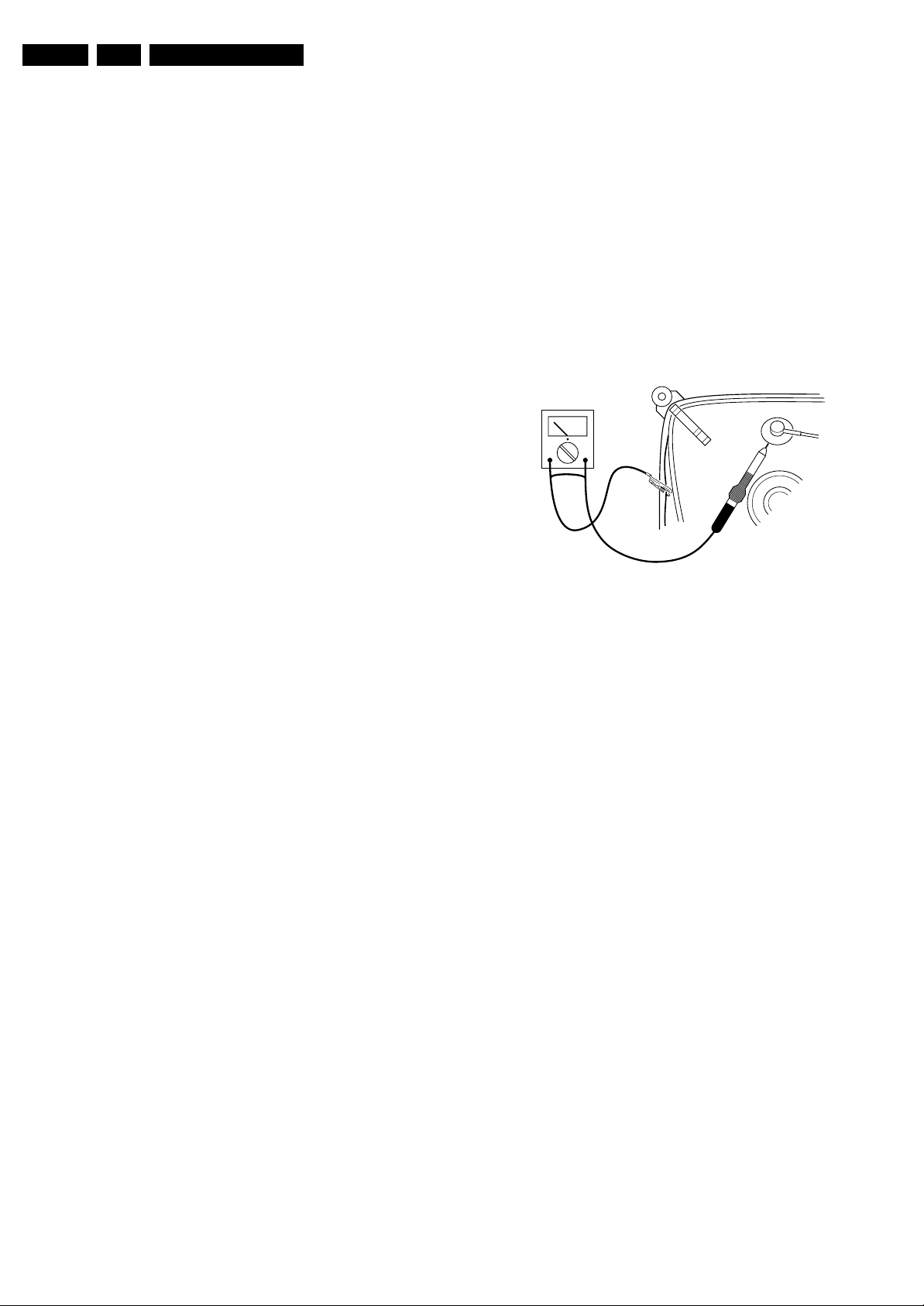
picture tube, use the method shown in figure “Discharge
picture tube”, to discharge the picture tube. Use a high
voltage probe and a multi-meter (position V
until the meter reading is 0 V (after approx. 30 s).
V
Figure 2-1 Discharge picture tube
• All ICs and many other semiconductors are susceptible to
electrostatic discharges (ESD w). Careless handling
during repair can reduce life drastically. Make sure that,
during repair, you are connected with the same potential as
the mass of the set by a wristband with resistance. Keep
components and tools also at this same potential. Available
ESD protection equipment:
– Complete kit ESD3 (small tablemat, wristband,
connection box, extension cable and earth cable) 4822
310 10671.
– Wristband tester 4822 344 13999.
• Be careful during measurements in the high voltage
section.
• Never replace modules or other components while the unit
is switched "on".
• When you align the set, use plastic rather than metal tools.
This will prevent any short circuits and prevents circuits
from becoming unstable.
2.4 Notes
2.4.1 General
• Measure the voltages and waveforms with regard to the
chassis (= tuner) ground (H), or hot ground (I), depending
on the tested area of circuitry. The voltages and waveforms
shown in the diagrams are indicative. Measure them in the
Service Default Mode (see chapter 5) with a color bar
signal and stereo sound (L: 3 kHz, R: 1 kHz unless stated
otherwise) and picture carrier at 475.25 MHz for PAL, or
61.25 MHz for NTSC (channel 3).
• Where necessary, measure the waveforms and voltages
with (D) and without (E) aerial signal. Measure the
voltages in the power supply section both in normal
operation (G) and in stand-by (F). These values are
indicated by means of the appropriate symbols.
• The semiconductors indicated in the circuit diagram and in
the parts lists, are interchangeable per position with the
). Discharge
DC
E_06532_007.eps
250304
Page 5
Safety Instructions, Warnings, and Notes
EN 5TC5.1L CB 2.
semiconductors in the unit, irrespective of the type
indication on these semiconductors.
• Manufactured under license from Dolby Laboratories.
“Dolby”, “Pro Logic” and the “double-D symbol”, are
trademarks of Dolby Laboratories.
2.4.2 Schematic Notes
• All resistor values are in ohms, and the value multiplier is
often used to indicate the decimal point location (e.g. 2K2
indicates 2.2 kohm).
• Resistor values with no multiplier may be indicated with
either an "E" or an "R" (e.g. 220E or 220R indicates 220
ohm).
• All capacitor values are given in micro-farads (μ= x10
nano-farads (n= x10
• Capacitor values may also use the value multiplier as the
decimal point indication (e.g. 2p2 indicates 2.2 pF).
• An "asterisk" (*) indicates component usage varies. Refer
to the diversity tables for the correct values.
• The correct component values are listed in the Spare Parts
List. Therefore, always check this list when there is any
doubt.
2.4.3 Rework on BGA (Ball Grid Array) ICs
General
Although (LF)BGA assembly yields are very high, there may
still be a requirement for component rework. By rework, we
mean the process of removing the component from the PWB
and replacing it with a new component. If an (LF)BGA is
removed from a PWB, the solder balls of the component are
deformed drastically so the removed (LF)BGA has to be
discarded.
-9
), or pico-farads (p= x10
-12
2.4.4 Lead-free Solder
Philips CE is producing lead-free sets (PBF) from 1.1.2005
onwards.
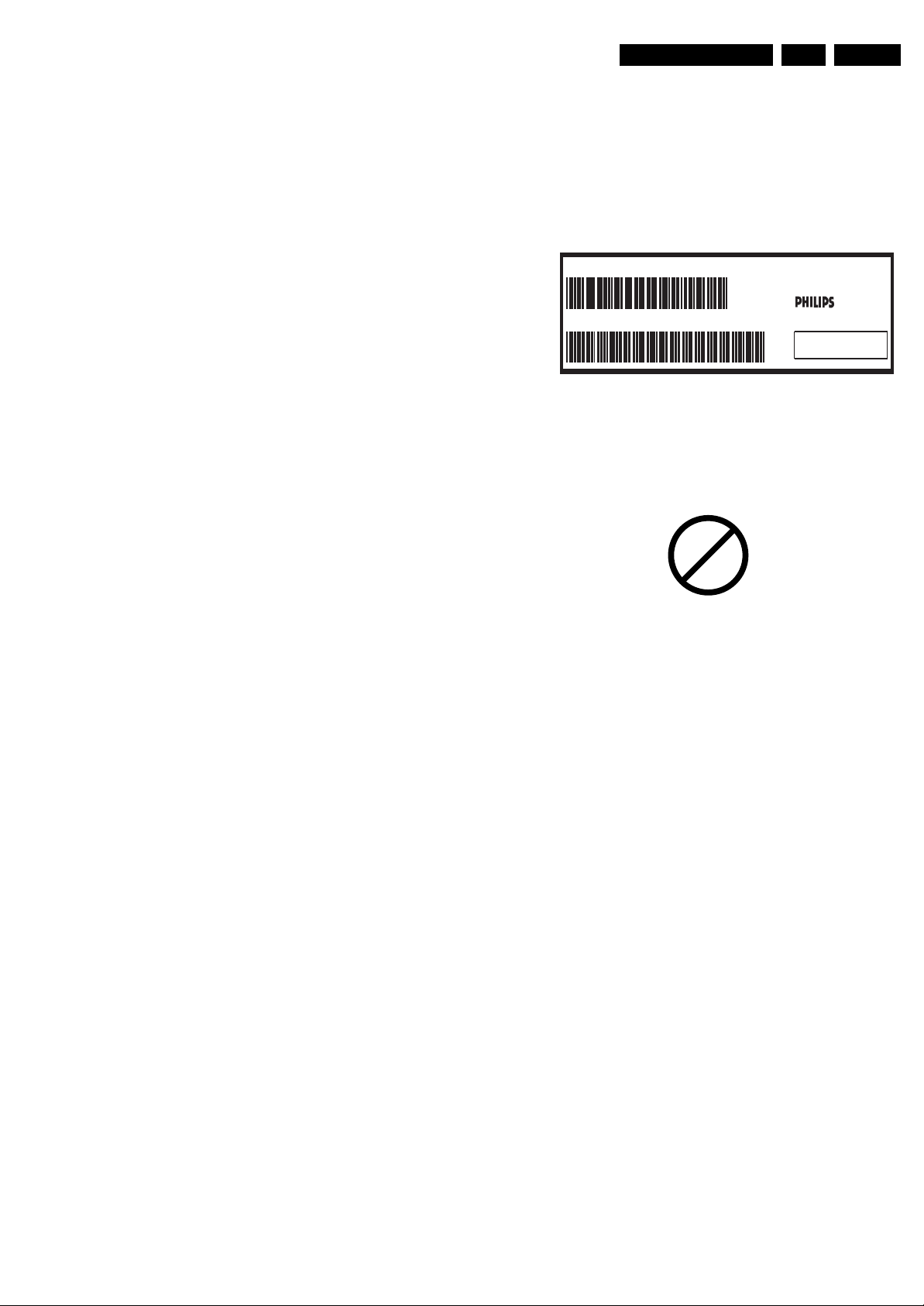
Identification: The bottom line of a type plate gives a 14-digit
serial number. Digits 5 and 6 refer to the production year, digits
7 and 8 refer to production week (in example below it is 1991
week 18).
MODEL :
-6
),
).
PROD.NO:
Regardless of the special lead-free logo (which is not always
indicated), one must treat all sets from this date onwards
according to the rules as described below.
32PF9968/10
AG 1A0617 000001
Figure 2-2 Serial number example
MADE IN BELGIUM
220-240V 50/60Hz
~
128W
VHF+S+H+UHF
BJ3.0E LA
S
E_06532_024.eps
130606
P
b
Figure 2-3 Lead-free logo
Device Removal
As is the case with any component that is being removed, it is
essential when removing an (LF)BGA, that the board, tracks,
solder lands, or surrounding components are not damaged. To
remove an (LF)BGA, the board must be uniformly heated to a
temperature close to the reflow soldering temperature. A
uniform temperature reduces the risk of warping the PWB.
To do this, we recommend that the board is heated until it is
certain that all the joints are molten. Then carefully pull the
component off the board with a vacuum nozzle. For the
appropriate temperature profiles, see the IC data sheet.
Area Preparation
When the component has been removed, the vacant IC area
must be cleaned before replacing the (LF)BGA.
Removing an IC often leaves varying amounts of solder on the
mounting lands. This excessive solder can be removed with
either a solder sucker or solder wick. The remaining flux can be
removed with a brush and cleaning agent.
After the board is properly cleaned and inspected, apply flux on
the solder lands and on the connection balls of the (LF)BGA.
Note: Do not apply solder paste, as this has been shown to
result in problems during re-soldering.
Device Replacement
The last step in the repair process is to solder the new
component on the board. Ideally, the (LF)BGA should be
aligned under a microscope or magnifying glass. If this is not
possible, try to align the (LF)BGA with any board markers.
So as not to damage neighboring components, it may be
necessary to reduce some temperatures and times.
More Information
For more information on how to handle BGA devices, visit this
URL: www.atyourservice.ce.philips.com (needs subscription,
not available for all regions). After login, select “Magazine”,
then go to “Repair downloads”. Here you will find Information
on how to deal with BGA-ICs.
Due to lead-free technology some rules have to be respected
by the workshop during a repair:
• Use only lead-free soldering tin Philips SAC305 with order
code 0622 149 00106. If lead-free solder paste is required,
please contact the manufacturer of your soldering
equipment. In general, use of solder paste within
workshops should be avoided because paste is not easy to
store and to handle.
• Use only adequate solder tools applicable for lead-free
soldering tin. The solder tool must be able:
– To reach a solder-tip temperature of at least 400°C.
– To stabilize the adjusted temperature at the solder-tip.
– To exchange solder-tips for different applications.
• Adjust your solder tool so that a temperature of around
360°C - 380°C is reached and stabilized at the solder joint.
Heating time of the solder-joint should not exceed ~ 4 sec.
Avoid temperatures above 400°C, otherwise wear-out of
tips will increase drastically and flux-fluid will be destroyed.
To avoid wear-out of tips, switch “off” unused equipment or
reduce heat.
• Mix of lead-free soldering tin/parts with leaded soldering
tin/parts is possible but PHILIPS recommends strongly to
avoid mixed regimes. If this cannot be avoided, carefully
clean the solder-joint from old tin and re-solder with new
tin.
• Use only original spare-parts listed in the Service-Manuals.
Not listed standard material (commodities) has to be
purchased at external companies.
• Special information for lead-free BGA ICs: these ICs will be
delivered in so-called "dry-packaging" to protect the IC
against moisture. This packaging may only be opened
shortly before it is used (soldered). Otherwise the body of
the IC gets "wet" inside and during the heating time the
structure of the IC will be destroyed due to high (steam-)
pressure inside the body. If the packaging was opened
before usage, the IC has to be heated up for some hours
(around 90°C) for drying (think of ESD-protection!).
Do not re-use BGAs at all!
Page 6

EN 6 TC5.1L CB3.
Directions for Use
• For sets produced before 1.1.2005, containing leaded
soldering tin and components, all needed spare parts will
be available till the end of the service period. For the repair
of such sets nothing changes.
In case of doubt whether the board is lead-free or not (or with
mixed technologies), you can use the following method:
• Always use the highest temperature to solder, when using
SAC305 (see also instructions below).
• De-solder thoroughly (clean solder joints to avoid mix of
two alloys).
Caution: For BGA-ICs, you must use the correct temperatureprofile, which is coupled to the 12NC. For an overview of these
profiles, visit the website www.atyourservice.ce.philips.com
(needs subscription, but is not available for all regions)
You will find this and more technical information within the
"Magazine", chapter "Repair downloads".
For additional questions please contact your local repair help
desk.
2.4.5 Alternative BOM identification
In September 2003, Philips CE introduced a change in the way
the serial number (or production number, see Figure 2-1) is
composed. From this date on, the third digit in the serial
number (example: AG2B0335000001) indicates the number of
the alternative BOM (Bill of Materials used for producing the
specific model of TV set). It is possible that the same TV model
on the market is produced with e.g. two different types of
displays, coming from two different O.E.M.s.
By looking at the third digit of the serial number, the service
technician can see if there is more than one type of B.O.M.
used in the production of the TV set he is working with. He can
then consult the At Your Service Web site, where he can type
in the Commercial Type Version Number of the TV set (e.g.
28PW9515/12), after which a screen will appear that gives
information about the number of alternative B.O.M.s used.
If the third digit of the serial number contains the number 1
(example: AG1B033500001), then there is only one B.O.M.
version of the TV set on the market. If the third digit is a 2
(example: AG2B0335000001), then there are two different
B.O.M.s. Information about this is important for ordering the
correct spare parts!
For the third digit, the numbers 1...9 and the characters A...Z
can be used, so in total: 9 plus 26 = 35 different B.O.M.s can
be indicated by the third digit of the serial number.
2.4.6 Practical Service Precautions
• It makes sense to avoid exposure to electrical shock.
While some sources are expected to have a possible
dangerous impact, others of quite high potential are of
limited current and are sometimes held in less regard.
• Always respect voltages. While some may not be
dangerous in themselves, they can cause unexpected
reactions that are best avoided. Before reaching into a
powered TV set, it is best to test the high voltage insulation.
It is easy to do, and is a good service precaution.
3. Directions for Use
You can download this information from the following websites:
http://www.philips.com/support
http://www.p4c.philips.com
4. Mechanical Instructions
See Chapter 10, Parts List.
Page 7
Service Modes, Error Codes, and Fault Finding
5. Service Modes, Error Codes, and Fault Finding
5.1 Trouble Shooting
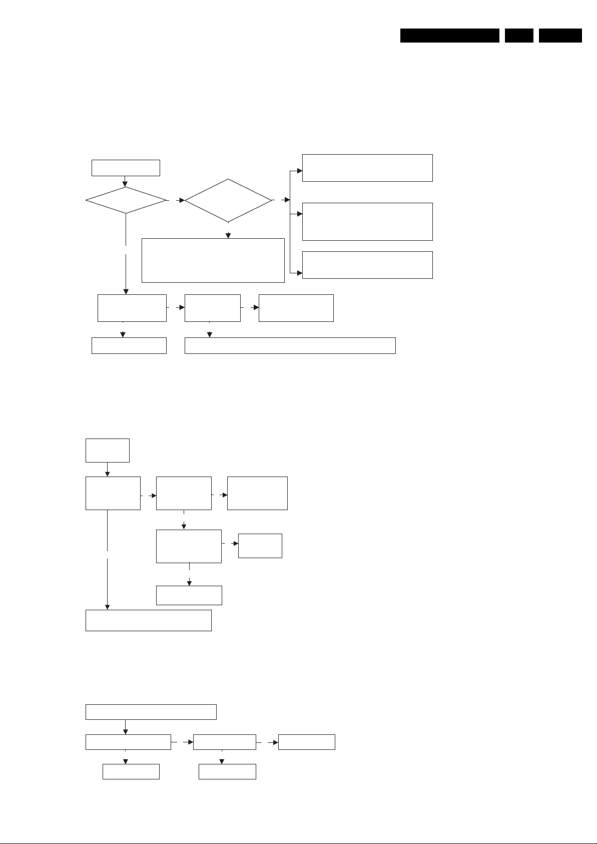
5.1.1 Can not Power On
EN 7TC5.1L CB 5.
Can not Power On
Fuse OK?
(1) Check if B+ shorted to earth.
(2) To check whether D822 and R821 are
N
(3) To check whether D823 and R823 are
Is it IC801 Pin 1
shorted to earth?
Y
Check/Replace IC801
5.1.2 No Raster, Sound OK
No Raster
Sound OK
Check B+,
Y Y
turnoff.
turnoff. And whether C836 shorted.
+12V, Ok?
N
Is DB801 OK?
NN
Y
Check the components such as C801, C802, C806, C807 and C815
Is power supply for IC101 correct?
If not, check Q820, Q821, Q007, Q008,
D001
Check Horizontal Scan circuit:
Check H-Vcc and H-out of IC 101
Check Q401, T401 and Q411
Check standby circuit: Check Pin64 of
IC101, Check Q825, Q824, Q823, Q822.
Replace DB801
Figure 5-1 Can not Power On
G_16340_004.eps
100306
Is the power
supply of Q401
and Q411 ok?
N
To check whether R404, C401, T401,
Q401, R422 are ok?
Check Pin 13
(H-OUT) voltage
ok?
Y
Is there any shorted
in the scan part of
the circuit?
Change IC101
Y
N
Y
N
5.1.3 Raster OK, Sound OK, No TV/AV picture
Raster OK, Sound OK, No TV/AV picture
Check whether Q917 is
ok?
N
Replace Q917
Y Y
Replace C238
N
Check each
output voltage of
FBT
Change the
shorted part.
G_16340_005.eps
100306
Figure 5-2 No Raster, Sound OK
Change IC901 Check C238, ok?
G_16340_008.eps
100306
Figure 5-3 Raster OK, Sound OK, No TV/AV picture
Page 8
EN 8 TC5.1L CB5.
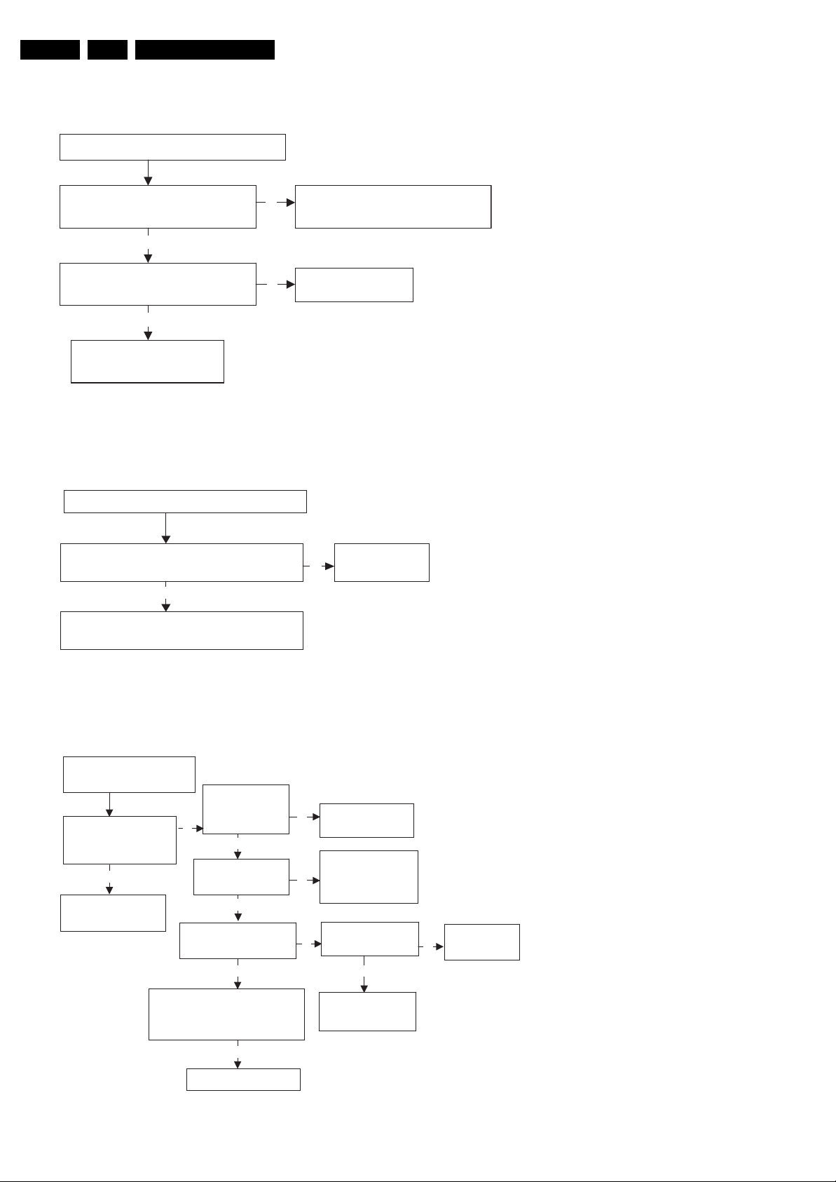
5.1.4 Raster OK, Sound OK, No AV picture
Raster OK, Sound OK, No AV picture
Service Modes, Error Codes, and Fault Finding
Is the signal waveform at Pin 12 and
Pin 14 of IC901 right?
Y
Check Q917, Q918, Q919, ok?
N
Replace the fail component.
5.1.5 Raster OK, Sound OK, No TV picture
Raster OK, Sound OK, No TV picture
Is the signal waveform at Pin 15 of IC901
right?
N
To check whether R903, C903, R902
N
and R905, C908, R908 are ok?
Replace IC901
Y
G_16340_006.eps
100306
Figure 5-4 Raster OK, Sound OK, No AV picture
Replace
IC901
Y
Check R234, Q204, R235, C229
5.1.6 No picture, dense noise dots
No picture, dense noise
dots
Is the antenna feed line
or the adapter broken?
Y
Handing the antenna
fault
N
Is the signal at Pin SCL,
SDA of tuner ok?
Check signal at P5, P57, P58,
P59, and P60 of IC101 and
replace the abnormal relative
circuit
Figure 5-5 Raster OK, Sound OK, No TV picture
Is the signal at
Pin41, Pin42 of
IC101 ok?
N
Is the signal at IF
pin of the tuner ok?
N
N N
Y
Check/Replace
Y
IC101
Check the relative
circuit of Q101,
Y
Z141 etc
Is the supply
voltage of tuner ok?
Y
Check/Replace
IC201, IC202,
D101.
G_16340_007.eps
100306
Check/Replace
Tuner
Y
Check EEPROM
G_16340_009.eps
Figure 5-6 No picture, dense noise dots
100306
Page 9
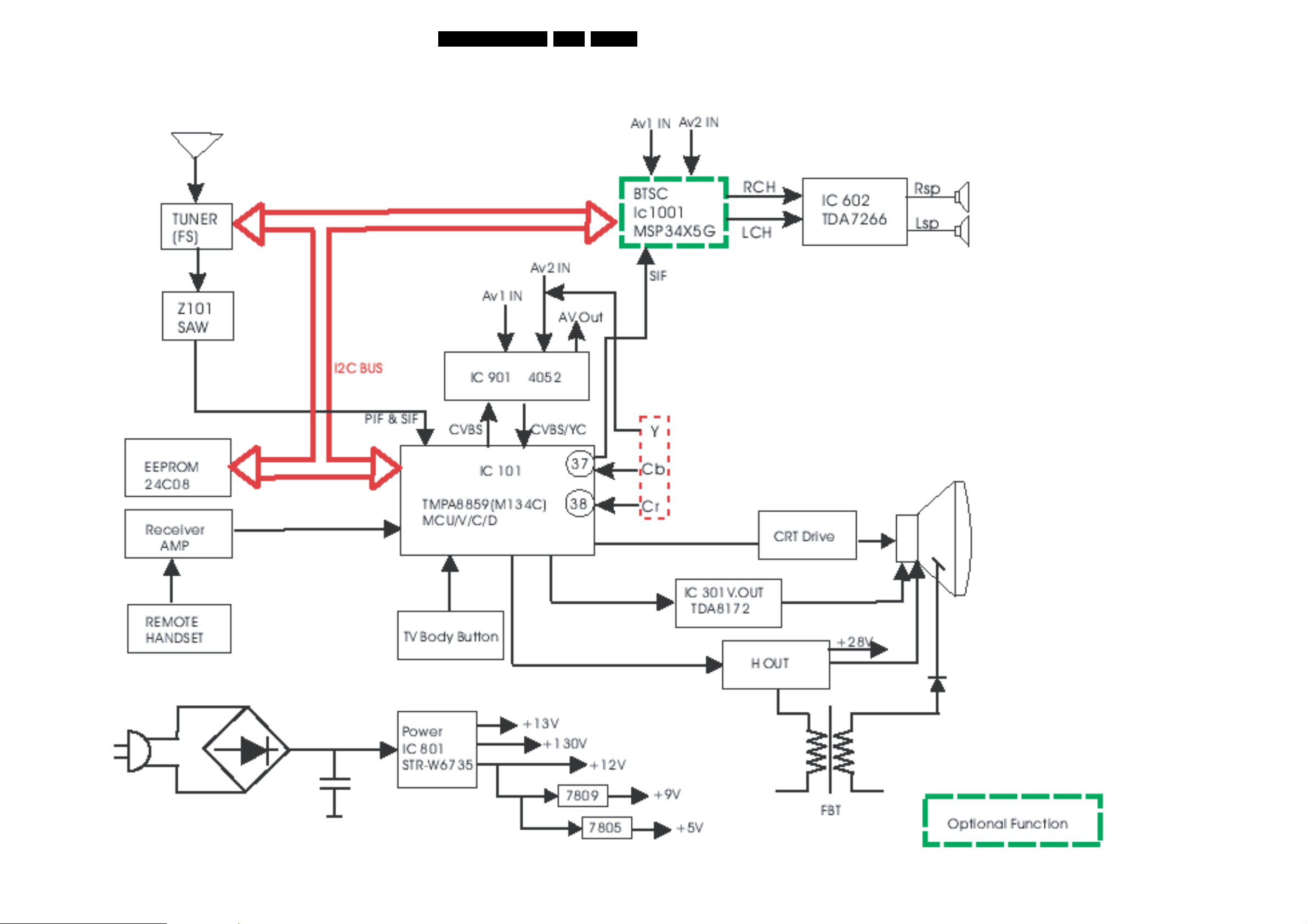
Block Diagrams, Test Point Overviews, and Waveforms
6. Block Diagrams, Test Point Overviews, and Waveforms
Chassis Block Diagram
EN 9TC5.1L CB 6.
* /44 sets use STR-W6756
H_17510_009.eps
021107
Page 10
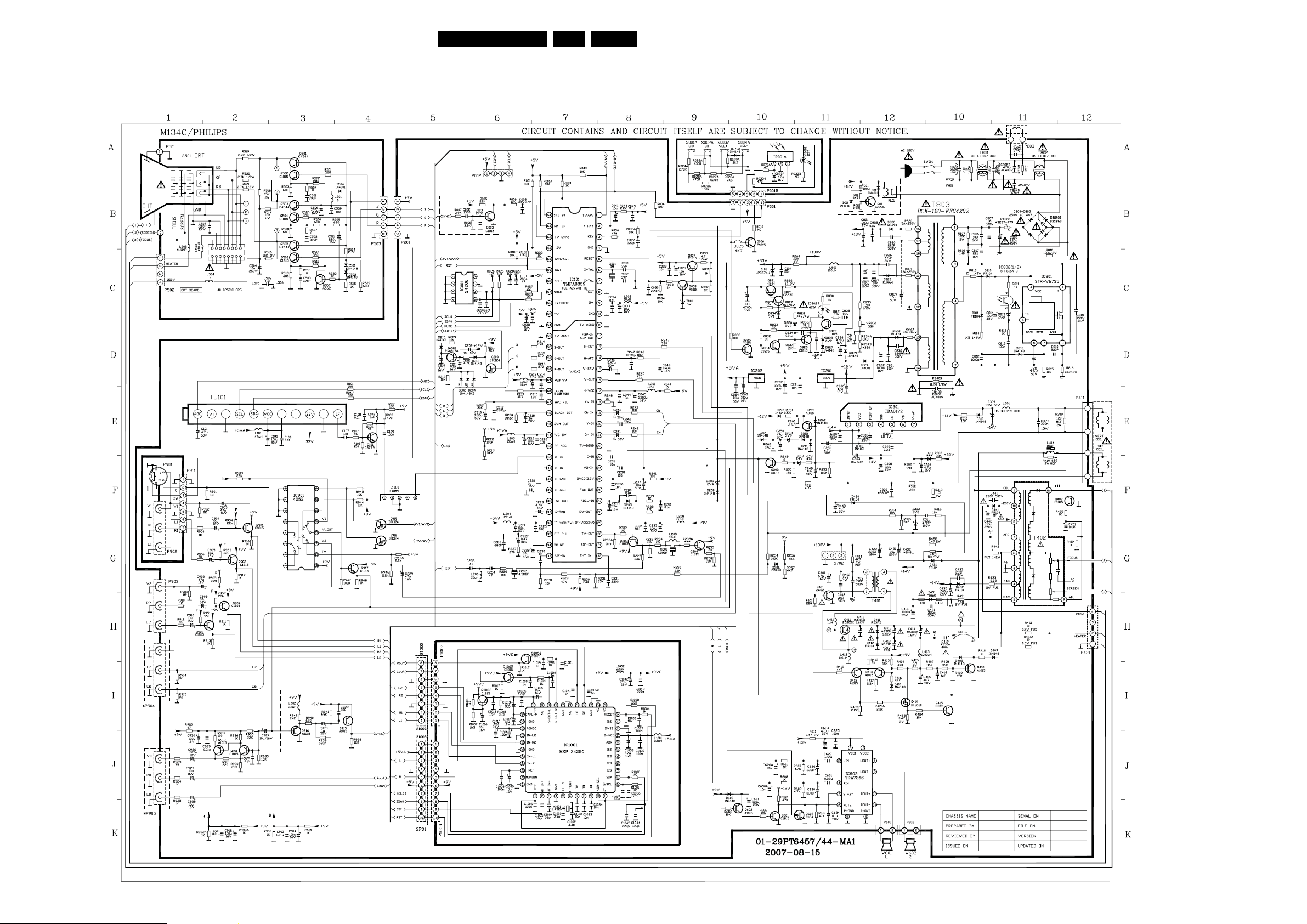
Circuit Diagrams and CBA Layouts
7. Circuit Diagrams and CBA Layouts
Main Board 01-29PT6457/44-MA1
EN 10TC5.1L CB 7.
H_17510_001.eps
021107
Page 11
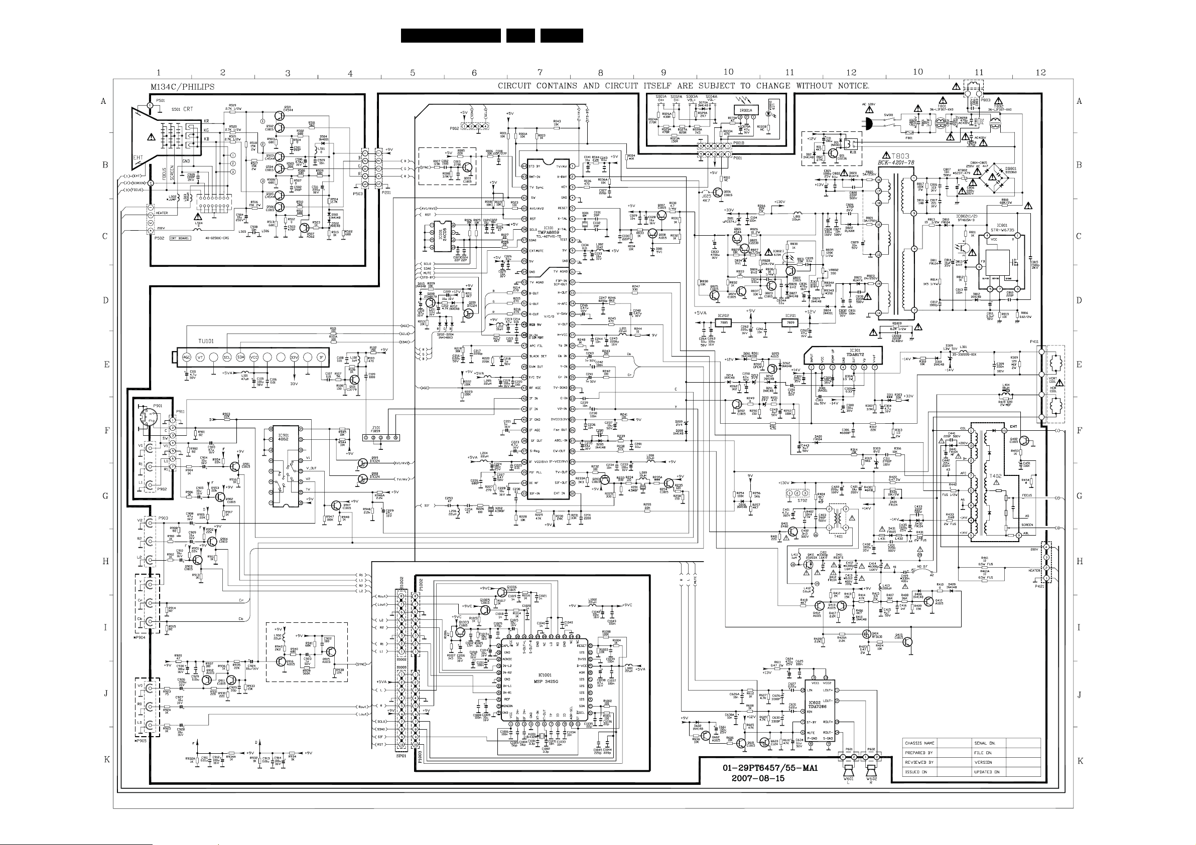
Circuit Diagrams and CBA Layouts
Main Board 01-29PT6457/55-MA1
EN 11TC5.1L CB 7.
H_17510_004.eps
021107
Page 12
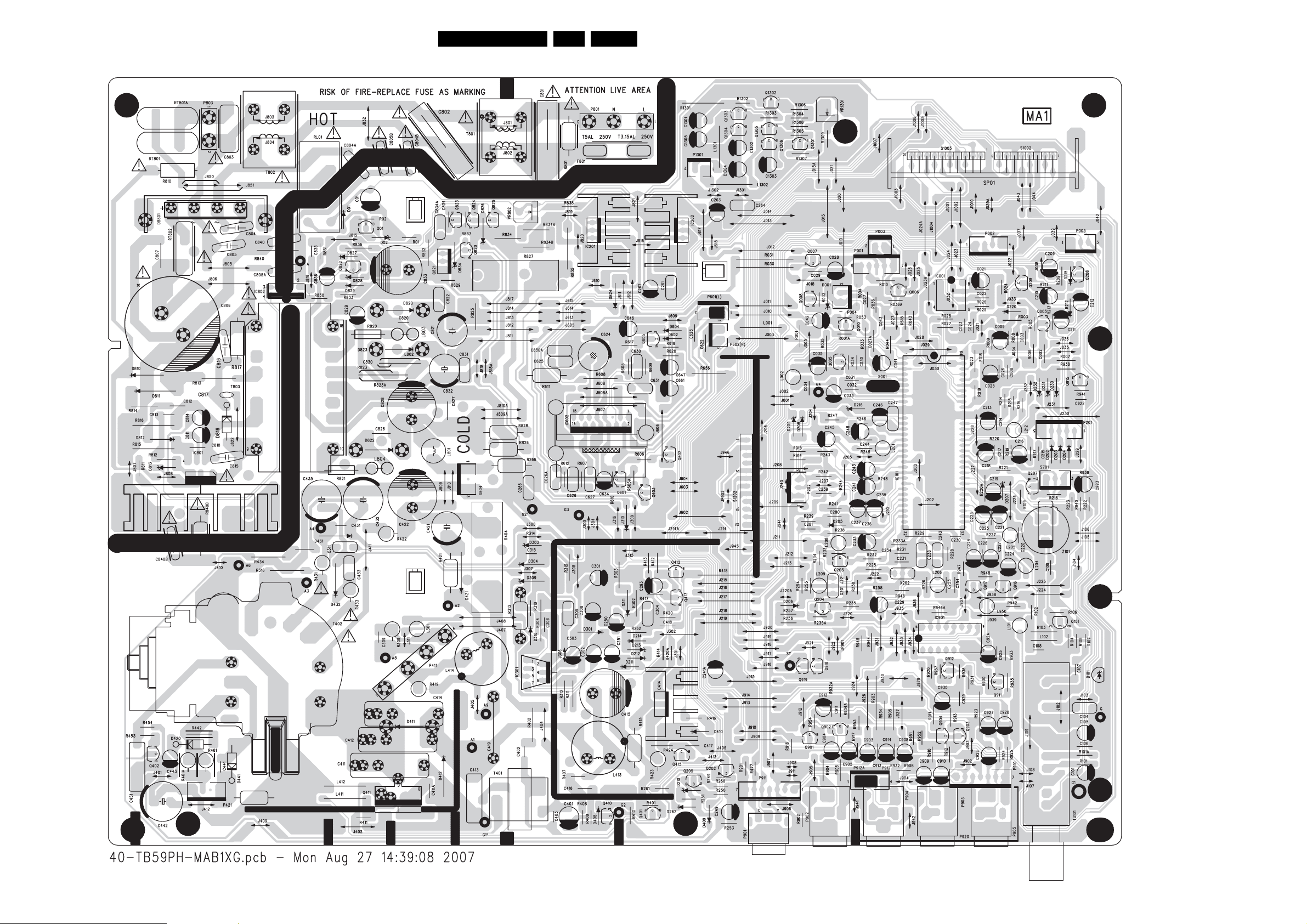
Circuit Diagrams and CBA Layouts
Layout Main Board 40-TB59PH-MAB1XG (Top Side)
EN 12TC5.1L CB 7.
H_17510_002.eps
021107
Page 13
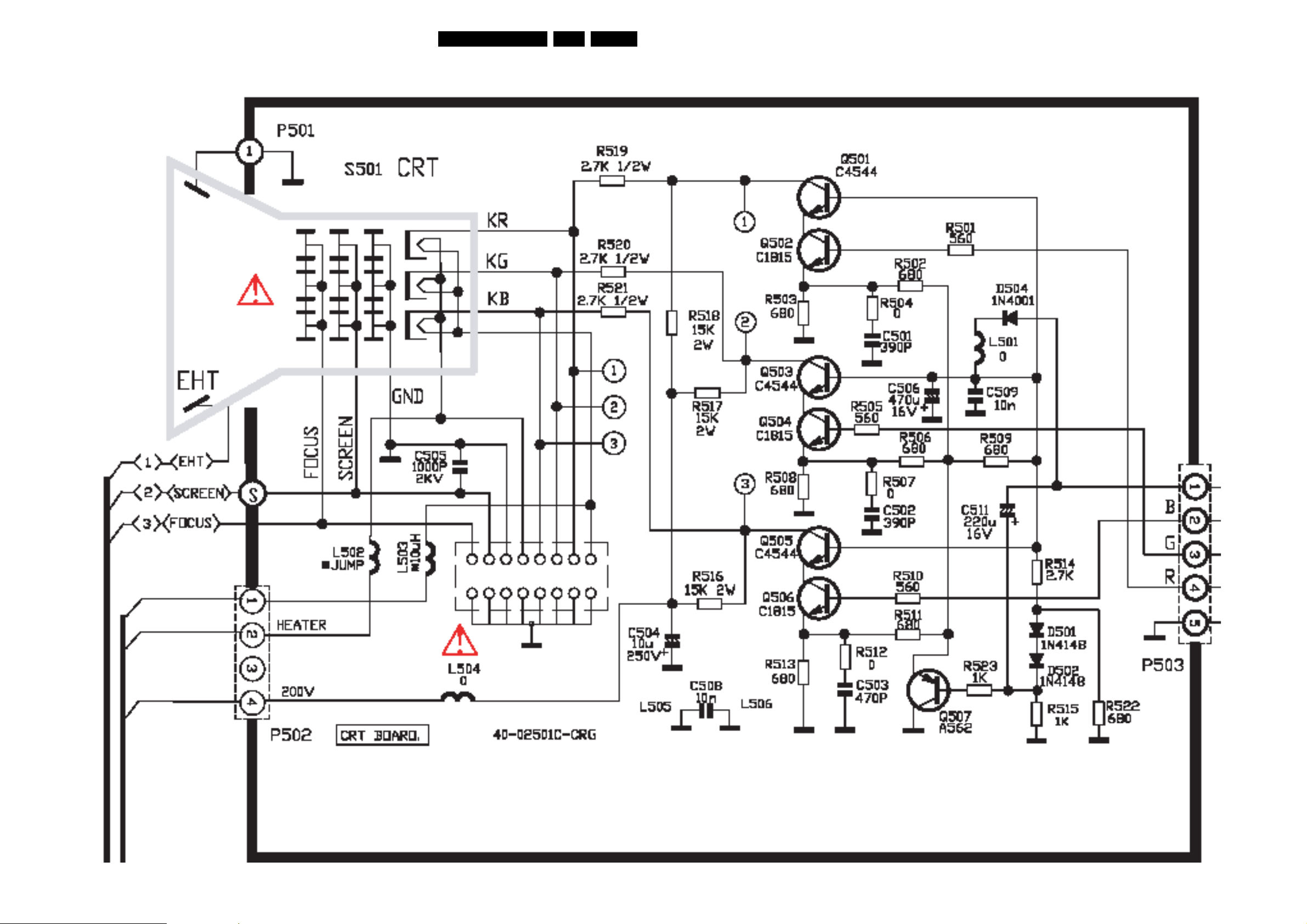
CRT Panel
Circuit Diagrams and CBA Layouts
EN 13TC5.1L CB 7.
G_16340_014.eps
100306
Page 14
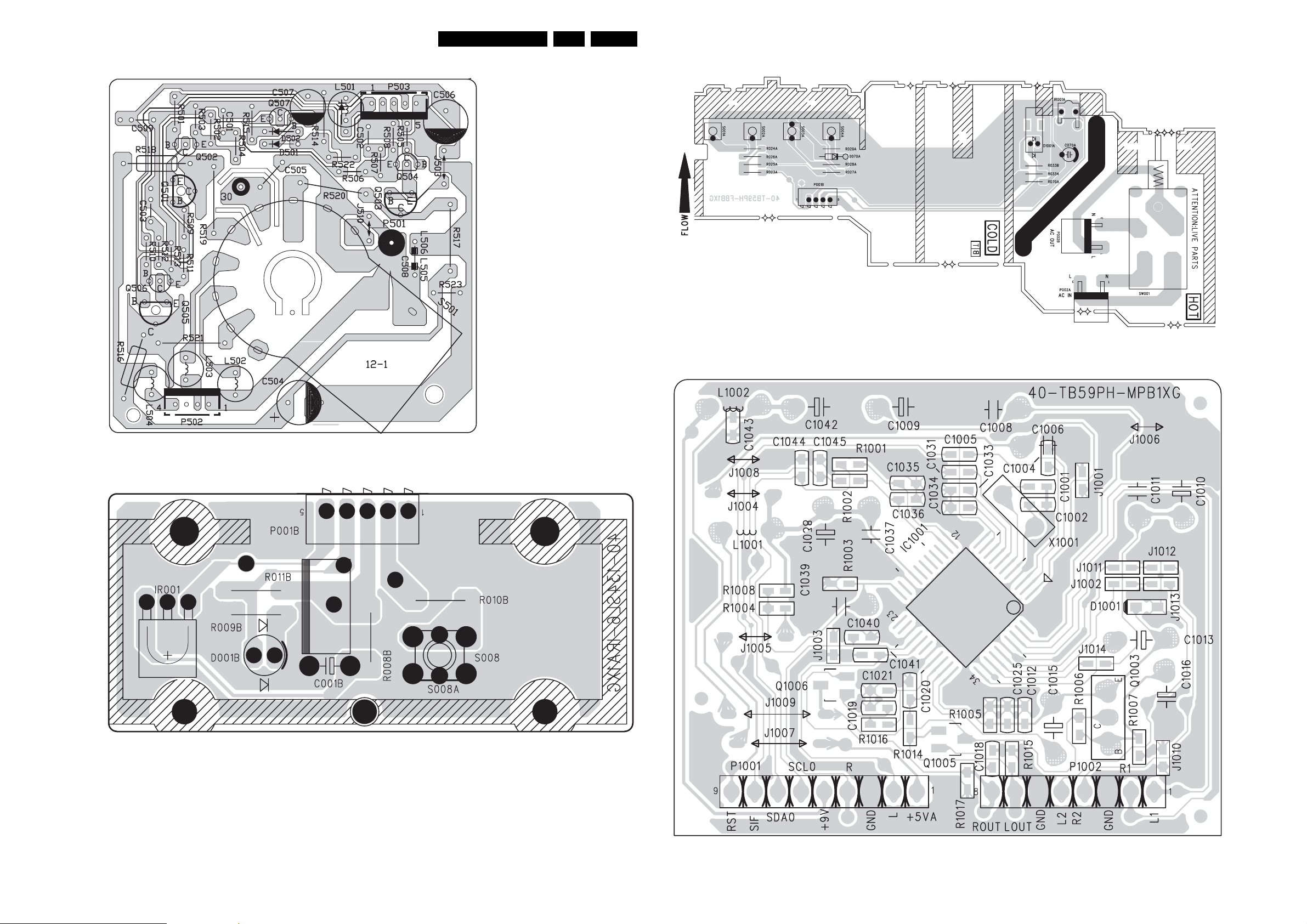
Circuit Diagrams and CBA Layouts
EN 14TC5.1L CB 7.
Layout CRT Panel
Layout Front IR Panel 40-TB59PH-FBB1XG
Layout BTSC Panel 40-TB59PH-MPB1XG
H_17510_007.eps
021107
Side I/O Panel 40-TB59PH-SIA1XG
H_17510_003.eps
021107
H_17480_005.eps
041007
H_17510_008.eps
021107
Page 15
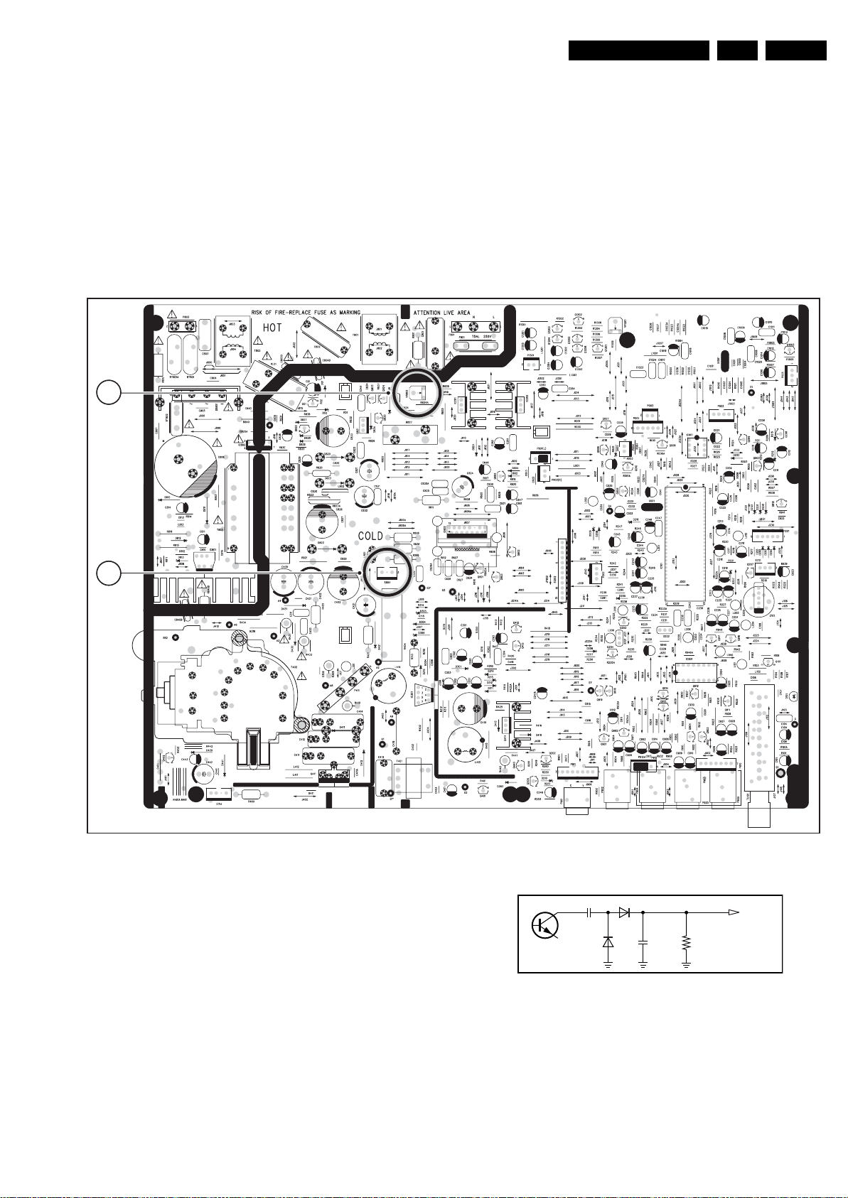
8. Alignments
Alignments
EN 15TC5.1L CB 8.
8.1 How to Put the Set into Factory Mode
• Press the “D-MODE” button on the remote control.
• Press the “OK” button on the remote control.
• Press the “CH+” or the “CH-” button to select the parameter
you want to adjust.
• Press the “VOL+” or the “VOL-” button to adjust the
selected parameter.
• To put the new values into the memory, leave the factory
mode with the “D_MODE” button on the remote control.
22
8.2 Adjustment of the B+ (BAT) voltage
1. Apply the Philips standard test pattern to the RF input.
2. Connect a DC voltmeter (range >200 V) to pins 1 (GND)
and 3 (+) of S804 [1].
3. Adjust potentiometer VR802 [2] in STANDARD mode in
such a way the voltage reading is 130 +/- 0.5 V.
21
8.3 RF AGC Alignment:
1. Connect a test circuit as depicted in figure “Test circuit”.
2. Apply an 8-scale gray signal (80 dBμV).
3. Adjust the AGC data until the output of the test circuit
becomes 0.4 V (p-p) ±0.05 V.
4. Change the 8-scale gray signal to 60 dBμV.
5. The shown value of CRO should be the same as while
receiving the 80 dBμV signal. If not, repeat step 3 and 4
until the results for 60 dBμV and 80 dBμV input signal are
the same.
Figure 8-1 Test pin & potentiometer position
Q101
D2
C1
1N60
33pF
D1
C2
1N60
100pFR1100k
Figure 8-2 Test circuit
TO CRO
H_17480_007.eps
050707
H_17480_006.eps
051007
Page 16

EN 16 TC5.1L CB8.
Alignments
8.4 Screen & Focus Voltage Adjustment
1. Apply the test pattern signal in normal status.
2. Enter the Factory mode
3. Press the "TV/AV" button to stop the vertical scan (Note:
the RC/GC/BC is preset to 80, GD/BD to 40)
4. Adjust the SCREEN potentiometer on the line output
transformer in such a way the horizontal line is just visible
on the screen.
5. Measure the VG2 voltage with a High Voltage Meter and a
High Voltage Test stick (1000:1). The VG2 voltage should
be 675 ±50 V.
6. Turn on the vertical output, and adjust the "FOCUS"
potentiometer on the line output transformer in such a way
the focus is maximized. The “FOCUS” voltage should be
within the range of 7 - 8.0 kV.
8.5 White Balance Adjustment (NORMAL)
Normal color temperature adjustment.
1. In Rich Status, choose a
AV input (Color Temperature = normal).
2. Adjust Brightness & Contrast until at the grey side Y = 5 ±1
Nits and at the white side Y = 85 ±10 Nits.
3. Use color analyzer to measure the grey side of the screen.
By adjusting the value of RC, GC and BC, set the reading
of the color analyzer x = 274 ±8 and y = 280 ±8.
4. Use color analyzer to measure the white side of the screen.
By adjusting the GD and BD, set the reading of the color
analyzer to x = 274 ±8 and y = 280 ±8.
5. Repeat steps 2 to 4 until the reading of the color analyzer
is correct on both grey and white picture.
Cool color temperature adjustment.
1. In Rich status, choose a
AV input (Color Temperature = cool).
2. Adjust RC-C, GC-C, BC-C, GD-C and BD-C as described
in 2, 3, 4 and 5 of the “Normal color temperature
adjustment” procedure until you have reached a reading on
the color analyzer of x = 263 ±8 and y = 265 ±8.
Warm color temperature adjustment.
1. In Rich status, choose a
AV input (Color Temperature = warm).
2. Adjust RC-W, GC-W, BC-W, GD-W and BD-W as
described in 2, 3, 4 and 5 of the “Normal color temperature
adjustment” procedure until you have reached a reading on
the color analyzer of x = 291 ±8 and y = 300 ±8.
CVI color temperature adjustment.
1. In Rich status, choose a
CVI input (Color Temperature = normal).
2. Adjust YUVRC, YUVGC, YUVBC, YUVGD and YUVBD as
described in 2, 3, 4 and 5 of the “Normal color temperature
adjustment” procedure until you have reached a reading on
the color analyzer of x = 274 ±8 and y = 280 ±8.
1
/2 grey and 1/2 white pattern from
1
/2 grey and 1/2 white pattern from
1
/2 grey and 1/2 white pattern from
1
/2 grey and 1/2 white pattern from
8.7 Picture Geometry Adjustment
1. Apply the Philips NTSC standard testing pattern in normal
status.
2. Then enter menu 3.
3. Adjust the following data to get the minimum distortion:
a. HPOS6 (Horizontal Centre).
b. PARA6 (Level).
c. TRAP6 (Trapezium).
d. HSIZE6 (Horizontal Size).
e. CNRT6 (Top).
f. CNRB6 (Bottom).
4. Apply the Philips NTSC standard testing pattern in normal
status.
5. Enter menu 3.
6. Adjust the following data to get the minimum distortion:
a. HIGH6 (Height).
b. VP60 (Vertical Center).
c. VLIN6 (Linearity).
d. VSC6 (Vertical-S Correction).
7. Apply the Philips PAL standard testing pattern in normal
status.
8. Then enter menu 3.
9. Adjust the following data to get the minimum distortion:
a. HPOS6 (Horizontal Centre).
b. PARA6 (Level).
c. TRAP6 (Trapezium).
d. HSIZE6 (Horizontal Size).
e. CNRT6 (Top).
f. CNRB6 (Bottom).
10. Apply the Philips PAL standard testing pattern in normal
status.
11. Enter menu 2.
12. Adjust the following data to get the minimum distortion:
a. HIGH5 (Height).
b. VP50 (Vertical Center).
c. VLIN5 (Linearity).
d. VSC5 (Vertical-S Correction).
8.8 The Peak White Adjustment
In Rich status and Color Temperature = Normal, apply the peak
white signal with a 14x14 cm window to the AV input. Enter
factory alignment menu 5, select SCNT to adjust the subcontrast until the spec of the window is 285 ±15 Nits.
8.9 Initialization
Put the set into “Factory Mode” (see “How to Put the Set into
Factory Mode”, the first item of this chapter). Press the
"SOUND" button, the screen displays "WAIT". When the
screen displays "OK", the initialization is finished.
8.6 Adjustment of Sub-brightness
1. In Rich & Normal status, apply standard grey & white
pattern via RF (NTSC-M).
2. Test the brightness of grey side of the picture to meet
BRTS 17 - 21 Nits.
Page 17
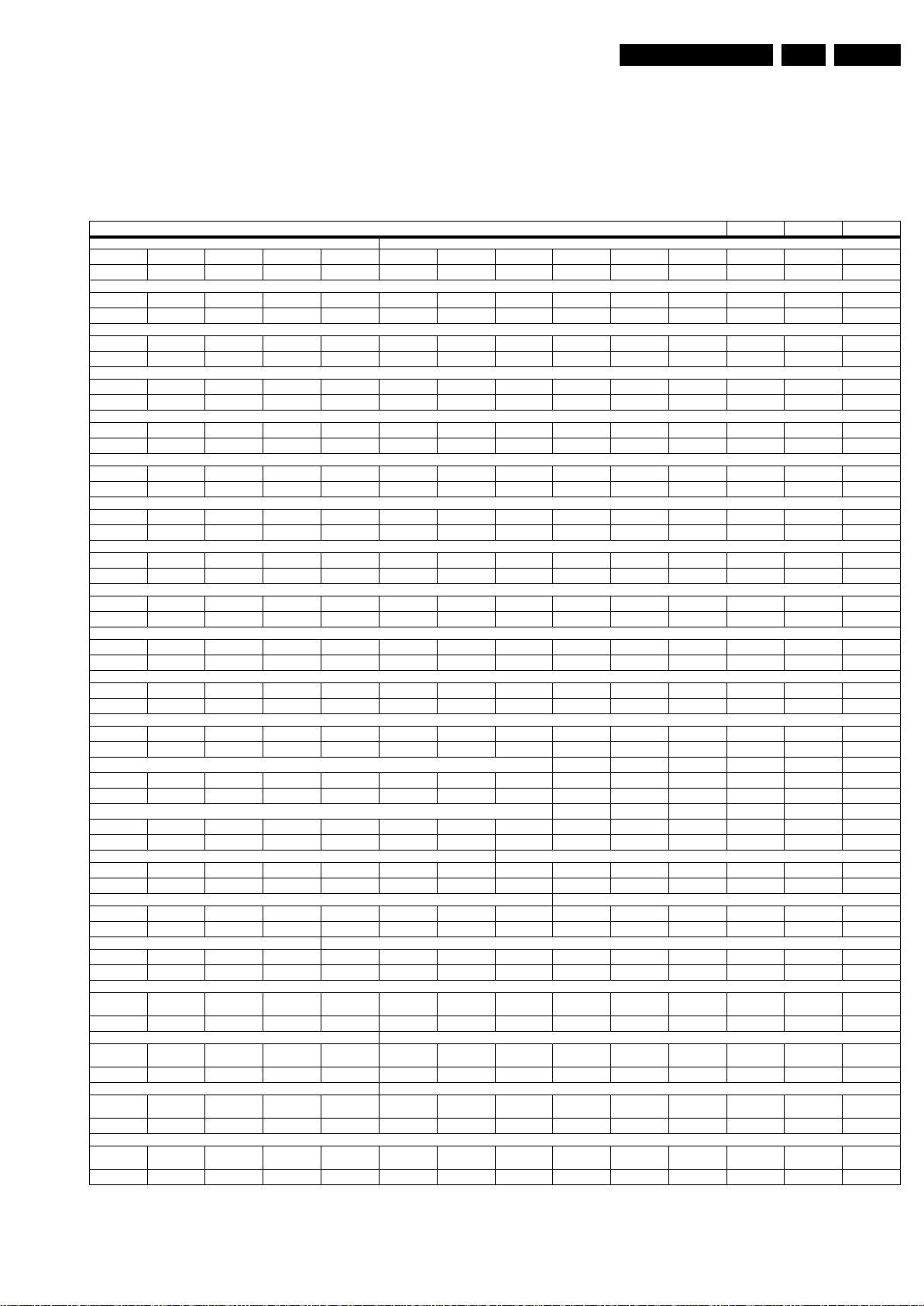
8.10 EEPROM Data:
Note: although all items are adjustable, we only recommend to
adjust the items with an asterisk (*). The other items are
adjustable as well, but we strongly discourage adjusting them.
Table 8-1 EEPROM Data
Alignments
EN 17TC5.1L CB 8.
FAC 01 FAC 02
EEPROM data
RC* GC* BC* GD* BD* HIGH5 VP50 VLIN5 VSC5 VBLK5 VCEN5
80 80 80 40 40 1C 03 0C 0C 00 27
FAC 02
HIGH6* VP60* VLIN6* VSC6* VBLK6 VCEN6
1C 03 0A 0C 00 29
FAC 03
HPOS5 PARA5 TRAP5 HSIZE5 CNRT5 CNRB5 VEHT5 HEHT5
08 22 29 1A 06 09 03 03
FAC 03
HPOS6* PARA6* TRAP6* HSIZE6* CNRT6* CNRB6* VEHT6 HEHT6
0C 1F 21 1B 09 0A 03 03
FAC 04
CNTX CNTN BRTX BRTN COLX COLN TNTX TNTN
7F 08 27 42 35 00 28 28
FAC 05
BRTC* COLC COLP SCOL SCNT CNTC TNTCT TNTCV
40 2C 00 04 04 67 40 40
FAC 06
ST3 SV3 SV4 SVD ASSH SHPX SHPN
20 20 19 19 07 3F 3F
FAC 07
MOD1 MOD2 MOD3 OPT OPTM1 OPTM2 HDCNT HSTOP
20 B0 60 3F C0 02 00 FF
FAC 08
RFAGC* BRTS OSD OSDF CCD OSD CCD OSDF TXCN RGCN
25 00 21 53 4A 65 1F 16
FAC 09
V01 V05 V10 V25 V50 V75 V90 V100
46 4F 52 58 6A 6B 6C 6D
FAC 10
MODE4 MODE5 MODE6 MODE7 MODE8 MODE9
12 0B 1F 95 8D 02
FAC 11
MPB-STR MPB-HMC MPB-HP MPB-LP MPB-LIM SUB-FRE SUB-HP VOL-MAI
43 0D 07 11 00 28 02 01
FAC 12
SVM SVM1 OSD2 OSDF2 PYNX PYNN PYXS PYNS
05 05 20 64 28 18 22 10
FAC 13
CLTM CLVO CLVS ABL DCBS FLG0 FLG1
44 43 43 27 14 82 0D
FAC 14 FAC 15
HAFC AGCC NOIS ONTM NSHP PVLVL PLMT RC-C GC-C BC-C GD-C
09 1C 01 08 1A 80 80 00 FF FC 01
FAC 16 FAC 17
RC-W GC-W BC-W GD-W BD-W YUVGC YUVBC YUVRC D-COL D-BRI D-CON D-SHP
00 01 05 FB EE FF 02 00 26 2D 64 5A
FAC 18 FAC 19
S-COL S-BRI S-CON S-SHP M-COL M-BRI M-CON M-SHP
1C 28 49 49 1E 2E 52 50
FAC 20
SEGPOINT1
173 407 01 02 08 06 05 00 00
FAC 21 FAC 22
T-Hz120 BAS
28 50 0C 0C 0C 3C 3E 0C 0C 0C
FAC 23 FAC 24
B-Hz120BAS
19 2B 0C 0C 0C 00 05 00 46 00
FAC 25
VOLMAX CURTCEN GATE VOL-OUT COLC-CVI COLX-CVI COLN-CVI SDET-
32 A5 2A 73 1E 20 00 04
SEGPOINT2
T-Hz500 TRE
B-Hz500TRE
DATA-VL DATA-VH DATA-UF SPE-POS1 SPE-DATA1 SENSI-ON SENSI -OFF
T-Hz1K5 T-Hz5K T-Hz10K C-Hz120-
B-Hz1K5 B-Hz5K B-Hz10K COMB1 COMB2 COMB3 AV GAIN OPTM3
BAS
C-Hz500 TRE
C-Hz1K5 C-Hz1K C-Hz10K
TIMER
BD-C YUVGD YUVBD
0C FD 00
Page 18
EN 18 TC5.1L CB9.
Circuit Descriptions, Abbreviation List, and IC Data Sheets
9. Circuit Descriptions, Abbreviation List, and IC Data Sheets
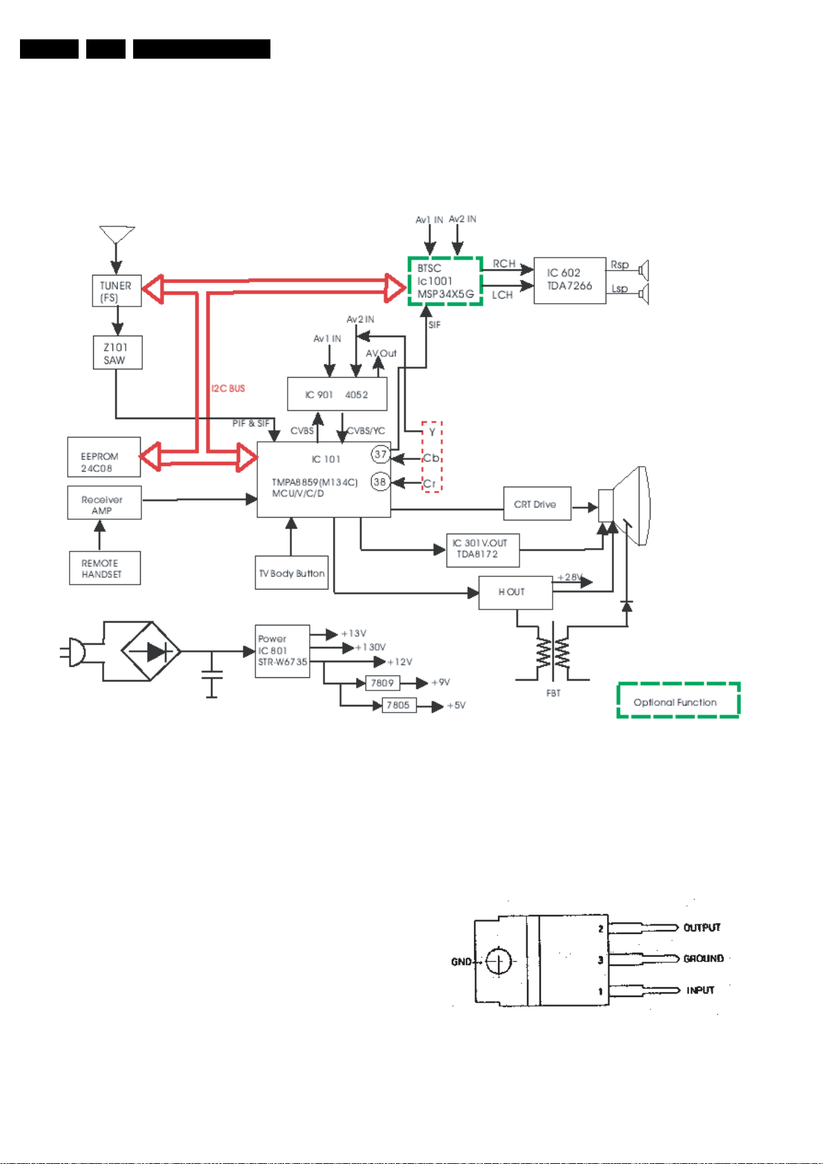
9.1 Brief Introduction of the Chassis
9.1.1 Chassis block diagram
* /44 sets use STR-W6756
9.1.2 Power Supply Section
This section mainly consists of
• IC STR-W6735 (/44 sets use STR-W6756) (IC801).
• Transformer (T803).
• Bridge rectifier (DB801).
• Accessory circuits.
The supply voltage for this chassis should be AC 110V. The
allowed voltage range is 90V to 140V, the frequency range is
50/60Hz.
The AC power with high/low frequency interference goes
through an RC filter, consisting of C801, T801, C802, R801,
and T802. The filter removes the high/low frequency
interference. Then DB801 transforms the AC power to DC
power. T803 and IC 801 work in standby state. T803 will
provide a power voltage to IC101. IC101 scans for the "KEY IN"
signal (Pin 3 of IC101) from the ON/OFF switch on the
keyboard. If "KEY IN" = "power on" signal, pin 64 (IC101) will
generate a signal to drive the photo coupler (IC8021). It acts as
a feed back circuit (feed back to Pin 6 of IC801) for controlling
IC801 to adjust MOSFET.
Transformer T803 provides the following voltages:
• +13V voltage from Pin16.
Figure 9-1 Chassis block diagram
• +130V (B+) voltage from Pin1.
• +12V from Pin 15.
• Pin 15 is also connected to two Positive Voltage
The picture below shows IC201 and IC202:
H_17510_009.eps
021107
Regulators (IC201, IC202) in-series. The outputs of these
regulators are +9V and +5V respectively.
G_16340_022.eps
100306
Figure 9-2 IC 201/202
Page 19
Circuit Descriptions, Abbreviation List, and IC Data Sheets
6
9.1.3 Tuning Section
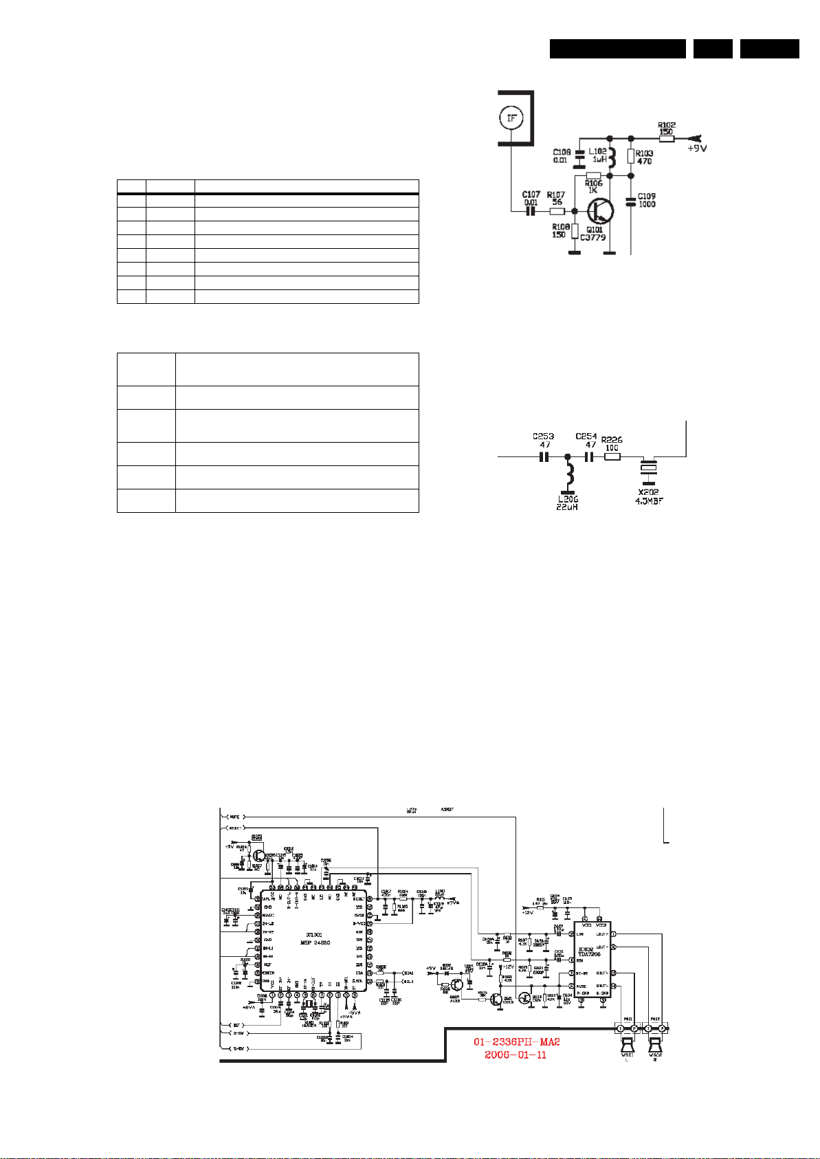
This section mainly consists of the tuner (TU101), the IF preamplifier circuit and the SAWFILTER.
Table 9-1 Tuning section 1
Pin Symbol Description
1 AGC Auto gain control
2 AS I2C bus address select
3 SCL I2C bus serial clock
4 SDA I2C bus serial data
5
6 BP Supply voltage tuner section +5V
7 BT Supply voltage tuning section +31V
8 IF Intermediate frequency out
Table 9-2 Short specification of the tuner
Receiving
Channel
Receiving
System
Intermediate
Frequency
Antenna Input
Impedance
Output Impedance
Band changeover system
VHF LOW BAND: CH2~B(55.25~127.25MHz)
VHF HIGH BAND: CH C~CH W+11(133.25~361.25MHz)
CH W+12~69(367.25~801.25MHz)
NTSC
Picture carrier: 47.74MHz
Colour carrier: 42.17MHz
Sound carrier: 41.25MHz
Unbalanced 75Ohms
Unbalanced 75Ohms
Digital change by PLL IC
G_16340_023.eps
10030
Figure 9-3 Pre-amplifier circuit
9.1.4 Sound Process Section
The SIF signal is sent out together with the TV signal from
Pin30 of IC101. It passes through Q203, R225. X202 and a
High-pass filter (consisting of C254, L206, C253) filters out the
video signal and low frequency interference.
G_16340_024.eps
100306
EN 19TC5.1L CB 9.
From Pin58 of IC101 the I2C bus clock signal goes to the tuner.
The tuner works during the clock time. IC101 will send out a
data signal from Pin57 to control the tuner's working state by
controlling the +33V voltage. +33V is provided from Pin10 of
T803. That voltage is put into the tuner at Pin7. A circuit inside
the tuner transforms +33V into a voltage between 0 and +33V
(as a function of the data, sent by IC101).
The AGC signal is a close loop control voltage that keeps the
amplitude of the signal constant.
Output of tuner is the Intermediate Frequency signal (IF signal).
The IF signal will pass pre-amplifier circuit (refer to the picture
below). The amplified IF signal passes the SAW filter and is
then sent to IC101 Pin41/42.
IC101 creates a CVBS signal and sends it out from Pin30.
CVBS will be selected by IC901, and then pass from Pin13 of
IC901 to Pin20/24 if IC101. IC101 will demodulate the CVBS
signal into an R, G, B signal. Next IC101 will send this R, G, B
signal from Pin50/51/52 to the CRT board.
Figure 9-4 Sound process section 1
SIF will be finally sent into Pin2 of IC1001. An analog automatic
gain control circuit (AGC) allows a wide range of input levels.
The analog-to-digital conversion of the IF sound signal is done
by an A/D-converter. The high pass filter, formed by a coupling
capacitor at SIF_IN1+ suppresses video components.
IC1001 is controlled via the I2C bus slave interface.
The AV sound signal will be directly sent to Pin37/38 or Pin40/
41 of IC1001. Q901/2 and Q903/4 form Emitter-Follower
circuits to provide a better load ability.
The (analog) sound signal will go from Pin26/27 of IC1001 to
Pin4/12 of IC602. IC602 is a dual bridge amplifier. The output
voltage of IC602 drives the speakers. The volume is adjusted
via the I2C bus.
G_16340_025.eps
100306
Figure 9-5 Sound process section 2
Page 20

EN 20 TC5.1L CB9.
Circuit Descriptions, Abbreviation List, and IC Data Sheets
9.1.5 Vertical Output Section
This section mainly consists of IC301 (TDA8172), the Vertical
Coil and the related circuit. The supply voltage of IC301 are
+14V and -14V. These two voltages are provided by the LOT
section. For the vertical scan, IC101 creates a Saw-tooth
waveform at Pin16. This is the input signal of IC301. The main
task of IC101 is to create the vertical scan waveform. The
output signal of IC301 drives the Vertical Coil. If IC301 works in
normal state, Pin6 will send a square-signal to maintain a high
voltage at D214. If it does not, D214 will get a low voltage, Pin2
of IC101 senses this change and IC101 sends out a standby
signal.
9.1.6 Horizontal Output and LOT Section
The horizontal drive pulse is a square wave. IC101 creates this
waveform at Pin13. Via Q401 the signal goes to the input of
Q411. Q411 is a horizontal output triode with a damper inside.
The signal from Pin C of Q411 drives the Horizontal Coil.
When Q411 goes into cut-off state, a sub-coil inside the LOT
will generate an EHT by inductance.
9.2 IC description
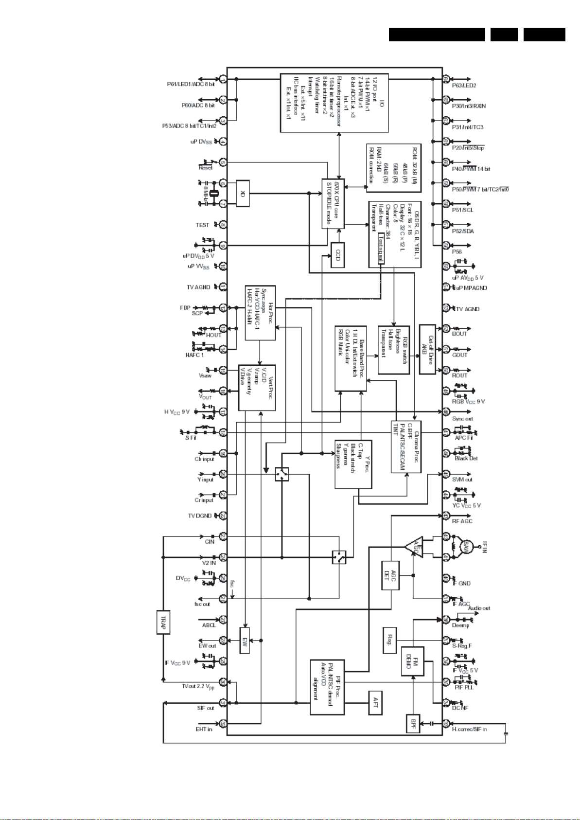
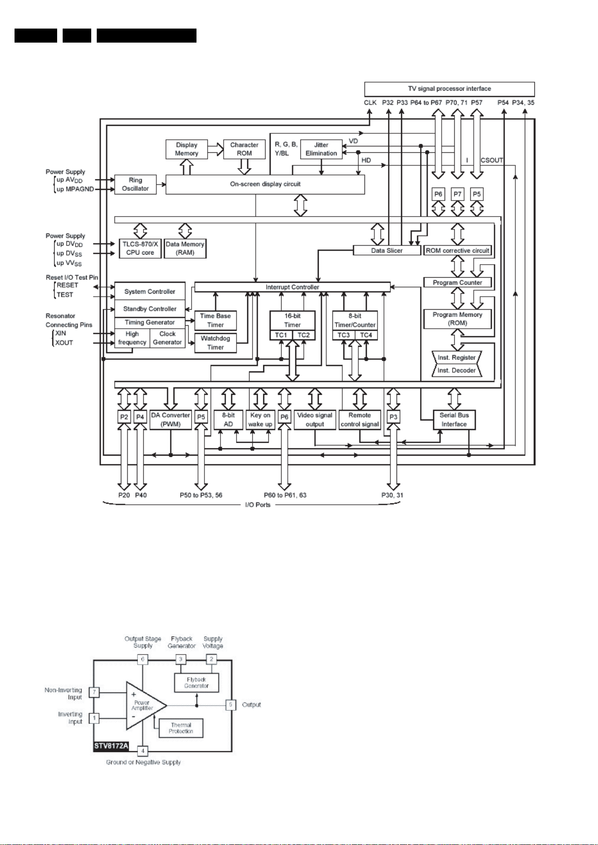
9.2.1 Main IC (IC101)
Description:
The main IC is a TMPA8857CSNG, provided by TOSHIBA. It is
an integrated circuit, suited for PAL, NTSC and SECAM TV. An
MCU and a TV signal processor are integrated in a 64 pin DIP
package.
The MCU contains an 8-bit CPU, ROM, RAM, I/O-ports, timer/
counters, A/D-converters, an on-screen display controller,
remote control interfaces, IIC bus interfaces, and the closed
caption decoder.
The TV signal processor contains PIF, SIF, Video, multistandard chroma, deflection, and RGB processors.
TV Processor
IF
• Integrated PIF VCO, aligned automatically
• Negative demodulation PIF
• Multi-frequency SIF demodulator, without external tankcoil
Video
• Integrated chroma traps
• Black stretch
• Y-gamma
Chroma
• Integrated chroma BPF’s
• PAL/NTSC/SECAM demodulation
RGB/Base-band
• Integrated 1 H base-band delay line
• Base-band TINT control
• Internal OSD interface
• Half-tone and transparent for OSD
• External YCbCr interface for DVD
• RGB cut-off/drive controls by bus
• ABCL (ABL and ACL combined)
Synchronization
• Integrated fH x 640 VCO
• DC coupled vertical ramp output (single)
• EW correction with EHT output
•Sync out
Features:
MCU:
• High speed 8-bit CPU
• 12 I/O ports
• I2C bus interface (multi-master)
• 14-bit PWM output, 1 channel, for a voltage synthesizer
• 7-bit PWM output, 1 channel
• 8-bit A/D converter, 3 channels
• Remote control signal preprocessor
• Two 16-bit internal timer/counters, 2 channels
• Two 8-bit internal timer/counters, 2 channels
• Time base timer
• Watchdog timer
• 16 interrupt sources: 5 external, 11 internal
• Stop and Idle power saving modes
CCD decoder
• Digital data slicer for NTSC
OSD
• Clock generation for OSD display
• Font ROM characters: 384 characters
• Characters display: 32 columns x 12 lines
• Composition: 16 x 18 dots
• Size of character: 3 (line by line)
• Color of character: 8 (character by character)
• Display position: H 256 / V 512 steps
• BOX function
• Fringing, smoothing, italic, underline function
• Conform to CCD regulation
• Jitter elimination
Page 21
Circuit Descriptions, Abbreviation List, and IC Data Sheets
EN 21TC5.1L CB 9.
Figure 9-6 Block Diagram Main IC 1
G_16340_026.eps
100306
Page 22
EN 22 TC5.1L CB9.
Circuit Descriptions, Abbreviation List, and IC Data Sheets
9.2.2 Vertical Deflection Booster (IC 301)
The STV8172A is a vertical deflection booster, designed for TV
and monitor applications.
This device, supplied with up to 35 V, provides a maximum
output current of 2.5 A, to drive the vertical deflection yoke.
The internal fly back generator delivers fallback voltages of up
to 75 V.
Figure 9-8 Vertical Deflection Booster
Figure 9-7 Block Diagram Main IC 2
G_16340_028.eps
100306
G_16340_027.eps
100306
Page 23
Circuit Descriptions, Abbreviation List, and IC Data Sheets
EN 23TC5.1L CB 9.
9.2.3 Demultiplexer (IC 901)
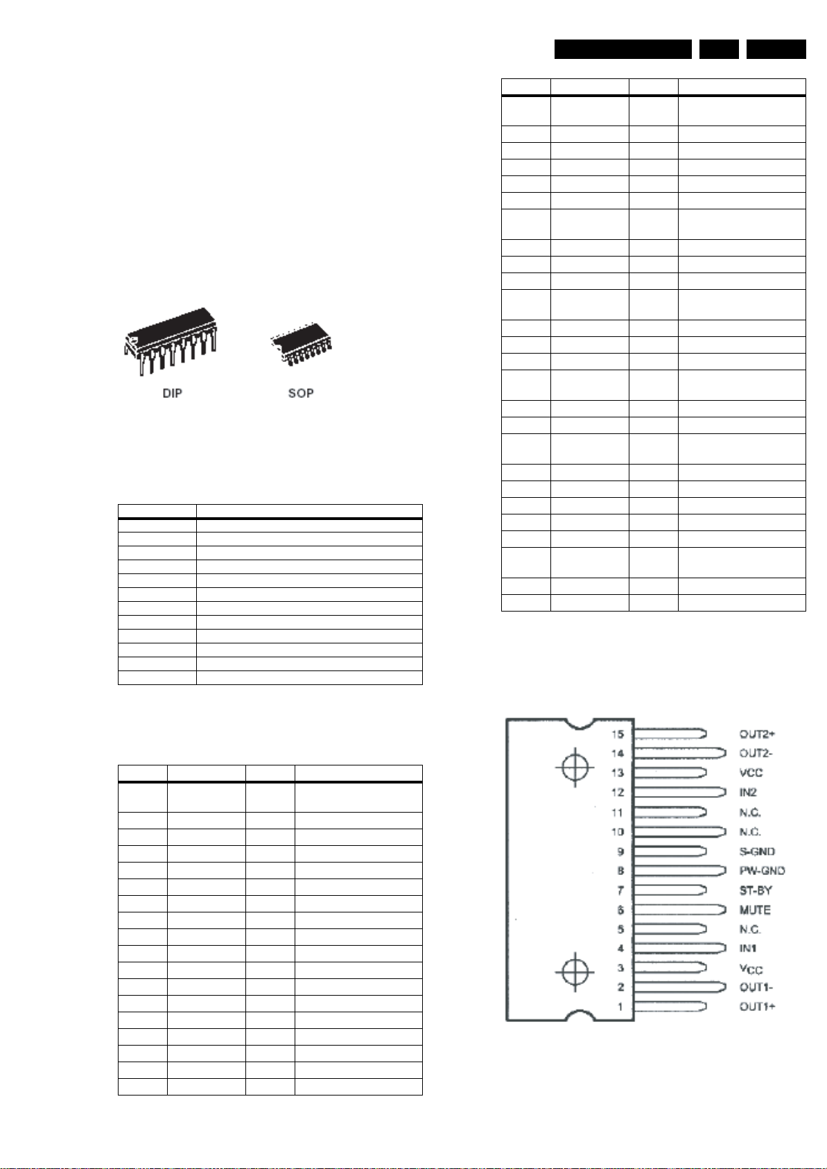
The HCF4052B is a monolithic integrated circuit, fabricated in
Metal Oxide Semiconductor technology, available in DIP and
SOP packages.
The HCF4052B analog multiplexer/demultiplexer is a digitally
controlled analog switch, having low ON impedance, and very
low OFF leakage current. This multiplexer circuit dissipates
extremely low quiescent power over the full supply voltage
range, independent of the logic states of the control signals.
When a logic “1” is present at the inhibit input, all channels are
off. This device is a differential 4-channel multiplexer, having 2
binary control inputs, A and B, and an inhibit input. The two
binary input signals select 1 of 4 pairs of channels to be turned
on and connect the analog inputs to the outputs.
G_16340_029.eps
100306
Figure 9-9 Demultiplexer
Table 9-3 Demultiplexer
PIN Symbol
1 and 2 Y CHANNELS IN/OUT
3 COMMON "Y" OUT/IN
4 and 5 Y CHANNELS IN/OUT
6INH
7 VEE
8 VSS
9B
10 A
11 and 12 X CHANNELS IN/OUT
13 COMMON "X" OUT/IN
14 and 15 X CHANNELS IN/OUT
16 VDD
9.2.4 Sound Processor (IC1001)
Pin No. Pin Name Type Short Description
19 DVSUP Digital power supply +5
V
20 DVSS Digital ground
21 I2S_DA_IN2 I2S2 data input
22 RESETQ IN Power-on-reset
23 NC Not connected
24 NC Not connected
25 VREF2 Reference ground 2
High-voltage part
26 DACM_R OUT Loudspeaker out, right
27 DACM_L OUT Loudspeaker out, left
28 NC Not connected
29 VREF1 Reference Ground 1
High voltage part
30 SC1_OUT_R OUT Audio 1 output, right
31 SC1_OUT_L OUT Audio 1 output, left
32 NC Not connected
33 AHVSUP Analog power supply
8.0V
34 CAPL_M Volume capacitor MAIN
35 AHVSS Analog ground
36 AGNDC Analog reference voltage
High-voltage part
37 SC2_IN_L IN Audio 2 input, left
38 SC2_IN_R IN Audio 2 input, right
39 ASG Analog shield Ground
40 SC1_IN_L IN Audio 1 input, left
41 SC1_IN_R IN Audio 1 input, right
42 VREFTOP Reference voltage IF A/D
converter
43 MONO_IN IN Mono input
44 AVSS Analog ground
9.2.5 Dual Bridge Amplifier (IC 602)
The TDA7266SA is a dual bridge amplifier, specially designed
for LCD monitor, PC motherboard, TV, and portable radio
applications.
Table 9-4 Sound Processor
Pin No. Pin Name Type Short Description
1 AVSUP Analog power supply
+5V
2 ANA_IN+ IN IF Input 1
3 ANA_IN- IN IF common
4 TESTEN IN Test pin
5 XTAL_IN IN Crystal oscillator
6 XTAL_OUT OUT Crystal oscillator
7 TP Test pin
8 D_CTR_I/O_1 IN/OUT D_CTR_I/O_1
9 D_CTR_I/O_0 IN/OUT D_CTR_I/O_0
10 ADR_SEL IN I2C BUS address select
11 STANDBYQ IN Stand-by ( Low-active)
12 I2C_CL IN/OUT I2C clock
13 I2C_DA IN/OUT I2C data
14 I2S_CL I2S clock
15 I2S_WS I2S word strobe
16 I2S_DA_OUT I2S data output
17 I2S_DA_IN1 I2S1 data input
18 ADR_CL ADR clock
G_16340_031.eps
100306
Figure 9-10 Dual Bridge Amplifier
Page 24
EN 24 TC5.1L CB10.
10. Spare Parts List
Spare Parts List
Set Level
Various
CRT 9965 100 08481 A68ERF185X013/MR
CRT 9965 100 08550 A68ERF185X013/ME
OTH021 9965 200 32564 CHASSIS MAINBOARD
OTH022 9965 200 32565 CRT assy
OTH051 9965 200 32330 Connector
OTH091 9965 200 32559 SP/LA assy
OTH093 9965 200 32557 Sound Process assy
OTH100 9965 200 32559 SP/LA assy
P911 9965 100 08478 TJC3-7Y/SCN-7Y
Main Board
Various
F801 9965 000 34538 GLASS TUBE FUSE
F801 9965 100 08475 FUSE T 3.15A 250V
FCONTR 9965 200 32574 IR & Control assy
FORD811 9965 000 14925 Bead BF60 for C508
P201 9965 000 34463 HS 5p TJC3-5Y
P202 9965 200 32330 Connector
P421 9965 000 34512 HS 4P24 550 TJC3-4Y
SOUND 9965 200 32557 BTSC Assy
TU101 9965 000 34483 FSNA05T-4-E
X001 9965 000 15136 Xtal 8.0MHz
X201 9965 000 15710 CER TRAP TPS 4.5MHZ
X202 9965 000 34511 CER.FILTER LT4.5MH
Z101 9965 000 22820 SAW FILTER F1859
g
C008 9965 000 34503 100pF 5% 50V
C01 9965 000 14036 100μF 20% 25V
C021 9965 000 27860 10μF /-20% 16V
C022 9965 100 07896 10nF 20% 50V
C025 9965 000 27860 10μF /-20% 16V
C026 9965 100 07896 10nF 20% 50V
C027 9965 100 07896 10nF 20% 50V
C028 9965 000 27860 10μF /-20% 16V
C029 9965 100 07896 10nF 20% 50V
C030 9965 000 31455 220pF 5% 50V
C031 9965 000 34506 39pF 5% 50V
C032 9965 000 34506 39pF 5% 50V
C033 9965 000 27860 10μF /-20% 16V
C034 9965 100 07896 10nF 20% 50V
C041 9965 000 27860 10μF /-20% 16V
C043 9965 100 07896 10nF 20% 50V
C101 9965 000 14039 4.7μF 20% 50V
C104 9965 000 15112 0.1μF 5% 50V
C105 9965 000 15686 100μF 20% 50V
C106 9965 100 07896 10nF 20% 50V
C107 9965 100 07896 10nF 20% 50V
C108 9965 100 07896 10nF 20% 50V
C109 9965 000 30711 1000pF 20% 50V
C209 9965 000 27860 10μF /-20% 16V
C210 9965 000 27871 33μF 20% 16V
C211 9965 000 15112 0.1μF 5% 50V
C212 9965 000 15057 4.7k 5% 0.16W
C213 9965 000 13961 47μF 20% 16V
C214 9965 100 07896 10nF 20% 50V
C216 9965 000 34500 0.22μF 10% 50V
C217 9965 000 30713 2.2nF 10% 50V
C218 9965 000 14037 1μF 20% 50V
C219 9965 000 14069 100μF 20% 16V
C220 9965 100 07896 10nF 20% 50V
C221 9965 000 14037 1μF 20% 50V
C223 9965 000 14039 4.7μF 20% 50V
C224 9965 000 14036 100μF 20% 25V
C225 9965 100 07896 10nF 20% 50V
C226 9965 000 30711 1000pF 20% 50V
C227 9965 000 15088 0.47μF 20% 50V
C228 9965 000 27860 10μF /-20% 16V
C229 9965 000 13961 47μF 20% 16V
C230 9965 000 15806 0.1μF +80-20% 50V
C231 9965 000 30713 2.2nF 10% 50V
C233 9965 000 14069 100μF 20% 16V
C234 9965 100 07896 10nF 20% 50V
C235 9965 000 27871 33μF 20% 16V
C236 9965 100 07896 10nF 20% 50V
C237 9965 000 14075 10μF 20% 50V
C238 9965 000 15112 0.1μF 5% 50V
C239 9965 100 07896 10nF 20% 50V
C241 9965 000 14037 1μF 20% 50V
C242 9965 000 15112 0.1μ
C243 9965 000 14037 1μF 20% 50V
C244 9965 100 07896 10nF 20% 50V
C245 9965 000 14599 470μF 20% 16V
C246 9965 000 34501 0.47μF 10%
C247 9965 000 17886 0.0082μF 5% 63V
C248 9965 000 34501 0.47μF 10%
C249 9965 000 14039 4.7μF 20% 50V
C250 9965 000 15182 47μF 20% 25V
C251 9965 000 14039 4.7μF 20% 50V
C254 9965 000 34507 47pF 5% 50V
C261 9965 100 07896 10nF 20% 50V
C262 9965 000 14070 220μF 20% 16V
C263 9965 000 14069 100μF 20% 16V
C264 9965 000 15112 0.1μF 5% 50V
C266 9965 000 15112 0.1μF 5% 50V
C280 9965 100 07896 10nF 20% 50V
C281 9965 100 07896 10nF 20% 50V
C301 9965 000 15684 220μF 20% 35V
C302 9965 000 14598 100μF 20% 35V
C303 9965 000 14075 10μF 20% 50V
C304 9965 000 15114 0.47μF 5% 50V
C305 9965 000 34509 0.68μF 5% 63V
C306 9965 000 34508 6800pF 10% 50V
C308 9965 000 15684 220μF 20% 35V
C309 9965 000 22941 0.33μF 63V 5% MPE
C311 9965 000 15697 2700pF 5% 100V
C315 9965 000 34502 68pF 5% 50V
C401 9965 000 22930 4.7μF 20% 160V
C402 9965 000 34505 3300pF 50V 10%
C403 9965 000 34461 390pF 5% 50V
C413 9965 100 08472 0.012μF 5% 400V
C415 9965 000 15682 Electrolytic Capacitor
C422 9965 000 34497 220μF 160V 20%
C431 9965 000 31455 220pF 5% 50V
C432 9965 000 34499 1000μF 20% 35V
C433 9965 000 15183 220pF 500V 10%
C435 9965 000 34499 1000μF 20% 35V
C441 9965 000 15183 220pF 500V 10%
C442 9965 000 34498 22μF 250V /-20%
C443 9965 000 14039 4.7μF 20% 50V
C451 9965 000 15700 0.056μF 5% 400V
C622 9965 000 15103 22pF 5% 50V
C623 9965 000 15103 22pF 5% 50V
C624 9965 000 14071 470μF 20% 25V
C625 9965 000 15112 0.1μF 5% 50V
C626 9965 000 34475 33
C627 9965 000 15113 220nF 5% 50V
C630 9965 000 34475 33μF 5% 63V
C631 9965 000 15113 220nF 5% 50V
C634 9965 000 34474 33μF 20% 50V
C661 9965 000 14036 100μF 20% 25V
C801 9965 000 35331 0.22μF 20% 250V
C802 9965 000 35331 0.22μF 20% 250V
C803 9965 000 24382 0.1μF 10% 400V
C804 9965 000 15188 4700pF 250Vac +80-20%
C804B 9965 000 17914 470pF 10% 400V
C805 9965 000 15188 4700pF 250Vac +80-20%
C805B 9965 000 17914 470pF 10% 400V
C806 9965 000 40946 220μF 20% 450V
C806 9965 100 07880 CAP.ELEC 200V 680UF
C807 9965 000 44381 10nF 10% 500V
C810 9965 000 31455 220pF 5% 50V
C811 9965 000 15719 3.3μF 20% 50V
C812 9965 000 30711 1000pF 20% 50V
C812 9965 000 34505 3300pF 50V 10%
C813 9965 000 15806 0.1μF +80-20% 50V
C814 9965 000 17906 10μF 20% 35V
C815 9965 000 38780 1000pF 10% 2KV
C815 9965 000 38974 1000pF 102KV
C816 9965 000 44728 10nF 20% 1kV
C817 9965 000 44729 220pF 10% 1kV
C820 9965 000 15183 220pF 500V 10%
C821 9965 000 22932 1000μF 20% 25V
C822 9965 100 07896 10nF 20% 50V
C826 9965 100 07882 470pF 10% 2KV
C827 9965 000 44381 10nF 10% 500V
C828 9965 100 07881 330μF 20%160V
C829 9965 000 14075 10μF 20% 50V
C831 9965 100 07896 10nF 20% 50V
C832 9965 000 17510 1000μF 16V 20%
C833 9965 000 34533 4700ΩF 16V 20%
C834 9965 100 07896 10nF 20% 50V
C835 9965 100 07896 10nF 20% 50V
C836 9965 000 14599 470μF 20% 16V
C840B 9965 100 03195 2200pF 20% 400VAC
C903 9965 000 13961 47μF 20% 16V
C904 9965 000 27860 10μF /-20% 16V
C905 9965 000 27860 10μF /-20% 16V
F 5% 50V
μF 5% 63V
C908 9965 000 13961 47μF 20% 16V
C909 9965 000 27860 10μF /-20% 16V
C910 9965 000 27860 10μF /-20% 16V
C911 9965 100 07896 10nF 20% 50V
C912 9965 000 14069 100μF 20% 16V
C913 9965 100 07896 10nF 20% 50V
C914 9965 000 14069 100μF 20% 16V
C924 9965 000 27860 10μF /-20% 16V
C925 9965 000 34504 33pF 50V /-5%
C926 9965 000 14070 220μF 20% 16V
C927 9965 000 27860 10μF /-20% 16V
C928 9965 000 27860 10μF /-20% 16V
C929 9965 100 07896 10nF 20% 50V
C930 9965 000 14069 100μF 20% 16V
f
R001 9965 000 14050 10k 5% 0.16W
R003 9965 100 02999 1kΩ 5% 1/6W
R004 9965 100 02999 1kΩ 5% 1/6W
R005 9965 000 15057 4.7k 5% 0.16W
R006 9965 000 15057 4.7k 5% 0.16W
R01 9965 000 15057 4.7k 5% 0.16W
R018 9965 000 14050 10k 5% 0.16W
R02 9965 000 27858 27kΩ 5% 1/6W
R023 9965 000 14049 100Ω 5% 0.16W
R024 9965 100 03127 47Ω 5% 1/6W
R025 9965 000 14050 10k 5% 0.16W
R026 9965 000 14050 10k 5% 0.16W
R030 9965 000 15773 4.7Ω 5% 0.25W
R031 9965 100 02999 1kΩ 5% 1/6W
R032 9965 100 02999 1kΩ 5% 1/6W
R033 9965 100 02999 1kΩ 5% 1/6W
R034 9965 000 14050 10k 5% 0.16W
R036 9965 000 13960 470Ω 5% 0.16W
R036A 9965 000 14050 10k 5% 0.16W
R043 9965 000 14050 10k 5% 0.16W
R044 9965 000 13957 2.2kΩ 5% 1/6W
R101 9965 000 14049 100Ω 5% 0.16W
R101A 9965 000 14049 100Ω 5% 0.16W
R102 9965 100 03110 150Ω 5% 1/6W
R103 9965 000 13960 470Ω 5% 0.16W
R104 9965 000 15047 22Ω 5% 1/6W
R106 9965 100 03000 680Ω 5% 1/6W
R107 9965 100 03140 56Ω 5% 1/6W
R108 9965 100 03110 150Ω 5% 1/6W
R209 9965 000 14050 10k 5% 0.16W
R211 9965 000 15057 4.7k 5% 0.16W
R212 9965 100 02996 1N4148 (Switching)
R213 9965 000 14050 10k 5% 0.16W
R214 9965 000 15050 270Ω 5% 0.16W
R215 9965 000 15050 270Ω 5% 0.16W
R216 9965 000 15050 270Ω 5% 0.16W
R219 9965 100 03123 30kΩ 5% 1/6W
R220 9965 100 03120 220kΩ 5% 1/6W
R222 9965 000 15041 100k 5% 0.16W
R223 9965 000 15041 100k 5% 0.16W
R225 9965 000 13959 330Ω 5% 1/6W
R226 9965 000 14049 100Ω 5% 0.16W
R227 9965 000 15050 270Ω 5% 0.16W
R228 9965 000 14050 10k 5% 0.16W
R229 9965 000 15049 24kΩ 5% 1/6W
R230 9965 000 15049 24kΩ 5% 1/6W
R231 9965 000 14055 33kΩ
R232 9965 000 14049 100Ω 5% 0.16W
R233 9965 000 13959 330Ω 5% 1/6W
R233A 9965 000 31774 3.3kΩ 5% 0.16W
R234 9965 000 14049 100Ω 5% 0.16W
R235 9965 000 17494 120Ω 5% 1/6W
R238 9965 000 13960 470Ω 5% 0.16W
R239 9965 100 02999 1kΩ 5% 1/6W
R241 9965 000 15050 270Ω 5% 0.16W
R242 9965 000 14049 100Ω 5% 0.16W
R243 9965 000 14049 100Ω 5% 0.16W
R244 9965 100 03090 BAT85 (Switch.)
R245 9965 000 14049 100Ω 5% 0.16W
R246 9965 100 03146 8.2kΩ 5% 1/6W
R247 9965 000 13959 330Ω 5% 1/6W
R248 9965 100 02999 1kΩ 5% 1/6W
R250 9965 100 07901 180Ω 5% 1/6W
R251 9965 000 13960 470Ω 5% 0.16W
R253 9965 000 15041 100k 5% 0.16W
R254 9965 000 15041 100k 5% 0.16W
R255 9965 000 31773 150W 5% 0.16W
R256 9965 100 06101 5.6kΩ 5% 1/6W
R257 9965 000 15057 4.7k 5% 0.16W
R258 9965 100 03110 150Ω 5% 1/6W
R261 9965 000 13959 330Ω 5% 1/6W
R262 9965 100 03107 1.2kΩ 5% 1/6W
5% 1/6W
Page 25
Spare Parts List
EN 25TC5.1L CB 10.
R266 9965 000 15777 22kΩ 1% 2W
R302 9965 000 34492 3.9kΩ 1% 1/4W
R303 9965 000 34491 33kΩ 1% 1/4W
R304 9965 000 34494 0.68Ω 1W
R309 9965 100 07903 180Ω 5% 1W
R310 9965 000 14050 10kΩ 5% 0.16W
R311 9965 000 34489 10kΩ 1% 1/4W
R312 9965 000 34490 18kΩ 1% 1/4W
R313 9965 000 34495 1.5Ω 2W
R316 9965 000 34488 10kΩ 5% 1/2W
R401 9965 100 03114 220Ω 5% 1/6W
R402 9965 000 15676 2.4kΩ 5% 1W
R404 9965 000 34517 4.7kΩ 5% 7W
R412 9965 000 14054 2kΩ 5% 1/6W
R413 9965 000 14053 15kΩ 5% 1/6W
R414 9965 000 14585 47kΩ 5% 1/6W
R415 9965 000 15678 3.9Ω 5% 2W
R417 9965 000 13957 2.2kΩ 5% 1/6W
R418 9965 000 15057 4.7kΩ 5% 0.16W
R419 9965 100 07904 680Ω 5% 2W
R420 9965 000 13957 2.2kΩ 5% 1/6W
R420A 9965 000 13957 2.2kΩ 5% 1/6W
R422 9965 100 07878 0.47Ω 5% 2W
R423 9965 100 07878 0.47Ω 5% 2W
R424 9965 000 14050 10kΩ 5% 0.16W
R431 9965 100 07902 0.68Ω 5% 2W
R433 9965 100 07902 0.68Ω 5% 2W
R442 9965 100 07877 1Ω 5% 1/2W
R453 9965 100 02999 1kΩ 5% 1/6W
R460 9965 000 22907 150kΩ 5% 1/2W
R605 9965 000 14585 47kΩ 5% 1/6W
R605A 9965 000 17864 820Ω 5% 0.16W
R606 9965 000 14050 10kΩ 5% 0.16W
R608 9965 100 02999 1kΩ
R610 9965 000 14585 47kΩ 5% 1/6W
R611 9965 000 22999 0.47Ω 2W
R612 9965 100 02999 1kΩ 5% 1/6W
R618 9965 000 14050 10k 5% 0.16W
R656 9965 000 14050 10k 5% 0.16W
R801 9965 000 17901 1M 5% 0.5W
R810 9965 000 30822 68kΩ 5% 2W
R810 9965 100 08473 100kΩ 5% 2W
R811 9965 100 02999 1kΩ 5% 1/6W
R812 9965 100 02999 1kΩ 5% 1/6W
R813 9965 000 34528 15Ω 5% 1/2W
R814 9965 000 34526 1.5kΩ 5% 1/4W
R815 9965 000 14049 100Ω 5% 0.16W
R816 9965 000 34531 0.12Ω 2W Wire Wound
R816 9965 100 08474 0.15Ω 5% 2W
R817 9965 100 08476 100kΩ
R820 9965 000 34539 FUSE 5A 250VAC
R821 9965 000 34537 FUSE 3A 250VAC
R823A 9965 000 34537 FUSE 3A 250VAC
R825 9965 000 15664 2.2kΩ 5% 1/4W
R826 9965 000 34529 10Ω 5% 2W
R827 9965 000 34530 4.7kΩ 5% 5W
R828 9965 000 15777 22kΩ 5% 2W
R829 9965 000 14050 10k 5% 0.16W
R830 9965 100 02999 1kΩ 5% 1/6W
R831 9965 000 14055 33kΩ 5% 1/6W
R832 9965 000 14050 10kΩ 5% 0.16W
R833 9965 000 14050 10kΩ 5% 0.16W
R834 9965 000 34525 820kΩ 5%1/6W
R834A 9965 000 34527 6.8kΩ 1% 1/4W
R834B 9965 000 22797 390kΩ 1%1/4W
R835 9965 000 26502 0.12MΩ 1% 1/2W
R836 9965 000 15771 1KΩ 1/4W 5% Carb. Film
R837 9965 000 14050 10k 5% 0.16W
R838 9965 000 14050 10k 5% 0.16W
R840B 9965 000 17902 8.2M 5% 1W
R901 9965 100 03144 82Ω 5% 1/6W
R902 9965 100 03144 82Ω 5% 1/6W
R903 9965 000 31773 150W 5% 0.16W
R904 9965 100 02999 1kΩ 5% 1/6W
R905 9965 000 31773 150W 5% 0.16W
R906 9965 100 02999 1kΩ 5% 1/6W
R908 9965 100 03144 82Ω
R910 9965 100 02999 1kΩ 5% 1/6W
R911 9965 100 02999 1kΩ 5% 1/6W
R912 9965 100 02999 1kΩ 5% 1/6W
R913 9965 100 02999 1kΩ 5% 1/6W
R914 9965 100 03144 82Ω 5% 1/6W
R915 9965 100 03144 82Ω 5% 1/6W
R916 9965 100 02999 1kΩ 5% 1/6W
R917 9965 100 02999 1kΩ 5% 1/6W
R920 9965 000 14049 100Ω 5% 0.16W
R923 9965 100 03143 75Ω 5% 1/6W
R924 9965 100 02999 1kΩ 5% 1/6W
R925 9965 100 02999 1kΩ 5% 1/6W
R930 9965 100 03114 220Ω 5% 1/6W
R931 9965 100 03114 220Ω 5% 1/6W
R932 9965 100 02999 1kΩ 5% 1/6W
R932A 9965 100 02999 1kΩ 5% 1/6W
R933 9965 000 14053 15kΩ 5% 1/6W
5% 1/6W
5% 1/6W
R934 9965 100 02999 1kΩ 5% 1/6W
R934A 9965 100 02999 1kΩ 5% 1/6W
R935 9965 000 31773 150W 5% 0.16W
R936 9965 100 02999 1kΩ 5% 1/6W
R937 9965 000 14048 10Ω 5% 1/6W
R944 9965 000 14050 10k 5% 0.16W
R945 9965 000 14050 10k 5% 0.16W
R946 9965 100 03107 1.2kΩ 5% 1/6W
R946A 9965 000 13957 2.2kΩ 5% 1/6W
R947 9965 000 15041 100k 5% 0.16W
R948 9965 100 02999 1kΩ 5% 1/6W
R951 9965 000 31773 150W 5% 0.16W
R952 9965 000 31773 150W 5% 0.16W
R953 9965 000 31773 150W 5% 0.16W
R954 9965 000 31773 150W 5% 0.16W
RL01 9965 000 23783 Relay SS-112DM 12V
RT801 9965 000 27862 POSISTOR MZ75-9RM
RT802 9965 000 44720 NTC 2.5D-18LCS
VR802 9965 000 34532 TRIMMER B330 HORIZ
TYPE
b
L001 9965 100 07874 Bead
L002 9965 000 15123 10μH 5%
L101 9965 000 24356 COIL PL - 47 UH +/-5%
L102 9965 000 15121 1μH 10%
L204 9965 000 15124 22μH 5%
L205 9965 000 15124 22μH 5%
L206 9965 000 15124 22μH 5%
L208 9965 000 15124 22μH 5%
L209 9965 000 15123 10μH 5%
L212 9965 000 15123 10μH 5%
L301 9965 000 22943 Bead
L413 9965 100 07876 COIL WIDTH 1 MH
L801 9965 000 15193 100μH 10%
L802 9965 100 07874 Bead
L803 9965 100 03165 Bead BF-I35050R-730
L804 9965 100 03165 Bead BF-I35050R-730
T401 9965 000 17887 Transf. Hor. Drive
T801 9965 000 34535 10μH LCL-2802B
T801 9965 000 44735 LGH2V-40μH
T802 9965 000 22946 Line Filter 20μH
T802 9965 000 34535 10μH LCL-2802B
T803 9965 000 34536 BCK-4201-78
T803 9965 100 08477 BCK-42-0300
d
D001 9965 000 15651 5V-5V2 1/2W
D01 9965 100 02996 1N4148 (Switching)
D02 9965 100 02996 1N4148 (Switching)
D101 9965 100 03098 DIODE CW574CD
D202 9965 100 02996 1N4148 (Switching)
D203 9965 100 02996 1N4148 (Switching)
D204 9965 100 02996 1N4148 (Switching)
D205 9965 100 02996 1N4148 (Switching)
D206 9965 100 02996 1N4148 (Switching)
D207 9965 000 15818 BZX79-C6V2
D208 9965 100 02996 1N4148 (Switching)
D209 9965 000 14045 2V4 1/2W 5%
D210 9965 100 07898 24V 1/2W 5%
D211 9965 100 02996 1N4148 (Switching)
D212 9965 100 02996 1N4148 (Switching)
D213 9965 000 15817 3V9 1/2W 5%
D214 9965 100 02996 1N4148 (Switching)
D215 9965 100 02996 1N4148 (Switching)
D262 9965 100 02996 1N4148 (Switching)
D301 9965 100 03094 1N4001 (Rectifier)
D303 9965 100 05977 8V2 1/2W 5%
D304 9965 100 03091 FR104 (Fast Rectifier)
D309 9965 000 34484 BZV85-C51 1.3W-51V
D310 9965 100 02996 1N4148 (Switching)
D410 9965 100 02996 1N4148 (Switching)
D411 9965 100 06104 BY228
D412 9965 100 03091 FR104 (Fast Rectifier)
D420 9965 100 03091 FR104 (Fast Rectifier)
D431 9965 100 03091 FR104 (Fast Rectifier)
D432 9965 100 03091 FR104 (Fast Rectifier)
D441 9965 100 03091 FR104 (Fast Rectifier)
D602 9965 000 31774 3.3kΩ 5% 0.16W
D810 9965 100 03091 FR104 (Fast Rectifier)
D811 9965 100 03091 FR104 (Fast Rectifier)
D812 9965 100 02996 1N4148 (Switching)
D813 9965 000 15818 BZX79-C6V2
D816 9965 000 20421 1H8
D820 9965 000 22883 RU4YX
D822 9965 000 34522 RU4AMS
D823 9965 000 25702 SR3100
D824 9965 100 03094 1N4001 (Rectifier)
D826 9965 100 05977 8V2 1/2W 5%
D827 9965 100 02996 1N4148 (Switching)
D828 9965 100 06119 BZX79B6V2 +/-2%
D829 9965 100 02996 1N4148 (Switching)
D834 9965 100 06107 9V1 1/2W 5%
DB801 9965 000 22884 D3SB60 Bridge Rect.
ce
IC001 9965 000 17857 M24C08
IC101 9965 000 38193 TMPA8857PSNG
IC201 9965 000 34485 IC L7809 SGS (TO-220)
IC202 9965 100 03102 +5V 1.5A IC L7805CV
IC301 9965 000 30670 IC STV8172
IC602 9965 000 34473 IC TDA7266SA
IC801 9965 000 34524 STR-W6735
IC801 9965 100 08690 IC STR-W6756
IC802 9965 000 27867 PS2561L1-1-V
IC901 9965 000 15655 IC 4052
Q007 9965 100 03003 2SC1815-Y
Q008 9965 100 02997 ST2SA1015Y (PNP)
Q01 9965 000 34540 2SC2236-Y
Q101 9965 000 14974 2SC3779D
Q202 9965 100 03003 2SC1815-Y
Q203 9965 100 03003 2SC1815-Y
Q204 9965 100 03003 2SC1815-Y
Q205 9965 100 02997 ST2SA1015Y (PNP)
Q208 9965 100 07899 2SA817A-Y
Q209 9965 100 05966 PDTC124ES (NPN)
Q401 9965 100 02998 2SC2482
Q402 9965 100 03003 2SC1815-Y
Q411 9965 000 32929 NPN BU2520DX
Q412 9965 100 02997 ST2SA1015Y (PNP)
Q413 9965 100 02997 ST2SA1015Y (PNP)
Q414 9965 100 08471 IRFS630B
Q415 9965 100 03003 2SC1815-Y
Q601 9965 100 03003 2SC1815-Y
Q602 9965 100 02997 ST2SA1015Y (PNP)
Q603 9965 100 05966 PDTC124ES (NPN)
Q820 9965 000 34523 2SC2230Y
Q821 9965 000 15587 2SC4544
Q822 9965 100 03003 2SC1815-Y
Q823 9965 100 03003 2SC1815-Y
Q824 9965 100 03003 2SC1815-Y
Q825 9965 100 03003 2SC1815-Y
Q901 9965 100 03003 2SC1815-Y
Q902 9965 100 03003 2SC1815-Y
Q903 9965 100 03003 2SC1815-Y
Q904 9965 100 03003 2SC1815-Y
Q911 9965 100 03003 2SC1815-Y
Q912 9965 100 02997 ST2SA1015Y (PNP)
Q917 9965 100 03003 2SC1815-Y
Q918 9965 100 05966 PDTC124ES (NPN)
Q919 9965 100 05966 PDTC124ES (NPN)
J215 9965 000 14050 10k 5% 0.16W
J310 9965 100 02996 1N4148 (Switching)
J603 9965 000 34510 2.2μH 10%
J604 9965 000 34510 2.2μH 10%
J806 9965 100 07874 Bead
CRT Panel
Various
S501 9965 000 34422 CRT Sock. GZS10-2-108
g
C411 9965 000 34427 0.0039μF 5% 1.6kV
C412 9965 100 08483 0.0063μF 5% 1.6kV
C414 9965 100 08483 0.0063μF 5% 1.6kV
C419 9965 100 07895 0.33μF 5% 400V
C501 9965 000 34461 390pF 5% 50V
C502 9965 000 31199 470pF 5% 50V
C503 9965 000 31199 470pF 5% 50V
C504 9965 000 14921 10μF 20% 250V
C505 9965 000 44382 1000pF 10% 2kV
C506 9965 000 14599 470μF 20% 16V
C508 9965 000 14925 Bead BF60 for C508
C508 9965 100 07896 10nF 20% 50V
C509 9965 100 07896 10nF 20% 50V
f
R416 9965 000 15057 4.7k 5% 0.16W
R432 9965 100 03146 8.2kΩ 5% 1/6W
R461 9965 100 08482 10kΩ 5% 1/2W
R461 9965 100 08549 10kΩ 5% 1/2W
R461A 9965 100 08482 10kΩ 5% 1/2W
R461A 9965 100 08549 10kΩ 5% 1/2W
R501 9965 100 05971 560 Ohm 5% 1/6W
R502 9965 100 03000 680Ω 5% 1/6W
Page 26
EN 26 TC5.1L CB10.
Spare Parts List
R503 9965 100 03000 680Ω 5% 1/6W
R505 9965 100 05971 560Ω 5% 1/6W
R506 9965 100 03000 680Ω 5% 1/6W
R508 9965 100 03000 680Ω 5% 1/6W
R509 9965 100 03000 680Ω 5% 1/6W
R510 9965 100 05971 560Ω 5% 1/6W
R511 9965 100 03000 680Ω 5% 1/6W
R513 9965 100 03000 680Ω 5% 1/6W
R514 9965 100 03121 2.7kΩ 5% 1/6W
R515 9965 100 02999 1kΩ 5% 1/6W
R516 9965 000 15589 18kΩ 5% 1/2W
R517 9965 000 15589 18kΩ 5% 1/2W
R518 9965 000 15589 18kΩ 5% 1/2W
R519 9965 100 03001 2.7kΩ 5% 1/2W
R520 9965 100 03001 2.7kΩ 5% 1/2W
R521 9965 100 03001 2.7kΩ 5% 1/2W
R522 9965 100 03000 680Ω 5% 1/6W
b
L414 9965 100 08484 18μH
L501 9965 100 02996 1N4148 (Switching)
L503 9965 000 15411 10μH 10%
T402 9965 000 34428 FBT BSC27-0101Q
d
D501 9965 100 02996 1N4148 (Switching)
D502 9965 100 02996 1N4148 (Switching)
ce
Q501 9965 000 15587 2SC4544
Q502 9965 100 03003 2SC1815-Y
Q503 9965 000 15587 2SC4544
Q504 9965 100 03003 2SC1815-Y
Q505 9965 000 15587 2SC4544
Q506 9965 100 03003 2SC1815-Y
Q507 9965 000 14915 2SA562TM-0
OTH106 9965 000 34424 HS 4p 500/13 TJC1-4Y
OTH117 9965 000 34424 HS 4p 500/13 TJC1-4Y
IR & Front Control Panel
Various
IR001A 9965 000 27288 IR Receiver Module
P001B 9965 100 07897 HS 5P 2468#24 400MM
P002A 9965 000 27970 PIN BASE VH-3AW
P002B 9965 000 33614 3PIN BASE
S001A 9965 000 17540 Switch
S002A 9965 000 17540 Switch
S003A 9965 000 17540 Switch
S004A 9965 000 17540 Switch
SW001 9965 100 08469 POWER SOCKET PS6
g
C070A 9965 000 13961 47μF 20% 16V
CORD 9965 100 08468 206 P0WER CORD
C1006 9965 000 15112 0.1μF 5% 50V
C1008 9965 000 15112 0.1μF 5% 50V
C1009 9965 000 27860 10μF /-20% 16V
C1010 9965 000 15719 3.3μF 20% 50V
C1011 9965 000 15112 0.1μF 5% 50V
C1012 9965 000 20357 1000PF 50V 5% 0603
C1013 9965 000 27860 10μF /-20% 16V
C1014 9965 000 27860 10μF /-20% 16V
C1015 9965 000 27860 10μF /-20% 16V
C1016 9965 000 27860 10μF /-20% 16V
C1018 9965 000 20357 1000PF 50V 5% 0603
C1019 9965 000 20357 1000PF 50V 5% 0603
C1025 9965 000 14012 470pF 5% 50V 0603
C1031 9965 000 20344 10nF 50V +80-20% 0603
C1033 9965 000 20344 10nF 50V +80-20% 0603
C1034 9965 000 20344 10nF 50V +80-20% 0603
C1035 9965 000 14011 22pF 5% 50V
C1036 9965 000 14011 22pF 5% 50V
C1037 9965 000 15112 0.1μF 5% 50V
C1038 9965 000 13961 47μF 20% 16V
C1039 9965 000 15114 0.47μF 5% 50V
C1040 9965 000 20357 1000pF 50V 5% 0603
C1041 9965 000 20357 1000pF 50V 5% 0603
C1042 9965 000 15084 22μF 20% 16V
C1043 9965 000 14008 0.1uF 50V +80%~-20%
C1044 9965 000 20349 220pF 5% 50V 0603
C1045 9965 000 20349 220pF 5% 50V 0603
f
J1001 9965 000 27224 0Ω 5% 1/10W 0603
J1002 9965 000 27224 0Ω 5% 1/10W 0603
J1003 9965 000 27224 0Ω 5% 1/10W 0603
J1010 9965 000 27224 0Ω 5% 1/10W 0603
J1011 9965 000 27224 0Ω 5% 1/10W 0603
J1012 9965 000 27224 0Ω 5% 1/10W 0603
J1013 9965 000 27224 0Ω 5% 1/10W 0603
J1014 9965 000 27224 0Ω 5% 1/10W 0603
R1001 9965 000 13987 100Ω 5% 1/16W
R1002 9965 000 13987 100Ω 5% 1/16W
R1003 9965 000 13990 100kΩ 5% /16W
R1005 9965 000 13996 3.3kΩ 5% /16W
R1006 9965 100 08479 47Ω 5% 1/16W
R1007 9965 100 08486 1.5kΩ 5% /16W 1206
R1008 9965 000 13990 100kΩ 5% /16W
R1014 9965 000 13988 1kΩ 5% /16W
R1015 9965 000 13988 1kΩ 5% /16W
R1016 9965 000 13988 1kΩ 5% /16W
R1017 9965 000 13988 1kΩ 5% /16W
b
L1001 9965 000 15124 22μH 5%
L1002 9965 000 15124 22μH 5%
ce
IC1001 9965 000 25711 IC MSP3425G
Q1003 9965 100 03003 2SC1815-Y
Q1005 9965 100 08485 BC847A (NPN)
Q1006 9965 100 08485 BC847A (NPN)
f
R025A 9965 000 24332 2.4Ω 5% 1/6W
R027A 9965 000 17896 3.6kΩ 5% 1/6W
R028A 9965 000 27858 27kΩ 5% 1/6W
R029A 9965 100 03146 8.2kΩ 5% 1/6W
R033B 9965 000 13960 470Ω 5% 0.16W
R070A 9965 100 03127 47Ω 5% 1/6W
d
D1001A 9965 000 32018 LED 932205099682
OTH023 9965 100 08467 HS 2P 1617#22 300
BTSC Panel
Various
X1001 9965 000 26861 18.432MHZ(CL=12PF)
g
C1001 9965 000 30782 3.3pF 50V
C1002 9965 000 30782 3.3pF 50V
C1004 9965 000 27330 56pF 5% 50V 0603
C1005 9965 000 27330 56pF 5% 50V 0603
Page 27

11. Revision List
Manual xxxx xxx xxxx.0
• First release.
Revision List
EN 27TC5.1L CB 11.
 Loading...