

Page 1

User Manual
VX4469A
ARINC 629 Communication Module
070-9147-01
This document supports firmware version 1.00
and above.
Page 2

Copyright E T ektronix, Inc. All rights reserved.
T ektronix products are covered by U.S. and foreign patents, issued and pending. Information in this publication supercedes
that in all previously published material. Specifications and price change privileges reserved.
Printed in the U.S.A.
T ektronix, Inc., P.O. Box 1000, Wilsonville, OR 97070–1000
TEKTRONIX and TEK are registered trademarks of T ektronix, Inc.
Page 3

WARRANTY
T ektronix warrants that this product will be free from defects in materials and workmanship for a period of three (3) years
from the date of shipment. If any such product proves defective during this warranty period, T ektronix, at its option, either
will repair the defective product without charge for parts and labor, or will provide a replacement in exchange for the
defective product.
In order to obtain service under this warranty, Customer must notify Tektronix of the defect before the expiration of the
warranty period and make suitable arrangements for the performance of service. Customer shall be responsible for
packaging and shipping the defective product to the service center designated by T ektronix, with shipping charges prepaid.
T ektronix shall pay for the return of the product to Customer if the shipment is to a location within the country in which the
T ektronix service center is located. Customer shall be responsible for paying all shipping charges, duties, taxes, and any
other charges for products returned to any other locations.
This warranty shall not apply to any defect, failure or damage caused by improper use or improper or inadequate
maintenance and care. T ektronix shall not be obligated to furnish service under this warranty a) to repair damage resulting
from attempts by personnel other than T ektronix representatives to install, repair or service the product; b) to repair
damage resulting from improper use or connection to incompatible equipment; or c) to service a product that has been
modified or integrated with other products when the effect of such modification or integration increases the time or
difficulty of servicing the product.
THIS WARRANTY IS GIVEN BY TEKTRONIX WITH RESPECT TO THIS PRODUCT IN LIEU OF ANY
OTHER WARRANTIES, EXPRESSED OR IMPLIED. TEKTRONIX AND ITS VENDORS DISCLAIM ANY
IMPLIED WARRANTIES OF MERCHANTABILITY OR FITNESS FOR A PARTICULAR PURPOSE.
TEKTRONIX’ RESPONSIBILITY TO REPAIR OR REPLACE DEFECTIVE PRODUCTS IS THE SOLE AND
EXCLUSIVE REMEDY PROVIDED TO THE CUST OMER FOR BREACH OF THIS WARRANTY. TEKTRONIX
AND ITS VENDORS WILL NOT BE LIABLE FOR ANY INDIRECT , SPECIAL, INCIDENTAL, OR
CONSEQUENTIAL DAMAGES IRRESPECTIVE OF WHETHER TEKTRONIX OR THE VENDOR HAS
ADVANCE NOTICE OF THE POSSIBILITY OF SUCH DAMAGES.
Page 4

Page 5

EC Declaration of Conformity
We
Tektronix Holland N.V.
Marktweg 73A
8444 AB Heerenveen
The Netherlands
declare under sole responsibility that the
VX4469A and all options
meets the intent of Directive 89/336/EEC for Electromagnetic Compatibility.
Compliance was demonstrated to the following specifications as listed in the Official
Journal of the European Communities:
EN 55011 Class A Radiated and Conducted Emissions
EN 50081-1 Emissions:
EN 55022 Class B Radiated and Conducted Emissions
EN 50082-1 Immunity:
IEC 801-2 Electrostatic Discharge Immunity
IEC 801-3 RF Electromagnetic Field Immunity
IEC 801-4 Electrical Fast Transient/Burst Immunity
IEC 801-5 Power Line Surge Immunity
To ensure compliance with EMC requirements this module must be installed in a
mainframe which has backplane shields installed which comply with Rule B.7.45 of
the VXIbus Specification. Only high quality shielded cables having a reliable,
continuous outer shield (braid & foil) which has low impedance connections to
shielded connector housings at both ends should be connected to this product. In
addition, each twisted pair in the cable connected to the S2 port should be individually
shielded.
Page 6

Page 7

Table of Contents
Getting Started
Operating Basics
General Safety Summary vii. . . . . . . . . . . . . . . . . . . . . . . . . . . . . . . . . . . .
Service Safety Summary xi. . . . . . . . . . . . . . . . . . . . . . . . . . . . . . . . . . . . .
Preface xiii. . . . . . . . . . . . . . . . . . . . . . . . . . . . . . . . . . . . . . . . . . . . . . . . . . .
Product Description 1–1. . . . . . . . . . . . . . . . . . . . . . . . . . . . . . . . . . . . . . . . . . . . . . .
Accessories 1–4. . . . . . . . . . . . . . . . . . . . . . . . . . . . . . . . . . . . . . . . . . . . . . . . . . . . . .
Controls And Indicators 1–6. . . . . . . . . . . . . . . . . . . . . . . . . . . . . . . . . . . . . . . . . . . .
Configuration 1–8. . . . . . . . . . . . . . . . . . . . . . . . . . . . . . . . . . . . . . . . . . . . . . . . . . . .
Installation 1–11. . . . . . . . . . . . . . . . . . . . . . . . . . . . . . . . . . . . . . . . . . . . . . . . . . . . . .
Installation Checklist 1–13. . . . . . . . . . . . . . . . . . . . . . . . . . . . . . . . . . . . . . . . . . . . . .
Functional Check 2–1. . . . . . . . . . . . . . . . . . . . . . . . . . . . . . . . . . . . . . . . . . . . . . . . .
Functional Overview 2–2. . . . . . . . . . . . . . . . . . . . . . . . . . . . . . . . . . . . . . . . . . . . . .
Power-on 2–3. . . . . . . . . . . . . . . . . . . . . . . . . . . . . . . . . . . . . . . . . . . . . . . . . . . . . . .
VXIbus Basics 2–3. . . . . . . . . . . . . . . . . . . . . . . . . . . . . . . . . . . . . . . . . . . . . . . . . . .
ARINC 629 2–6. . . . . . . . . . . . . . . . . . . . . . . . . . . . . . . . . . . . . . . . . . . . . . . .
Protocol Timers 2–6. . . . . . . . . . . . . . . . . . . . . . . . . . . . . . . . . . . . . . . . . . . . . . . . . .
Modes 2–7. . . . . . . . . . . . . . . . . . . . . . . . . . . . . . . . . . . . . . . . . . . . . . . . . . . . . . . . . .
Instrument I/O 2–7. . . . . . . . . . . . . . . . . . . . . . . . . . . . . . . . . . . . . . . . . . . . . . . . . . .
Syntax and Commands
Status and Events
Command Syntax 3–1. . . . . . . . . . . . . . . . . . . . . . . . . . . . . . . . . . . . . . . . . .
Functional Command Groups 3–3. . . . . . . . . . . . . . . . . . . . . . . . . . . . . . . .
System Commands 3–3. . . . . . . . . . . . . . . . . . . . . . . . . . . . . . . . . . . . . . . . . . . . . . . .
Module Commands 3–4. . . . . . . . . . . . . . . . . . . . . . . . . . . . . . . . . . . . . . . . . . . . . . .
Command Summary 3–4. . . . . . . . . . . . . . . . . . . . . . . . . . . . . . . . . . . . . . . . . . . . . . .
Command Descriptions 3–11. . . . . . . . . . . . . . . . . . . . . . . . . . . . . . . . . . . . . .
Programming Examples 3–139. . . . . . . . . . . . . . . . . . . . . . . . . . . . . . . . . . . . .
Status 4–1. . . . . . . . . . . . . . . . . . . . . . . . . . . . . . . . . . . . . . . . . . . . . . . . . . . . . . . . . .
Power LED 4–1. . . . . . . . . . . . . . . . . . . . . . . . . . . . . . . . . . . . . . . . . . . . . . . . . .
Failed LED 4–1. . . . . . . . . . . . . . . . . . . . . . . . . . . . . . . . . . . . . . . . . . . . . . . . . .
MSG LED 4–1. . . . . . . . . . . . . . . . . . . . . . . . . . . . . . . . . . . . . . . . . . . . . . . . . . .
ERROR 4–1. . . . . . . . . . . . . . . . . . . . . . . . . . . . . . . . . . . . . . . . . . . . . . . . . . . . .
BACKGROUND 4–1. . . . . . . . . . . . . . . . . . . . . . . . . . . . . . . . . . . . . . . . . . . . .
LED 4–1. . . . . . . . . . . . . . . . . . . . . . . . . . . . . . . . . . . . . . . . . . . . . . . . . . . . . . . .
Events 4–2. . . . . . . . . . . . . . . . . . . . . . . . . . . . . . . . . . . . . . . . . . . . . . . . . . . . . . . . . .
VX4469A ARINC 629 Communication Module User Manual
i
Page 8

Table of Contents
Appendices
Appendix A: Specifications A–1. . . . . . . . . . . . . . . . . . . . . . . . . . . . . . . . . . .
Appendix B: Input/Output Connections B–1. . . . . . . . . . . . . . . . . . . . . . . .
Appendix C: Trigger Lines C–1. . . . . . . . . . . . . . . . . . . . . . . . . . . . . . . . . . .
Appendix D: Performance Verification D–1. . . . . . . . . . . . . . . . . . . . . . . . .
Appendix E: Front Panel Data Port E–1. . . . . . . . . . . . . . . . . . . . . . . . . . .
Appendix F: Error Register F–1. . . . . . . . . . . . . . . . . . . . . . . . . . . . . . . . . .
String Error (Bit 15) F–1. . . . . . . . . . . . . . . . . . . . . . . . . . . . . . . . . . . . . . . . . . . . . . .
TXE: Transmitter Enable (Bit 14) F–1. . . . . . . . . . . . . . . . . . . . . . . . . . . . . . . . . . . .
XERF: Transmit Error Flag (Bit 13) F–1. . . . . . . . . . . . . . . . . . . . . . . . . . . . . . . . . .
TX Monitor Error (Bits 12, 11, 10) F–2. . . . . . . . . . . . . . . . . . . . . . . . . . . . . . . . . . .
PAM Errors (Bits 9, 8) F–3. . . . . . . . . . . . . . . . . . . . . . . . . . . . . . . . . . . . . . . . . . . . .
No Bus Acknowledge, Read (Bit 7) F–3. . . . . . . . . . . . . . . . . . . . . . . . . . . . . . . . . . .
No Bus Acknowledge, Write (Bit 6) F–3. . . . . . . . . . . . . . . . . . . . . . . . . . . . . . . . . .
RERF: Receive Error Flag (Bit 5) F–3. . . . . . . . . . . . . . . . . . . . . . . . . . . . . . . . . . . .
Parity Error (Bit 4) F–4. . . . . . . . . . . . . . . . . . . . . . . . . . . . . . . . . . . . . . . . . . . . . . . .
Short String Error (Bit 3) F–4. . . . . . . . . . . . . . . . . . . . . . . . . . . . . . . . . . . . . . . . . . .
DATAC Operating Mode (Bits 2, 1) F–4. . . . . . . . . . . . . . . . . . . . . . . . . . . . . . . . . .
Impersonation Error F–5. . . . . . . . . . . . . . . . . . . . . . . . . . . . . . . . . . . . . . . . . . . . . . .
Last Word Monitor F–5. . . . . . . . . . . . . . . . . . . . . . . . . . . . . . . . . . . . . . . . . . . . . . . .
Interrupt Vector Register F–5. . . . . . . . . . . . . . . . . . . . . . . . . . . . . . . . . . . . . . . . . . .
Appendix G: Advanced Technical Support G–1. . . . . . . . . . . . . . . . . . . . . .
Application Note G–1. . . . . . . . . . . . . . . . . . . . . . . . . . . . . . . . . . . . . . . . . . . . . . . . .
Vector Instruction Block Functions G–3. . . . . . . . . . . . . . . . . . . . . . . . . . . . . . . . . . .
Pseudo Bus G–12. . . . . . . . . . . . . . . . . . . . . . . . . . . . . . . . . . . . . . . . . . . . . . . . . . . . . .
Fault Management And Internal T est Functions G–13. . . . . . . . . . . . . . . . . . . . . . . . .
Data Flow Between Backplane And Bus G–17. . . . . . . . . . . . . . . . . . . . . . . . . . . . . . .
CRC Support G–31. . . . . . . . . . . . . . . . . . . . . . . . . . . . . . . . . . . . . . . . . . . . . . . . . . . .
Memory Switching G–34. . . . . . . . . . . . . . . . . . . . . . . . . . . . . . . . . . . . . . . . . . . . . . . .
Interrupt Vectors and Timestamp G–36. . . . . . . . . . . . . . . . . . . . . . . . . . . . . . . . . . . . .
T est Modes G–39. . . . . . . . . . . . . . . . . . . . . . . . . . . . . . . . . . . . . . . . . . . . . . . . . . . . . .
ARINC 629 Multi-Transmitter Data Bus G–43. . . . . . . . . . . . . . . . . . . . . . . . . . . . . . .
Appendix H: Options H–1. . . . . . . . . . . . . . . . . . . . . . . . . . . . . . . . . . . . . . .
Appendix I: VX4244 Module Quick Reference Guide I–1. . . . . . . . . . . . .
Appendix J: Binary Transfer J–1. . . . . . . . . . . . . . . . . . . . . . . . . . . . . . . . .
Appendix K: User Service K–1. . . . . . . . . . . . . . . . . . . . . . . . . . . . . . . . . . .
Preventive Maintenance K–1. . . . . . . . . . . . . . . . . . . . . . . . . . . . . . . . . . . . .
User-Replaceable Parts K–1. . . . . . . . . . . . . . . . . . . . . . . . . . . . . . . . . . . . . . . . . . . .
Glossary
ii
VX4469A ARINC 629 Communication Module User Manual
Page 9

List of Figures
Table of Contents
Figure 1–1: System Configuration 1–5. . . . . . . . . . . . . . . . . . . . . . . . . . . . .
Figure 1–2: VX4469A Controls and Indicators 1–6. . . . . . . . . . . . . . . . . .
Figure 1–3: VX4469A Front Panel 1–7. . . . . . . . . . . . . . . . . . . . . . . . . . . . .
Figure 1–4: Trigger Lines 1–10. . . . . . . . . . . . . . . . . . . . . . . . . . . . . . . . . . . .
Figure 1–5: Module Installation 1–12. . . . . . . . . . . . . . . . . . . . . . . . . . . . . . .
Figure B–1: VX4469A Front Panel B–1. . . . . . . . . . . . . . . . . . . . . . . . . . . .
Figure G–1: Pseudo Bus Configuration G–12. . . . . . . . . . . . . . . . . . . . . . . .
Figure G–2: Read Data from Shared Memory Directly G–20. . . . . . . . . . .
Figure G–3: Writing Data to Bus via Writes to Shared Memory G–21. . . .
Figure G–4: Receiving Data from Bus via Circular Buffer G–25. . . . . . . . .
Figure G–5: Writing Data to Bus via a Circular Buffer G–28. . . . . . . . . . .
Figure G–6: Interrupt Vectors G–37. . . . . . . . . . . . . . . . . . . . . . . . . . . . . . . .
Figure G–7: ARINC 629 Terminal G–43. . . . . . . . . . . . . . . . . . . . . . . . . . . . .
Figure G–8: ARINC 629 Data Format G–44. . . . . . . . . . . . . . . . . . . . . . . . .
Figure G–9: Terminal Gap Timer G–46. . . . . . . . . . . . . . . . . . . . . . . . . . . . .
Figure G–10: Power-on Periodic Mode G–46. . . . . . . . . . . . . . . . . . . . . . . . .
Figure G–11: Periodic Mode G–47. . . . . . . . . . . . . . . . . . . . . . . . . . . . . . . . . .
Figure G–12: Aperiodic Mode G–47. . . . . . . . . . . . . . . . . . . . . . . . . . . . . . . .
VX4469A ARINC 629 Communication Module User Manual
iii
Page 10

Table of Contents
List of Tables
Table 1–1: Standard Accessories 1–4. . . . . . . . . . . . . . . . . . . . . . . . . . . . . .
Table 1–2: Optional Accessories 1–4. . . . . . . . . . . . . . . . . . . . . . . . . . . . . .
Table 2–1: Register Definitions 2–4. . . . . . . . . . . . . . . . . . . . . . . . . . . . . . .
Table 3–1: Interrupt Register Coding 3–66. . . . . . . . . . . . . . . . . . . . . . . . .
Table A–1: Specifications A–1. . . . . . . . . . . . . . . . . . . . . . . . . . . . . . . . . . . .
Table C–1: VX4469A Trigger Commands C–1. . . . . . . . . . . . . . . . . . . . . .
Table K–1: User-Replaceable Parts K–2. . . . . . . . . . . . . . . . . . . . . . . . . . .
iv
VX4469A ARINC 629 Communication Module User Manual
Page 11

Table of Contents
VX4469A ARINC 629 Communication Module User Manual
v
Page 12

Table of Contents
vi
VX4469A ARINC 629 Communication Module User Manual
Page 13

General Safety Summary
Review the following safety precautions to avoid injury and prevent damage to
this product or any products connected to it.
Only qualified personnel should perform service procedures.
While using this product, you may need to access other parts of the system. Read
the General Safety Summary in other system manuals for warnings and cautions
related to operating the system.
Injury Precautions
Avoid Electric Overload
Ground the Product
Do Not Operate Without
Covers
Use Proper Fuse
Do Not Operate in
Wet/Damp Conditions
Do Not Operate in
Explosive Atmosphere
To avoid electric shock or fire hazard, do not apply a voltage to a terminal that is
outside the range specified for that terminal.
This product is indirectly grounded through the grounding conductor of the
power cord. To avoid electric shock, the grounding conductor must be connected
to earth ground. Before making connections to the input or output terminals of
the product, ensure that the product is properly grounded.
To avoid electric shock or fire hazard, do not operate this product with covers or
panels removed.
To avoid fire hazard, use only the fuse type and rating specified for this product.
To avoid electric shock, do not operate this product in wet or damp conditions.
To avoid injury or fire hazard, do not operate this product in an explosive
atmosphere.
VX4469A ARINC 629 Communication Module User Manual
vii
Page 14

General Safety Summary
Product Damage Precautions
Use Proper Fuse
Use Proper Power Source
Provide Proper Ventilation
Do Not Operate With
Suspected Failures
To avoid fire hazard, use only the fuse type and rating specified for this product
Do not operate this product from a power source that applies more than the
voltage specified.
To prevent product overheating, provide proper ventilation.
If you suspect there is damage to this product, have it inspected by qualified
service personnel.
Safety Terms and Symbols
Terms in This Manual
These terms may appear in this manual:
WARNING. Warning statements identify conditions or practices that could result
in injury or loss of life.
Terms on the Product
viii
CAUTION. Caution statements identify conditions or practices that could result in
damage to this product or other property.
These terms may appear on the product:
DANGER indicates an injury hazard immediately accessible as you read the
marking.
WARNING indicates an injury hazard not immediately accessible as you read the
marking.
CAUTION indicates a hazard to property including the product.
VX4469A ARINC 629 Communication Module User Manual
Page 15

General Safety Summary
Symbols on the Product
The following symbols may appear on the product:
DANGER
High Voltage
Protective Ground
(Earth) T erminal
ATTENTION
Refer to
Manual
Double
Insulated
VX4469A ARINC 629 Communication Module User Manual
ix
Page 16

General Safety Summary
x
VX4469A ARINC 629 Communication Module User Manual
Page 17

Service Safety Summary
Only qualified personnel should perform service procedures. Read this Service
Safety Summary and the General Safety Summary before performing any service
procedures.
Do Not Service Alone
Disconnect Power
Use Care When Servicing
With Power On
Do not perform internal service or adjustments of this product unless another
person capable of rendering first aid and resuscitation is present.
To avoid electric shock, disconnect the main power by means of the power cord
or, if provided, the power switch.
Dangerous voltages or currents may exist in this product. Disconnect power,
remove battery (if applicable), and disconnect test leads before removing
protective panels, soldering, or replacing components.
To avoid electric shock, do not touch exposed connections.
VX4469A ARINC 629 Communication Module User Manual
xi
Page 18

Service Safety Summary
xii
VX4469A ARINC 629 Communication Module User Manual
Page 19

Preface
Conventions
This is the user manual for the VX4469A ARINC 629 Communication Module.
Please read and follow all instructions for installation and configuration. Use the
Installation Checklist to insure proper installation, and as a record of initial
settings.
This manual assumes you are familiar with VXIbus instruments and operation,
and with the purpose and function of this instrument. The Operating Basics
section gives a summary of VXIbus operation, and presents an overview of this
instrument’s operation.
The Syntax and Commands section has a summary of all the commands, and
detailed descriptions of each command. You may also wish to make a copy of
the Quick Reference Guide, located in Appendix I, to keep by the instrument.
The names of all switches, controls, and indicators appear in this manual exactly
as they appear on the instrument.
Specific conventions for programming are given in the sections Syntax and
Commands and in Programming Examples.
VX4469A ARINC 629 Communication Module User Manual
xiii
Page 20

Preface
xiv
VX4469A ARINC 629 Communication Module User Manual
Page 21

Getting Started
Page 22

Page 23

Getting Started
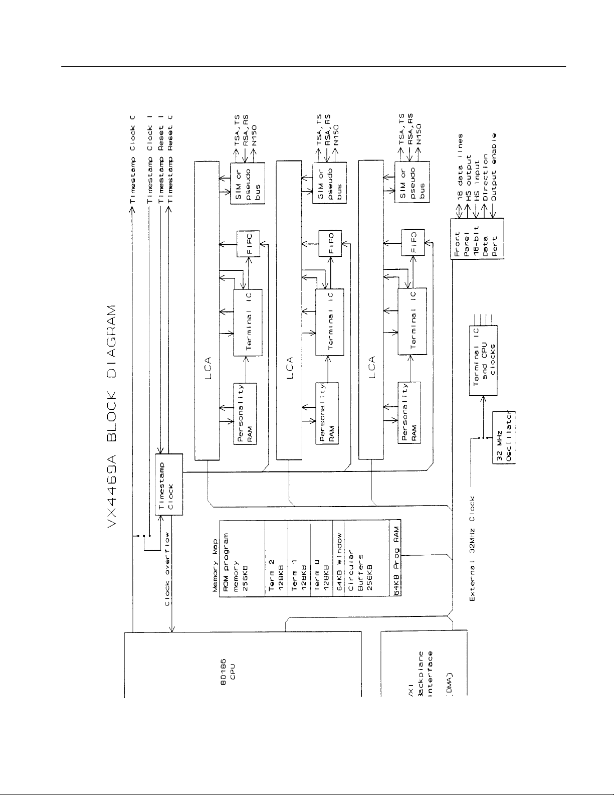
Product Description
This section begins with a brief description of the VX4469A, and then explains
how to configure and install the module in a VXIbus mainframe. Then you can
choose to perform the quick functional check, also included in this section, to
gain confidence that the instrument operates properly.
The VX4469A ARINC 629 Communication Module supports from one to three
ARINC 629 terminals. The standard board has one terminal. One or two
additional terminals are available as options. The VX4469A is designed to
transmit and receive data on ARINC 629 buses through a current (transformer)
coupling device that interfaces to the bus itself. Data to be transmitted is stored
in system memory shared by the terminal IC and an on-board 80186 processor.
The transmit schedule and system memory data locations are stored in a
Transmit Personality PROM (XPP). Data that is received is stored in the same
system memory. A Receive Personality PROM (RPP) and a Multiple Personality
PROM (MPP) contain information on which data to receive and where to store it
in the shared system memory.
Note that the VX4469A actually uses RAM instead of PROM for storing XPP,
RPP, and MPP information. All references to personality PROMs in this manual
are actually references to RAM locations.
Each ARINC 629 terminal on the VX4469A Module consists of:
H System memory shared by the VX4469A 80186 controller and each
terminal. It is used to store received data and data to be transmitted.
H A personality RAM that contains the information on what data to transmit
and receive and the data’s location in shared memory.
H A terminal protocol IC which interprets the personality PROM and translates
data to/from 16-bit shared memory words and Manchester bit serial
encoding.
H A Serial Interface Module (SIM) that modulates/demodulates the Manchester
coding and is intended to drive a current coupler on a twisted pair bus.
H An external trigger interface through the front panel and a VXI TTL trigger
interface through the backplane.
VX4469A ARINC 629 Communication Module User Manual
1–1
Page 24

Getting Started
NOTE. To help insure optimum ARINC 629 compatibility, each terminal uses the
VLSI Terminal IC and Serial Interface Module (SIM) technology developed by
Boeing.
A pseudo bus module that replaces the SIM and provides a voltage bus without
SIMs or current couplers is also available. Appendix G gives additional
information on the pseudo bus module.
The VX4469A allows you to program the Personality PROMs (RAMs) and to
read and write data from/to the shared memory.
The VX4469A also has two test modes. The test modes allow transmitting data
with Manchester, parity and timing errors as well as causing collisions on the
ARINC 629 bus.
Terminal Programmability
ARINC 629
Each terminal is software programmable for transmit interval, terminal gap, sync
gap, block/independent mode, and alternate mode. Each terminal may be
disabled individually. The three terminals may all be on the same bus or they
may be on two or three different busses. Terminals may also be configured to be
receive only.
The 32 MHz clock for the processor and terminal ICs may be provided externally to test external systems’ sensitivity to clock frequency. There are time stamp
clock and time stamp clock reset inputs and outputs to allow synchronizing time
on several systems.
ARINC 629 is a bit-serial, time-multiplexed, multiple-transmitter, data bus
developed for use primarily on certain commercial aircraft. All data transmitted
on the ARINC 629 bus consists of at least a label, followed by up to 256 16-bit
data words.
Data to be transmitted or received is placed in a terminal’s shared memory by an
on-board 80186 processor. The terminal IC uses a sophisticated built-in data
management scheme to read the personality PROM and manage transmission
and reception.
The basic unit of data transmission is a wordstring. A wordstring consists of a
label and between 0 and 256 data words. A given terminal is allowed to transmit
up to 31 wordstrings per transmission.
1–2
Protocol Timers
Each terminal determines when to transmit by using three timers and by
monitoring bus activity. The first timer, Transmit Interval, determines the
minimum amount of time a terminal waits between transmissions.
VX4469A ARINC 629 Communication Module User Manual
Page 25

Getting Started
The second timer, Sync Gap, is used to insure that all terminals can transmit
before any terminal re-transmits, and insures that there is a bus quiet time at least
Sync Gap long after each terminal has transmitted.
The third timer, Terminal Gap, determines which terminal transmits first if two
or more terminals’ Transmit Interval timers have elapsed and the bus is busy.
Modes
Transmit Schedules
The VX4469A supports both Periodic and Aperiodic modes. In Periodic mode,
the transmit interval time is longer than the time required for all terminals to
complete one transmission. In Aperiodic mode, after all terminals have transmitted, none will transmit again until there has been a bus quiet time of Sync
Gap. Thereafter the terminals will tend to transmit in Terminal Gap order,
shortest to longest.
A bus that is not fully loaded runs in Periodic mode, while a bus with terminals
transmitting more data than will fit in the transmit interval will automatically run
in Aperiodic mode. A bus will normally switch between Periodic and Aperiodic
modes as terminals have more or less data to transmit.
The order in which a terminal transmits data is determined by the contents of the
Transmit Personality PROM. The Transmit Personality PROM is a 31 row by 31
column arrangement in RAM and is fully user-programmable.
There are three modes of scheduling: Block, Independent and Alternate. In Block
mode, the wordstrings described in a single row are transmitted. Independent
mode transmits one wordstring from each column of the array. Alternate mode
can only be entered from Block mode. It is similar to Block mode with its first
row number defined in the first control cell. The terminal IC can be switched
back and forth between Block mode and Alternate mode while the bus is in
operation.
Fuses
BITE (Built-In Test
Equipment)
VX4469A ARINC 629 Communication Module User Manual
The VX4469A Module has 5 VDC and ±24 VDC fuses. The fuses protect the
module in case of an accidental shorting of the power bus or any other situation
where excessive current might be drawn.
If the +5 V fuse opens, the VXIbus Resource Manager will be unable to assert
SYSFAIL INHIBIT on this module to disable SYSFAIL*.
If any fuse opens, the fault must be removed before replacing the fuse. Refer to a
qualified service person for assistance.
Built in Test Equipment (BITE) uses regular data transmissions to check SIM
and coupler functionality, so as not to corrupt operation of the bus. The SIM
constantly monitors the wraparound path, including itself and the selected
channel. In addition, a special test function is available which selects and
monitors the spare coupler channel, and then reports the results. Visual BITE is
1–3
Page 26

Getting Started
provided for each terminal through a series of LEDs that indicate terminal active,
string active, receive error, transmit error, bus busy, and transmit enable. The
processor also has an LED indicating that an error has occurred, and another
LED is toggled on and off while the processor is idling, giving an indication of
how busy the processor is.
Binary Transfer
Accessories
Refer to Appendix J: Binary Transfer for information relating to National
Instruments GPIB-VXI/C Slot 0 modules.
Table 1–1 lists the standard accessories included with the VX4469A.
T able 1–1: Standard Accessories
Accessory Part Number
VX4469A User Manual 070-9147-XX
Table 1–2 lists the optional accessories for the VX4469A.
T able 1–2: Optional Accessories
Accessory Part Number
Adds one additional terminal VX4469A-01
Adds two additional terminals VX4469A-02
Pseudo-bus SIM See Appendix G for
information
1–4
VX4469A ARINC 629 Communication Module User Manual
Page 27
Getting Started
Figure 1–1: System Configuration
VX4469A ARINC 629 Communication Module User Manual
1–5
Page 28

Getting Started
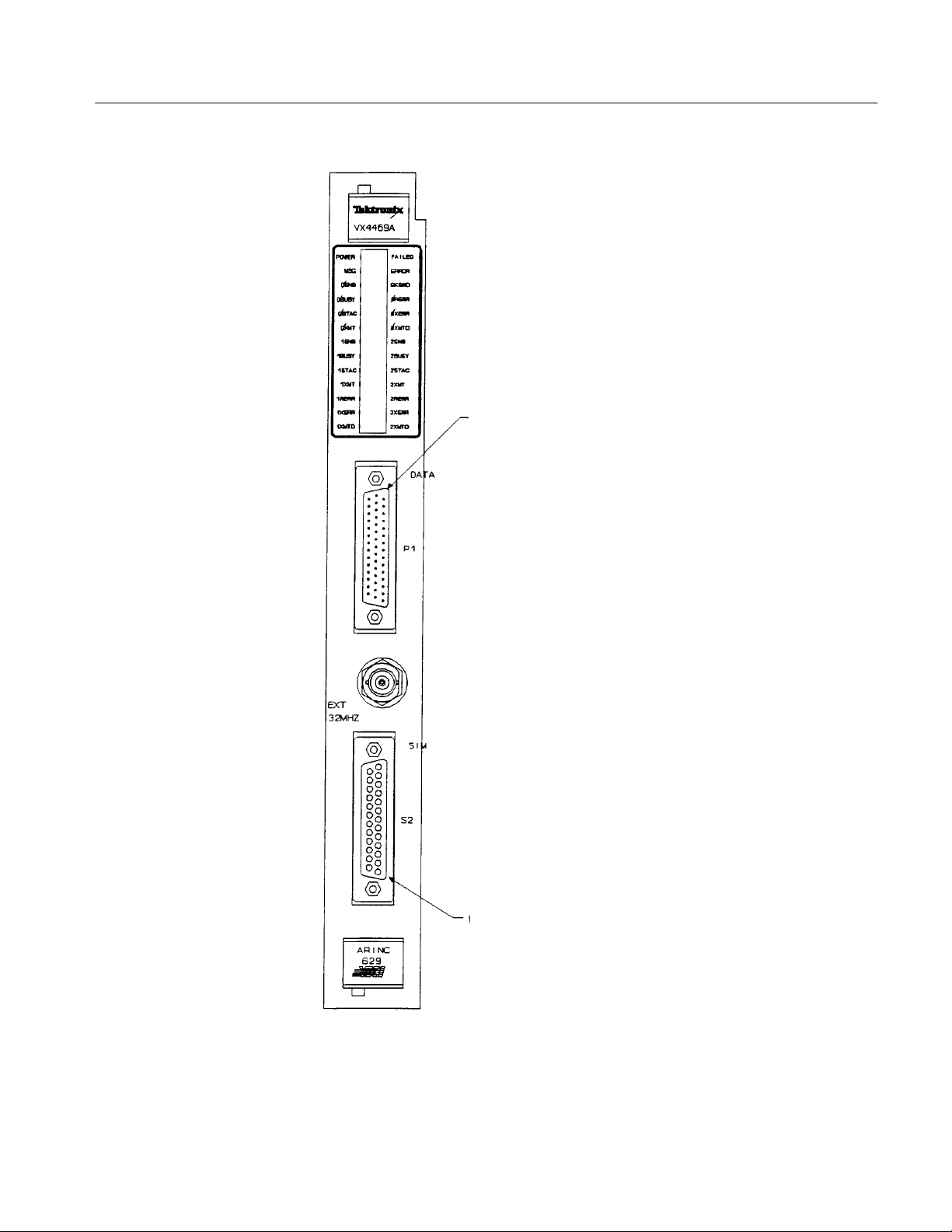
Controls And Indicators
The following controls and indicators are provided to select and display the
functions of the VX4469A Module’s operating environment. See Figures 1–2
and 1–3 for their physical locations.
Figure 1–2: VX4469A Controls and Indicators
Switches
1–6
The following switches must be correctly set to insure proper operation. See
Configuration for details of how to set the switches.
Logical Address Switches
VMEbus Interrupt Level Select Switch
Jumpers
VX4469A ARINC 629 Communication Module User Manual
Page 29
Pin 1
Getting Started
Pin 1
Figure 1–3: VX4469A Front Panel
VX4469A ARINC 629 Communication Module User Manual
1–7
Page 30

Getting Started
LEDs
Configuration
Logical Address Switches
The following LEDs are visible at the top of the VX4469A Module’s front panel
to indicate the status of the module’s operation. See Status and Events for a
description of each LED’s meaning.
Power LED
Failed LED
MSG LED
Error LED
Background LED
The following switches must be correctly set to insure proper operation. Refer to
Figure 2 for their physical locations.
Each function module in a VXIbus System must be assigned a unique logical
address, from 1 to 255 decimal. The base VMEbus address of the VX4469A is
set to a value between 1 and FFh (255d) by two hexadecimal rotary switches.
Align the desired switch position with the arrow on the module shield.
The actual physical address of the VX4469A Module is on a 64 byte boundary. If
the switch representing the most significant digit (MSD) of the logical address is
set to position X and the switch representing the least significant digit (LSD) of
the logical address is set to position Y, then the base physical address of the
VX4469A will be [(64d * XYh) + 49152d]. For example:
1–8
IEEE-488 Address
L.A. MSD LSD Base Physical Address (d)
Ah 0 A (64 * 10) + 49152 = 49792d
15h 1 5 (64 * 21) + 49152 = 50496d
where:
L.A. = Logical Address
MSD = Most Significant Digit
LSD = Least Significant Digit
Using the VX4469A Module in an IEEE-488 environment requires knowing the
module’s IEEE-488 address in order to program it. Different manufacturers of
IEEE-488 interface devices may have different algorithms for equating a logical
address with an IEEE-488 address. Consult the operating manual of the Resource
Manager/IEEE-488 Interface Module being used for additional information.
VX4469A ARINC 629 Communication Module User Manual
Page 31

Getting Started
If the VX4469A is being used in a MATE system, VXIbus logical addresses are
converted to IEEE-488 addresses using the algorithm specified in the MATE
IAC standard (MATE-STD-IAC). This algorithm is described in detail in the
73A-156 Operating Manual.
VMEbus Interrupt Level
Select Switch
Jumpers
Each function module in a VXIbus System can generate an interrupt on the
VMEbus to request service from the interrupt handler located on its commander.
When using the VX4469A with a Tektronix/CDS commander module, set the
interrupt level to the same level as the interrupt handler on that commander. The
VMEbus interrupt level on which the VX4469A Module generates interrupts is
set by a BCD rotary switch. Align the desired switch position with the arrow on
the module shield.
Valid Interrupt Level Select switch settings are 1 through 7, with setting 1
equivalent to level 1, etc. The level chosen should be the same as the level set on
the VX4469A’s interrupt handler, typically the module’s commander. Setting the
switch to an invalid interrupt level (0, 8, or 9) will disable the module’s
interrupts.
Interrupts are used by the module to return VXIbus Protocol Events to the
module’s commander. Refer to Operating Basics for information on interrupts.
The VXIbus Protocol Events supported by the module are listed in the Specifica-
tions.
J01 32 MHz Clock
1 2 3 (factory) selects internal 32 MHz clock for terminal ICs and processor.
1 2 3 selects external (front panel BNC connector) for 32 MHz clock.
J02 Time Stamp Clock
1
2 3 (factory) selects internally generated clock for time stamp.
1 2 3 selects external clock (front panel connector S2 pin 4) for time stamp.
Configure VXI TTL
Trigger Lines
VX4469A ARINC 629 Communication Module User Manual
The VXI TTL trigger lines are not configured at the factory. You may need to
jumper the trigger lines on J1401 to the VX4469A trigger inputs and outputs.
Refer to Figure 1–2 for the location of J1401.
The eight header pins marked VXI TTL Trigger Line 0 – 7 connect to the VXI
backplane VXI TTL Trigger Lines. The other eight header pins connect to the
terminal and software trigger inputs and outputs. Terminal and software trigger
lines may be connected to any of the backplane VXI TTL trigger lines. Refer to
Figure 1–4.
Refer to Appendix C: Trigger Lines for additional information regarding VXI
TTL Trigger lines.
1–9
Page 32

Getting Started
VXI TTL Trigger Line 0
VXI TTL Trigger Line 1
VXI TTL Trigger Line 2
VXI TTL Trigger Line 3
VXI TTL Trigger Line 4
VXI TTL Trigger Line 5
VXI TTL Trigger Line 6
VXI TTL Trigger Line 7
Terminal 0 VXI TTL Trigger Out
Terminal 1 VXI TTL Trigger Out
Terminal 2 VXI TTL Trigger Out
Software VXI TTL Trigger Out
Terminal 0 VXI TTL Trigger In
Terminal 1 VXI TTL Trigger In
Terminal 2 VXI TTL Trigger In
Software VXI TTL Trigger In
Figure 1–4: Trigger Lines
J1401
P2
1–10
VX4469A ARINC 629 Communication Module User Manual
Page 33

Installation
Getting Started
This section describes how to install the VX4469A.
Requirements And
Cautions
Tools Required
The VX4469A Module is a C size VXIbus instrument module and therefore may
be installed in any C or D size VXIbus mainframe slot other than slot 0. If the
module is being installed in a D size mainframe, consult the operating manual
for the mainframe to determine how to install the module in that particular
mainframe. Setting the module’s Logical Address switch defines the module’s
programming address. Refer to Configuration for information on selecting and
setting the module’s logical address.
The following tools are required for proper installation:
Slotted screwdriver set.
CAUTION. Note that there are two printed ejector handles on the module. To
avoid installing the card incorrectly, make sure the ejector marked “VX4469A”
is at the top.
In order to maintain proper mainframe cooling, unused mainframe slots must be
covered with the blank front panels supplied with the mainframe.
CAUTION. Verify that the mainframe is able to provide adequate cooling and
power with this module installed. Refer to the mainframe Operating Manual for
instructions.
If the VX4469A is used in a Tektronix/CDS VXIbus Mainframe, all VX4469A
cooling requirements will be met.
CAUTION. If the VX4469A Module is inserted in a slot with any empty slots to the
left of the module, the VME daisy-chain jumpers must be installed on the
backplane in order for the VX4469A Module to operate properly. Check the
manual of the mainframe being used for jumpering instructions.
VX4469A ARINC 629 Communication Module User Manual
1–11
Page 34

Getting Started
Installation Procedure
CAUTION. The VX4469A Module is a piece of electronic equipment and therefore
has some susceptibility to electrostatic damage (ESD). ESD precautions must be
taken whenever the module is handled.
1. Record the revision level, serial number (located on the label on the top
shield of the VX4469A), and switch settings on the Installation Checklist.
2. Verify that the switches are switched to the correct values.
3. Make sure power is off in the mainframe.
4. The module can now be inserted into one of the instrument slots of the
mainframe.
5. Cable Installation: Use a suitable cable to interface between the module I/O
connector and the Unit Under Test (UUT).
1–12
Figure 1–5: Module Installation
VX4469A ARINC 629 Communication Module User Manual
Page 35

Installation Checklist
Getting Started
Installation parameters will vary depending on the mainframe being used. Be
sure to consult the mainframe Operating Manual before installing and operating
the module.
Revision Level:
Serial No.:
Mainframe Slot Number:
Switch Settings:
VXIbus Logical Address Switch:
(FFh enables dynamic configuration.)
Interrupt Level Select Switch: Dynamically programmed by the Resource
Manager.
Cables Installed: (if any)
Performed by: _______________________ Date: _____________
VX4469A ARINC 629 Communication Module User Manual
1–13
Page 36

Getting Started
1–14
VX4469A ARINC 629 Communication Module User Manual
Page 37

Operating Basics
Page 38

Page 39

Operating Basics
Functional Check
The VX4469A Module will execute a self test at power-on, or upon direction of
a VXIbus hard or soft reset condition, or upon command. A VXIbus hard reset
occurs when another device, such as the VXIbus Resource Manager, asserts the
backplane line SYSRST*. A VXIbus soft reset occurs when another device, such
as the VX4469A’s commander, sets the Reset bit in the VX4469A’s Control
register.
At power-on, as well as during self test, all module outputs remain isolated from
the module’s front panel connector.
During a power-on, or hard or soft reset, the following actions take place:
1. The SYSFAIL* (VME system-failure) line is set active, indicating that the
module is executing a self test, and the Failed LED is lit. In the case of a soft
reset, SYSFAIL* is set. However, all Tektronix/CDS commanders will
simultaneously set SYSFAIL INHIBIT. This is done to prevent the resource
manager from prematurely reporting the failure of a card.
2. If the self test completes successfully, the SYSFAIL* line is released, and the
module enters the VXIbus PASSED state (ready for normal operation).
SYSFAIL* will be released within three seconds in normal operation.
If the self test fails, the SYSFAIL* line remains active (or is set active, in the
case of a commanded self test or soft reset), and the module makes an
internal record of what failure(s) occurred. It then enters the VXIbus
FAILED state, which allows an error message to be returned to the module’s
commander.
The default power-on setup and data is as follows:
current terminal is 0
all terminals are in independent mode (not block mode)
all terminals are in normal mode (not alternate mode)
all terminals are disabled
all terminals’ bus requests are enabled
all terminals’ transmit intervals (TI) are 0
all terminals’ terminal gaps (TG) are 0
all terminals’ sync gaps (SG) are 10
all terminals’ channel IDs are 0
all terminals’ serial interface module receive thresholds are 1000
the data radix is hex
the command parameter radix is decimal
the timestamp clock period (tick) is 10
microseconds
10
10
mv
VX4469A ARINC 629 Communication Module User Manual
2–1
Page 40

Operating Basics
the overload timer is 50010 milliseconds
the system interrupt on error is enabled
the system interrupt on vector instruction b, c, or f is enabled
all circular buffer definitions are erased
all instruction blocks are initialized to ’no instructions’ or ’done’
all vector indexes are set to instruction block 0
all terminal shared memory is initialized to 0s
all terminal personality PROM is initialized to 1s (ff hex)
all error messages are cleared from the error message queue
the error message format is set to normal
the VXI FHS active bit is disabled
the interrupt register is cleared
SYSFAIL* Operation
Functional Overview
SYSFAIL* becomes active during power-up, hard or soft reset, self test, or if the
module loses any of its power voltages. When the mainframe Resource Manager
detects SYSFAIL* set, it will attempt to inhibit the line. This will cause the
VX4469A Module to deactivate SYSFAIL* in all cases except when +5 volt
power is lost.
The VX4469A ARINC 629 Communication Module is programmed by ASCII
characters issued from the system controller to the VX4469A Module via the
module’s VXIbus commander and the VXIbus mainframe backplane. The
module is a VXIbus Message Based Device and communicates using the VXIbus
Word Serial Protocol. Refer to the manual for the VXIbus device that will be the
VX4469A Module’s commander for details on the operation of that device.
If the module’s commander is a Tektronix/CDS Resource Manager/IEEE-488
Interface Module, refer to that Operating Manual and the programming examples
in this manual for information on how the system controller communicates with
the commander being used.
The VX4469A ARINC 629 Communication Module supports from one to three
ARINC 629 terminals. The VX4469A is designed to transmit and receive data
on ARINC 629 buses through a current (transformer) coupling device that
interfaces to bus itself. Data to be transmitted is stored in system memory shared
by the Terminal IC and an on-board 80186 processor. The transmit schedule and
system memory data locations are stored in a Transmit Personality PROM
(XPP). Data that is received is stored in the same system memory. A Receive
Personality PROM (RPP) and a Multiple Personality PROM (MPP) contain
information on which data to receive and where to store it in the shared system
memory.
2–2
VX4469A ARINC 629 Communication Module User Manual
Page 41

Power-on
Operating Basics
Note that the VX4469A actually uses RAM instead of PROM for storing XPP,
RPP, and MPP information. All references to personality PROMs in this manual
are actually references to RAM locations.
If the VX4469A is read without first giving it a command that would return
information, it will return its default message of:
VX4469A TMx<cr><lf>
where x is the current default terminal. If the VX4469A has any errors in its error
queue, the default message will be:
VX4469A TMx ERRORS<cr><lf>
The VX4469A Module will complete its self test and be ready for programming
five seconds after power-on. The VXIbus Resource Manager may add an
additional one or two second delay. The MSG LED will blink during the
power-up sequence as the VXIbus Resource Manager addresses all modules in
the mainframe. The default condition of the module after power-on is described
in Functional Check.
VXIbus Basics
The VX4469A Module is a C size single slot VXIbus Message-Based Word
Serial instrument. It uses the A16, D16 VME interface available on the
backplane P1 connector and does not require any A24 or A32 address space. The
module is a D16 interrupter.
The VX4469A Module is neither a VXIbus commander or VMEbus master, and
therefore it does not have a VXIbus Signal register. The VX4469A is a VXIbus
message based servant.
The module supports the Normal Transfer Mode of the VXIbus, using the Write
Ready, Read Ready, Data In Ready (DIR), and Data Out Ready (DOR) bits of
the module’s Response register.
A Normal Transfer Mode read of the VX4469A Module proceeds as follows:
1. The commander reads the VX4469A’s Response register and checks if the
Write Ready and DOR bits are true. IF they are, the commander proceeds to
the next step. If not, the commander continues to poll these bits until they
become true.
2. The commander writes the Byte Request command (0DEFFh) to the
VX4469’s Data Low register.
VX4469A ARINC 629 Communication Module User Manual
2–3
Page 42

Operating Basics
3. The commander reads the VX4469A’s Response register and checks if the
Read Ready and DOR bits are true. If they are, the commander proceeds to
the next step. If not, the commander continues to poll these bits until they
become true.
4. The commander reads the VX4469A’s Data Low register.
A Normal Transfer Mode Write to the VX4469A Module proceeds as follows:
1. The commander reads the VX4469A’s Response register and checks if the
Write Ready and DIR bits are true. If they are, the commander proceeds to
the next step. If not, the commander continues to poll the Write Ready and
DIR bits until they are true.
2. The commander writes the Byte Available command which contains the data
(0BCXX or 0BDXX, depending on the End bit) to the VX4469A’s Data Low
register.
The VX4469A Module has a register beyond those defined for VXIbus message
based devices. This register may be used for 16 bit data transfers between the
VXI backplane and the terminal shared memory. Any attempt by another module
to read or write to any undefined location of the VX4469A’s address space may
cause incorrect operation of the module.
VX4469A VXI Registers
As with all VXIbus devices, the VX4469A Module has registers located within a
64 byte block in the A16 address space.
The base address of the VX4469A device’s registers is determined by the
device’s unique logical address and can be calculated as follows:
Base Address = V * 40H + C000H
where V is the device’s logical address as set by the Logical Address switches.
Below is a list of the VX4469A VXI registers with a complete description of
each. In this list, RO = Read Only, WO = Write Only, R = Read, and W = Write.
The offset is relative to the module’s base address.
T able 2–1: Register Definitions
Register Address Type Value (Bits 15-0)
ID Register 0000H RO 101 1 1111 1 111 1100 (BFFCh)
Device Type 0002H RO See Device Type definition below
Status 0004H R Defined by state of interface
Control 0004H W Defined by state of interface
2–4
Offset 0006H WO Not used
VX4469A ARINC 629 Communication Module User Manual
Page 43

Operating Basics
T able 2–1: Register Definitions (Cont.)
Register Value (Bits 15-0)TypeAddress
Protocol 0008H RO 1111 0111 1111 1111 (F7FFh)
Response 000AH RO Defined by state of the interface
Data High 000CH Not used
Data Low 000EH W See Data Low definition below
Data Low 000EH R See Data Low definition below
Data Transfer 0020H RW See GRD and GWD commands.
Word Serial Commands
VX4469A Interrupts
A write to the Data Low register causes this module to execute some action
based on the data written. The device-specific Word Serial command this module
responds to and the result of this command is:
Command Response
Read Protocol FE6Bh
The VX4469A will interrupt its commander with the following “event” either if
the error interrupt is enabled (SSEE command) and an error is added to the error
queue, or if vector interrupts are enabled (SSVE command) and a vector function
b, c or f occurs.
Request True:
1514131211109876543210
11111101<--Logical Address--->
VX4469A ARINC 629 Communication Module User Manual
2–5
Page 44

Operating Basics
ARINC 629
Each ARINC 629 terminal on the VX4469A Module consists of the following:
H System memory shared by the VX4469A 80186 controller and each
terminal. It is used to store data to be transmitted and received.
H A personality PROM (RAM) that contains the information on what data to
transmit and receive and the data’s location in shared memory.
H A terminal protocol IC which interprets the personality PROM (RAM) and
translates data to/from 16-bit shared memory words and Manchester bit
serial encoding.
H A Serial Interface Module (SIM) that modulates/demodulates the Manchester
coding and is intended to drive a current coupler on a twisted pair bus.
All data transmitted on the ARINC 629 bus consists of at least a label. Zero to
256 16-bit data words follow a label.
Protocol Timers
Data to be transmitted is placed in a terminal’s shared memory by the 80186
processor. The terminal IC reads the transmit portion of the Personality PROM
(RAM) to determine what labels to transmit and where the data, if any, to be
transmitted with each label is located in shared memory.
Data to be received and where to place it in shared memory is determined by the
terminal IC reading the receive and multiple personality portions of the
Personality PROM (RAM). The 80186 can then read the received data from
shared memory.
Each terminal determines when to transmit by using three timers and monitoring
bus activity. The first timer is the Transmit Interval and should be the same for
all terminals on the bus. It determines the minimum amount of time a terminal
waits between transmissions. This timer is reset as soon as the terminal begins to
transmit and counts to completion independent of what happens on the bus.
The second timer is the Sync Gap. The sync gap time is the same for each
terminal on the bus. The sync gap is used to insure that all terminals have a turn
to transmit before any terminal re-transmits. The Sync Gap timer is reset when
the terminal begins to transmit. Until it counts to completion, any bus activity
will reset it again. Once it has counted to completion, it will not reset again until
the terminal transmits again. This insures that there is a bus quiet time at least
Sync Gap long after each terminal has transmitted before that terminal transmits
again.
2–6
VX4469A ARINC 629 Communication Module User Manual
Page 45

Modes
Operating Basics
The third timer is the Terminal Gap. The terminal gap time is different for each
terminal on the bus, and determines which terminal transmits first if two or more
terminals’ Transmit Interval timers have elapsed and the bus is busy. The
Terminal Gap timer is reset with any bus activity and will count only after the
Sync Gap timer has completed. The terminal will transmit after the Transmit
Interval timer and Terminal Gap timer have counted to completion. If two or
more terminals’ Transmit Interval and Sync Gap timers have completed, the
terminal with the shortest Terminal Gap will transmit next. All terminals’
Terminal Gap times are shorter than the common Sync Gap time.
Periodic Mode
Aperiodic Mode
A bus that is not fully loaded runs in Periodic mode. In this mode, the transmit
interval time is longer than the time required for all terminals to complete one
transmission. After a terminal transmits, the Transmit Interval timer begins to
count. Before the Transmit Interval timer completes, there will be a quiet time on
the bus at least Sync Gap long so the Sync Gap timer will have counted to
completion. If another terminal is not transmitting when the transmit interval
completes, the terminal gap timer will have completed also and the terminal will
transmit as soon as its transmit interval has completed. What normally happens
is that all the terminals tend to creep up behind the terminal with the slowest
clock. In this condition, the terminals are not transmitting in any particular order
but each one is separated from the previously transmitting terminal by its
terminal gap. The first one transmitting will be the one with the slowest clock.
A bus with terminals transmitting more data than will fit in the transmit interval
will automatically run in Aperiodic mode. In this mode, after all terminals have
transmitted, none will transmit again until there has been a bus quiet time of
Sync Gap. Thereafter the terminals will tend to transmit in Terminal Gap order,
shortest to longest.
A bus may normally switch between Periodic and Aperiodic modes as terminals
have more or less data to transmit.
Instrument I/O
Transmit Schedules
VX4469A ARINC 629 Communication Module User Manual
The basic unit of data transmission is a wordstring. A wordstring consists of a
label and between 0 and 256 data words. A terminal is allowed to transmit up to
31 wordstrings per transmission. The order in which a terminal transmits data is
determined by the transmit portion of its personality PROM. The transmit
personality PROM is divided into a 31 by 31 array of cells each eight bytes long.
2–7
Page 46

Operating Basics
Each cell describes a wordstring to transmit, the label, data address in shared
memory and data length.
There are three modes of scheduling: Block, Independent and Alternate. These
modes are controlled by a VX4469A Control register driving input pins on the
terminal IC.
In Block mode, the wordstrings described in a single row are transmitted. A row
counter is incremented with each transmission. The row counter is reset when it
becomes larger than maximum row value (y modulo) stored in the first control
cell located in the 32nd row of the array.
Independent mode transmits one wordstring from each column of the array. Each
column may have a different number of wordstrings defined. The number for
each column (y modulo) is defined in the control cell in the 32nd row of that
column. There is a separate row counter for each column. When the y modulo
row of each column is reached, its row counter is reset to 0.
Alternate mode can only be entered from Block mode. It is intended that the
terminal IC can be switched back and forth between Block mode and Alternate
mode while the bus is in operation. The schedule cells for Alternate mode are
located in the last rows of the 31 by 31 array. It is similar to Block mode with its
first row number defined in the first control cell. Alternate schedule is transmitted one row of wordstrings at a time until the row defined in the 31st row of
the array. This last row is repeated until the terminal IC is returned to Block
mode.
Hardware CRC
Receive Interrupt Vectors
and Label Extension
The VX4469A also has hardware capability for generating CRCs on transmitted
wordstrings. The CRC hardware reads the label and data at the same time the
terminal IC does. The CRC hardware calculates the CRC and supplies the CRC
word to the terminal IC at the time the terminal IC is reading the last word of the
wordstring. The CRC hardware works with the terminal IC and does not require
any bus time from the 80186. The VX4469A also has hardware CRC verification
on receive data.
When an ARINC 629 terminal transmits a wordstring, the first word of that
wordstring is its label. The high four bits of this label word is called the label
extension. The label extension is the channel ID of the terminal transmitting the
wordstring.
When a terminal receives a wordstring, it can optionally generate an interrupt
vector. You can program the VX4469A to use this interrupt vector number for a
variety of functions, including storing in FIFO memory the interrupt vector
number and a timestamp.
2–8
VX4469A ARINC 629 Communication Module User Manual
Page 47

Operating Basics
The terminal IC does not use the label extension when it generates an interrupt
vector. Therefore the interrupt vector generated when a label is received is
independent of the channel ID of the transmitter.
The VX4469A, under program control, can substitute the label extension for the
low four bits of the late interrupt vector. This allows you to easily differentiate
between terminals transmitting the same label with different channel IDs. The
VX4469A also can return to the user the label extension with timestamp data.
Transmit Channel ID
Memory Switching
The VX4469A can enable a terminal to use a Channel ID stored in the high four
bits of an Xpp label field, instead of the channel ID set with the SC command.
This allows a single terminal to simulate multiple terminals with different
channel IDs.
The terminal IC reads and writes data from and to shared memory. The
VX4469A uses memory switching to insure that data in shared memory is not
partially overwritten by the terminal IC or user while the other is reading it.
Each terminal has its own 64 Kwords of shared memory. When the shared
memory for a terminal is normal, addresses or locations in the shared memory
are the same for both the terminal IC and commands such as RD and WD. When
memory is switched, the high order addressing bit is inverted for only the
terminal IC. This causes a terminal IC which is normally programmed to read
and write in the lower 32 Kwords of its shared memory to now read and write in
the upper 32 Kwords.
Thus you can examine and modify data in half the shared memory while the
terminal IC is operating out of the other half. You can then request a memory
switch and examine and modify new data. Switching automatically happens
between wordstrings.
A second memory switching mode switches the memory address for the terminal
IC in the low half of shared memory to the high half. Address in the high half of
memory are not switched. This makes it convenient to use circular buffers with
data always found in the high half and also to examine/change other data using
memory switching.
VX4469A ARINC 629 Communication Module User Manual
2–9
Page 48

Operating Basics
2–10
VX4469A ARINC 629 Communication Module User Manual
Page 49

Syntax and Commands
Page 50

Page 51

Command Syntax
Command protocol and syntax for the VX4469A Module are as follows:
1. Each command is terminated by a semicolon or a line feed.
2. White space characters (including space, tab, and carriage return) are
3. Non-printing characters are indicated by the following:
4. Characters may be sent as either upper or lower case.
5. Comments may be added to commands and will be ignored by the
ignored.
<cr> carriage return.
<lf> line feed.
<tm> terminator, either a linefeed or semicolon.
VX4469A. Begin the comment with an ! and end the command with a
terminator. The ! must not be in the middle of a command, but may be
placed after a line feed or semi-colon.
6. In the command descriptions, the following conventions have been used:
Brackets [ ] are used to show optional parts of commands.
Parts of commands enclosed in parenthesis ( ) contain two or more choices,
one of which must be used.
Lower case letters are used to represent numeric values. The descriptions
following the commands describe the use and range of these numbers.
VX4469A ARINC 629 Communication Module User Manual
3–1
Page 52

Command Syntax
3–2
VX4469A ARINC 629 Communication Module User Manual
Page 53

Functional Command Groups
This section lists the VX4469A commands by functional command group.
System Commands
These low-level commands are typically sent by the module’s commander,
transparent to the user of the module. An exception is the Read Status command,
which is sent whenever a Serial Poll on an IEEE-488 system is performed. Most
commanders or Slot 0 devices have specific ASCII commands which will cause
them to send one of these low-level commands to a specified instrument. Refer
to the Operating Manual of the commander or Slot 0 device for information on
these commands.
Command Effect
Clear The module clears its VXIbus interface and any pending commands.
Current module operations are unaffected.
Begin Normal
Operation
Read Protocol The module will return its protocol to its commander.
Read Status The module will return its VXI status byte to its commander.
Set Lock Set the Lock bit of the Response register.
Clear Lock Clears the Lock bit of the Response register.
Read Interrupters Returns the value FFF9, indicating there is one interrupter on this
Read Interrupt Line Returns the interrupt line per VXI Specification.
Asynchronous Mode
Control
Abort Normal
Operation
End Normal
Operation
Control Event Used by a commander to selectively enable the generation of events
Read Protocol Error Returns the module’s most recent error code, which includes multiple
Byte Available Transfers module commands to this module.
The module will begin operation per VXI Specification.
module.
Returns information that events are being sent as interrupts per VXI
Specification.
Causes this device to cease normal operation per VXI Specification.
Causes this device to cease normal operation per VXI Specification.
by a servant.
query errors, unsupported commands, and DOR violations.
Byte Request Requests data be returned form the module.
VX4469A ARINC 629 Communication Module User Manual
3–3
Page 54

Functional Command Groups
Module Commands
Command Summary
Command Effect
Control Response Returns information indicating response interrupts are not supported.
Trigger This module will accept the Trigger command, although no part of this
instrument will be affected by it.
A summary of the VX4469A Module’s commands is listed below. This is
followed by detailed descriptions of each of the commands. A sample BASIC
program using these commands is shown in the Programming Examples section.
Detailed descriptions of each command (in alphabetical order) are given
following the summary. An overview of the commands is as follows:
Command Description
BR binary read:
BRC circular buffer BRG registers
BRD data BRM multiple PP
BRR receive PP BRX transmit PP
BW binary write:
BWC circular data BWD data
BWM multiple PP BWR receive PP
BWX transmit PP
CC clear circular buffer data.
CCA clear all circular buffers of data.
CF clear a specified terminal’s hardware FIFO.
DC define circular buffer.
F fill the Personality PROM (RAM) for a specified terminal with all ones
(FF hex), or fills shared memory with zeros.
GRD supply data to the 16-bit register on the VXI backplane.
GWD accept data via the 16-bit register on the VXI backplane.
HN switch this terminal’s memory addressing to normal at the beginning of
the next wordstring transmitted or received by this terminal.
3–4
HPN switch this terminal’s memory addressing to normal at the beginning of
the next wordstring transmitted by this terminal whose transmit cell in
the Xpp has the Switch bit true.
VX4469A ARINC 629 Communication Module User Manual
Page 55

Functional Command Groups
Command Description
HPS switch this terminal’s memory addressing to switched at the beginning
of the next wordstring transmitted by this terminal whose transmit cell
in the Xpp has the Switch bit true.
HR reset this terminal’s memory addressing to normal immediately. If it is
already in normal, this command has no effect.
HS switch this terminal’s memory addressing to switched at the beginning
of the next wordstring transmitted or received by this terminal.
IA initialize module to power-up, except power-up ROM.
IC initialize circular buffer definitions.
IM reset module to power-up state and then program it to record in circular
buffer 0 all labels with timestamps that are being transmitted on a bus.
IN initialize and monitor all terminals.
IVI initialize vector instructions.
IVX initialize vector index table.
LC list circular buffer status.
LCB list circular buffer status in binary format.
LE set up the VX4469A to return any error messages in its error queue.
LG set up the VX4469A to return the current value of the high 4 bits of
terminals currently in Test Mode.
LH list memory switch status.
LP set up the VX4469A to return the contents of the power-up PROM.
LR list revision.
LS set up the VX4469A to send back information about its setup.
LVI set up the VX4469A to return the instructions in a particular instruction
block.
LVX set up the VX4469A to return vector index information.
NRD front panel data port read data.
NWD front panel data port write data.
RC read circular buffer.
RCC read circular buffer, calculating and appending a CRC, using the
circular buffer cell size as the ’number of data words’ in the wordstring.
RCV read circular buffer variable, calculating and appending a CRC, using
the first data word in the circular buffer cell or the cell size, whichever is
less, as the ’number of data words’ in the wordstring.
RD read data from terminal’s shared memory.
RDC read data from shared memory, calculating and appending a CRC.
VX4469A ARINC 629 Communication Module User Manual
3–5
Page 56

Functional Command Groups
Command Description
RDV read data variable from shared memory , calculating and appending a
CRC, using the word at ’addr’ in shared memory as the ’number of
words’ in the wordstring.
RG read terminal IC’s status registers.
RI read interrupt status.
RM read Multiple Personality PROM (RAM).
RR read Receive Personality PROM (RAM).
RS read Serial Interface Module status.
RX read Transmit Personality PROM (RAM).
SBD disable the terminal IC from accessing the shared memory.
SBE enable the terminal IC to access the shared memory.
SC set the terminal ID for transmit data and receive data channeling.
SCL set the Channel ID to use or not use the Xpp label field for the channel
ID.
SD disable the specified terminal(s).
SE enable the specified terminal(s).
SFB set error message format to brief.
SFN set error message format to normal.
SH set the memory switch mode.
SI set the ARINC 629 parameters TI (transmit internal), TG (terminal gap),
and SG (sync gap).
SKD disables VXI TTL trigger, External trigger or label enables on a terminal
in test mode 2.
SKI causes a terminal in test mode 2 to transmit immediately.
SKL causes a terminal in test mode 2 to transmit after it receives a
particular label.
SKV causes a terminal in test mode 2 to transmit after it receives a VXI TTL
trigger.
SKX causes a terminal in test mode 2 to transmit after it receives an
external trigger.
SMA set the alternate mode pin on the terminal IC true.
SMB set the protocol transmit mode to block.
SMI set the protocol transmit mode to independent.
3–6
SMN set the alternate mode pin on the terminal IC false. This command
allows switching the terminal IC from alternate mode to block mode.
SO set overload timer value.
VX4469A ARINC 629 Communication Module User Manual
Page 57

Functional Command Groups
Command Description
SQVE enable/disable setting the terminal VXI trigger on a communication
error.
SQVG enable/disable setting the terminal VXI trigger on beginning to transmit.
SQVI enable/disable setting the terminal VXI trigger on interrupt vector bit 13.
SQVR enable/disable setting the terminal VXI trigger on interrupt vector bit 13
when this terminal has just received a wordstring that does not have a
valid CRC.
SQXE enable/disable setting the terminal VXI trigger on a communication
error.
SQXG enable/disable setting the terminal VXI trigger on beginning to transmit.
SQXI enable/disable setting the terminal VXI trigger on interrupt vector bit 13.
SQXR enable/disable setting the terminal VXI trigger on interrupt vector bit 13
when this terminal has just received a wordstring that does not have a
valid CRC.
SR set the radix of numeric data or command parameters.
SSE set system error interrupt.
SST set receive threshold.
SSV set system vector interrupt.
ST sets the time-stamp clock period.
SVI set up a list of commands to be executed whenever a particular vector
or vectors is/are generated.
SVX set which instruction block is to be used by each vector.
SW set the terminal to timestamp the end of a wordstring.
SXD set data transfer to disable VXI fast handshake protocol.
SXE set data transfer to enable VXI fast handshake protocol.
TQV test a terminal’s VXI TTL trigger.
TQX test a terminal’s external trigger.
TQSV test the VX4469A’s software VXI TTL trigger.
TQSX test the VX4469A’s software external trigger.
TS test SIM.
URM a user friendly way of reading data from the Multiple Personality
PROM.
URR a user friendly way of reading data from the Receive Personality
PROM.
URX a user friendly way of reading data from the Transmit Personality
PROM.
UWM a user friendly way of writing data to the Multiple Personality PROM.
VX4469A ARINC 629 Communication Module User Manual
3–7
Page 58

Functional Command Groups
Command Description
UWR,f a user friendly way of writing data to the Receive Personality PROM.
UWX,c,f a user friendly way of writing data to the Transmit Personality PROM.
WC write data to a cell in a circular buf fer.
WCC write data to a circular buffer, calculating, and appending a CRC.
WD write data to a terminal’s shared memory.
WDC write data, calculating and appending a CRC, to shared memory
starting at ’addr’, including ’label’ in the CRC calculation.
WM writes Multiple Personality PROM.
WR writes Receive Personality PROM.
WX writes Transmit Personality PROM.
All commands must end with a terminator <tm>, which may be a line feed <LF>
or semi-colon. White space characters are ignored.
The optional [U] (user friendly) and [B] (binary) parameters are mutually
exclusive. A command can not use both of these parameters at the same time.
The following summary shows the commands grouped according to function,
and may be useful as a quick reference guide.
3–8
VX4469A ARINC 629 Communication Module User Manual
Page 59

(t) terminal number prefix valid for all commands
(G) use 16-bit register
(U) user friendly prefix valid for some commands, not for use with (B)
(B) binary prefix valid for some commands, not for use with (U)!!
(N) front panel prefix, valid for some commands.
CT current terminal
Read
(B)RC read circular buffer
RCC read circular buffer CRC
RCV read circular buffer CRC variable
(G)RD read data to 16-bit register
(t)(B)RG read CT’s registers
(t)(N)(B)RD read CT’s data
(t)RDC read CT’s data CRC
(t)RDV read CT’s data CRC variable
(t)(U,B)RR read CT’s receive PP
(t)(U,B)RX read CT’s transmit PP
(t)(U,B)RM read CT’s multiple PP
(t)RI read interrupt status
Write
(B)WC write circular buffer
WCC write circular buffer CRC
(G)WD accept data via 16-bit register
(t)(B)(N)WD write CT’s data
(t)WDC write CT’s data with CRC
(t)(U,B)WR write CT’s receive PP
(t)(U,B)WX write CT’s transmit PP
(t)(U,B)WM write CT’s multiple PP
List
LC list circular buffer status
LE list error queue
LG list high 4 bits of terminals currently in Test Mode
LH list memory switch status
LS list module’s setup
LVI list vector instructions
LVX list vector index
LR list revision
Set
(t)SBD set CT’s instrument bus disable
(t)SBE set CT’s instrument bus enable
(t)SC set CT’s channel ID
(t)SCL use or not use Xpp label field
(t)SD set CT disable
SDA set all terminals disable
(t)SE set CT enable
SEA set all terminals enable
SFB set error message format to brief
SFN set error message format to normal
SHO set memory switch to OR mode
SHS set memory switch to invert mode
(t)SI set CT’s intervals (ti,tg,sg)
(t)SKD set kollision disable
(t)SKI set kollision immediate
(t)SKL set kollision label
(t)SKV set kollision VXI TTL
(t)SKX set kollision external
Functional Command Groups
(t)SMA set CT’s mode to alternate
(t)SMB set CT’s mode to block
(t)SMI set CT’s mode to independent
(t)SMN set CT’s mode to not alternate
SO set overload timer value
SRDD set data radix to decimal
SRDH set data radix hexadecimal
SRCD set command radix to decimal
SRCH set command radix to hexadecimal
SSE set system error interrupt
SST set receive threshold
SSV set system vector interrupt
ST set timestamp period
SVI set vector instructions
SVX set vector index
SXD set data transfer to disable VXI fast handshake protocol.
SXE set data transfer to enable VXI fast handshake protocol.
Fill
(t)FR fill CT’s receive PP with 1s
(t)FX fill CT’s transmit PP with 1s
(t)FM fill CT’s multiple PP with 1s
(t)FD fill CT’s shared memory with 0s
(t)FP fill CT’s PP with 1s
(t)FA fill CT’s PP with 1s and shared memory with 0s
Clear
CC clear circular buffer
CCA clear all circular buffers
(t)CF clear CT’s hardware FIFO
CFA clear all terminals’ hardware FIFO
Define
DC define circular buffer
Initialize
IA initialize all
IC initialize circular buffer definitions
IM initialize and record timestamped transmitting labels
IVI initialize vector instruction cells
IVX initialize vector index table
Test
(t)TS test SIM
Memory Switch
(t)HN switch memory addressing to normal
(t)HS switch memory addressing to switched
(t)HR reset memory addressing to normal
(t)HPN switch memory addressing to normal
(t)HPS switch memory addressing to switched
VX4469A ARINC 629 Communication Module User Manual
3–9
Page 60

Functional Command Groups
3–10
VX4469A ARINC 629 Communication Module User Manual
Page 61

Command Descriptions
Detailed descriptions of the VX4469A Module’s commands, in alphabetical
order, are listed on the following pages.
NOTE. All numbers in these descriptions are hexadecimal unless otherwise
indicated.
The radix for data and command parameters both to and from the module are
determined by the set radix commands, SRxx. The radix for data or parameters
sent to the module may be modified for a particular number by preceding that
number with a % character for decimal or # character for hexadecimal. For
instance, if the write data to shared PROM is used, and the current radix for both
data and command parameters is hex, decimal numbers may be included as
follows:
WD,100,7,8,9,%10,B,C,%13,E
Or, if the data and command parameters are decimal, hex numbers may be
included as follows:
WD,#100,7,8,9,10,#B,12,#D,13
Some of the commands, such as RD (read data) or SE (set enable), are terminal
dependent. A terminal is selected by specifying a terminal number. If the board is
a 3-terminal board, the number may be 0, 1, or 2. Any command may be
prefixed with a terminal number, or a terminal may be selected by the terminal
number followed by a terminator character. Until a different terminal number is
specified, all terminal-specific commands will refer to the previously selected
terminal. The currently selected terminal is indicated in the default readback
message.
VX4469A ARINC 629 Communication Module User Manual
3–11
Page 62

Command Descriptions
BRC
Syntax
Purpose
Description
Example
BRC,circular buffer number,number of words<tm>
Read circular buffer, binary. Sets the VX4469A to return data from a circular
buffer in binary data format.
circular buffer number is 0 to 0f
number of words is 0 to 07fff (32,767 decimal).
If the number of words requested is greater than the number in one cell, other
cells will be read and returned until the number is satisfied. If the number of
words requested is zero, the VX4469A will return data forever. This command
may be canceled before completion by sending another command.
Once the data is completely read from a cell, that cell is erased.
The data is returned as two 8-bit binary characters per word, with the least
significant bits of each word first. Binary mode uses no delimiters between data
words or circular buffer cells.
BRC,3,23<tm>
sets up the VX4469A to return data from circular buffer 3 until 23 words have
been read. If circular buffer 3 has no full cells, the system controller will be held
off until data is available. If the remainder of 23 divided by circular buffer 3’s
cell size is not zero, the last partial cell read will not be deleted from the circular
buffer.
3–12
VX4469A ARINC 629 Communication Module User Manual
Page 63

BRD
Command Descriptions
Syntax
Purpose
Description
Example
[t]BRD,start address,number of words<tm>
The Binary Read Data command reads data from the current terminal’s shared
memory.
[t] an optional terminal number, which must be either 0, 1, or 2. If omitted,
the last value specified is used.
start address Note that the addressing in the shared memory space is by 16-bit word
and not by byte.
number of words is 0 to 07fff (32,767 decimal).
The data is returned as two 8-bit binary characters per word, with the least
significant eight bits of each word first. Binary mode uses no delimiters between
data words.
2BRD,100,5<tm>
reads five words of data from terminal 2, beginning at shared memory address
100.
VX4469A ARINC 629 Communication Module User Manual
3–13
Page 64

Command Descriptions
BRG
Syntax
Purpose
Description
[t]BRG<tm>
The Binary Read Registers command sets up the VX4469A to read and return
the contents of the terminal IC’s internal registers in binary format.
[t] an optional terminal number, which must be either 0, 1, or 2. If omitted,
the last value specified is used.
The three registers are read at the time data is requested from the VX4469A.
They are read one at a time, so it is possible that the registers will change while
being read.
Six binary bytes are returned in the order shown, with the least significant byte
of each word first:
aaaa,bbbb,cccc<cr><lf>
where aaaa is the Error register, bbbb is the last word monitor, and cccc is the
Interrupt Vector register.
The Error register bits are as follows:
fedcba9876543210
||||||||||||||||_impersonate
||||||||||||||__|__op mode
|||||||||||||__short string
||||||||||||__parity error
|||||||||||__receive error flag
||||||||||__nobusa, write
|||||||||__nobusa, read
||||||||__pamerror - tg,sg
|||||||__pamerror - ti
| | | |__|__|__ transmit monitor errors (encoded)
| | |__ transmit error flag
| |__ transmitter enable
|__ string error
The last word monitor register contains the last label or data word sent for a
transmit operation and the last label word received for a receive operation.
The interrupt vector register (IVR) contains the 15-bit interrupt vector for the
current received or transmitted wordstring. The most significant bit of the IVR
contains the string error bit. The IVR makes available the value of the current
3–14
VX4469A ARINC 629 Communication Module User Manual
Page 65

Command Descriptions
interrupt vector at any time whether or not the Personality PROMS have been
programmed to provide interrupt vector strobes.
VX4469A ARINC 629 Communication Module User Manual
3–15
Page 66

Command Descriptions
BRM
Syntax
Purpose
Description
Example
[t]BRM,start address,number of bytes<tm>
The Binary Read Multiple command reads the Multiple Personality PROM in
binary format.
[t] an optional terminal number, which must be either 0, 1, or 2. If omitted,
the last value specified is used.
start address Note that the addressing in the Personality PROM space is by 8-bit
byte. The terminal must be disabled to read or write its personality
PROM.
number of bytes from 1 to 10,000.
The data is returned as one 8-bit binary character per byte. Binary mode uses no
delimiters between data bytes.
0BRM,0,100<tm>
sets up to read back 100 bytes of terminal 0 Multiple Personality PROM in
binary format, starting at address 0.
3–16
VX4469A ARINC 629 Communication Module User Manual
Page 67

BRR
Command Descriptions
Syntax
Purpose
Description
Example
[t]BRR,start address,number of bytes<tm>
The Binary Read Receive command reads the Receive Personality PROM in
binary format.
[t] an optional terminal number, which must be either 0, 1, or 2. If omitted,
the last value specified is used.
start address Note that the addressing in the Personality PROM space is by 8-bit
byte. The terminal must be disabled to read or write its personality
PROM.
number of bytes from 1 to 10,000.
The data is returned as one 8-bit binary character per byte. Binary mode uses no
delimiters between data bytes.
0BRR,200,10<tm>
sets up to read back 10 bytes of terminal 0 Receive Personality PROM in binary
format, starting at address 200.
VX4469A ARINC 629 Communication Module User Manual
3–17
Page 68

Command Descriptions
BRT
Syntax
Purpose
Description
Example
[t]BRT,segment,start address,number of bytes<tm>
The Binary Read Test Ram command sets up the VX4469A to return the
contents of the current terminal’s Test Ram in binary format.
[t] an optional terminal number, which must be either 0, 1, or 2. If omitted,
the last value specified is used.
segment Test Ram segment.
start address the byte address within the Test Ram segment.
Note that the addressing in the Test Ram space is by 8-bit byte. The terminal
must be in Test Mode and disabled to read or write its Test Ram.
The data is returned as one 8-bit binary character per byte. Binary mode uses no
delimiters between data bytes. If the user continues to read after “number of
bytes” bytes, the VX4469A will return space,<cr>,<lf> characters.
0BRT,2,0,10<tm>
sets up to read back 10 bytes of terminal 0 Test Ram starting at segment 2
address 0 in binary format.
3–18
VX4469A ARINC 629 Communication Module User Manual
Page 69

BRX
Command Descriptions
Syntax
Purpose
Description
Example
[t]BRX,start address,number of bytes<tm>
The Binary Read Xmit command reads the Transmit Personality PROM in
binary format.
[t] an optional terminal number, which must be either 0, 1, or 2. If omitted,
the last value specified is used.
start address Note that the addressing in the Personality PROM space is by 8-bit
byte. The terminal must be disabled to read or write its personality
PROM.
number of bytes from 1 to 10,000.
The data is returned as one 8-bit binary character per byte. Binary mode uses no
delimiters between data bytes.
0BRX,0,100<tm>
sets up to read back 100 bytes of terminal 0 Transmit Personality PROM in
binary format, starting at address 0.
VX4469A ARINC 629 Communication Module User Manual
3–19
Page 70

Command Descriptions
BWC
Syntax
Purpose
Description
BWC,circular buffer number,number of words<tm>data
Binary Write Circular buffer. This command writes data to a cell in a circular
buffer using binary format.
circular buffer number The circular buffer that the data is to be written to.
number of words 0 to 07fff (32,767 decimal)
If the number of words requested is greater than the number in one cell, other
cells will be written into until the number is satisfied. If the number of words
requested is zero, all data transmitted to the VX4469A will be written into the
circular buffer cells until the command is canceled. This command may be
canceled before completion by reading from the module.
Once the data to a cell is completely written, that cell is released to be read by a
vector instruction.
The data is written as two 8-bit binary characters per word, the least significant
with bits of each word first. Binary mode uses no delimiters between data words
or circular buffer cells.
Example
BWC,4,10<tm>data
Writes 10 words of data (20 bytes) following the <tm> in circular buffer 4.
Refer to Fault Management and Internal Test Functions in Appendix G for
further information.
3–20
VX4469A ARINC 629 Communication Module User Manual
Page 71

BWD
Command Descriptions
Syntax
Purpose
Description
Example
[t]BWD,start address,number of words<tm>data
The Binary Write Data command writes data to shared memory in binary format.
[t] an optional terminal number, which must be either 0, 1, or 2. If omitted,
the last value specified is used.
start address Note that the addressing in the data space is by 16-bit word and not by
byte.
number of words 0 to 0ffff.
The data is written as two 8-bit binary characters per word, the least significant
byte of each word first. Binary mode uses no delimiters between data words or
circular buffer cells.
BWD,240,43<tm>data
Writes 43 words of data (86 bytes) following the <tm> in the currently selected
terminal’s shared memory.
VX4469A ARINC 629 Communication Module User Manual
3–21
Page 72

Command Descriptions
BWM
Syntax
Purpose
Description
Example
[t]BWM,start address,number of bytes<tm>data
The Binary Write Multiple command writes Multiple Personality PROM in
binary format.
[t] an optional literal terminal number , which must be either 0, 1, or 2. If
omitted, the last value specified is used.
start address Note that the addressing in the Personality PROM space is by 8-bit
byte. A terminal must be disabled to read or write its Personality
PROM.
number of bytes from 1 to 10,000.
The data is written as one 8-bit character per byte.
1BWM,100,400<tm>data
writes 400 bytes of data following the <tm> in terminal 1’s Multiple Personality
PROM starting at address 100.
3–22
VX4469A ARINC 629 Communication Module User Manual
Page 73

BWR
Command Descriptions
Syntax
Purpose
Description
Example
[t]BWR,start address,number of bytes<tm>data
The Binary Write Receive command writes Receive Personality PROM in binary
format.
[t] an optional literal terminal number , which must be either 0, 1, or 2. If
omitted, the last value specified is used.
start address Note that the addressing in the Personality PROM space is by 8-bit
byte. A terminal must be disabled to read or write its Personality
PROM.
number of bytes from 1 to 8000.
The data is returned as single 8-bit binary characters. Binary mode uses no
delimiters between data bytes.
1BWR,0,1000<tm>data
writes 1000 bytes of data following the <tm> in the terminal 1’s Receive
Personality PROM.
VX4469A ARINC 629 Communication Module User Manual
3–23
Page 74

Command Descriptions
BWT
Syntax
Purpose
Description
Example
[t]BWT,segment,start address,number of bytes<tm>data
The Binary Write Test Ram command writes the Test Ram in decimal binary
format.
[t] an optional literal terminal number , which must be either 0, 1, or 2. If
omitted, the last value specified is used.
segment the Test Ram segment that data is to be written to.
start address the offset into the segment you wish to start writing data.
Note: The addressing in the Test Ram space is by 8-bit byte. A
terminal must be in T est Mode and disabled to read or write its Test
Ram.
data data bytes are expected in numeric ASCII characters with comma
delimiters. The numbers have the following ranges:
The data is written as one 8-bit character per byte.
0BWT,2,0,127<tm>data
writes 127 bytes of data following the <tm> in terminal 0’s Test Ram starting at
segment 2 address 0.
3–24
VX4469A ARINC 629 Communication Module User Manual
Page 75

BWX
Command Descriptions
Syntax
Purpose
Description
Example
[t]BWX,start address,number of bytes<tm>data
The Binary Write Xmit command writes Transmit Personality PROM in binary
format.
[t] an optional literal terminal number , which must be either 0, 1, or 2. If
omitted, the last value specified is used.
start address Note that the addressing in the Personality PROM space is by 8-bit
byte. A terminal must be disabled to read or write its Personality
PROM.
number of bytes from 1 to 10,000.
The data is written as one 8-bit character per byte.
0BWX,200,500<tm>data
writes 500 bytes of data following the <tm> in terminal 0’s Transmit Personality
PROM starting at address 200.
VX4469A ARINC 629 Communication Module User Manual
3–25
Page 76

Command Descriptions
CC
Syntax
Purpose
Description
Example
CC,n<tm>
This command clears a circular buffer of any data.
n is a circular buffer number, 0 through 15.
CC,3<tm>
clears all data out of circular buffer 3.
3–26
VX4469A ARINC 629 Communication Module User Manual
Page 77

CCA
Command Descriptions
Syntax
Purpose
Description
Example
CCA<tm>
This command clears all circular buffers of any data.
clears all circular buffers of any data.
CCA<tm>
clears all data out of all circular buffers.
VX4469A ARINC 629 Communication Module User Manual
3–27
Page 78

Command Descriptions
CF
Syntax
Purpose
Description
Example
[t]CF[A]<tm>
This command clears a specified terminal’s hardware FIFO.
[t] an optional terminal number, which must be either 0, 1, or 2. If omitted,
the last value specified is used.
[A] If the letter ‘A’ is added to this command, all three terminals’ FIFOs are
emptied.
1CF<tm>
empties terminal 1’s hardware vector FIFO.
3–28
VX4469A ARINC 629 Communication Module User Manual
Page 79

DC
Command Descriptions
Syntax
Purpose
Description
DC,circular buffer number,cell size,number of cells<tm>
Define Circular buffer. This command allows you to define up to 16 circular
buffers for use in transferring data on or off the module and between terminals.
All terminals have access to all the circular buffers.
circular buffer number a number from 0 to 0f.
cell size the number of words per cell
number of cells the number of cells in the circular buffer
A circular buffer is a 80186 memory buffer that stores user-defined blocks of
data. The number of words per block or cell and the number of cells in a circular
buffer are defined. The total number of words that a circular buffer may contain
is 7fff (32,767 decimal).
All data is written to one end of the circular buffer and read from the other end.
This means that data is read out in the same order it was written in.
A typical use for a circular buffer is synchronizing new wordstring data with a
terminal transmitting. The user commands the VX4469A to check for data in one
of the circular buffers after each transmission of a wordstring. If there is data in
the circular buffer, the VX4469A will move a block of data from the circular
buffer to shared memory for the next transmission of the wordstring. If there is
no data available, the old data is transmitted. Data is put in the circular buffer by
writing to the circular buffer with the WC command. Data won’t be transferred
to shared memory until a complete block of data is in the circular buffer.
Example
VX4469A ARINC 629 Communication Module User Manual
DC,1,5,100<tm>
define circular buffer 1 to have 100 5 word cells.
3–29
Page 80

Command Descriptions
F (FR, FX, FM, FP, FD, F A)
Syntax
Purpose
Description
Example
[t]F[ram]<tm>
This command fills the personality PROM for a specified terminal with all ones
(FF hex), or fills shared memory with zeros.
[t] an optional terminal number, which must be either 0, 1, or 2. If omitted,
the last value specified is used.
[ram] a single letter, which must be one of the following:
R the receive portion of the Personality PROM (RAM).
X the transmit portion of the Personality PROM (RAM).
M the multiple portion of the Personality PROM (RAM).
P all of the Personality PROM (RAM).
D shared memory.
A all Personality and data PROM (RAM).
1FX<tm>
fills terminal 1’s Transmit Personality PROM (RAM) with ones.
3–30
VX4469A ARINC 629 Communication Module User Manual
Page 81

GRD
Command Descriptions
Syntax
Purpose
Description
Example
[t]GRD,start address, number of words<tm> data.
Register read data. Sets up the VX4469A to supply data to its 16-bit register on
the VXI backplane.
[t] an optional terminal number, which must be either 0, 1 or 2. If omitted,
the last value specified is used.
start address the current terminal’s shared memory address where the first data
supplied is stored.
number of words 0 to 07FFF
After this command is received by the VX4469A, 16-bit data read from the
VX4469A base address + 20 hex will be from sequential locations in the current
terminal’s shared memory. Data after the number of words specified will be
undefined.
1GWD,0,100<tm>
Sets up the VX4469A to transmit 100 words of data to terminal 1 shared
memory starting at address 0.
VX4469A ARINC 629 Communication Module User Manual
3–31
Page 82

Command Descriptions
GWD
Syntax
Purpose
Description
Example
[t]GWD,start address, number of words<tm> data.
Register write data. Sets up the VX4469A to accept data via its 16-bit register on
the VXI backplane.
[t] an optional terminal number, which must be either 0, 1 or 2. If omitted,
the last value specified is used.
start address the current terminal’s shared memory address where the first data
received will be stored.
number of words 0 to 07FFF
After this command is received by the VX4469A, 16-bit data written to the base
address + 20 hex will be put in sequential locations in the current terminal shared
memory. Data written after the number of words specified will be lost.
1GWD,0,100<tm>
Sets up the VX4469A to receive 100 words of data to terminal 1 shared memory
starting at address 0.
3–32
VX4469A ARINC 629 Communication Module User Manual
Page 83

HN
Command Descriptions
Syntax
Purpose
Description
Example
[t]HN<tm>
Switch this terminal’s memory addressing to normal at the beginning of the next
wordstring transmitted or received by this terminal.
[t] an optional terminal number, which must be 0, 1, or 2. If omitted, the
last value specified is used.
See Appendix G for a general description of memory switching.
See also commands HPN, HS, HPS, HR, LH, SHO and SHS.
1HN<tm>
This command will switch memory addressing to normal.
VX4469A ARINC 629 Communication Module User Manual
3–33
Page 84

Command Descriptions
HPN
Syntax
Purpose
Description
Example
[t]HPN<tm>
Switch this terminal’s memory addressing to normal at the beginning of the next
wordstring transmitted by this terminal whose transmit cell in the XPP has the
switch bit true.
[t] an optional terminal number, which must be 0, 1, or 2. If omitted, the
last value specified is used.
See Appendix G for a general description of memory switching.
See also commands HS, HPS, HN, HR, LH, SHO and SHS.
1HPN<tm>
This command will switch memory addressing to normal.
3–34
VX4469A ARINC 629 Communication Module User Manual
Page 85

HPS
Command Descriptions
Syntax
Purpose
Description
Example
[t]HPS<tm>
Switch this terminal’s memory addressing to switched at the beginning of the
next wordstring transmitted by this terminal whose transmit cell in the XPP has
the switch bit true.
[t] an optional terminal number, which must be 0, 1, or 2. If omitted, the
last value specified is used.
See Appendix G for a general description of memory switching.
See also commands HPN, HS, HN, HR, LH, SHO and SHS.
1HPS<tm>
This command will switch memory addressing to normal.
VX4469A ARINC 629 Communication Module User Manual
3–35
Page 86

Command Descriptions
HR
Syntax
Purpose
Description
Example
[t]HR<tm>
Reset this terminal’s memory addressing to normal immediately.
[t] an optional terminal number, which must be 0, 1, or 2. If omitted, the
last value specified is used.
If the terminal’s memory addressing is already in normal, this command has no
effect.
See Appendix G for a general description of memory switching.
See also commands HPN, HS, HPS, HN, LH, SHO and SHS.
1HR<tm>
This command will reset memory addressing to normal.
3–36
VX4469A ARINC 629 Communication Module User Manual
Page 87

HS
Command Descriptions
Syntax
Purpose
Description
Example
[t]HS<tm>
Switch this terminal’s memory addressing to switched at the beginning of the
next wordstring transmitted or received by this terminal.
[t] an optional terminal number, which must be 0, 1, or 2. If omitted, the
last value specified is used.
See Appendix G for a general description of memory switching.
See also commands HPN, HN, HPS, HR, LH, SHO and SHS.
1HS<tm>
This command will switch memory addressing to switched.
VX4469A ARINC 629 Communication Module User Manual
3–37
Page 88

Command Descriptions
IA
Syntax
Purpose
Description
Example
IA<tm>
Initialize All.
Reset the module to its power-up status.
IA<tm>
The module is reset to its power-up status.
3–38
VX4469A ARINC 629 Communication Module User Manual
Page 89

IC
Command Descriptions
Syntax
Purpose
Description
Example
IC<tm>
Initialize circular buffer definitions.
This command allows redefining the circular buffer definitions by undoing all
the definitions created by the DC command. Individual circular buffer definitions
can’t be changed.
IC<tm>
No circular buffer definitions remain after this command.
VX4469A ARINC 629 Communication Module User Manual
3–39
Page 90

Command Descriptions
IM
Syntax
Purpose
Description
Example
[t]IM<tm>
Initialize and monitor.
[t] an optional terminal number, which must be 0, 1, or 2. If omitted, the
last value specified is used.
Reset the module to its power-up status. Then program terminal [t] to monitor a
bus.
2IM<tm>
The module is reset to its power-up status. The module is then programmed as
follows:
The Receive Personality PROM for terminal 2 is programmed to generate
early interrupt vectors equal to the label for all possible labels.
The vector index table indexes for all those interrupt vectors are set up to
instruction block 1.
Instruction block 1 is set up to write the interrupt vector (label) and
timestamp to circular buffer 0. (function 1)
Circular buffer 0 is set up with 2AAA cells of three words each.
Terminal 2 is enabled.
All labels on the bus that terminal 2 is connected to will be recorded in circular
buffer 0 with time stamps.
3–40
VX4469A ARINC 629 Communication Module User Manual
Page 91

IN
Command Descriptions
Syntax
Purpose
Description
Example
IN<tm>
Initialize and monitor all terminals.
Reset the module to its power-up status. Then program the VX4469A monitor all
terminals.
IN<tm>
The module is reset to its power-up status. The module is then programmed as
follows:
The Receive Personality PROMs for all terminals are programmed to
generate late interrupt vectors equal to the label for all possible labels. Each
terminal is also programmed to timestamp the end of each wordstring.
The vector index table indexes for all those interrupt vectors are set up to
instruction block 1.
Instruction block 1 is set up to write the interrupt vector (label), 40 bits of
timestamp, the CID or label extension, and terminal number into circular
buffer 0 (interrupt vector instruction 7).
Circular buffer 0 is set up with 1fff cells of four words each.
All terminals are enabled.
All labels with CID on the bus connected to each terminal will be recorded in
circular buffer 0, identified by the receiving terminal, with time stamps of the
label and the end of its wordstring.
VX4469A ARINC 629 Communication Module User Manual
3–41
Page 92

Command Descriptions
IVI
Syntax
Purpose
Description
Example
IVI<tm>
Initialize vector instructions.
Changes all vector instruction blocks to start with the instruction “done”.
See Appendix G for more information on the use of this command.
IVI<tm>
All vector instruction blocks now start with the instruction “done”.
3–42
VX4469A ARINC 629 Communication Module User Manual
Page 93

IVX
Command Descriptions
Syntax
Purpose
Description
Example
IVX<tm>
Initialize vector index table.
Changes all vector indexes to instruction block 0.
See Appendix G for more information on the use of this command.
IVX<tm>
All vector indexes are changed to instruction block 0.
VX4469A ARINC 629 Communication Module User Manual
3–43
Page 94

Command Descriptions
LC
Syntax
Purpose
Description
Example
LC[,n]<tm>
List circular buffer status.
Sets the VX4469A up to return the currently defined circular buffers and the
number of cells in each that have data.
n buffer number
If n is specified, the VX4469A will return information beginning at the specified
buffer.
LC<tm>
Following this command, a typical readback would be:
BUFFER CELL SIZE NUM CELLS CELLS USED<cr><lf>0
000 0010 0010 0000 <cr><lf>
0001 0005 0010 0000 <cr><lf>
0002 0003 1000 0000 <cr><lf>
007B KWORDS BUFFER AREA LEFT<cr><lf>
<cr><lf>
3–44
LC,2<tm>
Following this command, the readback would begin with buffer 2.
See also command LCB.
VX4469A ARINC 629 Communication Module User Manual
Page 95

LCB
Command Descriptions
Syntax
Purpose
Description
LCB[,n]<tm>
List circular buffer status in binary format.
Sets up the VX4469A to return the number of cells that have data in each
circular buffer in binary format.
n buffer number
If n is specified, the VX4469A will return information beginning at the specified
buffer.
The number of cells in use for each terminal is returned as two bytes per circular
buffer, the least significant byte first. Circular buffers which are not defined
return a value of <0>, <0>. The values are returned in order, starting with
circular buffer 0 or circular buffer n if specified. The user need read only up to
the values of the circular buffer they are interested in. If the user keeps reading,
the values all circular buffers up to circular buffer f are returned, followed by
<space>, <cr>, <lf>. Continually reading the VX4469A will repeat the requested
data updated to the status at the time the data was read.
Example
VX4469A ARINC 629 Communication Module User Manual
LCB<tm>
Following this command, a typical readback would be:
<7><0><0><0><3f><7><0><0><0><0><0><0><0><0><0><0><0><0><0><0>
<0><0><0><0><7><0><0><0><0><0><0><0><space><cr><lf>
LCB,c<tm>
If we assume that circular buffer c is being emptied by an interrupt vector
instruction, following this command, reading back three times might return:
<1><0><0><0><0><0><0><0><space><cr><lf><
1><0><0><0><0><0><0><0><space><cr><lf>
<0><0><0><0><0><0><0><0><space><cr><lf>
See also command LC.
3–45
Page 96

Command Descriptions
LE
Syntax
Purpose
Description
Example
LE<tm>
The List Errors command sets up the VX4469A to return any error messages in
its error queue.
After all errors are returned, the VX4469A returns a space, carriage return, and
line feed. At this time it also resets the communication error flipflops. Only one
communication error per terminal will be in the error queue at one time.
Error messages are stored in the error queue in two formats. In normal format,
the command string up to the point the error was detected is stored along with a
descriptive error message followed by a carriage return and line feed. In brief
format, only a single character representing an error message followed by a
carriage return and line feed is stored in the error queue. The format is controlled
by the SFB and SFN commands.
See Appendix F for a list and description of error messages.
LE<tm>
This command sets up to return anything in the error queue. If there were no
messages in the error queue, the following would be returned:
<sp><cr><lf>
If the format was set to normal at the time of the error and an error was in the
queue, the following is an example of what might be returned:
UWZ SYNTAX ERROR<cr><lf><
sp><cr><lf>
If the format was set to brief and an error was in the queue, the following would
be returned for the same error:
9<cr><lf><
sp><cr><lf>
3–46
VX4469A ARINC 629 Communication Module User Manual
Page 97

LG
Command Descriptions
Syntax
Purpose
Description
Example
LG<tm>
List Program Counter of terminals in Test Mode.
Sets the VX4469A up to return the current value of the high 4 bits of terminals
currently in Test Mode. The VX4469A will continue to return updated values
until a new command is sent. This command is useful for verifying that a
terminal in Test Mode has changed segments after a SG command.
LG<tm>
Following this command, a typical readback would be:
0-03 2-0E<cr><lf>0
-03 2-00<cr><lf>
This shows that terminals 0 and 2 are in test mode. Terminal 0’s Program
Counter is in segment 3. Terminal 2’s program counter changed from segment e
to segment 0 between readings.
If no terminals are in Test Mode, the read back will consist of only a <cr><lf>.
See Appendix G for general information on test modes.
VX4469A ARINC 629 Communication Module User Manual
3–47
Page 98

Command Descriptions
LH
Syntax
Purpose
Description
Example
LH<tm>
List memory switch status. This command sets up the VX4469A to return
memory switch status.
The VX4469A will return the memory switch status each time it is read until
another command is given. The returned string’s length is determined by the
number of terminals installed on the module. If three terminals are installed, the
string would have the following format:
0c 1c 2c<cr><lf>
Where c is either N for normal or S for switched in invert mode or O for
switched in OR mode.
LH<tm>
The returned string might be:
0N 1N 2S
indicating the first and second are normal, and the third is switched.
See also Appendix G for a general discussion of memory switching.
See also commands HPN, HN, HPS, HR, HS, LH, SHO and SHS.
3–48
VX4469A ARINC 629 Communication Module User Manual
Page 99

LR
Command Descriptions
Syntax
Purpose
Example
LR<tm>
This command returns the VX4469A software revision level.
LR<tm>
Following this command, a typical readback would be:
REV 1.1<cr><lf>
VX4469A ARINC 629 Communication Module User Manual
3–49
Page 100

Command Descriptions
LS
Syntax
Purpose
Example
LS<tm>
The List Setup command sets up the VX4469A to send back information about
its setup.
LS<tm>
sets up the module to return its current setup as follows:
TERMINL 0 TERMINL 1 TERMINL 2<cr><lf>
INDEP INDEP INDEP
or or or <cr><lf>
BLOCK BLOCK BLOCK
ALTMODE ALTMODE ALTMODE
or or or <cr><lf>
NOTALTM NOTALTM NOTALTM
ENABLE ENABLE ENABLE
or or or <cr><lf>
DISABLE DISABLE DISABLE
BREQENB BREQENB BREQENB
or or or <cr><lf>
BREQDIS BREQDIS BREQDIS
TI ti0 ti1 ti2<cr><lf>
TG tg0 tg1 tg2<cr><lf>
SG sg0 sg1 sg2<cr><lf>
CID cid0 cid1 cid2<cr><lf>
THD 1000 MV 1000 MV 1000 MV
or or or <cr><lf>
THD 700 MV 700 MV 700 MV
XPP xpp0 xpp1 xpp2<cr><lf>
VXITRG igre igre igre<cr><lf>
EXTTRG igre igre igre<cr><lf>
ENABLE ENABLE ENABLE
ETS or or or <cr><lf>
DISABLE DISABLE DISABLE
DATA RADIX HEX
or <cr><lf>
DATA RADIX DECIMAL
COMMAND RADIX HEX
or <cr><lf>
COMMAND RADIX DECIMAL
TIME STAMP CLOCK PERIOD xxxx<cr><lf>
OVERLOAD TIMER yyyy<cr><lf>
3–50
VX4469A ARINC 629 Communication Module User Manual
 Loading...