

Page 1

Instruction Manual
VITS100
NTSC VITS Inserter
070-8333-02
Warning
The servicing instructions are for use by qualified
personnel only. To avoid personal injury, do not
perform any servicing unless you are qualified to
do so. Refer to all safety summaries prior to
performing service.
Page 2

Copyright © T ektronix, Inc. All rights reserved.
T ektronix products are covered by U.S. and foreign patents, issued and pending. Information in this publication supercedes
that in all previously published material. Specifications and price change privileges reserved.
Printed in the U.S.A.
T ektronix, Inc., P.O. Box 1000, Wilsonville, OR 97070–1000
TEKTRONIX and TEK are registered trademarks of T ektronix, Inc.
Page 3

WARRANTY
T ektronix warrants that the products that it manufactures and sells will be free from defects in materials and workmanship
for a period of one (1) year from the date of shipment. If a product proves defective during this warranty period, T ektronix,
at its option, either will repair the defective product without charge for parts and labor, or will provide a replacement in
exchange for the defective product.
In order to obtain service under this warranty, Customer must notify Tektronix of the defect before the expiration of the
warranty period and make suitable arrangements for the performance of service. Customer shall be responsible for
packaging and shipping the defective product to the service center designated by T ektronix, with shipping charges prepaid.
T ektronix shall pay for the return of the product to Customer if the shipment is to a location within the country in which the
T ektronix service center is located. Customer shall be responsible for paying all shipping charges, duties, taxes, and any
other charges for products returned to any other locations.
This warranty shall not apply to any defect, failure or damage caused by improper use or improper or inadequate
maintenance and care. T ektronix shall not be obligated to furnish service under this warranty a) to repair damage resulting
from attempts by personnel other than T ektronix representatives to install, repair or service the product; b) to repair
damage resulting from improper use or connection to incompatible equipment; c) to repair any damage or malfunction
caused by the use of non-T ektronix supplies; or d) to service a product that has been modified or integrated with other
products when the effect of such modification or integration increases the time or difficulty of servicing the product.
THIS WARRANTY IS GIVEN BY TEKTRONIX IN LIEU OF ANY OTHER WARRANTIES, EXPRESS OR
IMPLIED. TEKTRONIX AND ITS VENDORS DISCLAIM ANY IMPLIED WARRANTIES OF
MERCHANTABILITY OR FITNESS FOR A PARTICULAR PURPOSE. TEKTRONIX’ RESPONSIBILITY TO
REP AIR OR REPLACE DEFECTIVE PRODUCTS IS THE SOLE AND EXCLUSIVE REMEDY PROVIDED TO
THE CUSTOMER FOR BREACH OF THIS WARRANTY. TEKTRONIX AND ITS VENDORS WILL NOT BE
LIABLE FOR ANY INDIRECT , SPECIAL, INCIDENTAL, OR CONSEQUENTIAL DAMAGES IRRESPECTIVE
OF WHETHER TEKTRONIX OR THE VENDOR HAS ADVANCE NOTICE OF THE POSSIBILITY OF SUCH
DAMAGES.
Page 4

Page 5

Service Assurance
If you have not already purchased Service Assurance for this product, you may do so at any time during the product’s
warranty period. Service Assurance provides Repair Protection and Calibration Services to meet your needs.
Repair Protection extends priority repair services beyond the product’s warranty period; you may purchase up to three
years of Repair Protection.
Calibration Services provide annual calibration of your product, standards compliance and required audit documentation,
recall assurance, and reminder notification of scheduled calibration. Coverage begins upon registration; you may purchase
up to five years of Calibration Services.
Service Assurance Advantages
H Priced well below the cost of a single repair or calibration
H Avoid delays for service by eliminating the need for separate purchase authorizations from your company
H Eliminates unexpected service expenses
For Information and Ordering
For more information or to order Service Assurance, contact your T ektronix representative and provide the information
below . Service Assurance may not be available in locations outside the United States of America.
Name VISA or Master Card number and expiration
Company date or purchase order number
Address Repair Protection (1,2, or 3 years)
City , State, Postal code Calibration Services (1,2,3,4, or 5 years)
Country Instrument model and serial number
Phone Instrument purchase date
Page 6

Page 7

Table of Contents
Getting Started
Operating Basics
Specifications
General Safety Summary vii. . . . . . . . . . . . . . . . . . . . . . . . . . . . . . . . . . . .
Service Safety Summary ix. . . . . . . . . . . . . . . . . . . . . . . . . . . . . . . . . . . . .
VITS Inserter Functions 1–1. . . . . . . . . . . . . . . . . . . . . . . . . . . . . . . . . . . . . . . . . . . .
Accessories and Options 1–2. . . . . . . . . . . . . . . . . . . . . . . . . . . . . . . . . . . . . . . . . . .
Functional Check and Installation 1–3. . . . . . . . . . . . . . . . . . . . . . . . . . . . . . . . . . . .
Front Panel 2–1. . . . . . . . . . . . . . . . . . . . . . . . . . . . . . . . . . . . . . . . . . . . . . . . . . . . . .
Rear Panel 2–2. . . . . . . . . . . . . . . . . . . . . . . . . . . . . . . . . . . . . . . . . . . . . . . . . . . . . .
Insertion Options 2–3. . . . . . . . . . . . . . . . . . . . . . . . . . . . . . . . . . . . . . . . . . . . . . . . .
VITS Selection 2–5. . . . . . . . . . . . . . . . . . . . . . . . . . . . . . . . . . . . . . . . . . . . . . . . . . .
Remote Control 2–8. . . . . . . . . . . . . . . . . . . . . . . . . . . . . . . . . . . . . . . . . . . . . . . . . .
Specification T ables 3–1. . . . . . . . . . . . . . . . . . . . . . . . . . . . . . . . . . . . . . . . . . . . . . .
Waveform Diagrams 3–12. . . . . . . . . . . . . . . . . . . . . . . . . . . . . . . . . . . . . . . . . . . . . .
Theory of Operation
Functional Description 4–1. . . . . . . . . . . . . . . . . . . . . . . . . . . . . . . . . . . . . . . . . . . . .
Circuit Description 4–2. . . . . . . . . . . . . . . . . . . . . . . . . . . . . . . . . . . . . . . . . . . . . . . .
Performance Verification
Incoming Inspection Test 5–1. . . . . . . . . . . . . . . . . . . . . . . . . . . . . . . . . . . . . . . . . . .
Verification of T olerance Values 5–1. . . . . . . . . . . . . . . . . . . . . . . . . . . . . . . . . . . . .
Equipment Required 5–2. . . . . . . . . . . . . . . . . . . . . . . . . . . . . . . . . . . . . . . . . . . . . . .
Verification Procedure 5–3. . . . . . . . . . . . . . . . . . . . . . . . . . . . . . . . . . . . . . . . . . . . .
Adjustment Procedure
Static Discharge Precautions 6–1. . . . . . . . . . . . . . . . . . . . . . . . . . . . . . . . . . . . . . . .
Recommended T est Equipment 6–1. . . . . . . . . . . . . . . . . . . . . . . . . . . . . . . . . . . . . .
Adjustment Procedure 6–2. . . . . . . . . . . . . . . . . . . . . . . . . . . . . . . . . . . . . . . . . . . . .
Maintenance
Service Strategy 7–1. . . . . . . . . . . . . . . . . . . . . . . . . . . . . . . . . . . . . . . . . . . . . . . . . .
T ektronix Service Offerings 7–1. . . . . . . . . . . . . . . . . . . . . . . . . . . . . . . . . . . . . . . . .
Preparation 7–2. . . . . . . . . . . . . . . . . . . . . . . . . . . . . . . . . . . . . . . . . . . . . . . . . . . . . .
Static Sensitive Components 7–2. . . . . . . . . . . . . . . . . . . . . . . . . . . . . . . . . . . . . . . .
Circuit Board Jumpers 7–4. . . . . . . . . . . . . . . . . . . . . . . . . . . . . . . . . . . . . . . . . . . . .
VITS100 NTSC VITS Inserter Instruction Manual
i
Page 8

Table of Contents
Cleaning and Inspection 7–7. . . . . . . . . . . . . . . . . . . . . . . . . . . . . . . . . . . . . . . . . . . .
Removal and Replacement Instructions 7–8. . . . . . . . . . . . . . . . . . . . . . . . . . . . . . . .
Diagnostics 7–11. . . . . . . . . . . . . . . . . . . . . . . . . . . . . . . . . . . . . . . . . . . . . . . . . . . . . .
Replaceable Electrical Parts
Parts Ordering Information 8–1. . . . . . . . . . . . . . . . . . . . . . . . . . . . . . . . . . . . . . . . .
Using the Replaceable Electrical Parts List 8–1. . . . . . . . . . . . . . . . . . . . . . . . . . . . .
Diagrams
A1 VITS Inserter Board (671-2132-05 & Up) 9–1. . . . . . . . . . . . . . . . . . . .
A1 VITS Inserter Board (671-2132-00 through -04) 9–23. . . . . . . . . . . . . .
Replaceable Mechanical Parts
Parts Ordering Information 10–1. . . . . . . . . . . . . . . . . . . . . . . . . . . . . . . . . . . . . . . . .
Using the Replaceable Mechanical Parts List 10–1. . . . . . . . . . . . . . . . . . . . . . . . . . .
Appendix
Index
Appendix A: Options A–1. . . . . . . . . . . . . . . . . . . . . . . . . . . . . . . . . . . . . . . .
Option 1J A–2. . . . . . . . . . . . . . . . . . . . . . . . . . . . . . . . . . . . . . . . . . . . . . . . . . . . . . .
Option 1M A–4. . . . . . . . . . . . . . . . . . . . . . . . . . . . . . . . . . . . . . . . . . . . . . . . . . . . . .
Option 2 A–6. . . . . . . . . . . . . . . . . . . . . . . . . . . . . . . . . . . . . . . . . . . . . . . . . . . . . . . .
ii
VITS100 NTSC VITS Inserter Instruction Manual
Page 9

List of Figures
Table of Contents
Figure 1–1: A setup for the functional check 1–3. . . . . . . . . . . . . . . . . . . .
Figure 1–2: A typical installation 1–5. . . . . . . . . . . . . . . . . . . . . . . . . . . . . .
Figure 2–1: The front panel 2–1. . . . . . . . . . . . . . . . . . . . . . . . . . . . . . . . . .
Figure 2–2: VITS100 NTSC VITS Inserter rear panel 2–2. . . . . . . . . . . .
Figure 2–3: VITS100 NTSC VITS Inserter source ID signal 2–4. . . . . . .
Figure 2–4: Location of VITS selection switches 2–6. . . . . . . . . . . . . . . . .
Figure 2–5: The VITS selection DIP switches 2–6. . . . . . . . . . . . . . . . . . . .
Figure 2–6: The REMOTE connector 2–8. . . . . . . . . . . . . . . . . . . . . . . . . .
Figure 3–1: 0% Black 3–12. . . . . . . . . . . . . . . . . . . . . . . . . . . . . . . . . . . . . . .
Figure 3–2: 7.5% Black 3–13. . . . . . . . . . . . . . . . . . . . . . . . . . . . . . . . . . . . . .
Figure 3–3: 50% Gray 3–13. . . . . . . . . . . . . . . . . . . . . . . . . . . . . . . . . . . . . . .
Figure 3–4: FCC Color Bars 3–14. . . . . . . . . . . . . . . . . . . . . . . . . . . . . . . . .
Figure 3–5: FCC Composite 3–14. . . . . . . . . . . . . . . . . . . . . . . . . . . . . . . . . .
Figure 3–6: Multiburst 3–15. . . . . . . . . . . . . . . . . . . . . . . . . . . . . . . . . . . . . .
Figure 3–7: Multipulse 3–15. . . . . . . . . . . . . . . . . . . . . . . . . . . . . . . . . . . . . .
Figure 3–8: NTC7 Combination 3–16. . . . . . . . . . . . . . . . . . . . . . . . . . . . . . .
Figure 3–9: NTC7 Composite 3–16. . . . . . . . . . . . . . . . . . . . . . . . . . . . . . . . .
Figure 3–10: Red Field 3–17. . . . . . . . . . . . . . . . . . . . . . . . . . . . . . . . . . . . . .
Figure 3–11: SIN X/X 3–17. . . . . . . . . . . . . . . . . . . . . . . . . . . . . . . . . . . . . . .
Figure 3–12: VIRS 3–18. . . . . . . . . . . . . . . . . . . . . . . . . . . . . . . . . . . . . . . . . .
Figure 3–13: Cable Multiburst 3–18. . . . . . . . . . . . . . . . . . . . . . . . . . . . . . . .
Figure 3–14: Cable Sweep 3–19. . . . . . . . . . . . . . . . . . . . . . . . . . . . . . . . . . . .
Figure 4–1: Inductor and switching transistor switching functions 4–8. .
Figure 5–1: VITS selection DIP switches 5–4. . . . . . . . . . . . . . . . . . . . . . .
Figure 5–2: Measuring VITS on a waveform/ vector monitor 5–6. . . . . .
Figure 5–3: Blanking level at 0 IRE 5–7. . . . . . . . . . . . . . . . . . . . . . . . . . . .
Figure 5–4: Equipment connections for phase matching 5–8. . . . . . . . . .
Figure 5–5: Using the video measurement set to measure waveform
characteristics 5–9. . . . . . . . . . . . . . . . . . . . . . . . . . . . . . . . . . . . . . . . . .
Figure 5–6: Setting up for pulse-to-bar measurement 5–11. . . . . . . . . . . . .
Figure 5–7: Using the video measurement set to compare signals 5–12. . .
Figure 5–8: Measuring hum rejection 5–14. . . . . . . . . . . . . . . . . . . . . . . . . .
VITS100 NTSC VITS Inserter Instruction Manual
iii
Page 10

Table of Contents
Figure 5–9: Connecting the RF bridge to the spectrum
analyzer/tracking generator 5–18. . . . . . . . . . . . . . . . . . . . . . . . . . . . . . .
Figure 5–10: The initial frequency response setup 5–20. . . . . . . . . . . . . . . .
Figure 5–11: Frequency response display 5–21. . . . . . . . . . . . . . . . . . . . . . .
Figure 5–12: Measuring frequency response 5–22. . . . . . . . . . . . . . . . . . . .
Figure 6–1: Adjustments and test points 6–4. . . . . . . . . . . . . . . . . . . . . . . .
Figure 6–2: A setup for genlock adjustments 6–6. . . . . . . . . . . . . . . . . . . .
Figure 6–3: VITS selection DIP switches 6–7. . . . . . . . . . . . . . . . . . . . . . .
Figure 6–4: Equipment connections for gain adjustments 6–8. . . . . . . . .
Figure 6–5: Equipment for setting gain adjustments 6–8. . . . . . . . . . . . . .
Figure 6–6: Peak-to-peak detector connections 6–10. . . . . . . . . . . . . . . . . .
Figure 6–7: Display for adjusting flatness 6–11. . . . . . . . . . . . . . . . . . . . . .
Figure 6–8: Setting flatness 6–11. . . . . . . . . . . . . . . . . . . . . . . . . . . . . . . . . . .
Figure 7–1: Moveable plug jumpers on the inserter circuit board 7–4. . .
Figure 7–2: Mounting hardware for the inserter circuit board 7–10. . . . .
Figure 7–3: Diagnostics switch, S8 7–12. . . . . . . . . . . . . . . . . . . . . . . . . . . . .
Figure 9–1: A1 VITS Inserter Board (671–2132–05 & Up) 9–1. . . . . . . . .
Figure 9–2: A1A1 Oven Board 9–4. . . . . . . . . . . . . . . . . . . . . . . . . . . . . . . .
Figure 9–3: A1 VITS Inserter Board (671-2132-00 –04) 9–23. . . . . . . . . . .
Figure 10–1: Exploded view 10–6. . . . . . . . . . . . . . . . . . . . . . . . . . . . . . . . . .
Figure A–1: Option 1J Red Field signal A–2. . . . . . . . . . . . . . . . . . . . . . . .
Figure A–2: Option 1J FCC Color Bar signal A–3. . . . . . . . . . . . . . . . . . .
Figure A–3: Option 1J Multipulse signal A–3. . . . . . . . . . . . . . . . . . . . . . .
Figure A–4: Video Measurement Set application for Option 1M A–5. . . .
Figure A–5: Cable Multiburst A–7. . . . . . . . . . . . . . . . . . . . . . . . . . . . . . . .
Figure A–6: Cable Sweep A–7. . . . . . . . . . . . . . . . . . . . . . . . . . . . . . . . . . . .
iv
VITS100 NTSC VITS Inserter Instruction Manual
Page 11

List of Tables
Table of Contents
Table 1–1: Factory VITS, Standard and Option 1M 1–4. . . . . . . . . . . . .
Table 1–2: Factory VITS, Option 1J 1–4. . . . . . . . . . . . . . . . . . . . . . . . . . .
Table 1–3: Factory VITS, Option 2 1–4. . . . . . . . . . . . . . . . . . . . . . . . . . . .
Table 2–1: Standard Factory-Programmed Signals 2–5. . . . . . . . . . . . . .
Table 2–2: DIP Switch Settings 2–7. . . . . . . . . . . . . . . . . . . . . . . . . . . . . . .
Table 2–3: REMOTE Connector Pin Assignments 2–8. . . . . . . . . . . . . . .
Table 3–1: Program channel characteristics 3–1. . . . . . . . . . . . . . . . . . . .
Table 3–2: Test Signal and Black Burst general characteristics 3–2. . . .
Table 3–3: Black and Gray Test Signal characteristics 3–2. . . . . . . . . . . .
Table 3–4: FCC Composite characteristics 3–3. . . . . . . . . . . . . . . . . . . . .
Table 3–5: FCC Color Bars characteristics 3–4. . . . . . . . . . . . . . . . . . . . .
Table 3–6: Multiburst characteristics 3–4. . . . . . . . . . . . . . . . . . . . . . . . . .
Table 3–7: Multipulse characteristics 3–4. . . . . . . . . . . . . . . . . . . . . . . . . .
Table 3–8: NTC7 Combination characteristics 3–5. . . . . . . . . . . . . . . . . .
Table 3–9: NTC7 Composite characteristics 3–6. . . . . . . . . . . . . . . . . . . .
Table 3–10: Red Field characteristics 3–6. . . . . . . . . . . . . . . . . . . . . . . . . .
Table 3–11: SIN X/X characteristics 3–7. . . . . . . . . . . . . . . . . . . . . . . . . . .
Table 3–12: Vertical Interval Reference Signal characteristics 3–7. . . . .
Table 3–13: Cable Multiburst (Option 2) characteristics 3–7. . . . . . . . . .
Table 3–14: Cable Sweep (Option 2) characteristics 3–8. . . . . . . . . . . . . .
Table 3–15: Genlock characteristics 3–8. . . . . . . . . . . . . . . . . . . . . . . . . . .
Table 3–16: Power Supply characteristics 3–9. . . . . . . . . . . . . . . . . . . . . .
Table 3–17: Physical characteristics 3–9. . . . . . . . . . . . . . . . . . . . . . . . . . .
Table 3–18: Environmental characteristics 3–10. . . . . . . . . . . . . . . . . . . . .
Table 3–19: Certifications and compliances 3–11. . . . . . . . . . . . . . . . . . . . .
Table 5–1: Equipment Required 5–2. . . . . . . . . . . . . . . . . . . . . . . . . . . . . .
Table 5–2: DIP Switch Settings 5–5. . . . . . . . . . . . . . . . . . . . . . . . . . . . . . .
Table 5–3: Spectrum Analyzer Settings 5–19. . . . . . . . . . . . . . . . . . . . . . . .
Table 5–4: Multiburst Controls 5–21. . . . . . . . . . . . . . . . . . . . . . . . . . . . . . .
Table 6–1: Recommended Test Equipment 6–2. . . . . . . . . . . . . . . . . . . . .
Table 6–2: Power Supply Tolerances 6–5. . . . . . . . . . . . . . . . . . . . . . . . . .
Table 6–3: TSG/SPG Multiburst Settings 6–10. . . . . . . . . . . . . . . . . . . . . .
VITS100 NTSC VITS Inserter Instruction Manual
v
Page 12

Table of Contents
Table 7–1: Mode Selection Jumpers 7–5. . . . . . . . . . . . . . . . . . . . . . . . . . .
Table 7–2: Test Jumpers 7–6. . . . . . . . . . . . . . . . . . . . . . . . . . . . . . . . . . . . .
Table 7–3: The User Diagnostics 7–12. . . . . . . . . . . . . . . . . . . . . . . . . . . . . .
Table 9–1: A1 Component Locator 671–2132–05 & Up 9–2. . . . . . . . . . . .
Table 9–2: A1A1 Component Locator 9–4. . . . . . . . . . . . . . . . . . . . . . . . . .
Table 9–3: A1 Component Locator 671–2132–00 through -04 9–24. . . . . .
Table A–1: Option 1J Red Field Characteristics A–2. . . . . . . . . . . . . . . . .
Table A–2: Option 1J Factory Programmed VITS Insertions A–4. . . . . .
Table A–3: Option 1M Factory Programmed VITS Insertions A–5. . . . .
Table A–4: Option 2 DIP Switch Settings A–6. . . . . . . . . . . . . . . . . . . . . .
Table A–5: Cable System Test Signal Characteristics A–6. . . . . . . . . . . . .
Table A–6: Option 2 Factory Programmed VITS Insertions A–8. . . . . . .
vi
VITS100 NTSC VITS Inserter Instruction Manual
Page 13

General Safety Summary
Review the following safety precautions to avoid injury and prevent damage to
this product or any products connected to it. To avoid potential hazards, use this
product only as specified.
Only qualified personnel should perform service procedures.
To Avoid Fire or
Personal Injury
Use Proper Power Cord. Use only the power cord specified for this product and
certified for the country of use.
Ground the Product. This product is grounded through the grounding conductor
of the power cord. To avoid electric shock, the grounding conductor must be
connected to earth ground. Before making connections to the input or output
terminals of the product, ensure that the product is properly grounded.
Observe All Terminal Ratings. To avoid fire or shock hazard, observe all ratings
and markings on the product. Consult the product manual for further ratings
information before making connections to the product.
Do not apply a potential to any terminal, including the common terminal, that
exceeds the maximum rating of that terminal.
Do Not Operate Without Covers. Do not operate this product with covers or panels
removed.
Use Proper Fuse. Use only the fuse type and rating specified for this product.
Avoid Exposed Circuitry. Do not touch exposed connections and components
when power is present.
Wear Eye Protection. Wear eye protection if exposure to high-intensity rays or
laser radiation exists.
Do Not Operate With Suspected Failures. If you suspect there is damage to this
product, have it inspected by qualified service personnel.
Do Not Operate in Wet/Damp Conditions.
Do Not Operate in an Explosive Atmosphere.
Keep Product Surfaces Clean and Dry .
Provide Proper Ventilation. Refer to the manual’s installation instructions for
details on installing the product so it has proper ventilation.
Symbols and Terms
VITS100 NTSC VITS Inserter Instruction Manual
T erms in this Manual. These terms may appear in this manual:
vii
Page 14
General Safety Summary
WARNING. Warning statements identify conditions or practices that could result
in injury or loss of life.
CAUTION. Caution statements identify conditions or practices that could result in
damage to this product or other property.
T erms on the Product. These terms may appear on the product:
DANGER indicates an injury hazard immediately accessible as you read the
marking.
WARNING indicates an injury hazard not immediately accessible as you read the
marking.
CAUTION indicates a hazard to property including the product.
Symbols on the Product. The following symbols may appear on the product:
CAUTION
Refer to Manual
WARNING
High Voltage
Double
Insulated
Protective Ground
(Earth) Terminal
Not suitable for
connection to
the public telecom-
munications network
viii
VITS100 NTSC VITS Inserter Instruction Manual
Page 15

Service Safety Summary
Only qualified personnel should perform service procedures. Read this Service
Safety Summary and the General Safety Summary before performing any service
procedures.
Do Not Service Alone. Do not perform internal service or adjustments of this
product unless another person capable of rendering first aid and resuscitation is
present.
Disconnect Power. To avoid electric shock, switch off the instrument power, then
disconnect the power cord from the mains power.
Use Care When Servicing With Power On. Dangerous voltages or currents may
exist in this product. Disconnect power, remove battery (if applicable), and
disconnect test leads before removing protective panels, soldering, or replacing
components.
To avoid electric shock, do not touch exposed connections.
VITS100 NTSC VITS Inserter Instruction Manual
ix
Page 16

Service Safety Summary
x
VITS100 NTSC VITS Inserter Instruction Manual
Page 17

Getting Started
Page 18

Page 19

Getting Started
VITS Inserter Functions
The Tektronix VITS100 NTSC VITS Inserter is a high quality signal generator
designed to insert VITS (Vertical Interval Test Signals) into program video. It
automatically switches to bypass mode in the event of power failure or loss of
lock to the program video.
See VITS Inserter Functions, below, for a brief explanation of what the VITS
inserter can do. See Functional Check and Installation, on page 1–3, to begin
using your new VITS inserter.
You can program the VITS inserter to generate test signals and a source
identification signal and insert the signal(s) into selected lines of the vertical
interval. You can also use the VITS inserter to overwrite VITS that already exist
in program video; overwriting with a Black signal effectively deletes existing
material.
Test Signals
The VITS inserter uses 12-bit data at an 8F
signal generation. The standard VITS inserter can generate and insert the
following VITS into your choice of lines 17, 18, 19, and 20 in the even or odd
fields of NTSC video:
H NTC7 Combination
H NTC7 Composite
H FCC Multiburst
H 50% Gray
H SIN
H FCC Color Bars
H FCC Composite
H Multipulse
H Vertical Interval Reference Signal (VIRS)
H Red Field
H 0% Black
X/X
data rate to ensure accurate test
SC
H 7.5% Black
VITS100 NTSC VITS Inserter Instruction Manual
1–1
Page 20

Getting Started
Source ID
Auto VIRS
Bypass
The VITS inserter can also insert a one-line source identification code on any of
the available lines in vertical blanking. The Tektronix VM700A Video Measurement Set can then use this code to identify the source of the signal it is measuring.
Another function of the VITS inserter is Auto VIRS. When Auto VIRS is
selected, the VITS inserter checks the specified lines and fields of the incoming
program video for a VIRS signal. If VIRS is detected, the signal is passed with
no processing; if VIRS is not detected, then the VITS inserter inserts the
internally generated VIRS signal on the specified lines and fields.
Maintaining program channel continuity is one of the main considerations in the
VITS inserter. Therefore, the VITS inserter provides rapid response to signal or
equipment failure. If there is a failure, input video is automatically routed to the
program output through circuitry that that adds delay equal to normal inserter
processing delay.
If video is present but the VITS inserter cannot genlock to it (uncorrected-timebase video for example), then the program is passed with no VITS inserted. If
there is no video present, or if the power fails, the VITS inserter switches to the
bypass mode immediately.
When the failure is corrected, the VITS inserter passes program video through as
soon as it is present, and begins VITS insertion as soon as genlock is achieved.
Remote Control
The rear-panel REMOTE connector provides limited remote control of the VITS
inserter. This is a 9-pin ground closure system to permit manual switching
between Bypass and Operate modes. In addition, the interface can drive
indicators to mimic the front-panel POWER, BYPASS, and UNLOCKED LEDs.
Accessories and Options
This instrument is shipped with the following accessories:
H This Instruction Manual
H A power cord appropriate to your local AC supply.
Optional configurations of the VITS inserter are available. See Appendix A: Options for more information.
1–2
VITS100 NTSC VITS Inserter Instruction Manual
Page 21
Functional Check and Installation
It is good practice to perform a functional check of a new instrument before
installing it into your system.
Getting Started
Functional Check
Perform the following functional check to confirm proper operation of your new
VITS inserter and to familiarize yourself with its features.
1. Unpack the instrument. If possible, save all packing materials for later
shipping or storage.
2. Connect the VITS inserter to the local AC power supply with the cord
provided with the instrument. The VITS inserter operates on any 48–62 Hz,
90–250 V supply; no switch or jumper settings are required.
3. Connect the VITS inserter to a test signal generator and waveform monitor
as shown in Figure 1–1.
4. Switch only the VITS inserter on. Confirm that, after approximately one
second, all three front panel LEDs are lit.
Waveform Monitor
VITS 100
NTSC VITS Inserter
75W
Terminator
CH A input
Program In
Figure 1–1: A setup for the functional check
5. Switch the test signal generator on and configure it, if necessary, to output a
signal that does not contain any VITS (if it is available, select Black Burst).
Confirm that the VITS inserter BYPASS and UNLOCKED LEDs are no
longer lit.
6. Switch the waveform monitor on and configure it to display two fields of the
VITS inserter PROGRAM OUT waveform.
VITS100 NTSC VITS Inserter Instruction Manual
Program Out
Test Signal Output
NTSC test signal generator
1–3
Page 22

Getting Started
7. While watching the waveform monitor display, repeatedly press the VITS
inserter BYPASS switch to alternate between bypass and normal operating
modes. Confirm that the appearance of the vertical interval (that is, the “gap”
between the two visible fields) changes in appearance, indicating the
alternating presence and absence of inserted VITS. The change is easiest to
see when the test signal generator is outputting a Black Burst signal.
8. Configure the waveform monitor line-select feature to view one line at a
time. Check lines 17 through 20 of fields 1 and 2 for test signals. Tables 1–1
through 1–3 list the signals generated and inserted by a new VITS100 NTSC
VITS Inserter with the as-manufactured configuration. See the Specifications
Section of this manual or Appendix A: Options for diagrams of the signal
waveforms.
T able 1–1: Factory VITS, Standard and Option 1M
Field Line Signal
1 17 NTC7 Composite
1 19 VIRS
2 17 NTC7 Combination
2 19 VIRS
T able 1–2: Factory VITS, Option 1J
Field Line Signal
1 17 FCC Composite
1 19 Color Bars (No Setup)
1 20 Sin X/X
2 17 Multiburst
2 20 Red Field (modified Luminance and Chrominance)
T able 1–3: Factory VITS, Option 2
Field Line Signal
1 17 Cable Multiburst
1 18 FCC Composite
2 17 Cable Sweep
2 18 Sin X/X
1–4
VITS100 NTSC VITS Inserter Instruction Manual
Page 23
Getting Started
Installation
You can mount the VITS inserter in a standard equipment rack or custom install
it. In custom installations, be sure to provide easy access to the signal-selection
DIP switches through the removeable panel in the top of the instrument. Also be
sure not to block the cooling holes in the top cover. After performing the
functional check, complete installation with the following steps:
1. If you wish, mount the VITS inserter in an existing equipment rack with one
of the following Tektronix generator mounting kits:
H TVGF11A—Single Rack Mount Adapter
H TVGF13—Dual Rack Adapter
H TVGF14—Dual Half-Rack Adapter
Please contact your nearest Tektronix representative or field office for more
information.
2. Connect the VITS inserter to your system as shown in Figure 1–2.
3. See the Operating Basics section of this manual for more information about
configuring and using the VITS inserter.
Program line IN
Figure 1–2: A typical installation
VITS100 NTSC VITS Inserter Instruction Manual
Waveform monitor or
vector scope (optional)
Program line OUT
1–5
Page 24

Getting Started
1–6
VITS100 NTSC VITS Inserter Instruction Manual
Page 25

Operating Basics
Page 26

Page 27
Operating Basics
Front Panel
The VITS100 NTSC VITS Inserter can generate any one of thirteen test signals
for insertion on lines 17 through 20 in the vertical interval of the video frame. If
power fails or the instrument cannot genlock, the VITS inserter automatically
switches to bypass mode.
VITS signal selection and line assignments are made with four DIP switches that
are accessible through the top of the VITS inserter. See VITS Selection, on page
2–5, for more information.
The VITS inserter has one switch and three indicator LEDs on the front panel, as
shown in Figure 2–1. These features are explained in the following paragraphs.
Figure 2–1: The front panel
BYPASS
Switch and LED
UNLOCKED LED
POWER LED
VITS100 NTSC VITS Inserter Instruction Manual
Press the BYPASS button to place the VITS inserter into Relay Bypass mode. In
this mode, the program input is applied directly to the program output through a
delay line that matches the processing delays that affect the program channel in
normal operation. Press BYPASS a second time to return to the normal operating
mode. The red BYPASS LED is lit whenever the instrument is in bypass mode.
The UNLOCKED indicator is lit when the VITS inserter cannot acquire or
maintain genlock to the program signal. To maintain correct timing, the VITS
inserter must genlock to the input program.
The POWER LED indicates that the VITS inserter is switched on (through the
rear-panel POWER switch). The LED lights when the power supply has
completed its start-up process, approximately one second after you switch the
VITS inserter on.
2–1
Page 28
Operating Basics
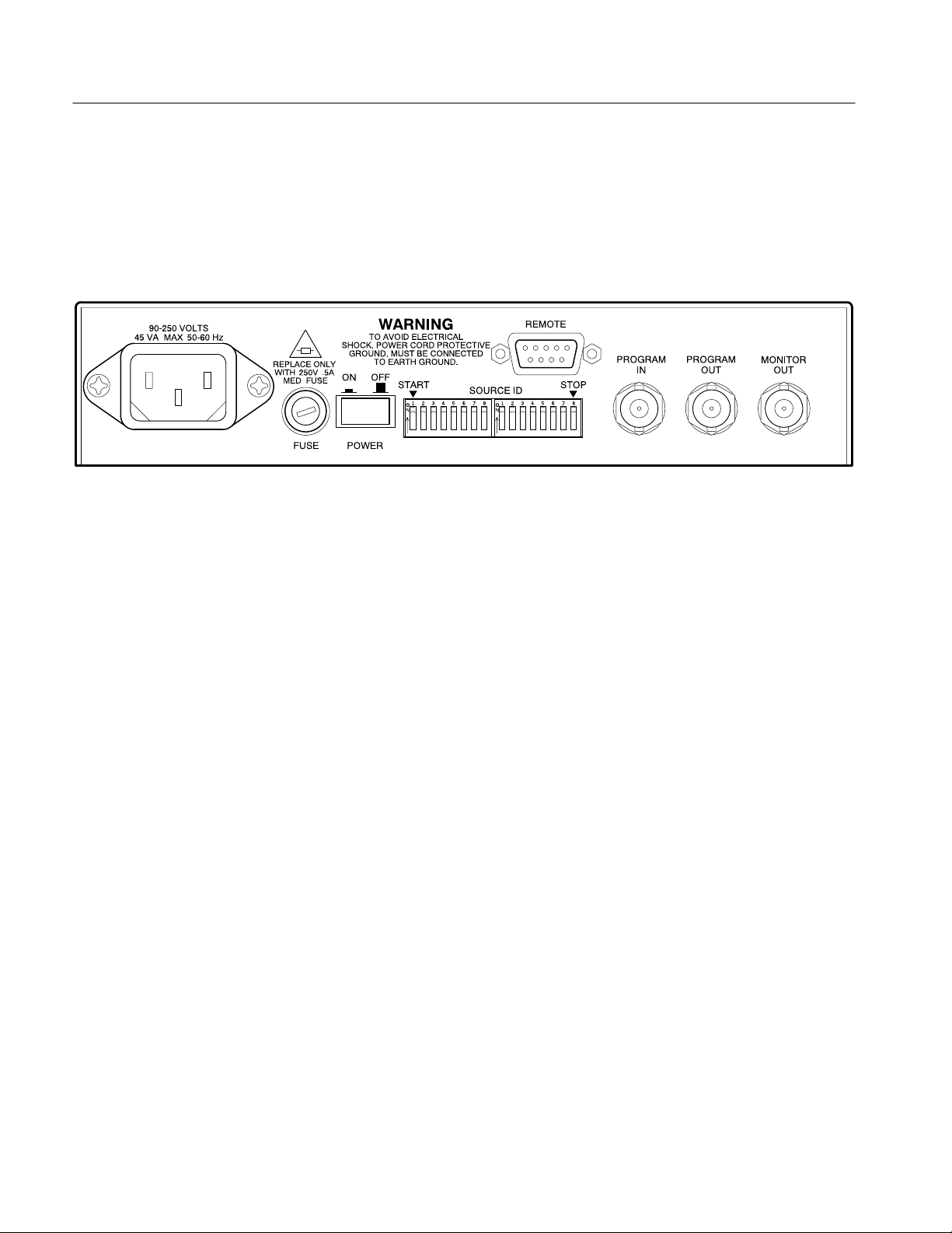
Rear Panel
The VITS100 NTSC VITS Inserter rear panel, shown in Figure 2–2, contains the
mains power input, switch, and fuse; the program input and output connectors;
DIP switches for source identification code selection; and a remote connector.
Figure 2–2: VITS100 NTSC VITS Inserter rear panel
Power
Source ID
The power block consists of the connector, fuse, and power switch. It is located
on the left third of the panel.
Power Connector. This instrument uses a power supply that accepts line voltages
from 90 to 250 VAC without changing voltage ranges or fuses.
Fuse. The fuse holder accepts a standard cartridge fuse. See the rear panel or the
Replaceable Electrical Parts section of this manual for the correct value.
Switch. A push-push, on-off switch; power is on when the switch is latched in the
in position, as indicated by the rear-panel graphic.
This set of two dual in-line package (DIP) switches is used to select a source
identification code. The source ID is a one-line, 16-bit word consisting of a start
and stop bit and any one of 16,384 (2
can be inserted in the vertical interval (lines 17 through 20) to identify the source
of the program signal.
The source ID signal is accepted by other video equipment, such as the Tektronix
VM 700A Video Measurement Set, which can then include the source ID in
reports or printouts to identify the source of the signal being measured.
14
) possible identification codes. The ID
2–2
Program In
The PROGRAM IN connector is the program video input. The input is AC
coupled, clamped to ground, and internally terminated in 75 W.
VITS100 NTSC VITS Inserter Instruction Manual
Page 29

Operating Basics
Program Out
Monitor Out
Remote Connector
Insertion Options
The PROGRAM OUT connector is the program video output. Output video can
have user-selected VITS inserted on selected lines. If the instrument cannot lock
to the program input video signal, or if power fails, the program automatically
bypasses the VITS inserter processing circuitry; the input signal is then routed
through a delay line, with a delay equivalent to the processing delays of the
instrument, to PROGRAM OUT. Matching the delay eliminates timing errors
whenever the VITS inserter must enter bypass mode.
This connector provides the same output as the PROGRAM OUT connector,
except that the MONITOR OUT is not in the bypass signal path. This means
that —during loss of genlock or activation of the bypass mode—the monitor
output will still contain any inserted VITS. There is no output from this
connector if power is lost.
This 9-pin connector enables ground-closure remote control of bypass mode. In
addition, control lines that parallel the three front panel indicators (POWER,
BYPASS, and UNLOCKED) are brought out to this connector.
Inserting Test Signals
You can configure the VITS inserter to insert test signals, pass existing video,
insert or pass VIRS, or insert a source ID on lines 17, 18, 19, and 20 of both the
even and odd fields of NTSC video.
The standard VITS100 NTSC VITS Inserter can insert the following test signals
into the vertical interval:
H FCC Color Bars H FCC Composite
H FCC Multiburst H NTC7 Combination
H NTC7 Composite H VIRS
H 7.5% Black H 0% Black
H Multipulse H SIN X/X
H Red Field H 50% Gray
You can find descriptions of these waveforms in the Specifications section of this
manual. If your instrument contains Option 1J, Option 1M, or Option 2, see
Appendix A: Options for descriptions of the optional signals.
VITS100 NTSC VITS Inserter Instruction Manual
2–3
Page 30
Operating Basics
Passing Program Video
Auto VIRS
Inserting a Source ID
In addition to internally generated test signals, the VITS inserter can pass video
signals that are already in the vertical interval of the program video. This
includes the delete/insert lines, which are lines 17 through 20 in all fields.
When AUTO VIRS is selected, the instrument automatically checks the assigned
line and field of the incoming video for a VIRS signal. If VIRS is detected, the
line is passed with no processing. If VIRS is not detected, the internally
generated VIRS signal is inserted onto the line.
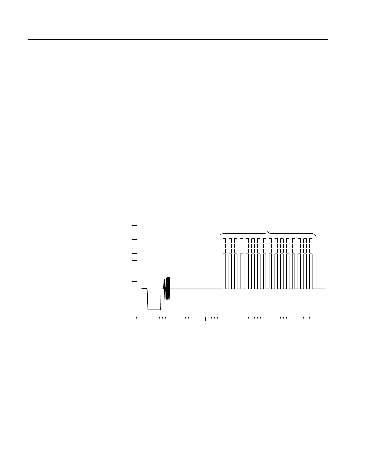
Source identification can be inserted on any of the available vertical interval
lines. The “Source ID” consists of sixteen equal-duration flags that can be set
high or low with the rear-panel SOURCE ID switches. Source ID is set by the
user to provide a visual identification of the signal path. Some equipment, such
as the Tektronix VM700A Video Measurement Set, can use this signal to
generate an alpha-numeric ID on the screen display or on printed reports. Figure
2–3 shows the waveform of a source identification code that is generated when
all switch segments are set ON.
Source Identification
Switches all on
(S/N 8020244 and below)
0.5
Volts
0.0
(S/N 8020245 and up)
0.0
10.0 20.0 30.0 40.0 50.0 60.0
MicroSeconds
Figure 2–3: VITS100 NTSC VITS Inserter source ID signal
2–4
VITS100 NTSC VITS Inserter Instruction Manual
Page 31

Operating Basics
Factory Configuration
The VITS100 NTSC VITS Inserter is configured during manufacture to insert
the signals listed in Table 2–1. See VITS Selection, below, for instructions on
configuring the VITS inserter to insert the signals that best suit your applications
and facility.
T able 2–1: Standard Factory-Programmed Signals
Field Line Signal
1 17 NTC7 Composite signal
1 18 Pass*
1 19 VIRS
1 20 Pass*
2 17 NTC7 Combination signal
2 18 Pass*
2 19 VIRS
2 20 Pass*
* Passed lines are not deleted or inserted by the VITS 100 NTSC VITS Inserter
VITS Selection
VITS signal selection for the individual vertical interval lines is made with four
DIP switches (S1–S4) mounted on the VITS inserter circuit board. Remove the
small panel from the top cover of the VITS inserter, as shown in Figure 2–4, to
gain access to these switches.
VITS100 NTSC VITS Inserter Instruction Manual
2–5
Page 32

Operating Basics
Screws (2)
Cover
Switch/Line Assignments
Figure 2–4: Location of VITS selection switches
Switches S1 and S2 make the selections for fields 1 and 3, and switches S3 and
S4 make the selections for fields 2 and 4. Each DIP switch selects the test signals
for two of the vertical interval lines, as shown in Figure 2–5.
Program color fields
1 and 3
Line 18Line 17
Line 20Line 19
S1 S2 S3 S4
Program color fields
2 and 4
Line 18Line 17
Line 20Line 19
2–6
Figure 2–5: The VITS selection DIP switches
VITS100 NTSC VITS Inserter Instruction Manual
Page 33

Operating Basics
Switch Settings
The switch settings for signal selection are listed in Table 2–2. When a switch
segment is thrown to the left (as viewed from the front of the VITS inserter), it is
open; when thrown to the right, it is closed. Open positions are denoted in the
table as 1, and closed are denoted as 0.
T able 2–2: DIP Switch Settings
VITS inserter Action DIP Segment Settings*
1 (5) 2 (6) 3 (7) 4 (8)
Insert Test Signal:
0% Black (two settings)
7.5% Black 1 1 1 0
50% Gray 1 1 0 1
FCC Color Bars 0 0 0 0
FCC Composite 1 0 0 0
Multiburst 0 1 0 1
Multipulse 0 1 0 0
NTC 7 Composite 1 0 1 0
NTC 7 Combination 0 0 0 1
0 1 1 0
1 0 0 1
Red Field 1 1 0 0
SIN X/X 0 0 1 0
VIRS 1 0 1 1
Pass Program Video 1 1 1 1
Auto VIRS 0 0 1 1
Insert Source ID 0 1 1 1
* 1 signifies an OPEN switch; 0 signifies a closed switch
VITS100 NTSC VITS Inserter Instruction Manual
2–7
Page 34

Operating Basics
Remote Control
Remote control in the standard VITS100 NTSC VITS Inserter is limited to
ground-closure Bypass control and (+5 V) outputs for remote BYPASS,
UNLOCKED, and POWER indicator lights. See Figure 2–6 and Table 2–3 for
the rear-panel REMOTE connector pin assignments.
REMOTE
51
96
VITS Inserter
Figure 2–6: The REMOTE connector
T able 2–3: REMOTE Connector Pin Assignments
Function Pins
Ground 1, 5
Force Bypass 6
BYP ASS Indicator 2
UNLOCKED Indicator 7
POWER Indicator 3
To duplicate the function of the front panel at a remote location, run a cable from
REMOTE pins 1, 2, 3, 5, 6, and 7 to an SPST switch and three indicator LEDs.
H Connect the switch between pins 1 and 6.
H Connect the Bypass indicator between pins 2 and 5.
H Connect the Unlocked indicator between pins 7 and 5.
H Connect the Power indicator between pins 3 and 5.
2–8
Close the switch to force the VITS inserter into bypass mode; the LEDs light
with the corresponding front-panel indicators.
VITS100 NTSC VITS Inserter Instruction Manual
Page 35

Specifications
Page 36

Page 37

Specifications
This section contains tables that list the specifications for the VITS100 NTSC
VITS Inserter. All specifications are guaranteed unless noted “typical.”
The performance limits in this specification are valid with these conditions:
H The VITS inserter must have been calibrated/adjusted at an ambient
temperature between +20
H The VITS inserter must be in an environment with temperature, altitude,
humidity, and vibration within the operating limits described in these
specifications.
H The VITS inserter must have had a warm-up period of at least 20 minutes.
Specification Tables
T able 3–1: Program channel characteristics
Characteristic Information
_ C and +30_ C.
Gain Unity ± 1%
Frequency Response ±1% to 5.5 MHz
±3% to 10 MHz
Chrominance-to-Luminance Gain ±0.5%
Chrominance-to-Luminance Delay ≤5 ns
Diff Phase ≤0.2°
Diff Gain ≤0.2%
Line Tilt ≤0.5%
DC Output Level 0 V ±10 mV
DC Matching of Inserted Test Signal to
Program Signal
Phase Match (Relay Bypass Path to Signal
Processing Path)
Hum Rejection 50 dB (Measured right after burst)
Keyboard (No Noise) Too small to measure on VM700A
Insertion Transients ≤10 mV (Measured on Tektronix 1780R. Typically <5 mV)
Input Impedance 75 W
Return Loss 36 dB to 5 MHz (Program In, Program Out, and Monitor Out)
±3 mV
±1° at F
SC
VITS100 NTSC VITS Inserter Instruction Manual
3–1
Page 38

Specifications
T able 3–1: Program channel characteristics (Cont.)
Characteristic Information
Phase Matching of Inserted Test Signal to
Program Video
Pulse to Bar Ratio 100%±0.5% (Typically within ±0.25%)
Signal to Noise Ratio >70 dB (Unweighted Filter at 5 MHz. Measured 91 dB on VM700A, relative to reference)
±1° (Program Sync and Burst Normal Level)
T able 3–2: Test Signal and Black Burst general characteristics
Characteristic Information
Frequency Response ±1% to 5 MHz
±5% to 10 MHz
Luminance Amplitude Accuracy ±1%
Chrominance-to-Luminance Gain ±0.5%
Chrominance-to-Luminance Delay ≤5 ns
Diff Phase ≤0.3°
Diff Gain ≤0.3%
Line Tilt ±0.5%
Output Impedance 75 W
Signal to Noise Ratio >78 dB (Measured on a VM700A with an unweighted 5 MHz lowpass filter.)
Spurious Signals (5 MHz 50 MHz)
Pulse to Bar Ratio 100% ±0.5%
K Factor (K2T) 0.3% (Typically 0.2%)
Crosstalk ≥60 dB down
DC Offset 0 V DC ±10 mV
SCH Phase Accuracy 0 ±5° (< ±2.5° typical)
Luminance Rise Time 140 ns ±20 ns
Chrominance Rise Time 300 ns ±35 ns
>55 dB down
T able 3–3: Black and Gray Test Signal characteristics
Signal Information
0% Black 0 IRE Luminance with sync and burst; see Figure 3–1.
7.5% Black 7.5 IRE Luminance with sync and burst; see Figure 3–2.
50% Gray 50 IRE Luminance with sync and burst; see Figure 3–3.
3–2
VITS100 NTSC VITS Inserter Instruction Manual
Page 39

T able 3–4: FCC Composite characteristics
Characteristic Information
Timing See Figure 3–5
Modulated 5-step Staircase
Luminance
Amplitude 80.4 IRE ±0.7 IRE
Riser Amplitude 1/5 of 5-step amplitude ±0.5%
Rise Time 250 ns ±25 ns
Chrominance
Phase Same as burst ±0.3°
Envelope Risetime 375 ns ±37.5 ns
2T Pulse
Pulse-to-Bar Ratio 100% ±0.5%
Half Amplitude Duration (HAD) 250 ns ±25 ns
Ringing 1.0 IRE or less
Modulated SIN2 Pulse
Pulse-to-Bar Peak Amplitude 100%
Half Amplitude Duration 1.563 ms ±150 ns
Phase 60.8° ±1°
Bar
Amplitude 100 IRE ±1 IRE
Rise Time 250 ns ±25 ns
Specifications
VITS100 NTSC VITS Inserter Instruction Manual
3–3
Page 40

Specifications
T able 3–5: FCC Color Bars characteristics
Characteristic Information
Timing See Figure 3–4
Luminance Rise Time 250 ns ±25 ns
Bar Characteristics: White Yellow Cyan Green Magenta Red Blue Black
Luminance Amplitude (mV p-p)
Subcarrier Amplitude (mV p-p)
Subcarrier Phase (degrees)
714.3
0.0
0.0
494.3
444.2
167.1
400.7
630.1
283.4
345.7
588.5
240.8
256.0
588.5
60.8
202.1
630.1
103.4
107.8
444.2
347.1
T able 3–6: Multiburst characteristics
Characteristic Information
Timing See Figure 3–6
White Reference Bar Amplitude 100 IRE
Packet Amplitudes 60 IRE p-p
Pedestal 40 IRE
Burst Frequencies 500 kHz, 1.25 MHz, 2.0 MHz, 3.0MHz, 3.58 MHz, 4.1 MHz
Packet Rise Time
500 kHz 140 ns typical (sin2 shaped packets)
Other Packets 400 ns typical (sin2 shaped packets)
53.5
0.0
0.0
T able 3–7: Multipulse characteristics
Characteristic Information
Timing See Figure 3–7
Amplitudes 80 IRE
Frequencies 1.0 MHz, 2.0 MHz, 3.0 MHz, 3.58 MHz, and 4.2 MHz
3–4
VITS100 NTSC VITS Inserter Instruction Manual
Page 41

T able 3–8: NTC7 Combination characteristics
Characteristic Information
Timing See Figure 3–8
White Reference Bar
Amplitude 100 IRE ±0.7 IRE
Rise Time 250 ns ±25 ns
Multiburst Packets
Amplitude 50 IRE ±0.5 IRE p-p
Average Level 50 IRE ±0.5 IRE
Frequencies 500 kHz, 1.0 MHz, 2.0 MHz, 3.0 MHz, 3.58 MHz, 4.2 MHz
Packet Rise Time
500 kHz and 1.0 MHz 140 ns typical (sin2 shaped packets)
Other Frequencies 400 ns typical (sin2 shaped packets)
Modulated Pedestal
Pedestal
Amplitude 50 IRE ±0.5 IRE
Rise Time 250 ns ±25 ns
Chrominance
Amplitude
20 IRE 20.01 IRE ±0.5 IRE
40 IRE 40.02 IRE ±0.5 IRE
80 IRE 80.04 IRE± .5 IRE
Phase relative to burst 90° ±0.5°
Rise Time 400 ns ±40 ns
Specifications
VITS100 NTSC VITS Inserter Instruction Manual
3–5
Page 42

Specifications
T able 3–9: NTC7 Composite characteristics
Characteristic Information
Timing See Figure 3–9
Modulated 5-step Staircase
Luminance
Amplitude 90.2 IRE ±0.7 IRE
Riser Amplitude 1/5 of 5-step amplitude ±0.5%
Rise Time 250 ns ±25 ns
Chrominance
Phase Same as burst ±0.3°
Envelope Risetime 400 ns ±40 ns
2T Pulse
Pulse-to-Bar Ratio 100% ±0.5%
Half Amplitude Duration (HAD) 250 ns ±25 ns
Ringing 1.0 IRE or less
Modulated SIN2 Pulse
Pulse-to-Bar Peak Amplitude 100%
Half Amplitude Duration 1.563 ms ±150 ns
Phase 60.8° ±1°
Bar
Amplitude 100 IRE ±1 IRE
Rise Time 125 ns ±15 ns
T able 3–10: Red Field characteristics
Characteristic Information
Timing See Figure 3–10
Luminance
Amplitude, Standard 202.2 mV ±1%
Amplitude, Option 1J 160.72 mV ±1%
Rise Time 250 ns ±25 ns
Chrominance
Amplitude, Standard 630.1 mV ±1%
Amplitude, Option 1J 681.23 mV ±1%
Phase 103.4° ±0.3°
Rise Time 400 ns ±40 ns
3–6
VITS100 NTSC VITS Inserter Instruction Manual
Page 43

T able 3–11: SIN X/X characteristics
Characteristic Information
Timing See Figure 3–1 1
Bandwidth 4.75 MHz
Pedestal 24 IRE
Peak 90 IRE (Peak amplitude from pedestal )
T able 3–12: Vertical Interval Reference Signal characteristics
Characteristic Information
Timing See Figure 3–12
Chrominance Reference
Amplitude 40 IRE
Phase Same as burst ±0.3°
Envelope Rise Time 1 ms ±100 ns (sin2 shaped)
Average Chrominance Level 70 IRE
Luminance Reference
50 IRE Level 50 IRE
Black Reference 7.5 IRE
Specifications
T able 3–13: Cable Multiburst (Option 2) characteristics
Characteristic Information
Timing See Figure 3–13
White Reference Bar Amplitude 60 IRE
Packet Amplitudes 60 IRE
Pedestal Amplitudes 30 IRE
Burst Frequencies 500 kHz, 1.25 MHz, 2.0 MHz, 3.0 MHz, 3.75 MHz, 4.0 MHz
Packet Rise Time
500 kHz Packet 140 ns typical (sin2 shaped packets)
Other Packets 400 ns typical (sin2 shaped packets)
VITS100 NTSC VITS Inserter Instruction Manual
3–7
Page 44

Specifications
T able 3–14: Cable Sweep (Option 2) characteristics
Characteristic Information
Timing See Figure 3–14
Pedestal Amplitude 50 IRE
Sweep Amplitude 100 IRE
Sweep Start Frequency 0.1 MHz
Sweep End Frequency 4.2 MHz
T able 3–15: Genlock characteristics
Characteristic Information
Burst Lock
Genlock Phase Change with Input
Amplitude
Genlock Phase Change with Input
Signal APL
Genlock Phase Change with Input
Signal Burst Frequency
Lock Range
Frequency , Standard 3.579545 MHz ±20 Hz (NTSC)
Fequency, Option 1M 3.575611 MHz ±20 Hz (PAL-M)
Amplitude +6 dB to –12 dB (Typically to –16 dB NTSC; –14 dB PAL-M)
Genlock Phase Jitter with Input Amplitude
Change
≤2° burst phase change for input sync or burst amplitude range of 287mV ±3 dB
≤4° burst phase change for amplitude range of 287mV ±6dB
(For either composite video or burst amplitude errors)
≤1° burst phase change over 10% to 90% APL
≤1° burst phase change for ±20 Hz change in incoming subcarrier
Typically ≤0.2° peak for input sync or burst amplitude range of 287 mV ±3dB; no noise
on input signal
Typically ≤0.4° peak for input amplitude range of 287 mV ±6 dB; no noise on input signal
Sync Lock Jitter ≤10 ns for input sync amplitude range of 287 mV ±3 dB (No noise on input signal)
Noise Performance Locks to 28 dB S/N Ratio Video
3–8
VITS100 NTSC VITS Inserter Instruction Manual
Page 45

Specifications
T able 3–16: Power Supply characteristics
Characteristic Information
Output Voltages +5 V ±200 mV from 1A to 3 A (voltage adjustable)
–5.2 V ±300 mV from 0.5 A to 1 A
±12 V ±120 mV from 0.05 A to 0.2 A (post regulated from ±14.5 V by linear regulators)
Output Ripple
+5 V ≤50 mV switching ripple,
≤5 mV line frequency ripple
–5.2 V ≤50 mV switching ripple,
≤10 mV line frequency ripple
±12 V ≤10 mV switching ripple,
≤5 mV line frequency ripple
Line Input Range Regulates from 90 to 250 VAC
Minimum Load 10 W minimum load required to operate. However, output voltages other than +5 V may
not meet specifications outside the listed currents. At zero load the power supply cycles
on and off
Power Consumption 40–50 W.
Overvoltage Protection The 5 V output is protected by a crowbar circuit that engages at approximately 5.7 V.
Overvoltage protection causes the power supply to cycle by engaging the primary side
current limit time-out circuit
Power 70 W maximum controlled by primary side current limit circuits. Power supply cycles on
and off when power limit is reached
Short-Circuit Protection All outputs are protected by the primary side current limit and time-out circuits. In
addition, the ±12 V outputs are limited to 1 A by the linear regulators
Efficiency 70% nominal
Fan Drive 15 V to 16.5 V , as determined by supply load
T able 3–17: Physical characteristics
Characteristic Information
Height 1.734 in (4.404 cm)
Width 8.1 in (20.6 cm)
Length 17.2 in (43.7 cm)
Weight
Net 4.7 lbs (2.1 kg)
Shipping 16.7 lbs (7.6 kg)
VITS100 NTSC VITS Inserter Instruction Manual
3–9
Page 46

Specifications
T able 3–18: Environmental characteristics
Characteristic Information
Temperature
Non-Operating –40° to +65° C (–40° to +149° F)
Operating 0° to +50° C (32° to 122° F)
Altitude
Non-Operating To 50,000 ft (15,240 m)
Operating To 15,000 ft (4,572 m)
Vibration (Operating) Fifteen minutes each axis at 0.025 inch, frequency varied from 10-55-10 Hz in 4-minute
cycles with the instrument secured to the vibration platform; ten minutes each axis at any
resonant point, or at 55 Hz.
Shock 50 G, 1/2 sine, 11 ms duration, three guillotine shocks per side
Transportation Qualified under NTSB Test Procedure 1A, Category II (36-inch drop)
3–10
VITS100 NTSC VITS Inserter Instruction Manual
Page 47

T able 3–19: Certifications and compliances
Category Standards or description
Specifications
EC Declaration of Conformity –
EMC
Australia/New Zealand
Declaration of Conformity – EMC
EMC Compliance Meets the intent of Directive 89/336/EEC for Electromagnetic Compatibility when it is used with the
FCC Compliance Emissions comply with FCC Code of Federal Regulations 47, Part 15, Subpart B, Class A Limits.
Installation (Overvoltage)
Category
Pollution Degree A measure of the contaminates that could occur in the environment around and within a product.
Safety Standards
U.S. Nationally Recognized
Testing Laboratory Listing
Canadian Certification CAN/CSA C22.2 No. 231 CSA safety requirements for electrical and electronic measuring and
European Union Compliance Low V oltage Directive 73/23/EEC, amended by 93/69/EEC
Meets intent of Directive 89/336/EEC for Electromagnetic Compatibility. Compliance was
demonstrated to the following specifications as listed in the Official Journal of the European Union:
EN 50081-1 Emissions:
EN 55022 Class B Radiated and Conducted Emissions
EN 50082-1 Immunity:
IEC 801-2 Electrostatic Discharge Immunity
IEC 801-3 RF Electromagnetic Field Immunity
IEC 801-4 Electrical Fast Transient/Burst Immunity
Complies with EMC provision of Radiocommunications Act per the following standard(s):
AS/NZS 2064.1/2 Industrial, Scientific, and Medical Equipment: 1992
AS/NZS 3548 Information Technology Equipment: 1995
product(s) stated in the specifications table. Refer to the EMC specification published for the stated
products. May not meet the intent of the directive if used with other products.
Terminals on this product may have different installation (overvoltage) category designations. The
installation categories are:
CA T III Distribution-level mains (usually permanently connected). Equipment at this level is
typically in a fixed industrial location.
CA T II Local-level mains (wall sockets). Equipment at this level includes appliances, portable
tools, and similar products. Equipment is usually cord-connected.
CA T I Secondary (signal level) or battery operated circuits of electronic equipment.
Typically the internal environment inside a product is considered to be the same as the external.
Products should be used only in the environment for which they are rated.
Pollution Degree 2 Normally only dry , nonconductive pollution occurs. Occasionally a
temporary conductivity that is caused by condensation must be
expected. This location is a typical office/home environment.
Temporary condensation occurs only when the product is out of
service.
UL1244 Standard for electrical and electronic measuring and test equipment.
test equipment.
EN 61010-1 Safety requirements for electrical equipment for measurement,
VITS100 NTSC VITS Inserter Instruction Manual
control, and laboratory use.
3–11
Page 48

Specifications
T able 3–19: Certifications and compliances (Cont.)
Category Standards or description
Additional Compliance IEC61010-1 Safety requirements for electrical equipment for measurement,
control, and laboratory use.
Safety Certification Compliance
T emperature, operating +5 to +40_ C
Altitude (maximum
operating)
Equipment Type Test and measuring
Safety Class Class 1 (as defined in IEC 1010-1, Annex H) – grounded product
Overvoltage Category Overvoltage Category II (as defined in IEC 1010-1, Annex J)
Pollution Degree Pollution Degree 2 (as defined in IEC 1010-1). Note: Rated for indoor use only.
2000 meters
Waveform Diagrams
The diagrams in Figures 3–1 through 3–14 contain timing information for the
various test signals generated by the VITS100 NTSC VITS Inserter and
described in Tables 3–3 through 3–14.
Figure 3–1: 0% Black
3–12
VITS100 NTSC VITS Inserter Instruction Manual
Page 49

Figure 3–2: 7.5% Black
Specifications
Figure 3–3: 50% Gray
VITS100 NTSC VITS Inserter Instruction Manual
3–13
Page 50

Specifications
Figure 3–4: FCC Color Bars
3–14
Figure 3–5: FCC Composite
VITS100 NTSC VITS Inserter Instruction Manual
Page 51

Figure 3–6: Multiburst
Specifications
Figure 3–7: Multipulse
VITS100 NTSC VITS Inserter Instruction Manual
3–15
Page 52

Specifications
Figure 3–8: NTC7 Combination
3–16
Figure 3–9: NTC7 Composite
VITS100 NTSC VITS Inserter Instruction Manual
Page 53

Figure 3–10: Red Field
Specifications
Figure 3–11: SIN X/X
VITS100 NTSC VITS Inserter Instruction Manual
3–17
Page 54

Specifications
Figure 3–12: VIRS
3–18
Figure 3–13: Cable Multiburst
VITS100 NTSC VITS Inserter Instruction Manual
Page 55

Figure 3–14: Cable Sweep
Specifications
VITS100 NTSC VITS Inserter Instruction Manual
3–19
Page 56

Specifications
3–20
VITS100 NTSC VITS Inserter Instruction Manual
Page 57

WARNING
The following servicing instructions are for use only by qualified personnel. To
avoid injury, do not perform any servicing other than that stated in the operating
instructions unless you are qualified to do so. Refer to all Safety Summaries before
performing any service.
Page 58

Page 59

Theory of Operation
Page 60

Page 61

Theory of Operation
This section of the manual begins with a functional description of the circuitry.
This brief discussion is followed by a more detailed set of circuit descriptions
that take you to the individual component level of the schematic diagrams.
Functional Description
Program In. The program input is buffered and clamped. The clamped program
video drives the Sync Stripper that strips off composite sync and generates the
backporch timing for the Clamp.
Genlock. The genlock calculates the SCH phase of the incoming video to
determine the correct color framing. A phase-locked loop is used to control a
voltage-controlled oscillator (VCO). When the VITS inserter is genlocked, a
frame reset pulse is generated to align the test signal counters with genlock
counters.
T est Signal Generation. The VITS100 NTSC VITS Inserter can insert four lines
on odd and even fields. Signals are selected with four DIP switches on the main
circuit board. The lines from the switches are multiplexed and form one of the
inputs to the Test Signal Generator.
Test signals are generated by clocking data from PROMs to a digital-to-analog
converter (DAC) at an 8
before driving the VITS Inserter.
Program Out. The VITS inserter video signal output can be from any of three
sources: clamped video through the instrument, VITS signals inserted on one of
the four VITS lines, or the bypassed program line. The bypassed program line
has a built-in delay line to maintain the precise time relationship between the
processed and bypassed video.
Remote Control. Remote control is limited to ground-closure bypass control and
the power, unlocked, and bypass indicator lines.
Power Supply . The power supply, located on the Inserter board, is a current-mode
controlled, discontinuous, flyback, switching power supply. The current output is
distributed among the four supplies.
rate. The output of this DAC is filtered and buffered
FSC
VITS100 NTSC VITS Inserter Instruction Manual
4–1
Page 62

Theory of Operation
Circuit Description
The power inductor is driven by switching the voltage to its primary winding on
and off at a rate of approximately 45 kHz. The power inductor is used as an
energy storage device. Energy is stored in the primary during the first half of the
switching cycle. On the second half of the switching cycle, the stored energy is
transferred to the secondaries.
Regulation is accomplished through feedback from the +5 V supply to the Pulse
Width Modulator that controls the primary voltage. The Pulse Width Modulator
varies the length of time that voltage is applied to the primary changing the
amount of stored energy.
All primary voltages are referenced to a floating ground, not chassis ground. An
isolation transformer or a differential amplifier is therefore required for troubleshooting the circuitry in the primary and the Pulse Width Modulator.
The following circuit description takes you down to the component level.
Because of the arrangement of circuits on the schematic diagrams, most of the
functional headings cover circuits that appear on more than one schematic
diagram.
Test Signal Generation
In this discussion active-low signals are denoted by overbars (like this
names are in lower case and enclosed in quotation marks (“like this”).
The circuitry that generates the test signals for insertion appears on three of the
schematic diagrams located in the Diagrams section of this manual. Key
circuitry is located on diagrams 1 (Test Signal Memory), 3 (H & V Counters,
Source Identification & Bypass Controls), and 7 (Analog Output).
Diagram 3. Test signal generation starts with a 4
Horizontal Counter, U28, to provide 910 counts per line of video. In addition,
this counter decodes the backporch clamp pulse, for the test signal. The output of
the Horizontal Counter drives a Horizontal Decoder PROM, U27, to provide
timing signals for various functions. The Horizontal Counter is reset by the
frame pulse, from the genlock circuitry in order to time the test signals to
program video.
A once-per-line pulse from the Horizontal Decoder PROM (pin 14) enables the
Vertical Counter, U24. This synchronous output of the Vertical Counter drives
the Vertical Decoder PROM, U25. Output of U25 is latched twice per line by
U26, which is clocked by the “vlatch” from U27 (pin 16).
clock that clocks the
FSC
). Signal
4–2
Diagram 1. Test signal data is stored in PROMs U4, U5, and U6. U4 and U5 store
the eight MSBs of alternate data samples. U6 stores the four LSBs for all data
VITS100 NTSC VITS Inserter Instruction Manual
Page 63

Theory of Operation
samples. The outputs of U4 and U5 are multiplexed by U82 and U83 to increase
the data rate from 4
FSC
to 8
. The outputs of U82 and U83 are latched by U1
FSC
before being converted to ECL levels. U9 and U10 are the level converters for
the DAC, U65, which is located on Diagram 7. The four LSBs are latched by U3
and then selected by a multiplexer, U7 before being converted to ECL levels by
U11.
Test signal data is stored in U4, U5, and U6 in blocks of eight. The blocks of
data are addressed by the Block PROM, U13, and two test signal select lines.
When the test signal select circuitry calls for a given test signal, the Block
PROM uses V1 to determine the correct phase of subcarrier, uses “halfline” to
determine when to generate a half line, and uses the seven MSBs of horizontal
count to select the appropriate blocks of data.
Diagram 7. The U65 is a 12-bit DAC that turns the data into analog voltage levels
at an 8
rate. A one-volt reference is generated for the DAC by U84. The
FSC
analog output signal is filtered by a 7-pole filter, L12, L13, and L14, with T2
functioning as a second order group delay correction.
Genlock
The signal is AC coupled to a buffer, U67, and clamped to remove any DC level
change with temperature. This allows the test signal DC level to match the
Program Video DC level very accurately.
This video buffer drives the Channel Switch, U64, which switches between
Program Video and VITS. The output of Channel Switch drives the MONITOR
OUT and the Program Output.
K2 controls the signal to the PROGRAM OUT. It switches the PROGRAM IN
through a delay line, L7, L3, and C52 to the PROGRAM OUT when the power
shuts off or when the front-panel RELAY BYPASS button is pushed. The delay
line in this bypass mode matches the time it takes for the video to travel through
the processing circuitry.
The circuitry that genlocks to the incoming program signal appears on three of
the schematic diagrams in the Diagrams section of this manual. Key circuitry is
located on diagrams 4 (Genlock), 5 (Program Input, Sync Stripper, VIRS
Detection, & Genlock A/D Input), and 6 (Clocks).
Diagram 5. U42 buffers and clamps the program input signal The output of U42
also drives the Sync Stripper, U44. U44 strips off the composite sync and
generates the backporch timing pulse used by the clamps.
Composite sync and the backporch timing are shifted to TTL levels by Q1, Q3,
VR1, and VR2. Their outputs are gated together by U57A and U57B to produce
the clamp pulse for U42.
VITS100 NTSC VITS Inserter Instruction Manual
4–3
Page 64

Theory of Operation
The Input Buffer, U42, also drives the genlock analog-to-digital converter
(ADC), U43. The ADC also has AGC and is clamped with “synctip” and
“backporch” signals, which provide the timing.
The clamped and AGC’d video is then routed through an anti-aliasing filter (L1,
C19, C20, and C21), and then reinput to the ADC where it is digitized. The
digital output is input to a PAL, U41. where it is inverted and latched. The signal
“sis_tm” from the genlock ASIC, on diagram 4, holds the same sample across
the bottom of sync to block Sound-in-Sync pulses from upsetting the genlock
circuitry.
Diagram 4. The output data from the PAL on diagram 3 is input to the Genlock
ASIC, U29, which has RAM, counters, decoders, and the other genlocking
circuitry. Composite sync is routed to the genlock ASIC through a PAL, U70.
The genlock ASIC uses the composite sync to roughly position the horizontal
and vertical counters.
The Genlock Processor, U35, is an 8 MHz Z80 that calculates the SCH of the
incoming video in order to determine the correct color framing. The processor
uses the digitized color subcarrier burst to determine the tangent of the phase
angle between the system clock and the burst. This tangent is used to look up the
arctangent (that is, the angle itself), which is stored in a PROM, U33. The angle
is used as a correction to the system clock, on diagram 6, to form a phase-locked
loop.
Diagram 6. The correction is an 8-bit word which is sent to DAC, U59. The
output of the DAC is integrated by an operational amplifier, U61A and C46. U60
is an analog switch that is used to short the integrator when searching for
genlock and to change the loop characteristics once lock is securely acquired.
The processor also increases loop gain once lock has been acquired and enables
the Genlock ASIC to output a frame reset pulse to align the test signal counters
with the genlock counters.
Y39 is the clock for the genlock processor (NOT the system clock). U31 is a
hardware watchdog that resets the processor if it fails to receive an “awake”
signal from the processor within the right amount of time. U38 latches control
signals “glk/int
” and “acq/hold” for U60, an analog switch, and the signal
“locked” to signify that genlock has been achieved. Counter/Timer U30 is used
to distinguish between even and odd fields of video.
Genlock sub-clock cycle timing can be adjusted up to 90
d
with S7. The VITS
signals are timed to program video input at the factory and should not need
adjustment.
S8 is a diagnostics switch; see the Maintenance section for details.
4–4
VITS100 NTSC VITS Inserter Instruction Manual
Page 65

Theory of Operation
Signal and Switching
Control
The circuitry that controls signal switching appears on three of the schematic
diagrams in the Diagrams section of this manual. Key circuitry is located on
diagrams 1 (Test Signal Memory), 2 (Test Signal Select), and 5 (Program Input,
Sync Stripper, VIRS Detection, & Genlock A/D Input).
Diagram 2. Signal selection is accomplished with four dual in-line package (DIP)
switches, S1, S2, S3, and S4. The lines from the switches are multiplexed by
U18, U19, U20, and U21
to select the appropriate switch segments at the correct time (S1 segments 1
through 4 during line 17 odd fields, for example).
The multiplexing is controlled by two bits from the Vertical Decoder and the
field signal from the Vertical Counters on diagram 3. Two PALs, U16 and U17,
located on diagram 1, decode control signals and latch the signal selections. U16
latches the bits to the test signal PROMs, and decodes when the source ID signal
is requested. Signals “vdrive” and “vsync” force the generation of vertical sync.
Diagram 5. U17, on diagram 1, decodes when Auto VIRS has been requested. It
enables the circuitry that compares program video to the VIRS test signal to
determine if VIRS is present on program video. U46 is an operational amplifier
that subtracts low-pass filtered program video from filtered test signals and
drives U47A and U47B, a window comparator.
Source ID Generation
If the program signal and the test signal match closely enough, the comparator
output remains high and the output of an OR gate, U48A, remains high; a one
shot, U71B, is not triggered. The OR gate can only trigger the one shot when
U17, on diagram 1, determines that Auto VIRS has been requested and drives
“virsamp
and “ccvirs” from U17 is sent to U14 to control insertion.
Diagram 1. U17 also decodes “dvdrive” and “dvsync” which are delayed from
“vdrive” and “vsync” by a half line and therefore are timed with the actual test
signals that are generated.
U14 takes the information from U16 and U17, “chswt” (the insertion timing
signal), and other timing signals; it then determines two control signals for the
program channel switch, “sw0” and “sw1,” and one signal to choose between
source ID generation and test signal generation, “ts/char
The circuitry that controls source ID generation appears on two of the schematic
diagrams in the Diagrams section of this manual. Key circuitry is located on
diagrams 1 (Test Signal Memory) and 3 (H & V Counters, Source Identification
& Bypass Controls).
” low. The signal “virpres” from U71B returns to U17, on diagram 1,
.”
VITS100 NTSC VITS Inserter Instruction Manual
4–5
Page 66

Theory of Operation
Diagram 1. U12 and U15 form a state machine to generate the data for shaped
pulse edges. When U15 sees a low-to-high transition, it counts up to six and
stops. When U15 sees a high-to-low transition it counts back to zero and stops.
This count goes to U12, where it is decoded into the data used to produce rising
and falling shaped edges out of the DAC, U65 on schematic 6.
When source ID pulses are called for, the outputs of the Test Signal Data Latch,
U1, become high impedances, and the outputs of U12 are enabled.
The source identification signal is one line of video with up to sixteen pulses on
it that can be recognized by a Tektronix VM 700A Video Measurement Set. The
VM 700A expects a start and a stop bit, but the other 14 bits (pulses) can be used
to identify up to 16,384 sources.
Diagram 3. The 16 bits can be set or cleared by two sets of DIP switches, S5 and
S6, accessible through the rear panel of the instrument. The 16 bits are loaded
into two shift registers, U22 and U23, once every line by a signal decoded from
the Horizontal Counters. The bits are then shifted out by “idclock,” a clock that
is decoded from the Horizontal Counters.
Remote Control
Power Supply
Diagram 1. The serialized ID bits go to U15 where they are gated with
“idclock” and latched by the 8
clock. If Source ID is chosen for a certain
FSC
line, U16 activates “iden,” which causes the state machine in U15 to be
controlled by the latched ID signal.
The circuitry that controls signal switching appears on one of the schematic
diagrams located in the Diagrams section of this manual. Key circuitry is located
on diagram 3 (H & V Counters, Source Identification & Bypass Controls).
Diagram 3. REMOTE, through J27, is limited to a ground closure bypass control
signal and three indicator lines: “power,” “unlocked,” and “bypass.” U70, a PAL,
gates the remote bypass line, “rembypass,” with the “locked” line from the
genlock circuitry to control the bypass relay.
The power supply circuitry appears on two of the schematic diagrams in the
Diagrams section of this manual. Key circuitry is located on diagram 8 (Power
Supply) and diagram 9 (Regulator & Decoupling Caps).
Diagram 8. The line current passes through line filter LF1, fuse F1, and power
switch S10, and is applied to full-wave bridge rectifier CR12. Two of the diodes
within CR12 conduct on each half cycle of the AC input, causing charge to build
up on C110. The voltage on C110 will vary anywhere from 120 VDC at low-line
(90 VAC) to 350 VDC at high-line, (250 VAC). R157 discharges C110 when
power is turned off.
4–6
VITS100 NTSC VITS Inserter Instruction Manual
Page 67

Theory of Operation
RT1is a thermistor that limits inrush current on power-up. RV1 is metal-oxidevaristor that clips any high voltage spikes on the AC line before they get to the
switching circuits. DS4 is part of a relaxation oscillator that blinks when the
instrument is powered up. L17 and C96 form a low-pass filter to keep noise,
developed by the power supply, from getting onto C110 and out to the mains
supply. C85 and C86 also attenuate internal noise.
When the instrument is first turned on, C113 charges through R154. When the
charge across C113 reaches approximately 16 V, Pulse Width Modulator U78
begins to switch Q16 on and off through the emitter drive circuitry (Q17, CR22,
CR21, etc.). The power to maintain the +16 V charge, on C113, comes from the
housekeeping winding of T1 through CR9.
If there is insufficient power to maintain the charge on C113, the charge on C115
is quickly depleted. U78 stops oscillating when the voltage on C115 drops to
approximately 10 V. When U78 quits oscillating, C113 slowly charges through
R154 to begin the kick-start sequence again.
Jumper P17 may be used as a troubleshooting jumper. When it is removed, the
housekeeping winding will be disabled and the power supply will start to come
up and quickly shut down as charge drains from C113.
Inductor T1 is initially uncharged (zero magnetic flux and no current in the
primary winding). Q16 and Q17 form a switch that is turned on by the drive
pulse from U78. When the switch turns on, the voltage developed on C110 is
applied across the primary winding. See Figure 4–1.
The polarity of this voltage induces secondary voltages that reverse-bias the
rectifier diodes, and no current flows in the secondaries while current is flowing
in the primary. The primary current builds as a linear ramp, storing energy in T1.
The current path is broken when Q16 and Q17 are switched off. The flyback
action of T1 causes the voltages in the secondaries to reverse polarity and the
rectifier diodes to turn on. The current in the secondaries linearly ramps down as
the energy that was stored in the primary charges the output capacitors and
supplies the load demand.
When all of the stored energy from the first half of the cycle is delivered to the
load, secondary currents go to zero and the diodes turn off. No current flows in
either the primary or the secondaries until Q16 and Q17 are turned back on to
start the next cycle.
When the +5 V goes too high, U78 narrows the pulse width to reduce the amount
of energy stored in T1; the stored energy is transferred to the load and, as a
result, the +5 V goes down. When the +5 V is too low, U78 increases the pulse
width and the mechanism is reversed.
Removing P18, a troubleshooting jumper, interrupts the power to T1 for
inspection of U78 and the emitter-drive circuit for Q16.
VITS100 NTSC VITS Inserter Instruction Manual
4–7
Page 68

Theory of Operation
Housekeeping
C110
V
IN
Q16,
Q17
winding
T1
Q16 on Q16 off
+15V
–15V
+5V
–5V
+12V
–12V
Current In
primary
Current In
secondaries
Voltage across
primary
Voltage across
+5 V secondary
Voltage across
-5 V secondary
Output
diodes on
Output
diodes off
Figure 4–1: Inductor and switching transistor switching functions
V
IN
0V
+5.6V
0V
–V
+V
–5.6V
4–8
VITS100 NTSC VITS Inserter Instruction Manual
Page 69

Theory of Operation
The Pulse Width Modulator, U78, is a current-mode controller. Using inputs
from the primary circuit and the +5 V output, it varies the width of the pulse that
controls Q16. This pulse width variation regulates the secondary voltages
throughout variations in the input voltage, output load, and temperature. R163
senses the current in the primary winding of T1 and applies it to U78–3 as a
voltage.
At the start of the cycle a flip-flop within U78 turns Q16 and Q17 on. The
primary current, and therefore the voltage to pin 3, ramps up until the level is
sufficient to trip the internal comparator, which resets the flip-flop and terminates
the drive pulse to Q17, and the energy stored in the transformer transfers to the
secondary windings.
Line regulation is automatic and without voltage feedback. As the input voltage
increases, the slope of the ramp increases and the trip point is reached sooner,
creating a narrower pulse width.
Load regulation is accomplished by sensing the +5 V output, resistively dividing
it to 2.5 V, and comparing it to a 2.5 V reference to develop the error signal fed
back to the Pulse Width Modulator. U74 is a band-gap reference set to function
as an error amplifier with a 2.5 V internal reference. Pin 3 of U74 provides the
error signal that is coupled through U75, an opto-isolator, to U78.
If the load increases, the signal at U78, pin 2, drops in voltage, which causes
U78 to increase the pulse width and thus increase the current through T1. If the
load decreases, the +5 V increases momentarily and output pulse width
decreases. Q18 adds a portion of the timing ramp to improve noise immunity.
If the ramp voltage at U78, pin 2, reaches 1 V the output drive pulse ends and
Q16 and Q17 shut off. The maximum primary current in T1 is limited to about
1.5 A, which corresponds to a maximum power level of approximately 60 W.
U78, pin 1 is an indication of the peak current in T1. This voltage is fed to the
inverting input of U76 and compared to a fixed voltage set by divider R161,
R171, and R160. R171, an output power adjustment, is set so the trip point will
be approximately 70 W. If U78, pin 1 goes high enough to trip U76A, pin 1 low,
C99 starts to charge. If this condition persists long enough for the charge on C99
to reach 700 or 800 mV, Q18 turns on and applies the reference voltage directly
to U78, pin 3 to shut down the supply. In this condition the supply will
continuously cycle through kick start, current limit, and shutdown until the
problem is corrected.
Jumper P9 is included for troubleshooting; its removal disables the current limit
shutdown circuits.
Q16 is a high blocking voltage (1000V) power transistor. To prevent transistor
failure and ensure proper operation, its base must have a large forward current
during the on-time and a large momentary reverse current pulse during turn off.
VITS100 NTSC VITS Inserter Instruction Manual
4–9
Page 70

Theory of Operation
These requirements are met by using a FET, Q17, in the emitter circuit to turn
Q16 on and off. The modulated pulse from U78 gates Q17.
When Q17 turns on, base current flows in Q16 through R149 and CR22 (which
turns on) and current flows in the primary winding of T1, completing the circuit
through Q16, Q17, and R163 into the floating ground. CR20 keeps Q16 from
going into hard saturation by diverting some of the base current into the collector
when it turns completely on.
When Q17 turns off, the current path from the collector of Q16 to its emitter no
longer exists. For a brief time, the collector current becomes reverse flowing
base current in Q16. When this current flows out of the base through CR21, it
charges the housekeeping capacitor, C113, which turns Q16 off very rapidly.
When Q16 turns off, a voltage spike appears at its collector. A combination of
reflected secondary voltages, input voltage, and transformer leakage inductance
produces a voltage spike of high magnitude. A snubber circuit consisting of
R153, CR19, and C97 dissipates some of the energy in the T1 leakage
inductance.
12 V is generated from the 15 V secondary output of T1. The 15 V at C102 and
C103 passes through RC filters and is applied to the three-terminal linear
regulators (U73 and U85) to derive the + and –12 V outputs.
Over-voltage protection is provided on the +5 V output by a crowbar circuit
composed of Q15, VR4, and R146. If the +5 V output exceeds approximately
+5.5 V, VR4 will start to conduct. When VR4 draws enough current through
R146 to raise the gate voltage for Q15 (an SCR) above its cathode by approximately 0.7 V, VR4 turns on and shorts the +5 V output to ground, forcing the
primary circuit into current limit.
Diagram 9. The regulated 5 V supplies used by the ADC and the DAC are
generated from the 12 V supplies by three-terminal linear regulators (U52 and
U53).
4–10
VITS100 NTSC VITS Inserter Instruction Manual
Page 71

Performance Verification
Page 72

Page 73

Performance Verification
This section contains procedures for verifying that the VITS100 NTSC VITS
Inserter performs according to the characteristics stated in the Specifications
section of this manual.
If the VITS inserter fails to meet a performance requirement, consult the
Adjustment Procedure section and make only those adjustments that affect the
“out of spec” characteristic.
Verify the performance of the VITS inserter at regular intervals to ensure that the
instrument continues to perform within tolerance. The recommended interval for
performance verification is 2000 hours of operation or 12 months, whichever
comes first.
Incoming Inspection Test
Two procedures may be used for incoming inspections. Use the Functional
Check procedure in the Getting Started section to verify instrument function. To
confirm that the instrument meets guaranteed specifications, use the following
Performance Verification procedure.
Verification of Tolerance Values
For Performance Verification, use test equipment with measurement accuracy of
at least four times the tolerance of the specification being tested. If you do not,
the error of the measuring apparatus may invalidate the test results.
VITS100 NTSC VITS Inserter Instruction Manual
5–1
Page 74

Performance Verification
Equipment Required
Table 5–1 lists the test equipment recommended for Performance Verification.
Alternate equipment must meet the minimum requirements for the listed
equipment. Use of inadequate test equipment may result in faulty measurements
and invalid results.
T able 5–1: Equipment Required
Item Requirements Example
Variable Autotransformer Variable range of 90 to 120 VAC (220 V
operation use 220 VAC autotransformer)
Video Measurement Set Waveform storage and automatic waveform
comparison
Waveform/Vector Monitor Combination waveform monitor and
vectorscope capable of displaying line-rate
and field-rate signals
Television T est Signal Generator NTC7 Composite, Flat Field, Multiburst,
and Red Field signals
Television Test Signal Generator/Sync
Pulse Generator (TSG/SPG)
Spectrum Analyzer 1 MHz to 50 MHz with a frequency span of
75 W Return Loss Bridge 50 dB return loss balanced bridge, 50 kHz
T est Oscilloscope Vertical amplifier bandwidth of 40 MHz,
Oscilloscope 10X Probe Tektronix P6137 10X Probe
Frequency Counter Measure frequencies up to 30 MHz ECL
Peak-to-Peak Detector and Detector Head Amplitude of up to 1 V
Video Noise Generator White noise on composite video, signal-to-
Multimeter Accuracy of +0.7% to measure 0–20 VDC. T ektronix DM252
Power Module Power supply for Frequency Counter,
75 W End-Line Terminators (two) 0.25% Accuracy Tektronix part number 011-0102-01
Variable burst amplitude and frequency and
high frequency multiburst signal
1 MHz/div to 10 MHz/div and 30 kHz
resolution, and internal tracking generator
to 5 MHz frequency range
1 mV sensitivity, and 0.25% accuracy.
Horizontal time base of 5 msec/div to
2 msec/div and external triggering.
levels, with 10 Hz accuracy at 28.6 MHz
and a flatness of
+0.2% from 50 kHz to 10 MHz
noise ratio of at least 28 dB, Hum noise on
composite video with a 0 dB signal-to-noise
ratio, 1 dB steps with DC coupling, 75 W
impedance, and flat response to 5.5 MHz.
Peak-to-Peak Detector , video noise
generator, and Multimeter
p-p
General Radio metered auto transformer:
W10MT3W.
Tektronix VM 700A, Option 01
Tektronix 1780R Video Measurement Set
Tektronix TSG-170A NTSC T elevision
Generator
—
Tektronix 2712 Spectrum Analyzer with
Tracking Generator Option 04
Wide Band Engineering A57TLSCR with
A56T75B (75 W terminator)
Tektronix TAS465
Tegam DC503A a Universal Counter/Timer
Tektronix part number 015-0408-00
—
Tegam TM506A Power Module Mainframe
5–2
VITS100 NTSC VITS Inserter Instruction Manual
Page 75

Performance Verification
T able 5–1: Equipment Required (Cont.)
Item ExampleRequirements
75 W Feed-Through Terminator BNC-type, accuracy of 0.2%. Tektronix part number 011-0103-02
BNC Adaptor Female-to-female Tektronix part number 103-0028-00
75 W BNC Cables (five) 42 in coaxial cables, male BNC ends Tektronix part number 012-0159-00
Precision 50 W BNC cables (two) Male BNC ends T ektronix part number 012-0482-00
50 W to 75 W Minimum Loss Attenuator BNC connectors. Tektronix part number 011-0057-01
Verification Procedure
This is a step-by-step procedure that begins with switching the instrument on.
While waiting for the VITS inserter to warm up, store the signal references in the
video measurement set.
Power Up
Test Signal References
This is a preparatory step that ensures all equipment will be ready to operate
when you begin to verify VITS inserter performance.
1. Connect the VITS inserter power cord to the variable autotransformer.
2. Set the autotransformer for 115 volts. (Set it to 230 volts for systems
powered with 220/240 volt sources.)
3. Turn on the autotransformer, test signal generator, and video measurement
set.
4. Turn the VITS inserter power on.
5. Allow all equipment to warm up for the period prescribed by the equipment
manufacturers (a minimum of 20 minutes).
The video measurement set stores reference signals for later comparison. The
following steps store the references for these comparisons. The test signal is the
NTC7 composite waveform from the television test signal generator. See
Specifications for more information on this signal.
NOTE. Steps 1 through 8 store reference signals in the video measurment set
(VM700A) that are later recalled for signal element comparisons.
1. Connect a 75 W coaxial cable from the output of the television test signal
generator to the video measurement set Ch A input. Terminate the open side
of the loop-through input with a 75 W end-line terminator.
VITS100 NTSC VITS Inserter Instruction Manual
5–3
Page 76

Performance Verification
2. Select the NTC7 Composite signal from the television test signal generator.
3. Store the bar and the line time portions of the NTC7 composite signal as a
video measurement set reference signal.
4. Store the C–L gain + delay portions of the NTC7 composite signal as the
video measurement set reference.
5. Store the diff phase + gain portions of the NTC7 composite signal as the
video measurement set reference.
6. Select Waveform on the video measurement set.
7. Select the black burst signal from the television test signal generator.
8. Store the black burst signal as the noise spectrum signal for the video
measurement set.
Select VITS
To make the remainder of this procedure easier to perform, start by inserting only
the 0% black signal on line 17 of fields 1 and 3. Be sure to record the current
settings of the VITS selection switches before resetting them for this procedure;
reset the switches to these settings when returning the instrument to service.
1. Remove the small access plate from the top of the VITS inserter and check
the settings of dual-inline-package (DIP) switches S1–S4 (see Figure 5–1).
Record the settings so you can restore them once you complete this
procedure.
Program color fields
1 and 3
Line 18 Line 17
S1 S2 S3 S4
Line 20 Line 19
Program color fields
2 and 4
Line 18 Line 17
Line 20 Line 19
5–4
Figure 5–1: VITS selection DIP switches
VITS100 NTSC VITS Inserter Instruction Manual
Page 77

Performance Verification
NOTE. The settings of S1-S2-S3-S4 dictate the signals, lines, and fields for the
VITS insertion program. Because the instrument may contain a required
operating program, it is essential that the switches be reset to the original
settings when this procedure is completed.
2. Set DIP switch S1, segments 1, 2, 3, and 4 (line 17, field 1) for 0% Black
(0110) signal; see Table 5–2.
NOTE. Switch settings in Table 5–2 are for standard instruments. Signal, line,
and field assignments for the options are in Appendix A: Options.
T able 5–2: DIP Switch Settings
VITS inserter Action DIP Segment Settings*
1 (5) 2 (6) 3 (7) 4 (8)
Insert Test Signals:
0% Black (use either setting)
0 1 1 0
1 0 0 1
7.5% Black 1 1 1 0
50% Gray 1 1 0 1
FCC Color Bars 0 0 0 0
FCC Composite 1 0 0 0
Multipulse 0 1 0 0
Multiburst 0 1 0 1
NTC 7 Composite 1 0 1 0
NTC 7 Combination 0 0 0 1
Red Field 1 1 0 0
SIN X/X 0 0 1 0
VIRS 1 0 1 1
Pass Program Video 1 1 1 1
Auto VIRS 0 0 1 1
Insert Source ID 0 1 1 1
* 1 signifies an OPEN switch; 0 signifies a closed switch
3. Set all the remaining DIP switches to the “pass incoming” position, which is
all segments open (1111).
VITS100 NTSC VITS Inserter Instruction Manual
5–5
Page 78

Performance Verification
Line Input Range
Program Channel to
Test Signal Matching
Requirement: Stable VITS inserter operation over an AC input range of
90–250 V
H Vary the autotransformer between 90 and 125 Vac (210 and 250 Vac for “220
volt” sources) and verify stable instrument operation.
Requirements:
DC offset + 0V "10 mV
Insertion transients v10 mV
DC matching of inserted test signal to program signal "3mV
1. Connect a 75 W coaxial cable from the television test signal generator signal
output to the VITS inserter PROGRAM IN. See Figure 5–2.
waveform/vector monitor
VITS Inserter
75 W
Terminator
CH A input
Program In
T elevision test signal generator
Program Out
T est Signal
Figure 5–2: Measuring VITS on a waveform/ vector monitor
2. Connect a 75ĂW cable from the VITS inserter PROGRAM OUT to the
waveform/vector monitor CH A Input. Terminate the remaining side of the
loop-through input with a 75ĂW end-line terminator. See Figure 5–2.
3. Use the waveform/vector monitor input selector switch to ground the input
and position the waveform monitor trace on 0 IRE level of the graticule.
4. Set the waveform/vector monitor to Ch A DC input.
5. Check that the signal blanking is at 0 V "10 mV ("3 minor div). See
Figure 5–3.
5–6
VITS100 NTSC VITS Inserter Instruction Manual
Page 79

IRE
Figure 5–3: Blanking level at 0 IRE
Performance Verification
Blanking
level
Phase Match of
Inserted Test Signal to
Program Video Channel
6. Move the 75ĂW coaxial cable from the VITS inserter PROGRAM OUT to
the MONITOR OUT.
7. Repeat steps 3, 4, and 5.
8. Move the 75 W coaxial cable from the VITS inserter MONITOR OUT to
PROGRAM OUT.
9. Use the waveform/vector monitor line select to display line 17 for all fields.
10. Check that the inserted 0% black (line 17 fields 1 and 3) matches the
blanking level of the passed lines (line 17 of fields 2–4) 3 mV (1 minor
division).
Requirement: Phase match 1°
1. Connect a 75 W coaxial cable from the Test Signal Generator/Sync Pulse
Generator (TSG/SPG) subcarrier output to the waveform/vector monitor Ext
CW Ref. Terminate the remaining side of the loop-through input with a 75 W
end-line terminator. See Figure 5–4.
VITS100 NTSC VITS Inserter Instruction Manual
5–7
Page 80

Performance Verification
ITS Inserter
V
Program Out
75ĂW
Terminator
Waveform/
Vector Monitor
EXT
CW REF
Black burst
Linearity
Out
TSG/SPG
Subcarrier
Program In
75ĂW
T erminator
Ext Ref
Out
75ĂW
T erminator
Figure 5–4: Equipment connections for phase matching
2. Connect a 75ĂW coaxial cable from the TSG/SPG black burst output to the
waveform/vector monitor External Ref. Terminate the remaining side of the
loop-through input with a 75ĂW end-line terminator. See Figure 5–4.
5–8
3. Connect a 75ĂW coaxial cable from the TSG/SPG linearity output to the
VITS inserter PROGRAM IN. See Figure 5–4.
4. Select the modulated ramp as the TSG/SPG linearity signal.
5. Connect a 75ĂW coaxial cable from the VITS inserter PROGRAM OUT to
the waveform/vector monitor CH A input. See Figure 5–4. Terminate the
remaining side of the loop-through input with a 75ĂW end-line terminator.
6. Select External CW Ref on the waveform/vector monitor.
7. Select waveform/vector monitor Diff Phase measurement.
8. Set the burst vector to the outer circle and 0° on the vectorscope. Use the
phase control to null the burst on the waveform CRT.
9. Set the waveform/vector monitor for line select to display field 1, line 17.
10. Check that the burst vector is still at 0° 1°.
VITS100 NTSC VITS Inserter Instruction Manual
Page 81

Performance Verification
Phase Match Bypass Path
to Program Path
Program Video Gain and
Line Tilt
Requirement: Phase error + 0°"1° at F
SC
.
1. Turn off waveform/vector monitor line select.
2. Set the burst vector to the outer circle and 0° on the vectorscope. Use the
phase control to null the burst on the waveform CRT.
3. Press the BYPASS switch on the VITS inserter front panel; the BYPASS
LED should light and stay lit.
4. Check that the vector moves no more than 1° as seen on the waveform/vector
monitor vector display.
Requirements:
Gain + Unity "1%
Line Tilt v 0.5%
1. Press the VITS inserter BYPASS switch and return to normal operation
(BYPASS LED off).
2. Connect a 75 W coaxial cable from the VITS inserter MONITOR OUT to the
video measurement set Ch A input. Terminate the remaining side of the
loop-through input with a 75 W end-line terminator. See Figure 5–5.
Video measurement set
T est Signal
T elevision test signal generator
75ĂW
T erminator
VITS Inserter
Monitor Out
Program In
Figure 5–5: Using the video measurement set to measure waveform characteristics
3. Connect a 75 W coaxial cable from the television test signal generator output
to the VITS inserter PROGRAM IN.
4. Set VITS inserter DIP switches S1 and S3 to 1010 (segments 5 and 7 open,
segments 6 and 8 closed) to insert the NTC7 Composite test signal on line
18 of all fields.
VITS100 NTSC VITS Inserter Instruction Manual
5–9
Page 82

Performance Verification
5. Select the NTC7 Composite test signal from the television test signal
generator.
6. Select Relative to Ref Bar & Line Time on the video measurement set.
7. Check that the bar amplitude is 100 IRE 1% (1RE).
8. Check that the bar tilt is 0.5%.
9. Move the 75 W coaxial cable from the VITS inserter MONITOR OUT to the
PROGRAM OUT.
10. Check that the bar amplitude is 100 IRE 1% (1RE).
11. Check that the bar tilt is 0.5%.
12. On the video measurement set, select line 18 (any field).
13. Check that the bar tilt is 0.5%.
14. Check that the bar amplitude is 100 IRE 1% (1RE).
Chrominance to
Luminance
Gain and Delay
Requirements:
Chrominance-to-luminance gain 0.5%
Chrominance-to-luminance delay 0.5 ns
1. Select Relative to Ref C–L Gain + Delay on the video measurement set.
2. Return the video measurement set to full field measurement.
3. Check that the chroma gain is 100.0 0.5%.
4. Check that the chroma delay is 0.0 5 ns.
5. Select line 18, any field, on the video measurement set.
6. Check that the chroma gain is 100.0 0.5%.
7. Check that the chroma delay is 0.0 5 ns.
8. Move the coaxial cable at the VITS inserter from PROGRAM OUT to
MONITOR OUT.
9. Return the video measurement set to full field measurement.
10. Check that the chroma gain is 100.0 0.5%.
11. Check that the chroma delay is 0.0 5 ns.
5–10
VITS100 NTSC VITS Inserter Instruction Manual
Page 83

Performance Verification
Differential
Gain and Phase
Pulse-to-Bar Ratio
Requirements:
Differential gain v 0.2%
Differential phase v 0.2_
1. Select Relative to Ref Diff Phase + Gain on the video measurement set.
2. Check that the differential gain is v 0.2%.
3. Check that the differential phase is v 0.2_.
4. Move the coaxial cable from the VITS inserter MONITOR OUT to the
PROGRAM OUT.
5. Check that the differential gain is v 0.2%.
6. Check that the differential phase is v 0.2_.
7. Select line 18, any field, on the video measurement set.
8. Check that the differential gain is v 0.2%.
9. Check that the differential phase is v 0.2_.
Requirement: Ratio + 100% "0.5%.
1. Use two 75 W coaxial cables, joined with a BNC female-to-female adaptor to
connect the test signal generator (TSG) to the video measurement set Ch A
Input. Terminate the remaining side of the Ch A loop-through input with a
50 W end-line terminator. Select the NTC7 Composite test signal from the
TSG. See Figure 5–6.
Video measurement set
T est Signal
T elevision test signal generator
BNC
Adapter
75ĂW
T erminator
Figure 5–6: Setting up for pulse-to-bar measurement
2. Observe and remember the pulse-to-bar ratio on the video measurement set
screen.
VITS100 NTSC VITS Inserter Instruction Manual
5–11
Page 84

Performance Verification
3. Remove the BNC female-to-female adaptor and connect the coaxial cable
from the video measurement set CH A to the VITS inserter PROGRAM
OUT. See Figure 5–7.
Video measurement set
T est Signal
T elevision test signal generator
75ĂW
T erminator
VITS Inserter
K-Factor
Program OutProgram In
Figure 5–7: Using the video measurement set to compare signals
4. Connect the 75 W coaxial cable from the television test signal generator
output to the VITS inserter PROGRAM IN. See Figure 5–7.
5. Check that the pulse-to-bar ratio is within 0.5% of the reading in step 2.
6. Select line 18, any field, on the video measurement set.
7. Check that the pulse-to-bar ratio is within 0.5% of the reading in step 2.
8. Move the coax from VITS inserter PROGRAM OUT to MONITOR OUT.
9. Return the video measurement set to full field measurement.
10. Check that the pulse-to-bar ratio is within 0.5% of the reading in step 2.
Requirement: K-Factor (2T) 0.3%.
1. At the video measurement set, select K-Factor measurement.
2. Check that K-factor (2T) is 0.3%.
5–12
3. Select line 18, any field, on the video measurement set.
4. Check that K-factor (2T) is 0.3%.
VITS100 NTSC VITS Inserter Instruction Manual
Page 85

Performance Verification
SCH Phase
Signal-to-Noise Ratio
Requirement: SCH phase + 0_"5_.
1. Select the video measurement set SCH Phase measurement.
2. Check that the SCH phase is 0_"5_.
3. Select line 18, any field, on the video measurement set.
4. Check that the SCH phase is 0_"5_.
Requirement: Signal-to-noise ratio >70 dB.
1. Select black burst from the television test signal generator.
2. Check the black burst noise spectrum on the video measurement set for a
noise level number greater than 70 dB.
3. Move the coaxial cable from VITS inserter MONITOR OUT to the
PROGRAM OUT.
4. Check that the noise level number is greater than 70 dB.
5. Select line 18, any field, on the video measurement set.
6. Check that the noise level number is greater than 70 dB.
Hum Rejection
Requirement: Hum rejection w50 dB.
1. Connect a 75 W coaxial cable from the television test signal generator to the
video noise generator Video Input. See Figure 5–8.
2. Connect a 75 W coaxial cable from the video noise generator Output to the
VITS inserter PROGRAM IN.
3. Turn video noise generator Hum On.
4. Set video noise generator attenuator to 0 dB.
5. Connect a 75 W coaxial cable from the VITS inserter PROGRAM OUT to
the video measurement set Ch A. Terminate the remaining side of the
loop-through input with a 75 W terminator. See Figure 5–8.
VITS100 NTSC VITS Inserter Instruction Manual
5–13
Page 86

Performance Verification
Video measurement set
75ĂW
T erminator
Program In
Program Out
T elevision test signal generator
Noise
generator
T est Signal
VITS Inserter
Figure 5–8: Measuring hum rejection
6. Select Waveform on the video measurement set.
7. Check that hum is present on the porch before and after sync.
8. Check that the porch before burst drifts up and down at hum rate.
9. Check that the back porch following burst drifts less than 0.32 IRE at the
hum rate.
Luminance Risetime
5–14
10. Turn video noise generator Hum off.
Requirement: Luminance risetime 140 ns 20 ns
1. Connect a 75 W coaxial cable from the television test signal generator Test
Signal output to the VITS inserter PROGRAM IN. See Figure 5–2.
2. Connect a 75 W coaxial cable from the VITS inserter PROGRAM OUT to
the waveform/vector monitor Ch A Input. Terminate the remaining side of
the loop-through input with a 75 W terminator. See Figure 5–2 on page 5–6.
3. Measure the leading edge of the bar between the 10 and 90% points (10 IRE
to 90 IRE on the waveform graticule).
4. Check that the risetime is between 120 ns and 160 ns.
VITS100 NTSC VITS Inserter Instruction Manual
Page 87

Performance Verification
Chrominance Risetime
Genlock Checks
Requirement: Chrominance risetime + 300 ns "35 ns
1. Turn on the waveform/vector monitor vertical magnifier.
2. Position the signal blanking level to the graticule 0 IRE line.
3. Use the waveform/vector monitor vertical variable gain to place the top of
color burst at the 100 IRE line.
4. Measure the risetime of the leading edge of burst between the 10 and 90%
points (10 IRE to 90 IRE).
5. Check that the risetime is between 265 ns and 335 ns.
Requirements:
Burst phase change v1° over 10% to 90% APL
Sync lock jitter v10 ns (v12°) over input sync amplitude range of
287 mV"3dB
Burst phase change v 3° for 287 mV"6 dB input burst amplitude
Amplitude lock range w +6 dB to –12 dB
Burst phase change v 2° over input sync or burst amplitude range of
287 mV "3 dB
Burst phase change v1° for input burst frequency of 3.579545 MHz
"20 Hz
Lock to 28 dB S/N ratio video signal
1. Connect a 75 W coaxial cable from the TSG/SPG black burst output to the
waveform/vector monitor Ext Ref. Terminate the remaining side of the
loop-through input with a 75 W terminator. See Figure 5–4.
2. Connect a 75 W coaxial cable from the TSG/SPG Subcarrier to the wave-
form/vector monitor Ext CW Ref. Terminate the remaining side of the
loop-through input with a 75 W terminator.
3. Connect a 75 W coaxial cable from the TSG/SPG linearity output to the
video noise generator Video Input.
4. Connect a 75 W coaxial cable from the video noise generator Video Output
to the VITS inserter PROGRAM IN.
5. Set the video noise generator for a 0 dB output level.
6. Connect a 75 W coaxial cable from the VITS inserter PROGRAM OUT to
the waveform/vector monitor Ch A input. Terminate the remaining side of
the loop-through input with a 75 W terminator
7. Set the waveform/vector monitor line select to line 19 and check that the
VIRS signal is displayed.
VITS100 NTSC VITS Inserter Instruction Manual
5–15
Page 88

Performance Verification
8. Set the VITS inserter VITS Selection DIP switches S2 and S4 for the red
field signal; segments 1, 3, and 4 are open and segment 2 is closed (1011).
9. Set the waveform/vector monitor for Ext Ref + CW.
10. Select DIFF PHASE.
11. Set the red vector to the outer circle and 0_ on the waveform/vector monitor
vectorscope. Set the red bar amplitude to null on the waveform monitor.
12. Select the TSG/SPG Linearity AC Bounce.
13. Check that the red bar phase shifts ≤ 1_ (10 IRE).
14. Cancel Bounce.
15. Move the coaxial cable from the TSG/SPG linearity out to the full field color
bars out.
16. Cancel burst on the TSG/SPG Color Bar.
17. Set the video noise generator Attenuation to + 3 dB.
18. Set the red vector to the outer circle and 0_ on the vectorscope.
19. Check that the sync edge jitter is ≤ 12_ while changing the video noise
generator Attenuation from + 3 dB to –3 dB.
20. Turn on TSG/SPG color bar burst.
21. Return the video noise generator Attenuation to + 6 dB.
22. Set the red vector to the outer circle and 0_ on the waveform/vector monitor
vectorscope. Set the red bar to null on the waveform monitor.
23. Check that the red bar phase changes ≤ 3_ and that the VITS inserter
maintains lock while changing the video noise generator attenuation from
+6 dB to –6 dB.
24. Continue increasing the video noise generator attenuation to –12 dB.
25. Check that the VITS inserter stays locked.
26. Set the video noise generator attenuation to –3 dB.
27. Set the red vector to the outer circle and 0_ on the waveform/vector monitor
vectorscope. Set the red bar to null on the waveform monitor.
5–16
28. Check that the red bar phase changes ≤ 2_ as you vary the video noise
generatordB to +3 dB.
29. Return the video noise generator Attenuation to 0 dB.
VITS100 NTSC VITS Inserter Instruction Manual
Page 89

Performance Verification
30. Change the coaxial cable from the TSG/SPG color bar output to the black
burst output.
31. Measure burst amplitude. It should measure about 40 IRE.
32. Use the TSG/SPG variable burst control to reduce burst amplitude to 28 IRE
(–3 dB).
33. Set the red vector to the outer circle and 0_ on the waveform/vector monitor
vectorscope. Set the red bar to null on the waveform monitor.
34. Check that the red bar phase changes ≤ 2_ as you vary the Burst amplitude
from 28 IRE to 56 IRE (–3 dB to +3 dB).
35. Set the burst amplitude to 80 IRE the waveform monitor (+ 6 dB).
36. Set the red bar to null on the waveform monitor.
37. Check that the red bar phase changes ≤ 3_ as you vary the burst amplitude
from 80 IRE to 20 IRE (+6 dB to –6 dB).
38. Return the TSG/SPG variable burst control to normal.
39. Set the red vector to the outer circle and 0_ on the waveform/vector monitor
vectorscope. Set the red bar to null on the waveform monitor.
40. Set the TSG/SPG for 20 Hz of offset.
41. Check after the genlock has settled that the red bar has shifted less than 1_
(10 IRE).
42. Change the 20 Hz offset polarity.
43. Check after the genlock has settled, that the red bar has shifted less than 1_
(10 IRE).
44. Turn off the 20 Hz offset.
45. Set video noise generator for 28 dB noise.
46. Turn White Noise on.
47. Check that the VITS inserter remains locked.
48. Disconnect the video noise generator from the VITS inserter.
VITS100 NTSC VITS Inserter Instruction Manual
5–17
Page 90

Performance Verification
Return Loss and
Input/Output Impedance
Requirements:
Return loss 36 dB to 5 MHz.
Spurious signals 55 dB down
NOTE. Successful completion of the Return Loss checks guarantees that the input
and output impedances are within specification.
1. Connect a 50 W coaxial cable from the spectrum analyzer RF In to the
RF Out on the RF Bridge. See Figure 5–9.
Spectrum analyzer
TG
OUTPUTRFINPUT
RF In
75 W
Precision
terminator
RF Out
High frequency
RF bridge
Figure 5–9: Connecting the RF bridge to the spectrum analyzer/tracking generator
2. Connect a 50 W coaxial cable from the spectrum analyzer TG Out to the
RF In on the RF Bridge.
3. Select Demod/TG on the spectrum analyzer. Turn on the Tracking Generator
and set the Fixed Level to 0.00 dBm.
4. Set the spectrum analyzer Span/Div to 1 MHz, Resolution Bandwidth to
30 kHz, and the Center Frequency to 2 MHz.
5. Set the spectrum analyzer Reference Level to the first major division down
from the top on the analyzer display.
6. Set the spectrum analyzer Vertical Scale to 10 dB.
7. Set the spectrum analyzer Marker to 5 MHz.
8. Reconnect the cable to the RF Bridge.
9. Note the marker reference level readout.
5–18
VITS100 NTSC VITS Inserter Instruction Manual
Page 91

Performance Verification
10. Adjust the spectrum analyzer external attenuation amplitude by the amount
noted in step 9.
11. Connect the precision high-frequency terminator to the Device Under Test
connector on the RF Bridge.
12. Check that the frequency response from 0 MHz to 5 MHz is 40 dBm.
13. Return the spectrum analyzer frequency marker to 5 MHz, if necessary.
14. Remove the precision high-frequency terminator from the RF Bridge.
15. Connect the Device Under Test connector on the RF Bridge to the VITS
inserter PROGRAM IN.
16. Check that the marker reference level readout on the spectrum analyzer is
36 dBm down.
17. Connect the precision high-frequency terminator to the VITS inserter
PROGRAM OUT.
18. Push the VITS inserter BYPASS.
19. Check that the marker reference level readout is 36 dBm down.
20. Push the VITS inserter BYPASS switch to go back to program video.
21. Remove the precision high-frequency terminator from the VITS inserter
PROGRAM OUT.
22. Connect the Device Under Test connector on the RF Bridge to the VITS
inserter PROGRAM OUT.
23. Check that the Marker Level readout is 36 dBm down.
24. Connect the Device Under Test connector on the RF Bridge to the VITS
inserter MONITOR OUT.
25. Check that the marker level readout is 36 dBm down.
26. Set the spectrum analyzer controls as shown in Table 5–3.
T able 5–3: Spectrum Analyzer Settings
Control
Center Frequency 10 MHz
Reference Level 0 dB
Freq Span/Div 10 MHz
Setting
VITS100 NTSC VITS Inserter Instruction Manual
5–19
Page 92

Performance Verification
27. Connect a 50 W-to-75 W minimum loss attenuator to the spectrum analyzer
RF Input.
28. Connect a 75 W coaxial cable from the 50 W-to-75 W minimum loss
attenuator to the VITS inserter PROGRAM OUT.
29. Connect a 75 W coaxial cable from the television test signal generator output
to the VITS inserter PROGRAM IN.
30. Select television test signal generator Red Field.
31. Select maximum hold on the spectrum analyzer.
32. Set the spectrum analyzer frequency marker to the top of the chrominance
spike of the red field.
33. Set the spectrum analyzer Marker control to differential mode.
34. Leave one marker at the top of the red field spike and move the other marker
to any spurious spikes out to 50 MHz to verify that all spurious spikes are at
least 55 dBm down as displayed on the differential marker level readout.
Frequency Response and
Crosstalk
Requirement: Flat frequency response1% to 5.5 MHz; 3% to 10 MHz
NOTE. Successful completion of the frequency response checks guarantees that
crosstalk is within specification.
1. Use two 75 W coaxial cables connected together with a BNC female-to-fe-
male adapter to connect the TSG/SPG Multiburst Generator output to the
Peak-to-Peak Detector Head Input. See Figure 5–10.
Peak-to-peak
TSG/SPG
Multiburst
Out
BNC
Adapter
detector
OUTPUTINPUT
Peak-to-peak
detector head
Test oscilloscope
5–20
Figure 5–10: The initial frequency response setup
VITS100 NTSC VITS Inserter Instruction Manual
Page 93

Performance Verification
2. Set the TSG/SPG Multiburst output as shown in Table 5–4.
T able 5–4: Multiburst Controls
Control
Frequency Range High
Markers On
Composite On
Amplitude Full
Sweep On
Setting
3. Connect 75 W coax from detector head output to peak-to-peak detector +
input.
4. Enable the peak-to-peak detector + input.
5. Set + input level to light the green LED (full clockwise).
6. Connect 75 W cable from the peak-to-peak detector output to the test
oscilloscope input.
7. Measure the sweep envelope. See Figure 5–11.
100
90
10
0%
Figure 5–11: Frequency response display
8. Remove the BNC female to-female adaptor.
VITS100 NTSC VITS Inserter Instruction Manual
5–21
Page 94
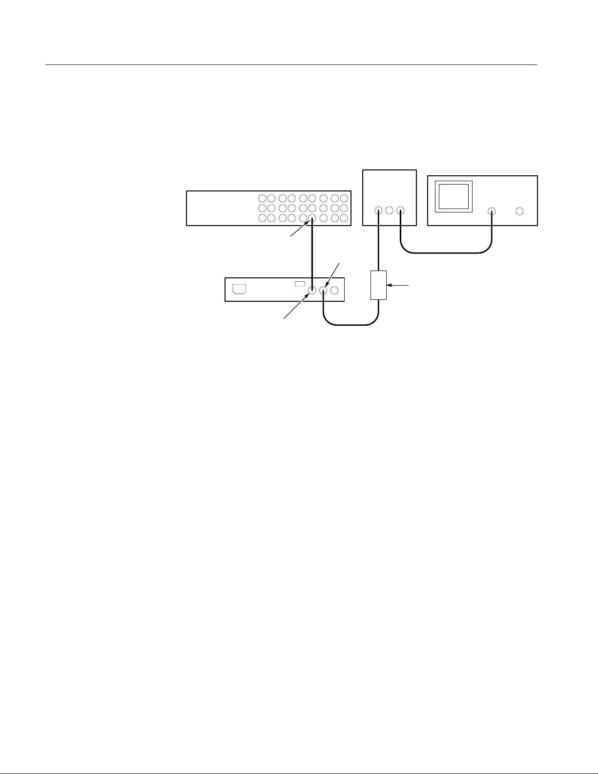
Performance Verification
9. Connect the coaxial cable from the TSG/SPG multiburst output to the VITS
inserter PROGRAM IN. See Figure 5–12.
Peak-to-peak
detector
TSG/SPG
OUTPUTINPUT
Multiburst
Out
Program Out
VITS Inserter
Peak-to-peak
detector head
Program In
Test oscilloscope
Auto VIRS Insertion
Figure 5–12: Measuring frequency response
10. Connect the coaxial cable from the peak-to-peak detector head input to the
VITS inserter PROGRAM OUT.
11. Check that the sweep envelope matches the previous waveform 4.3 mV
from 2 MHz to 6 MHz (second marker to fourth marker). See Figure 5–11.
12. Check that the sweep waveform top matches the waveform measured in
step 7 (the “pattern”) within 12.9 mV from 6 MHz to 10 MHz (fourth
marker to sixth marker). See Figure 5–11.
13. Move the Peak-to-Peak Detector Head and cable from PROGRAM OUT to
MONITOR OUT.
14. Check that the sweep envelope matches the pattern 4.3 mV from 2 MHz
to 6 MHz (second marker to fourth marker). See Figure 5–11.
15. Check that the sweep envelope matches the pattern 12.9 mV from 6 MHz
to 10 MHz fourth marker to sixth marker). See Figure 5–11.
Requirement: Proper VIRS insertion
1. Connect a 75 W coaxial cable from the TSG/SPG black burst output to the
VITS inserter PROGRAM IN.
5–22
2. Connect a 75 W coaxial cable from the VITS inserter PROGRAM OUT to
the waveform/vector monitor input. Terminate the remaining side of the
loop-through connector with a 75 W end-line terminator.
VITS100 NTSC VITS Inserter Instruction Manual
Page 95

Performance Verification
3. Set the waveform/vector monitor line select to line 19, all fields.
4. Check for VIRS. If there is a signal other than VIRS, you will need to either
reprogram the TSG/SPG VITS signals or find a VIRS signal on another line.
VIRS is required on both fields.
5. Set VITS selection switch S2, segments 1 through 4, to 0011 (segments 1
and 2 closed, 3 and 4 open).
6. Confirm that S4 segments 1, 2, 3, and 4 are all open (1111).
7. Turn off the TSG/SPG power switch.
8. Using the waveform/vector monitor line and field selection switches, verify
that the VIRS signal is on field 1 and missing on field 2.
Source ID
Remote Control
Requirement: 16 asserted bits 0.5 V
1. Check and note the position of all rear-panel SOURCE ID switches. These
switches determine the source identification output by the VITS inserter;
restore the original settings after completing this check.
2. Set all 16 switches to the down position.
3. Set VITS inserter line/field selection switch S1, segments 5 through 8, to
0111 (segment 5 closed and segments 6, 7, and 8 open).
4. Select line 18, field 1, on the waveform/vector monitor.
5. Check that there are 16 positive excursions (from 0 V) of approximately
0.5 V. (Instruments with serial numbers below B020425 will have excursions
of approximately 0.7 V.)
6. Switch the waveform/vector monitor Field selection to field 2 and check that
the source ID signal is not present.
Requirement: Grounding pin 6 of the rear-panel REMOTE connector forces the
instrument into bypass mode.
1. Connect a 75ĂW coaxial cable from the VITS inserter PROGRAM OUT to
the waveform/vector monitor Ch A input. Terminate the remaining side of
the loop-through input with a 75ĂW end-line terminator.
2. Set the waveform/vector monitor line select to line 19, field 1.
3. Check that the VIRS signal is displayed on the waveform/vector monitor.
4. Use a short piece of wire to short pin 6 of the rear-panel REMOTE connector
to ground. (Pins 1, 4, and 9 of the REMOTE connector are ground.)
VITS100 NTSC VITS Inserter Instruction Manual
5–23
Page 96

Performance Verification
5. Check that the VIRS signal disappears and the VITS inserter front-panel
BYPASS light comes on.
6. Remove the grounding wire.
7. Check that the VIRS signal reappears and the VITS inserter front-panel
BYPASS light goes out.
5–24
VITS100 NTSC VITS Inserter Instruction Manual
Page 97

Adjustment Procedure
Page 98

Page 99

Adjustment Procedures
If VITS100 NTSC VITS Inserter performance is not within tolerance for a
particular characteristic, determine the cause, repair if necessary, and then use the
appropriate adjustment procedure to return the instrument operation to performance specification. After any adjustment, verify performance by repeating the
applicable part of the Performance Verification procedure.
Allow the instrument to warm up for at least 20 minutes in an ambient temperature of 20° C to 30° C before making any adjustments. Waveform illustrations in
the procedure are typical and may differ from one instrument to another. These
waveforms should not be construed as being representative of specific tolerances.
Static Discharge Precautions
Many semiconductor components, especially MOS types, can be damaged by
static discharge. Damage may not be catastrophic and, therefore, not immediately
apparent. It usually appears as a degradation of the semiconductor characteristics.
Devices that are particularly susceptible are MOS, CMOS, JFETs, and high
impedance operational amplifiers (FET input stages). The damaged parts may
operate within acceptable limits over a short period, but their reliability may be
severely impaired. Damage can be significantly reduced by observing the
following precautions during performance of the adjustment procedure.
H Handle equipment containing static sensitive components or circuit
assemblies at or on a static free work surface. Work stations should contain a
static free bench cover or work plane such as conductive polyethylene
sheeting and a grounding wrist strap. The work plane should be connected to
earth ground.
H All test equipment and accessories should be connected to earth ground.
More information about handling static sensitive assemblies and components can
be found in the Maintenance section of this manual.
Recommended Test Equipment
Table 6–1 lists test equipment and fixtures recommended for the adjustment
procedure. The characteristics specified are the minimum required for the checks.
Substitute equipment must meet or exceed these characteristics.
VITS100 NTSC VITS Inserter Instruction Manual
6–1
Page 100

Adjustment Procedures
T able 6–1: Recommended Test Equipment
Item Minimum Requirements Example
Variable Autotransformer Variable range of 90 to 120 VAC (220 VAC
operation use 220 Vac autotransformer)
Waveform/Vector Monitor Combination waveform monitor and
vectorscope capable of displaying line-rate
and field-rate signals
Television T est Signal Generator NTC7 Composite, Flat Field, Multiburst,
and Red Field signals
Television Test Signal Generator/Sync
Pulse Generator (TSG/SPG)
T est Oscilloscope Vertical amplifier bandwidth of 40 MHz,
Oscilloscope 10X Probe Tektronix P6137 10X Probe
Frequency Counter Counter to measure frequencies up to
Frequency Standard Oscillator with an accuracy of 1 X 10
Peak-to-Peak Detector and Detector Head Amplitude of up to 1 V
Video Noise Generator White noise on composite video, signal-to-
Multimeter Accuracy of +0.7% to measure 0–20 VDC. T ektronix DM252
Power Module Power supply for Frequency Counter,
75 W End-Line Terminators (two) BNC-type terminators, accuracy of 0.25% Tektronix part number 01 1-0102-01
75 W Feed-Through Terminator BNC-type terminator, accuracy of 0.2%. Tektronix part number 011-0103-02
BNC Adaptor Female-to-Female Tektronix part number 103-0028-00
75 W BNC Cables (five) T ektronix part number 012-0159-00
Generator that can output a high frequency
multiburst signal.
1 mV sensitivity, and 0.25% accuracy.
Horizontal time base of 5 msec/div to
2 msec/div and external triggering.
30 MHz ECL levels, with 10 Hz accuracy at
28.6 MHz
–9
(WWV receiver in the USA)
and a flatness of
+0.2% from 50 kHz to 10 MHz
noise ratio of at least 28 dB, Hum noise on
composite video with a 0 dB signal-to-noise
ratio, 1 dB steps with DC coupling, 75 W
impedance, and flat response to 5.5 MHz.
Peak-to-Peak Detector, Video Noise
Generator, and Multimeter
p-p
General Radio metered auto transformer:
W10MT3W.
Tektronix 1780R Video Measurement Set
Tektronix TSG-170A NTSC T elevision
Generator
—
Tektronix TAS465
Tegam DC503A a Universal Counter/Timer
Tektronix part number 015-0408-00
—
Tegam TM506A Power Module Mainframe
Adjustment Procedure
6–2
This procedure is written to accommodate partial or full readjustment. In some
cases only one or two adjustments may be required to return the instrument to
operation within its stated specifications. In these cases you need only adjust the
portion of the VITS inserter that does not meet specifications.
VITS100 NTSC VITS Inserter Instruction Manual
 Loading...