

Page 1

TMSST2
LGA771, 775, and PGA604 Socket
Hardware Support
Instruction Manual
(Includes TMSDPH2 SOCKET T/J 771/775 LGA
Installation instructions)
Confidential
This material is confidential to Tektronix, Intel, and
customers covered by a nondisclosure agreement.
www.tektronix.com
071-1665-01
Page 2

Copyright © Tektronix. All rights reserved. Licensed software products are owned by Tektronix or its subsidiaries or suppliers, and are protected by national copyright laws and international treaty provisions.
Tektronix products are covered by U.S. and foreign patents, issued and pending. Information in this publication supercedes that in all
previously published material. Specifications and price change privileges reserved.
TEKTRONIX and TEK are registered trademarks of Tektronix, Inc.
Contacting Tektronix
Tektronix, Inc.
14200 SW Karl Braun Drive
P.O. Box 500
Beaverton, OR 97077
USA
For product information, sales, service, and technical support:
H In North America, call 1-800-833-9200.
H Worldwide, visit www.tektronix.com to find contacts in your area.
Page 3

Warranty 9(b)
Tektronix warrants that the media on which this software product is furnished and the encoding of the programs on the media will be free
from defects in materials and workmanship for a period of three (3) months from the date of shipment. If any such medium or encoding
proves defective during the warranty period, Tektronix will provide a replacement in exchange for the defective medium. Except as to the
media on which this software product is furnished, this software product is provided “as is” without warranty of any kind, either express or
implied. Tektronix does not warrant that the functions contained in this software product will meet Customer’s requirements or that the
operation of the programs will be uninterrupted or error-free.
In order to obtain service under this warranty, Customer must notify Tektronix of the defect before the expiration of the warranty period. If
Tektronix is unable to provide a replacement that is free from defects in materials and workmanship within a reasonable time thereafter,
Customer may terminate the license for this software product and return this software product and any associated materials for credit or
refund.
THIS WARRANTY IS GIVEN BY TEKTRONIX WITH RESPECT TO THE PRODUCT IN LIEU OF ANY OTHER WARRANTIES,
EXPRESS OR IMPLIED. TEKTRONIX AND ITS VENDORS DISCLAIM ANY IMPLIED WARRANTIES OF MERCHANTABILITY OR
FITNESS FOR A PARTICULAR PURPOSE. TEKTRONIX’ RESPONSIBILITY TO REPLACE DEFECTIVE MEDIA OR REFUND
CUSTOMER’S PAYMENT IS THE SOLE AND EXCLUSIVE REMEDY PROVIDED TO THE CUSTOMER FOR BREACH OF THIS
WARRANTY. TEKTRONIX AND ITS VENDORS WILL NOT BE LIABLE FOR ANY INDIRECT, SPECIAL, INCIDENTAL, OR
CONSEQUENTIAL DAMAGES IRRESPECTIVE OF WHETHER TEKTRONIX OR THE VENDOR HAS ADVANCE NOTICE OF THE
POSSIBILITY OF SUCH DAMAGES.
Page 4

Warranty 2
Tektronix warrants that this product will be free from defects in materials and workmanship for a period of one (1) year from the date of
shipment. If any such product proves defective during this warranty period, Tektronix, at its option, either will repair the defective product
without charge for parts and labor, or will provide a replacement in exchange for the def ective product. Parts, modules and replacement
products used by Tektronix for warranty work may be new or reconditioned to like new performance. All replaced parts, modules and
products become the property of Tektronix.
In order to obtain service under this warranty, Customer must notify Tektronix of the defect before the expiration of the warranty period
and make suitable arrangements for the performance of service. Customer shall be responsible for packaging and shipping the defective
product to the service center designated by Tektronix, with shipping charges prepaid. Tektronix shall pay for the return of the product to
Customer if the shipment is to a location within the country in which the Tektronix service center is located. Customer shall be responsible
for paying all shipping charges, duties, taxes, and any other charges for products returned to any other locations.
This warranty shall not apply to any defect, failure or damage caused by improper use or improper or inadequate maintenance and care.
Tektronix shall not be obligated to furnish service under this warranty a) to repair damage resulting from attempts by personnel other than
Tektronix representatives to install, repair or service the product; b) to repair damage resulting from improper use or connection to
incompatible equipment; c) to repair any damage or malfunction caused by the use of non-Tektronix supplies; or d) to service a product
that has been modified or integrated with other products when the effect of such modification or integration increases the time or difficulty
of servicing the product.
THIS WARRANTY IS GIVEN BY TEKTRONIX WITH RESPECT TO THE PRODUCT IN LIEU OF ANY OTHER WARRANTIES,
EXPRESS OR IMPLIED. TEKTRONIX AND ITS VENDORS DISCLAIM ANY IMPLIED WARRANTIES OF MERCHANTABILITY OR
FITNESS FOR A PARTICULAR PURPOSE. TEKTRONIX’ RESPONSIBILITY TO REPAIR OR REPLACE DEFECTIVE PRODUCTS IS
THE SOLE AND EXCLUSIVE REMEDY PROVIDED TO THE CUSTOMER FOR BREACH OF THIS WARRANTY. TEKTRONIX AND
ITS VENDORS WILL NOT BE LIABLE FOR ANY INDIRECT, SPECIAL, INCIDENTAL, OR CONSEQUENTIAL DAMAGES
IRRESPECTIVE OF WHETHER TEKTRONIX OR THE VENDOR HAS ADVANCE NOTICE OF THE POSSIBILITY OF SUCH
DAMAGES.
Page 5

Table of Contents
General Safety Summary iii.....................................................................
Service Safety Summary v.....................................................................
Environmental Considerations vi..................................................................
Product End-of-Life Handling vi...............................................................
Restriction of Hazardous Substances vi.........................................................
Preface vii..................................................................................
Conventions Used in this Manual vii............................................................
Manual Terms vii..........................................................................
Getting Started 1............................................................................
Logic Analyzer Configuration 1...............................................................
Connect the P6860 Probes and TMSCAB1 Cables 2...............................................
Configure the Preprocessor Unit 3............................................................
Connect the Probe Head to the Target System 7..................................................
Applying and Removing Power 12.............................................................
Replaceable Parts List 13...................................................................
Installing the Software 14....................................................................
Support Package Setup 14...................................................................
Reference 15...............................................................................
Circuit Description 15.......................................................................
Accessories 16...........................................................................
Standard Accessory 16.....................................................................
Optional Accessories 16....................................................................
TMSCAB1 Labels 17.......................................................................
Probe Adapter Notes 18.....................................................................
Probe Adapter Notes 18.....................................................................
Maintenance 19..............................................................................
Storage 20..............................................................................
Shipping the Probe Head 22..................................................................
Specifications 23.............................................................................
Reference Voltage 23......................................................................
AC/DC Signaling 25.......................................................................
Strobe Signals 26.........................................................................
Latched Signals 27........................................................................
Certifications and Compliances 30.............................................................
Loading Diagrams
Design Review Checklists 35.................................................................
Table of Contents
31......................................................................
TMSST2 LGA771, 775, and PGA604 Socket Hardware Support
i
Page 6

Table of Contents
Figures
Figure 1: Preprocessor jumper, adjustment, and connector locations 3......................................
Figure 2: Multiple reference voltage averaging 23......................................................
Figure 3: BCLK requirements 25..................................................................
Figure 4: Strobe signal group requirements 26........................................................
Figure 5: Latched signal group requirements 27.......................................................
Figure 6: Mated Samtec load model 31.............................................................
Figure 7: Receiver load model 31..................................................................
Figure 8: Electrical load model for typical signals 32....................................................
Figure 9: Dimensions of the probe head 33..........................................................
Figure 10: Dimensions of the preprocessor unit 34.....................................................
Tables
Table 1: GTLREF Enable jumpers 5..............................................................
Table 2: Reference and termination jumpers 5.......................................................
Table 3: Reference and terminator connectors 6.....................................................
Table 4: Offset voltage adjustments 6.............................................................
Table 5: LGA771/LGA775 jumper 6...............................................................
Table 6: F2 Acquired signal jumper (AD30 for PGA604) 7...............................................
Table 7: Preprocessor airflow clearance 7..........................................................
Table 8: GTLREF reference voltage requirements for the target system 24....................................
Table 9: BCLK requirements for the target system 25...................................................
Table 10: Strobe signal group assignments 26........................................................
Table 11: DSTB strobe signal requirements for the target system 26........................................
Table 12: TMSST2 Latched signal group assignments 27................................................
Table 13: Latched signal requirements for the target system 28............................................
Table 14: Electrical specifications for AC input to the preprocessor unit 29....................................
Table 15: Environmental specifications 29...........................................................
Table 16: General checklist 35...................................................................
Table 17: Electrical checklist 35..................................................................
Table 18: Mechanical checklist 35.................................................................
ii
TMSST2 LGA771, 775, and PGA604 Socket Hardware Support
Page 7

General Safety Summary
Review the following safety precautions to avoid injury and prevent damage to this product or any products connected to it.
To avoid potential hazards, use this product only as specified.
Only qualified personnel should perform service procedures.
While using this product, you may need to access other parts of a larger system. Read the safety sections of the other
component manuals for warnings and cautions related to operating the system.
To Avoid Fire or Personal Injury
Use Proper Power Cord. Use only the power cord specified for this product and certified for the country of use.
Connect and Disconnect Properly. Do not connect or disconnect probes or test leads while they are connected to a
voltage source.
Ground the Product. This product is grounded through the grounding conductor of the power cord. To avoid electric
shock, the grounding conductor must be connected to earth ground. Before making connections to the input or output
terminals of the product, ensure that the product is properly grounded.
General Safety Summary
Observe All Terminal Ratings. To avoid fire or shock hazard, observe all ratings and markings on the product. Consult
the product manual for further ratings information before making connections to the product.
The inputs are not rated for connection to mains or Category II, III, or IV circuits.
Power Disconnect. The power cord disconnects the product from the power source. Do not block the power cord; it
must remain accessible to the user at all times.
Do Not Operate Without Covers. Do not operate this product with c overs or panels removed.
Do Not Operate With Suspected Failures. If you suspect there is damage to this product, have it inspected by
qualified service personnel.
Avoid Exposed Circuitry. Do not touch exposed connections and components when power is present.
Do Not Operate in Wet/Damp Conditions.
Do Note Operate in an Explosive Atmosphere.
Keep Product Surfaces Clean and Dry.
Provide Proper Ventilation.
proper ventilation.
Refer to the manual’s installation instructions for details on installing the product so it has
TMSST2 LGA771, 775, and PGA604 Socket Hardware Support
iii
Page 8

General Safety Summary
Terms in this Manual
These terms may appear in this manual:
WARNING. Warning statements identify conditions or practices that could result in injury or loss of life.
CAUTION. Caution statements identify conditions or practices that could result in damage to this product or other property.
Symbols and Terms on the Product
H DANGER indicates an injury hazard immediately accessible as you read the marking.
H WARNING indicates an injury hazard not immediately accessible as you read the marking.
H CAUTION indicates a hazard to property including the product.
The following symbol(s) may appear on the product:
CAUTION
Refer to Manual
WARNING
High Voltage
Protective Ground
(Earth) Terminal
Mains Disconnected
OFF (Power)
Mains Connected
ON (Power)
iv
TMSST2 LGA771, 775, and PGA604 Socket Hardware Support
Page 9

Service Safety Summary
Only qualified personnel should perform service procedures. Read this Service Safety Summary and the General Safety
Summary before performing any service procedures.
Do Not Service Alone. Do not perform internal service or adjustments of this product unless another person capable of
rendering first aid and resuscitation is present.
Disconnect Power. To avoid electric shock, switch off the instrument power, then disconnect the power cord from the
mains power.
Use Care When Servicing With Power On. Dangerous voltages or currents may exist in this product. Disconnect
power, remove battery (if applicable), and disconnect test leads before removing protective panels, soldering, or replacing
components.
To avoid electric shock, do not touch exposed connections.
Service Safety Summary
TMSST2 LGA771, 775, and PGA604 Socket Hardware Support
v
Page 10

Environmental Considerations
Environmental Considerations
This section provides information about the environmental impact of the product.
Product End-of-Life Handling
Observe the following guidelines when recycling an instrument or component:
Equipment Recycling. Production of this equipment required the extraction and use of natural resources. The
equipment may contain substances that could be harmful to the environment or human health if improperly handled at the
product’s end of life. In order to avoid release of such substances into the environment and to reduce the use of natural
resources, we encourage you to recycle this product in an appropriate system that will ensure that most of the materi als
are reused or recycled appropriately.
The symbol shown to the left indicates that this product complies
with the European Union’s requirements according to Directive
2002/96/EC on waste electrical and electronic equipment
(WEEE). For information about recycling options, check the Support/Service section of the Tektronix Web site (www.tektronix.com).
Restriction of Hazardous Substances
This product has been classified as Monitoring and Control equipment, and is outside the scope of the 2002/95/EC RoHS
Directive. This product is known to contain lead, cadmium, mercury, and hexavalent chromium.
vi
TMSST2 LGA771, 775, and PGA604 Socket Hardware Support
Page 11

Preface
This document contains specific information about the TMSST2 LGA771, 775, and PGA604 Socket microprocessor
support products and contains information on how to operate this product on compatible Tektronix logic analyzers.
If you are familiar with operating microprocessor support product with the logic analyzer, you need only this manual to set
up and run the probe adapter (processor unit and probe head).
Conventions Used in this Manual
The following icons are used throughout this manual:
Preface
Sequence
Step
1
Manual Terms
The manual uses the following terms:
H GTLREF (Gunning Transceiver Logic Reference)
The GTL+ inputs require a reference voltage (GTLREF) which is used by the receivers to determine if a signal is a
logical 0 or 1.
H Land
Land is an alternate name for a pin and is associated with LGA (land grid array) socket pads on a circuit board.
H Reference voltage
The voltage threshold on the input receivers of the preprocessor unit.
H Termination voltage
The voltage to which the receive signals are terminated.
Pin 1
on a circuit
board
TMSST2 LGA771, 775, and PGA604 Socket Hardware Support
vii
Page 12

Preface
viii
TMSST2 LGA771, 775, and PGA604 Socket Hardware Support
Page 13

Getting Started
The probe adapter (preprocessor unit and probe head) is an interposer design that allows the logic analyzer to acquire data
from a microprocessor in the operating environment with little effect on the target system.
To accomplish this, the probe adapter is connected to the target system, and then the microprocessor is connected to the
probe head. Signals from the microprocessor-based system flow through the probe cables to the logic analyzer.
The TMSST2 product includes:
H CD-ROM with PUB32G11 software and manual (PDF)
H TMSST2 preprocessor unit
NOTE. To acquire signals from the target system, you need compatible cables, probes, and probe head to complete the
connection between the logic analyzer and the target system. Contact your Tektronix sales representative for information
about these other products.
For optional and standard accessories for this product, see Accessories on page 16.
Getting Started
For a list of replaceable parts, see page 13.
Logic Analyzer Configuration
To use the preprocessor unit and probe head to acquire most signals, you need a Tektronix logic analyzer with four merged
TLA7AX4,
All signals are acquired through a combination of P6860 probes and TMSCAB1 cables connected to the logic analyzer.
The P6860 probes should already be labeled; if you need to apply labels, refer to the instructions that came with your
probe documentation.
Refer to the P6810, P6860, and P6880 Logic Analyzer Probes Instruction manual, Tektronix part number 071-1059-xx, for
more information about the P6860. Access the latest version of the manual from the Tektronix.com Web site.
Master and Slave Module Configuration
The modules must be configured and
merged as shown.
HThe memory depth is automatically based
on the shallowest memory depth of the
modules.
HThe term Master module refers to the
second module of a 4-wide module
configuration. The term Slave module
refers to the modules to the left or right of
the Master module.
450 MHz, logic analyzer modules.
S
L
A
V
E
2
M
A
S
T
E
R
S
L
A
V
E
1
S
L
A
V
E
3
TMSST2 LGA771, 775, and PGA604 Socket Hardware Support
1
Page 14

Getting Started
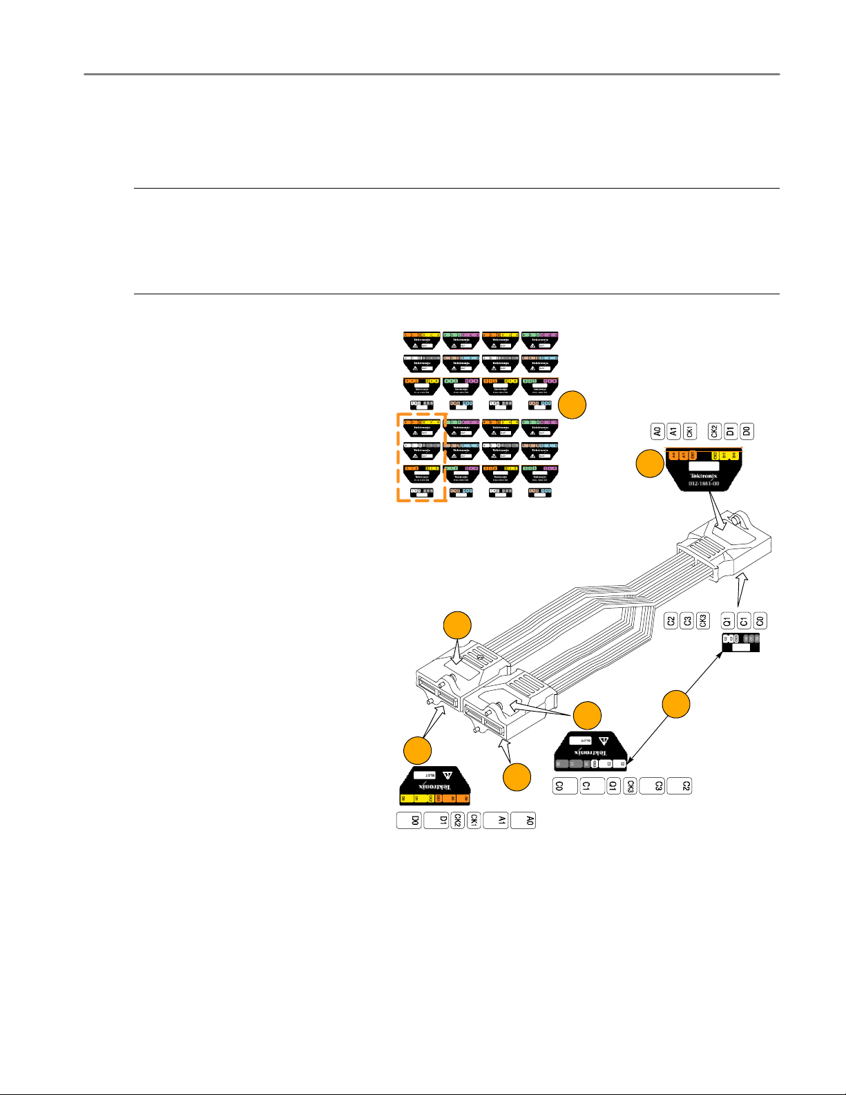
Connect the P6860 Probes and TMSCAB1 Cables
CAUTION. To prevent damage to the probe and preprocessor unit, always position the probes perpendicular to the
footprint on the circuit board. Incorrect handling of the probe while connecting to or disconnecting from the preprocessor
unit can damage the probe.
Use two P6860 probes and five TMSCAB1
cables to connect the TLA7AX4 logic analyzer
modules to the preprocessor unit. If you need to
attach labels to TMSCAB1 cables, refer to
page 17.
TMSCAB1 Cables
1. From the Master module, match the label on
the TMSCAB1 cable with the corresponding
connector label on the preprocessor unit and
connect the cable. The TMSCAB1 cable
connector is keyed for correct alignment to
the preprocessor unit.
1
S
L
A
V
E
3
2
M
A
S
T
E
R
S
L
A
V
E
1
S
L
A
V
E
3
4
2. Use care to evenly tighten both screws on
the module end of the probes or cables until
they are snug. First slightly tighten both
screws, then snug each screw to 4 in--lbs
(max).
3. Repeat step 1 to attach the TMSCAB1
cables to the Slave1 and Slave2 modules.
P6860 Probes
4. Match the A, D, C, and E probes from the
Slave3 and Master module with the corresponding D3/D2 and A3/A2, D1/D0 and
A1/A0, C1/C0 and C3/C2, and E3/E2 and
E1/E0 connector labels on the preprocessor
unit. The P6860 probe connector is keyed for
correct alignment to the preprocessor unit.
Quick Tip. To prevent faulty connections and
loss of data, check that the probe board
connections are clean and free of debris.
1
4
3
2
TMSST2 LGA771, 775, and PGA604 Socket Hardware Support
Page 15

Configure the Preprocessor Unit
To acquire the necessary signals from the target system, the preprocessor unit generates two tracking voltages referred to
TERM
and V
REF.VTERM
as V
reference to which the attenuated target signals are compared.
You can configure the preprocessor unit to use one or more of the GTLREF signals and combine these signals with an
offset voltage using the jumpers on top of the preprocessor unit. (See Figure 1.)
Review the schematic diagram in Figure 1 to understand how the jumpers and offset adjustments define the reference and
termination signals. The connectors provide access for monitoring the voltages.
Connectors
is the voltage to which most of the received target signals are terminated, while V
Schematic diagram of connectors,
jumpers, and offset adjustment circuitry
Getting Started
is the
REF
GTLREF
and offset
jumpers
Offset
adjustments
Figure 1: Preprocessor jumper, adjustment, and connector locations
TMSST2 LGA771, 775, and PGA604 Socket Hardware Support
3
Page 16

Getting Started
Select a GTLREF Signal
The most common and straightforward scenario is to select an individual GTLREF signal using the jumpers to generate a
reference and termination voltage. When you enable a GTLREF signal, the average voltage is equal to the GTLREF
voltage.
As an alternative to a single GTLREF selection, you can combine two or more GTLREF signals that result in the average
of all the contributors. The next step beyond a GTLREF only selection is to add a DC offset. The resultant voltage
continues to track GTLREF. Refer to the following combined calculation:
or V
V
REF
TERM
= ((V
OFFSET
-- V
GTLREF_AVG
) x 0.130) + V
GTLREF_AVG
If you choose only the offset voltage to define the termination or reference voltage, a weighting factor is not used and the
full magnitude offset voltage defines the resultant voltage.
For example, you selected a GTLREF signal that equals 0.7 V, the AVERAGE GTLREF jumper is enabled, and you are
using an offset voltage to provide +0.05 V of offset. The resultant voltage would be 0.75 V.
To set this offset voltage, adjust to:
V
OFFSET
=7.69(V
RESULT
-- V
GTLREF_AVG
)+V
GTLREF_AVG
= 7.69 (0.75--0.70) + 0.70
= 1.0845 V
To summarize, the offset voltage source must be at 1.08 V to provide the +0.05 V of offset (in combination with an
averaged GTLREF signal equal to 0.7 V). Therefore, if the AVERAGE GTLREF jumper is moved to the disabled position,
an offset only selection sets the resultant voltage at 1.08 V.
NOTE. All jumpers and connectors are located on top of the preprocessor unit.
4
TMSST2 LGA771, 775, and PGA604 Socket Hardware Support
Page 17

Average a GTLREF Signal
EnableH2F23
2--3Disablepin
1
To average GTLREF signals, enable one or more of the GTLREF jumpers. (See Table 1.)
Table 1: GTLREF Enable jumpers
LGA771 and 775
Jumpers
Microprocessor pin
name
PGA604
Microprocessor pin name
Getting Started
Default
pin position
--
B
H1 F9 1--2 Enable
E24 W23 2--3 Disable
F2 AD30 2--3 Disable
G10 W9 2--3 Disable
Combine Averaged GTLREF Signals with Offset Voltages
Use the four sets of jumpers shown in Table 2 to combine the averaged GTLREF signal with a separate independent fixed
offset voltage.
H Enable both sets of REFERENCE jumpers to generate a combined reference voltage.
H Enable both sets of TERMINATION jumpers to generate a combined termination voltage.
Table 2: Reference and termination jumper s
Jumpers Jumper name Default pin position
Enable
pin 1
B
REFERENCE
USE OFFSET
2--3 Exclude
USE AVERAGE GTLREF
1--2 Include
TERMINATION
USE OFFSET
USE AVERAGE GTLREF
2--3 Exclude
1--2 Include
When you enable both the AVERAGE GTLREF and the OFFSET jumpers, the resultant termination and reference
voltages are weighted (20 to 3) to provide a substantial degree of GTLREF tracking.
Even when the AVERAGE GTLREF jumper is disabled for both the reference and termination voltage, the average
GTLREF signal is used to generate a reference voltage for 13 target signals. To guarantee that the average GTLREF
signal is at an appropriate level, the average GTLREF signal defaults to the processor land H1 on the target system, if all
five jumpers are placed in the disabled position.
TMSST2 LGA771, 775, and PGA604 Socket Hardware Support
5
Page 18

Getting Started
TERMINATIONAVERAG
E
TERMINATIONOFFSETADJUST
NOTE. If the land H1 on the target system is the desired GTLREF signal, use the jumper on the preprocessor unit to
enable it rather than relying on defaults. The land H1 default is only intended to prevent undefined conditions from
occurring.
Adjust GTLREF Offset Voltage
To use either reference or termination offset voltage, you must enable it. (See Table 2 on page 5.) Connect a voltmeter to
the Reference or Terminator connector and GND on the preprocessor unit using standard cables. The voltage is the
averaged signal that is used by the front-end comparators (reference average and termination average). If the manual USE
OFFSET jumper is the only jumper enabled, the voltage at the connector directly reflects the manual offset voltage.
CAUTION.
Connecting a voltage source to the Reference or Terminator connectors can damage the
preprocessor unit. Only use standard cables to read the manual offset voltage. (See Table 3.)
Table 3: Reference and terminator connectors
Connectors Name
GND -- MEASUREMENT REFERENCE
REFERENCE AVERAGE
Adjust the offset voltage with a small screwdriver, if necessary. (See Table 4.) Turn the potentiometer clockwise to increase
the voltage. The range of the offset voltage is from 0.4 V to 1.0 V.
Table 4: Offset voltage adjustments
Adjustment Name
TERMINATION OFFSETADJUST
REFERENCE OFFSET ADJUST
NOTE. To resolve acquisition errors, adjust the reference voltage. To resolve target-system loading issues, adjust the
termination voltage.
LGA771/LGA775 jumper. Select the socket that your target processor uses.
Table 5: LGA771/LGA775 jumper
Socket name Pin position
PGA604 1--2 (default)
LGA775 1--2 (default)
LGA771 2--3
6
TMSST2 LGA771, 775, and PGA604 Socket Hardware Support
Page 19

Getting Started
F2 ACQUIRED SIGNAL jumper.
default.
Enable REF if the signal is a GTLREF signal, otherwise ACQUIRED SIGNAL is the
Table 6: F2 Acquired signal jumper (AD30 for PGA604)
Jumper name Pin position
Acquired signal 1--2 (default)
REF 2--3
XTGIP and Test Ports. Not used.
Connect the Probe Head to the Target System
CAUTION. To prevent static damage to the microprocessor, preprocessor unit, probe head, probes, and module, handle
components only in a static-free environment. Always wear a grounding wrist strap, heel strap, or similar device while
handling the microprocessor and probe adapter.
WARNING. To prevent personal injury or damage to the preprocessor unit, do not open the preprocessor unit. There are
no operator-serviceable parts inside the preprocessor unit. Refer servicing of internal parts in the preprocessor unit to
Tektronix authorized personnel only. External parts may be replaced by qualified service personnel.
Airflow Clearance
Table 15 lists airflow clearances on all sides of the preprocessor unit.
Table 7: Preprocessor airflow clearance
Side of the unit Required clearance
Required airflow clearances for the
preprocessor
Front, top, left side 5.08 cm (2 in)
Back 7.60 cm (3 in)
Bottom, right side 0.635 cm (0.250 in)
Required Tools
H Use a flatbladed screwdriver (0.1 inch tip width) to tighten the probe head to the target system.
Optional Tool
H A torque wrench helps to ensure reliable connections by meeting the nominal torque values. Unless noted otherwise, tighten
screws to 8 in-lbs.
TMSST2 LGA771, 775, and PGA604 Socket Hardware Support
7
Page 20

Getting Started
CAUTION. To prevent damage to the LGA771 and 775 socket, minimize the amount of times the processor is inserted into
the probe head. The probe head is designed to withstand 20 processor insertions. Once the LGA771 or 775 socket is
damaged, the probe head cannot be repaired. If great care is taken during processor insertion, the cycle life of the probe
may be extended.
Use the following steps to install parts:
Probe Head Installation
CAUTION. To prevent damage to the socket,
do not touch the springs in the socket.
NOTE. To connect the TMSSPH1 probe head,
see the TMSSPH1 PGA604 Socket F Hardware
Support Manual (071-2001-XX).
Use the following steps to connect the
TMSDPH2 probe head to the target system.
1. Power off the target system. It is not nec-
essary to power off the logic analyzer.
2. Power off any probe heads (or prepro-
cessor unit) that may be attached to the
target system.
3. Open the load lever.
4. Open and remove the load plate.
5. Remove the microprocessor from the tar-
get system.
6. Attach the custom load plate.
Load plates are vendor-specific. Use the
load plates marked with an “F” with the
Foxconn socket and the load plate
marked with a “T” with the Tyco socket.
4
3
5
7
6
7. Close the load lever.
8
TMSST2 LGA771, 775, and PGA604 Socket Hardware Support
Page 21

Getting Started
Use the following steps to connect the microprocessor to the probe head socket:
CAUTION. To prevent damage to the springs
in the processor socket or damage to the
preprocessor unit caused by power and
ground shorts, check that the pin 1 indicator
on the probe head aligns with the pin 1
indicator on the target system. (See the
additional Caution on page 8.)
8. Open the load lever and load plate on
the probe head.
9. Remove the socket cover.
10. Install the microprocessor, carefully align-
ingpin1indicators(
").
8
9
10
11. Close the load plate.
12. Close the load lever.
12
TMSST2 LGA771, 775, and PGA604 Socket Hardware Support
11
9
Page 22

Getting Started
1
Use the following steps to connect the probe
head to the target system:
Check the following items:
H The bar is positioned as shown
H You have correctly located pin 1
13. Do not remove the socket adapter from
the bottom of the probe head.
14. Attach the probe head to the target sys-
tem carefully aligning pin 1 indicators (
Bar
13
").
14
15. Tighten the two screws to the custom
load plate as shown.
To install the LGA771 heatsink hardware,
see page 11. If your system uses the to
install the LGA775 heat sink kit hardware, follow these steps:
16. Thread the standoffs onto the screws as
shown.
17. Snap the heat sink into the standoffs(4).
18. Connect the probe head cables to the
preprocessor unit cables (snap into
place) paying close attention that the labels on the paddle boards match: A to A,
and so forth.
19. Apply forced-air cooling across the micro-
processor and heat sink to keep the microprocessor from overheating unless
you are using a forced air-cooled heat
sink and fan assembly.
17
18
15
10
TMSST2 LGA771, 775, and PGA604 Socket Hardware Support
Page 23

If your system uses the LGA771 heat sink, follow
these steps to attach the TMSDPH2 probe head
and the LGA771 heat sink kit hardware:
1. Do not remove the socket adapter from
the bottom of the probe.
2. Using the flat head screws, attach two
heat sink bottom brackets to the target
system.
Getting Started
3. Attach two standoffs to the target sys-
tem.
4. Attach the probe head to the target sys-
tem, aligning pin 1 indicators (
5. Dress the cables over the bottom heat
sink bracket.
6. Tighten the two screws to the custom
load plate as shown.
7. Using the pan head screws, attach two
heat sink top brackets as shown.
8. Apply thermal grease to the top of the
copper spacer.
9. Install the heat sink.
10. Connect the probe head cables to the
preprocessor unit cables (snap into
place) paying close attention that the labels on the paddle boards match: A to A,
and so forth.
").
10
2
1
3
4
9
7
8
11. Apply forced-air cooling across the micro-
processor and heat sink to keep the microprocessor from overheating unless
you are using a forced air-cooled heat
sink and fan assembly.
TMSST2 LGA771, 775, and PGA604 Socket Hardware Support
5
6
11
Page 24

Getting Started
Probe Head Removal
Follow these steps to remove the probe head
from the target system:
CAUTION. To prevent damage to the springs
in the probe-head socket, always insert the
socket cover when the probe head is not in
use. (See Step 9 on page 9.)
1. Power off the target system, and unplug
the AC power cord from the preprocessor
unit. The power switch for the preprocessor unit is located on the back of the preprocessor unit. It is not necessary to
power off the logic analyzer.
2. Reverse the steps in the previous illustra-
tions to remove the probe head.
3. Store the probe head.
2
Applying and Removing Power
To apply power to the preprocessor unit and
target system, follow these steps
1. Make sure the power switch on the pre-
processor unit is in the off position. When
powered off, the zero (0) is visible on the
power switch.
2. Plug the AC power cord into the IEC con-
nector on the back of the preprocessor
unit.
3. Plug the AC power cord into an electrical
outlet.
4. Power on the preprocessor unit using the
switch at the back of the preprocessor
unit. A green, power-on LED lights on the
front of the preprocessor unit, indicating
that the preprocessor unit is active.
5. Power on the target system.
To remove power from the target system
and the preprocessor unit, reverse the
preceding steps.
:
1
12
TMSST2 LGA771, 775, and PGA604 Socket Hardware Support
Page 25

Replaceable Parts List
Refer to the following table to view and reorder replaceable parts for the preprocessor and probe head.
Getting Started
Page number
8 4 1 Load plate, bottom, for FOXCONN socket 386-7398-XX
8 4 1 Load plate, bottom, for Tyco socket 386-7400-XX
9 9 1 Socket cover 200-4843-XX
10 13 1 Socket adapter; SMD, BGA to LGA, pin header, 769 POS 131-7494-XX
2 1 1 Cable assembly (for preprocessor unit) with labels 012-1661-51
1
To order replaceable parts for the heat sink kits or other probe heads, refer to the instructions that came with that
product.
NOTE. For a list of standard and optional accessories (including heat sink kits), refer to page 16 .
Step Quantity Description Part number
1
TMSST2 LGA771, 775, and PGA604 Socket Hardware Support
13
Page 26
Getting Started
Installing the Software
NOTE. Before you install any software, verify
that the microprocessor support software is
compatible with the logic analyzer software
by comparing the version number on the CD
to the Tektronix logic analyzer system
software.
To install the TMSST2 software on the
Tektronix logic analyzer, follow these steps:
1. Insert the CD in the CD drive.
2. Follow the on-screen instructions to
install the software.
To remove or uninstall software, use the Add
or Remove Programs utility in the Windows
Control Panel. Close all windows before you
uninstall any software.
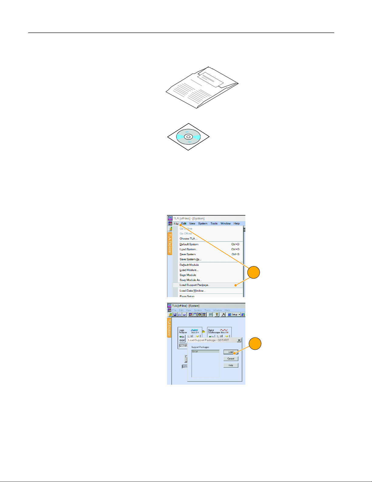
Support Package Setup
After installing the software, you need to load
the PUB32G11 setup file. Follow these
steps:
1. From the file menu, open a logic analyzer system window and select Load Support Package.
2. In the Load Support Package dialog box,
select the support and click load.
3. Follow the on-screen instructions.
1
2
14
TMSST2 LGA771, 775, and PGA604 Socket Hardware Support
Page 27

Reference
Circuit Description
The preprocessor unit and probe head processes all signals on the microprocessor before the logic analyzer captures the
signals. The TMSST2 product performs the following functions:
H Latches signals within a narrow valid window
H Demultiplexes quad-pumped, source-synchronous signals
H Deterministically synchronizes source-synchronous data signals to BCLK
Latched Operation
The signals are processed according to their type. Following is a description of each type:
4x Quad-Pumped Signals. These signals include D[63:00]# and DBI[3:0]#. The signals are latched using dedicated
strobes, STBP[3:0] and STBN[3:0], and then four-way demultiplexing is performed on these signals. The LAI inverts the
appropriate signals when the DBI[3:0] signals are active.
Reference
2x Double-Pumped Signals. These signals include A[39:03]# and REQ[4:0]#. The LAI buffers and restores these
signals. It then sends the signals to the logic analyzer along with ADSTB[0] to be multiplexed into the common clock
domain. The logic analyzer uses the ADS to deterministically place these signals into the correct clock frame.
1x Common-Clock Signals. These signals include all of the remaining front side bus signals. The logic analyzer
latches these signals using the rising edge of BCLK.
Signal Probing
The probe head uses passive series isolation to acquire data.
GTLREF Jumper Settings
The preprocessor unit uses reference voltages from the target system to derive a signal called GTLREF_AVG. This voltage
is used as a reference to acquire most signals from the target system. The preprocessor unit can average up to five
reference voltages and a manual offset voltage. See Configure the Preprocessor Unit beginning on page 3.
TMSST2 LGA771, 775, and PGA604 Socket Hardware Support
15
Page 28

Reference
Accessories
Standard Accessory
The following standard accessory is shipped with the TMSST2 preprocessor unit:
Quantity Accessory Part number
1
Software Pkg; V1.020,W/HARDWARE MANUAL;TMSST2
Order-by-description
PUB32G11
Optional Accessories
The following optional accessories are available for the TMSST2 preprocessor unit:
Option Description Part number
--
P6860 PROBES Order-by-description
-- TMSCAB1 CABLES Order-by-description
TMSDPH2 PROBE HEAD BOARD W/CABLES & PADDLE
Order by description
BD,SOCKET T/J 771/775 LGA
-- Software Pkg; V1.020 NDA SW & HW MANUALS; TMS119 IA32G11 Order-by-description
-- ACCESSORY KIT; LGA771 HEAT SINK;TMSDPH2 020-2650-XX
-- ACCESSORY KIT; LGA775 HEAT SINK;TMSDPH2 020-2708-XX
-- TMSSPH1P PROBE HEAD BOARD W/CABLES & PADDLE BD,
Order-by-description
SOCKET F 604 PGA
-- Software Pkg; V1.000, NDA SW & HW MANUALS;TMS125
Order-by-description
IA32G16
-- SHIPPING KIT: CARTON AND FOAM 065-0701-XX
-- PLASTIC STORAGE CASE WITH FOAM INSERTS AND FLEX
016-1940-XX
CABLE ASSEMBLY
A0 US POWER CORD. (STANDARD ACCESSORY) 161-0104-00
A1 UNIVERSAL EURO POWER CORD 161-0104-06
A2 UNITED KINGDOM POWER CORD 161-0104-07
A5 SWITZERLAND POWER CORD 161-0167-00
1
Requires six probes
2
Requires five cables
3
This support software is available only to customers with a valid, restricted, and secret nondisclosure agreement
(RS-NDA) with Intel and Tektronix.
1
2
3
3
16
TMSST2 LGA771, 775, and PGA604 Socket Hardware Support
Page 29
TMSCAB1 Labels
If you need to attach labels to the module end and the preprocessor end of theTMSCAB1 cables, use the following
instructions.
NOTE. Always use flat-nosed tweezers to remove the labels from the sheet of labels. Never peel labels with your fingers.
The labels are made of soft vinyl and can stretch and distort easily. To avoid stretching the label, always grasp it from the
top right corner while removing it from the sheet of labels.
The adhesive on the vinyl labels is extremely strong. Carefully ali gn the label to the indented outline on the module end
and preprocessor unit end. Once labels are placed on the TMSCAB1 cables, they are difficult to remove.
Follow these steps to attach the labels:
1. Determine which channel groups you
plan to use and identify the matching labels.
2. Align and place the label in the label in-
dent (preprocessor-unit end).
Reference
1
3. Match the color and the channel name.
4. Align and place the label in the label in-
dent (module end)
5. No label on the underside of this connec-
tor.
6. Align and place the label in the label in-
dent (module end).
7. No label on this side of the connector.
2
7
3
4
6
5
TMSST2 LGA771, 775, and PGA604 Socket Hardware Support
17
Page 30

Reference
Probe Adapter Notes
Probe Adapter Notes
Review electrical, environmental, and mechanical specifications in the Specifications section starting on page 23 because
they pertain to the target system, and to the following information.
Acquisition before Reset. If data is acquired before a processor Reset signal is observed by the preprocessor unit, the
data acquired by the logic analyzer will be inaccurate.
Data Bus. The TMSST2 product supports only a quad-pumped data bus.
Address Bus. The TMSST2 product supports only a double-pumped address bus.
Disabling the Cache (disassembly). The cache bus is not observable; therefore, disassembly requires that the cache
must be disabled. Disabling the cache makes all instruction prefetches visible on the bus so that they are acquired,
displayed, and correctly disassembled.
18
TMSST2 LGA771, 775, and PGA604 Socket Hardware Support
Page 31

Maintenance
Before cleaning this product, read the following information:
CAUTION. To prevent static damage to the microprocessor and the probe head, handle components only in a static-free
environment. Always wear a grounding wrist strap, heel strap, or similar device while handling themicroprocessor and
probe head.
The probe head does not require scheduled or periodic maintenance. However, to keep good electrical contact and
efficient heat dissipation, keep the probe head free of dirt, dust, and contaminants. When not in use, store the probe head
in the original case and cardboard carton.
External Cleaning Only
Clean dirt and dust with a soft bristle brush. For more extensive cleaning, use only a damp cloth moistened with deionized
water; do not use any other chemical cleaning agents.
WARNING. To prevent personal injury or damage to the probe head, do not allow any moisture inside the probe head.
Refer servicing of external parts in the probe head to only Tektronix authorized personnel. External parts may be repl aced
by qualified service personnel.
Maintenance
CAUTION. To prevent damage to the sensitive probe head cables, handle them with care.
TMSST2 LGA771, 775, and PGA604 Socket Hardware Support
19
Page 32

Maintenance
Storage
Short-Term Storage
For short-term storage, use the existing cardboard
carton and packaging, and follow these steps:
1. Power off the target system, and unplug the
AC power cord on the preprocessor unit. It is
not necessary to power off the logic analyzer.
2. Reverse heat sink instructions (for LGA775
or 771 socket) to remove the heat sink.
3. Reverse steps 1 through 15 on page 10 to
remove the probe head, dressing the cables
so they are not pinched or contacting any
sharp objects. When you fold the preprocessor cables use a minimum radius of 0.25-in
(0.64 cm) at the fold.
4. Using non-static generating tape, tape the
socket cover onto the pin header on the bottom of the probe head.
5
5. Store the probe head in the black case it
was shipped in.
20
TMSST2 LGA771, 775, and PGA604 Socket Hardware Support
Page 33

Maintenance
Long-Term Storage
For long-term storage, use the existing cardboard
carton and packaging, and follow these steps:
1. Complete steps 1 through 5 on page 20 in
the Short-Term Storage procedure.
2. Disconnect the preprocessor unit from the
logic analyzer by removing the probes and
TMSCAB1 cables from the top of the preprocessor unit.
3. Place the preprocessor unit and probe head
inside static-shielding bags.
4. Place foam on the bottom and inside of the
cardboard carton.
5. Place the foam end caps on both sides of
the preprocessor unit and place the preprocessor unit inside the cardboard carton.
6. Place cables carefully over the top of the
preprocessor unit.
7. Place probe head and cables in the appropri-
ate cutouts.
3
4
5
6
7
8
8. Place other accessories in the accessory
tray.
9. Close and tape the cardboard carton.
TMSST2 LGA771, 775, and PGA604 Socket Hardware Support
21
Page 34

Maintenance
Shipping the Probe Head
To commercially transport the preprocessor unit and
probe head, package as follows
:
1. Use the existing cardboard shipping carton
and cushioning material. Follow the steps on
page 21 to package the probe head and preprocessor unit
If the existing shipping carton is not available,
use a double-walled, corrugated cardboard
shipping carton that allows a 3-in (7.62 cm)
minimum space on all sides of the product. Fill
this space with nonstatic packing material.
2. If you are shipping a preprocessor unit or
probe head to a Tektronix service center for
warranty service, attach a tag to the product
showing the following:
H Owner’s name and address
H Name of a person who can be con-
tacted
H Probe head type and serial number
H Description of the problem
.
1
2
22
TMSST2 LGA771, 775, and PGA604 Socket Hardware Support
Page 35

Specifications
These specifications are for a probe adapter (preprocessor unit and probe head) that is connected between a compatible
Tektronix logic analyzer and a target system. All specifications are typical. This section also outlines the electrical and
mechanical requirements that the system-design engineer must observe during the planning and designing of their target
system. This planning ensures compatibility with the probe adapter.
NOTE. These specifications can be used with the TMSSPH1 probe head with the exception of the dimensional drawing, or
noted otherwise.
Reference Voltage
Some target systems incorporate multiple reference voltages. These voltages are averaged by the preprocessor unit and
used to receive all signals. Figure 2 shows an example of averaging two different reference voltages.
Specifications
Composite probe
adapter time/voltage
V
REF1
V
REF2
Figure 2: Multiple reference voltage averaging
NOTE. The overall time/voltage eye seen by the probe adapter is reduced when different reference voltages are present in
the target system.
When designing a multiple reference voltage system, the system designer must ensure that the composite eye seen by the
preprocessor unit conforms to the electrical requirements described in this section. All electrical requirements listed in this
section are relative to the averaged reference voltage.
The preprocessor unit provides a user-defined offset that can be added to the averaged reference voltage for flexibility. The
offset function can also be used by itself, and adjusted to a desired fixed voltage. The averaged reference voltage tracks
changes in the references, while the offset is a fixed voltage. To provide a significant amount of tracking while using an
offset, the averaged reference is weighted 20:3 relative to the Offset voltage.
The TMSST2 preprocessor unit generates a separate termination and reference voltage.
With separate reference and termination voltages, it is possible to adjust the termination voltage to optimize target-system
performance with the preprocessor unit installed and active. You can then adjust the reference voltage to optimize the
preprocessor unit operation and achieve error-free acquisition. In most applications, the affect of the probe adapter loading
is low enough to suffice for the simplest case of reference and termination voltages (both being set to the averaged
reference only, no offset). Independent adjustments with or without offsets are available, if needed.
V
REFA
TMSST2 LGA771, 775, and PGA604 Socket Hardware Support
23
Page 36

Specifications
Table 8: GTLREF reference voltage requirements for the target system
Description Min Max
Input voltage range
Input current (DC bias)
Offset voltage range, combined
Offset voltage range, Offset only
Slew Rate
5,7
Edge Rate, 10--90%; ≤50mv step size
Edge Rate, 10--90%; 50mv < step ≤200mv
1
Specifications are relative to the pins on the probe head.
2
AC load modeled as unterminated 275 Ω, 8 ns transmission line.
3
Max Negative Offset = 0.13 x (V
MaxPositiveOffset=0.13x(1.0–V
4
Fixed voltage, no tracking
5
Response is primarily bandwidth rather than slew rate limited.
6
Step response; transitions ²20 μs for step sizes less than 50 μv, ²30 μs for transitions up to 200 μv are stable within
100 μs. Faster transitions require up to 250 μs to stabilize.
7
Because of propagation delay and slew rate differences between V
error-free during reference voltage transitions that violate the Slew Rate or Edge Rate limits
1
2
3
4
0.40 V 1.10 V
-- 0 . 2 μA 0.2 μA
See Note
3
See Note
0.45 V 1.0 V
3
0 1.25 mV/μs
6,7
6,7
GTLREF_AVG
GTLREF_AVG
–0.4);
)
40 μs -- --
50 μs -- --
and V
TERM
REF
, acquisition is not guaranteed to be
.
24
TMSST2 LGA771, 775, and PGA604 Socket Hardware Support
Page 37

AC/DC Signaling
The TMSST2 preprocessor unit divides the front side bus signals into different acquisition groups depending on the
characteristics of each signal. Each signal group is acquired using a different acquisition topology and has unique AC and
DC requirements.
T
BCLK
BCLKn
V BCLK_CM
BCLKp
Figure 3: BCLK requirements
Table 9: BCLK requirements for the target system
1,2,3
Symbol
-- -- -- Common Clock Rate
T
BCLK
V
BCLK_DIFF
V
BCLK_CM
1 Specifications are relative to the pins on the probe head.
Description Min Max
Clock period 3ns
Differential input voltage 200 mV 900 mV
Differential common-mode input range 0.15 V 1.1 V
Specifications
V
BCLK_DIFF
1
100 MHz 333 MHz
4
10 ns
4
2 Uncertainty surrounding the active edge is accounted for in the requirements of the signals that are latched by the active
edge.
3 Signal must be monotonic during transition.
4
TMSSPH1 common clock rate is 267 MHz, 3.75 ns.
TMSST2 LGA771, 775, and PGA604 Socket Hardware Support
25
Page 38

Specifications
Strobe Signals
There are two strobe signal acquisition groups. Each group is defined in the table below, followed by the AC and DC
signaling requirements. Both strobe groups have the same requirements.
Table 10: Strobe signal group assignments
Group Signals Description
DSTB DSTB[3:0]p, DSTB[3:0]n Single-ended, active falling-edge, buffered and used for latching
solely by the preprocessor unit
ADSTB ADSTB[1:0] Single-ended, active on both edges, buffered initially by the
preprocessor unit then used for latching by the LA module
V
MAX
V
V
REFA
IH
V
IL
V
MIN
Figure 4: Strobe signal group requirements
Table 11: DSTB strobe signal requirements for the target system
1,2,3,4
Symbol
V
IH
V
IL
V
MAX
V
MIN
1 Specifications are relative to the pins on the probe head.
2 Uncertainty surrounding the active edge is accounted for in the requirements of the signals that are latched by the active edge.
3 Signal must be monotonic during transition.
4V
are dependant upon the receiver hysteresis setting. Larger hysteresis yields larger delay changes due to changes
IH,VIL
in required overdrive and thus larger Setup and Hold window size. Selected hysteresis is relatively large, thus yielding
substantial noise immunity but requiring a substantial overdrive.
To improve immunity to nonmonotonic anomalies present on the target system strobe signals, the preprocessor and logic
analyzer module employ both voltage and time domain hysteresis.
Description Requirement
Input high voltage (min) V
Input low voltage (max) V
REFA
REFA
+125 mV
--125 mV
Maximum input voltage 1.5 V
Minimum input voltage -- 0 . 2 V
26
For both the DSTB and ADSTB signal groups, the voltage domain hysteresis is adjustable at the factory from 3.5 mV
typical to over 100 mV at the probe tip. The amount of hysteresis applied cannot be changed. The amount of hysteresis is
set to nominally 48 mV (ᐔ24 mV).
The time domain hysteresis is different for the DSTB and ADSTB groups. For the DSTB group, any nonmonotonic
anomaly within 0.8 ns of an incident falling-edge is ignored. For the ADSTB group, any nonmonotonic anomaly within 1250
ps of the incident falling or rising edge is ignored.
TMSST2 LGA771, 775, and PGA604 Socket Hardware Support
Page 39

Latched Signals
Latched signal acquisition groups are defined in Table 12.
Table 12: TMSST2 Latched signal group assignments
Specifications
Group Signals Latching
Description
edge
L1 BNR, BPM[5:0], BPRI, BR[3:0], DBSY, DEFER,
FERR, IERR, LINT[1:0], LOCK, NMI, MCERR,
BCLK 275 Ω load, terminated to V
module
PROCHOT, RSP, THERMTRIP, TRDY
1
L2
LGA771 and 775 sockets: A20M, DPSLP, IGNNE,
INIT, SMI, SLP, STPCLK, TCK, TDI, TDO, TMS, TRST
BCLK 275 Ω load, terminated to 0.75xV
by LA module
(Unterminated) PWRGOOD Unterminated 75 Ω, 8 ns transmission line w/ 200 Ω
series resistor at Interposer
PGA604 socket: A20M, DPSLP, IGNNE, INIT, SMI,
SLP, STPCLK
(Unterminated) TRST, TMS, TDO_M, TDO, TDI_M,
TDI, TCK
BCLK 275 Ω load, terminated to 0.75xV
by LA module
Unterminated 75 Ω, 8 ns transmission line w/ 200 Ω
series resistor at Interposer
L3 ADS, BINIT, DRDY, HIT, HITM, RESET, RS[2:0] BCLK 275 Ω load, terminated to V
preprocessor unit for real-time processing, also latched
by LA module.
L4 A[39:3], REQ[4:0] ADSTB 275 Ω load, terminated to V
module.
L5 D[63:0], DBI[3:0] DSTB 275 Ω load, terminated to V
preprocessor unit for real-time processing.
1
Commonly referred to as CMOS
; latched by LA
TERM
GTLREF_AVG
GTLREF_AVG;
; latched by
TERM
; latched by LA
TERM
; latched by
TERM
, latched
latched
Figure 5 and Table 13 show the requirements for each of the latched acquisition groups. Each group defines a four-point
time/voltage eye that is measured relative to the respective latching edge and V
Figure 5. For example, if you are using Group L1, LX equals L1.
Latching
edge
LX_VB
T
LX_VA
V
V
LX_IH
LX_IL
V
V
V
T
MAX
REFA
MIN
Figure 5: Latched signal group requirements
TMSST2 LGA771, 775, and PGA604 Socket Hardware Support
. LX represents the group name in
REFA
27
Page 40

Specifications
Table 13: Latched signal requirements for the target system
Symbol Description Typical
1,2,3
T
L1_VB
1,2,3
T
L1_VA
1,2,3
V
L1_IH
1,2,3
V
L1_IL
1,2,3
T
L2_VB
1,2,3
T
L2_VA
1,2,3
V
L2_IH
1,2,3
V
L2_IL
1,2,3
T
L3_VB
1,2,3
T
L3_VA
1,2,3
V
L3_IH
1,2,3
V
L3_IL
1,2,3
T
L4_VB
1,2,3
T
L4_VA
1,2,3
V
L4_IH
1,2,3
V
L4_IL
1,2,3
T
L5_VB
1,2,3
T
L5_VA
1,2,3
V
L5_IH
1,2,3
V
L5_IL
1,4
V
MAX
1,4
V
MIN
1,4
V
MAX
1,4
V
MIN
1
Specifications are relative to the pins on the probe head.
2
Assumes nominal signal receiver hysteresis of 5 mV (no added hysteresis)
3
Timing characterized with both a pattern generator and selected target platforms; correlation to operation in the target
environment is approximate due to edge rate and signal quality differences for both the measured signal and its strobe
(clock) for different platforms.
4
Max and Min numbers rely on termination and thus GTLREF specified voltage limits.
L1 valid time before edge 800 ps
L1 valid time after edge 100 ps
L1 input high voltage V
L1 input low voltage V
REFA
REFA
L2 valid time before edge 850 ps
L2 valid time after edge 150 ps
L2 input high voltage 0.75*V
L2 input low voltage 0.75*V
L3 valid time before edge 750 ps
L3 valid time after edge 50 ps
L3 input high voltage V
L3 input low voltage V
REFA
REFA
L4 valid time before edge 750 ps
L4 valid time after edge 50 ps
L4 input high voltage V
L4 input low voltage V
REFA
REFA
L5 valid time before edge 250 ps
L5 valid time after edge 250 ps
L5 input high voltage V
L5 input low voltage V
Maximum input voltage (all signals excluding
REFA
REFA
+1.5 V
unterminated L2)
Minimum input voltage (all signals excluding
-- 0 . 2 V
unterminated L2)
Maximum input voltage
+1.1 V
(unterminated L2)
Minimum input voltage
+0.1 V
(unterminated L2)
+150 mV
--150 mV
GTLREF_AVG
GTLREF_AVG
+150 mV
--150 mV
+125 mV
--125 mV
+75 mV
-- 7 5 m V
+150 mV
--150 mV
28
TMSST2 LGA771, 775, and PGA604 Socket Hardware Support
Page 41

Table 14 lists the electrical requirements for the power supply that provides power to the probe adapter. Table 15 lists the
environmental specifications.
Table 14: Electrical specifications for AC input to the preprocessor unit
Characteristics Description
Input Voltage rating
100 -- 240 VAC ᐔ10%
Input Frequency Rating 50 -- 60 Hz
Input Current Rating 6.0 A maximum
Table 15: Environmental specifications
Characteristic Description
Temperature
Maximum operating +50 °C (+122 °F)
Minimum operating 5 °C(+41°F)
2
1
Specifications
Nonoperating -- 5 5 °Cto+75°C(--67°F to +167 °F)
Electrostatic immunity The probe adapter is static sensitive
Weight
Preprocessor unit plus power cord 11. 4 Kg (25 l bs)
Shipping Weight
Preprocessor unit plus cables, power cord,
24 Kg (53 lbs)
and packaging
1
Not to exceed microprocessor thermal considerations. Customer supplied cooling might be required across the CPU.
2
Refer to the instruction manual for the TMSSPH1 probe head for temperature specifications.
TMSST2 LGA771, 775, and PGA604 Socket Hardware Support
29
Page 42

Specifications
Certifications and Compliances
EC Declaration of
Conformity - EMC
EC Declaration of
Conformity - Low Voltage
U.S. Nationally
Recognized Testing
Laboratory Listing
Canadian Certification
Equipment Type
Meets the intent of Directive 89/336/EEC for Electromagnetic Compatibility
when this product is used with the product(s) stated in the specifications table.
Refer to the EMC specification published for the stated products. May not meet
the intent of the Directive if used with other products.
Compliance was demonstrated to the following specification as listed in the
Official Journal of the European Communities:
Low Voltage Directive 73/23/EEC, amended by 93/68/EEC.
H EN 61010-1:2001. Safety requirements for electrical equipment for
measurement control and laboratory use.
H UL 61010B--1:2003. Standard for electrical measuring and test equipment.
H CAN/CSA C22.2 No. 1010.1:1997. Particular requirements for electrical
equipment for measurement, control, and laboratory use. Part 1.
Test and measuring equipment
Safety Class
Pollution Degree
Descriptions
Class 1 -- grounded product
A measure of the contaminates that could occur in the environment around and
within a product. Typically the internal environment inside a product is
considered to be the same as the external. Products should be used only in the
environment for which they are rated.
H Pollution Degree 1. No pollution or only dry, nonconductive pollution
occurs. Products in this category are generally encapsulated, hermetically
sealed, or located in clean rooms.
H Pollution Degree 2. Normally only dry, nonconductive pollution occurs.
Occasionally a temporary conductivity that is caused by condensation must
be expected. This location is a typical office/home environment. Temporary
condensation occurs only when the product is out of service.
H Pollution Degree 3. Conductive pollution, or dry, nonconductive pollution
that becomes conductive due to condensation. These are sheltered locations
where neither temperature nor humidity is controlled. The area is protected
from direct sunshine, rain, or direct wind.
H Pollution Degree 4. Pollution that generates persistent conductivity through
conductive dust, rain, or snow. Typical outdoor locations.
30
TMSST2 LGA771, 775, and PGA604 Socket Hardware Support
Page 43

Specifications
Pollution Degree
Installation (Overvoltage)
Category Descriptions
Overvoltage Category
Pollution Degree 2 (as defined in IEC 61010-1). Note: Rated for indoor use only.
Terminals on this product may have different installation (overvoltage) category
designations. The installation categories are:
H Measurement Category IV. For measurements performed at the source of
low-voltage installation.
H Measurement Category III. For measurements performed in the building
installation.
H Measurement Category II. For measurements performed on circuits directly
connected to the low-voltage installation.
H Measurement Category I. For measurements performed on circuits not
directly connected to MAINS.
Overvoltage Category II (as defined in IEC 61010-1)
Loading Diagrams
Signal In 1
Figure 6: Mated Samtec load model
225 fF
Figure 7: Receiver load model
R1
10 mΩ
C4
0.5 pF
TD=83 ps
Z0=75 Ω
3.2 nH
C3
0.7
pF
0.2 Ω
L1
Signal Out 2
C2
0.5 pF
TD=5 ps
Z0=100 Ω
450 fF
75 Ω
VREF~0.8 V
TMSST2 LGA771, 775, and PGA604 Socket Hardware Support
31
Page 44
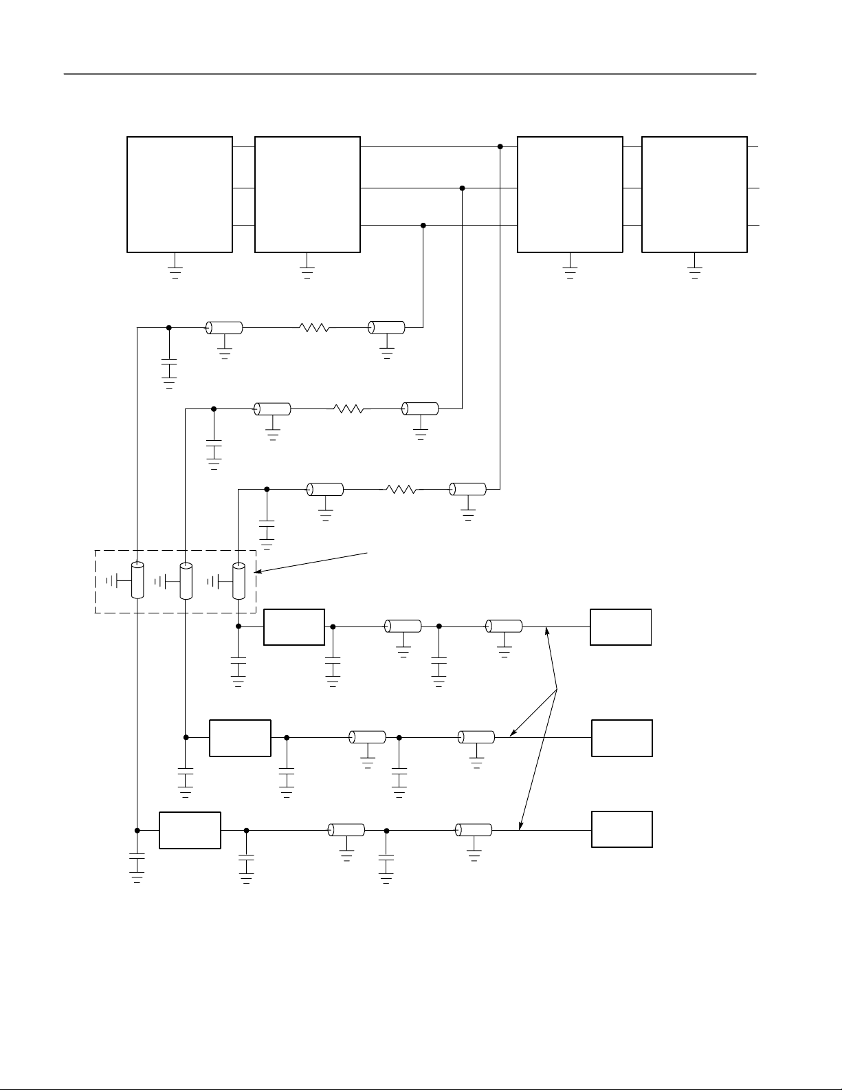
Specifications
LGA771/775 and PGA604
Socket microprocessor
Signal 1
Signal 2
Signal 3
VSS
75 Ω
~1300 mils
213 ps
C1
0.7 pF
~1300 mils
C2
0.7 pF
LGA771/775 and
PGA604 Socket
In 1
LGA socket
In 2
VSS
R1
200 Ω±15%
75 Ω
213 ps
~1300 mils
213 ps
Out 1
Out 2
Out 3In 3
R2
200 Ω±15%
75 Ω
75 Ω
~25 mils
4.6 ps
75 Ω
~25 mils
4.6 ps
R3
200 Ω±15%
75 Ω
~25 mils
4.6 ps
Probe head FR4
(see details below)
Node 7
Node 6
Node 3
Probe FR4
Node 2
Node 4Node 8
VSS
LGA771/775 Spacer
(see details below)
Node 8
LGA Spacer
Node 7
Node 2
Node 1
Node 3Node 9
VSS
C6
0.7 pF
Mated
Samtec
C5
0.7 pF
Mated
Samtec
C4
0.7 pF
C9
0.7 pF
C3
0.7 pF
Mated
Samtec
C8
0.7 pF
C7
0.7 pF
4.18 ns
75 Ω
~44’’
4.18 ns
75 Ω
~44’’
75 Ω
Coax Ribbon Loss
4”
--0.4dB@1.7GHz
477 ps
75 Ω
~44’’
4.18 ns
C11
0.4 pF
C12
0.7 pF
~1350 mils
C10
0.4 pF
75 Ω
~1350 mils
213 ps
75 Ω
~1300 mils
213 ps
75 Ω
213 ps
Receiver
Coax Ribbon Loss
--0.58dB@1.7GHz
Receiver
Receiver
Figure 8: Electrical load model for typical signals
32
TMSST2 LGA771, 775, and PGA604 Socket Hardware Support
Page 45

Dimensions
Figure 9 shows the dimensions of the TMSDPH2 probe head.
NOTE. For the TMSSPH1 probe head dimensions, refer to the product documentation.
64.33 mm
(2.533 in)
35.33 mm
(1.391 in)
16.86 mm
(0.664 in)
Specifications
73.66 mm
(2.900 in)
Center of processor
Socket pin 1
1.88 mm
(0.074 in)
11.55 mm
(0.455 in)
Figure 9: Dimensions of the probe head
4.57 mm
(0.180 in)
15.24 mm
(0.630 in)
40.36 mm
(1.589 in)
1.88 mm
(0.074 in)
17.20 mm
(0.677 in)
1.625 mm
(0.064 in)
TMSST2 LGA771, 775, and PGA604 Socket Hardware Support
33
Page 46

Specifications
Figure 10 shows the dimensions of the preprocessor unit.
CAUTION.
T o prevent damage to the circuitry in the prepr ocessor unit, you must observe the required
clearances in T able 7 on page 7 (clearances are not shown in Figure 10) .
474.32 mm
(18.674 in)
425.45 mm
(16.750 in)
420.37 mm
(16.550 in)
139.70 mm
(5.500 in)
Figure 10: Dimensions of the preprocessor unit
160.27 mm
(6.310 in)
34
TMSST2 LGA771, 775, and PGA604 Socket Hardware Support
Page 47

Design Review Checklists
Table 16: General checklist
Yes No NA Item
Have you contacted Tektronix
for any updates to the design
information in this Ref erence
section?
Table 17: Electrical checklist
Yes No NA Item
Have you performed electrical
simulations with the probe
adapter load models
Specifications
1
?
Will the target system operate
with the additional probe adapt-
1
er load
?
Are the electrical requirements
described in this Reference
section satisfied?
If the target system uses multiple reference voltages, does the
composite time and voltage eye
meet the electrical requirements
described in this Reference
section? See Figure 2 on
page 23.
1 See page 31 in the Specifi cati on section.
Table 18: Mechanical checklist
Yes No NA Item
Have you performed mechanical fit checks using the KOV
ProE model
1
The detailed mechanical keep-out-volume (KOV) for the probe head is described using the ProE 3D modeling package.
System designers should import the probe head KOV model into their modeling environment to ensure that the probe
head can be placed in the platform without any interference. Contact your Tektronix sales representative to obtain the
latest ProE probe head KOV model.
1
?
TMSST2 LGA771, 775, and PGA604 Socket Hardware Support
35
Page 48

Specifications
36
TMSST2 LGA771, 775, and PGA604 Socket Hardware Support
Page 49

Index
Index
A
Address bus, 18
Airflow clearance, preprocessor, 7
Application, logic analyzer configuration,
1
AVERAGE GTLREF jumpers, 5
C
Care and maintenance, external, 19
Circuit description, 15
Connections
P6860, 1
TMSCAB1 cable, 17
to target system, 9, 10
LGA771 heat sink kit, installation, 11
LGA775 heat sink kit, installation, 10
D
Data bus, 18
Dimensions
preprocessor unit, 34
probe head, 33
Disabling the cache, 18
Disassembler, logic analyzer configura-
tion, 1
J
Jumpers
AVERAGE GTLREF jumpers, 5
F2 ACQUIRED SIGNAL , 7
LGA771/LGA775, 6
OFFSET jumpers, 5
K
KOV, ProE model, 35
L
Loading diagrams, 31
Logic analyzer
compatibility, 14
configuration for disassembler, 1
configuration for the application, 1
M
Manual terms, vii
Modules connections, 17
O
OFFSET jumpers, 5
Optional accessory, 16
R
Reference, circuit description, 15
Removing hardware, from target
system, 12
Replaceable parts list, 13
Reset, 18
Restrictions
address bus, 18
data bus, 18
S
Shipping, probe adapter, assembled, 22
Socket F, basic configuration, 8
Specifications
AC input, 29
airflow clearance, 7
BCLK, 25
design review checklists, 35
DSTB strobe signal, 26
electrical, 23
environmental, 29
GTLREF voltage, 24
latched signal, 28
mechanical (dimensions), 33, 34
ProE model KOV, 35
Standard accessory, 16
Support package setups, 14
E
Electrical specifications, 23
AC adapter table, 29
AC/DC Signaling, 25
latched signals, 27
reference voltage, 23
strobe signals, 26
Environmental specifications, 29
electrostatic immunity, 29
temperature, 29
G
GTLREF jumpers, 5
I
Installing support software, 14
P
P6860, 1
Ports, XTGIP and Test, 7
Power, applying, 12
Probe adapter
configuring, 3
GTLREF jumpers, 5
hardware description, 1
jumper positions, 3
offset adjustments, 3
termination and reference
voltages, 6
voltage connections, 3
Probe configuration, 2
T
Termination and reference voltages, 6
TLA7AX4, probes, measurements, 1
TLA7AX4 module, measurements, 17
TMSCAB1 cable
configuration, 2
connections, 2, 17
TMSCAB1 Labels, 17
TMSDPH2 installation, to target
system, 8
TMSSPH1 installation, to target
system, 8
W
Weight, 29
TMSST2 LGA771, 775, and PGA604 Socket Hardware Support
37
Page 50

Index
38
TMSST2 LGA771, 775, and PGA604 Socket Hardware Support
 Loading...