

Page 1

xx
TLA5000 Series Logic Analyzer
ZZZ
Product Specifications & Performance Verification
Technical Reference
This document applies to TLA System Software Version
5.1SP1 and above
Warning
These servicing instructions are for use by qualified personnel
only. To avoid personal injury, do not perform any servicing
unless you are qualified to do so. Refer to all safety summaries
prior to performing service.
www.tektronix.com
071-2502-00
Page 2

Copyright © Tektronix. All rights reserved. Licensed software products are owned by Tektronix or its subsidiaries
or suppliers, and are protected by national copyright laws and international treaty provisions.
Tektronix products are covered by U.S. and foreign patents, issued and pending. Information in this publication
supersedes that in all previously published material. Specifications and price change privileges reserved.
TEKTRONIX and TEK are registered trademarks of Tektronix, Inc.
MagniVu and iView are registered trademarks of Tektronix, Inc.
Contacting Tektronix
Tektronix, Inc.
14200 SW Karl Braun Drive
P.O . Bo x 50 0
Beaverton, OR 97077
USA
For product information, sales, service, and technical support:
In North America, call 1-800-833-9200.
World wi de, vi s it www.tektronix.com to find contacts in your area.
Page 3

Warranty 2
Tektronix warrants that this product will be free from defects in materials and workmanship for a period of one (1)
year from the date of shipment. If any such product proves defective during this warranty period, Tektronix, at its
option, either will repair the defective product without charge for parts and labor, or will provide a replacement
in exchange for the defective product. Parts, modules and replacement products used by Tektronix for warranty
work may be ne
the property of Tektronix.
w or reconditioned to like new performance. All replaced parts, modules and products become
In order to o
the warranty period and make suitable a rrangements for the performance of service. Customer shall be responsible
for packaging and shipping the defective product to the service center designated by Tektronix, with shipping
charges prepaid. Tektronix shall pay for the return of the product to Customer if the shipment is to a location within
the country in which the Tektronix service center is located. Customer shall be responsible for paying all shipping
charges, duties, taxes, and any other charges for products returned to any other locations.
This warranty shall not apply to any defect, failure or damage caused by improper use or improper or inadequate
maintenance and care. Tektronix shall not be obligated to furnish service under this warranty a) to repair damage
resulti
b) to repair damage resulting from improper use or connection to incompatible equipment; c) to repair any damage
or malfunction caused by the use of non-Tektronix supplies; or d) to service a product that has been modified or
integrated with other products when the effect of such modification or integration increases the time or difficulty
of servicing the product.
THIS WARRANTY IS GIVEN BY TEKTRONIX WITH RESPECT TO THE PRODUCT IN LIEU OF ANY
OTHER WARRANTIES, EXPRESS OR IMPLIED. TEKTRONIX AND ITS VENDORS DISCLAIM ANY
IMPLIED WARRANTIES OF MERCHANTABILITY OR FITNESS FOR A PARTICULAR PURPOSE.
TEKTR
AND EXCLUSIVE REMEDY PROVIDED TO THE CUSTOMER FOR BREACH OF THIS WARRANTY.
TEKTRONIX AND ITS VENDORS WILL NOT BE LIABLE FOR ANY INDIRECT, SPECIAL, INCIDENTAL,
OR CONSEQUENTIAL DAMAGES IRRESPECTIVE OF WHETHER TEKTRONIX OR THE VENDOR HAS
ADVANCE NOTICE OF THE POSSIBILITY OF SUCH DAMAGES.
btain service under this warranty, Customer must notify Tektronix of the defect before the expiration of
ng from attempts by personnel other than Tektronix representatives to install, repair or service the product;
ONIX’ RESPONSIBILITY TO REPAIR OR REPLACE DEFECTIVE PRODUCTS IS THE SOLE
Page 4

Page 5

Table of Contents
General Safety Summary ......................................................................................... iv
Service Safety Summary........................ ................................ ................................ .. vi
Environmental Considerations .................................................................................. vii
Preface .............................................................................................................. ix
Related Documentation ...................................................................................... ix
Certifications and Compliances ................ ................................ ................................ ... 1
Specifications .................. ................................ .................................. ................... 4
External Oscilloscope (iView) Characteristics ................... ................................ .............. 19
Performance Ve rification Procedures............................................................................ 21
Summary Veri
Certification ..................... .................................. ................................ ............ 21
Test Equipment................................................................................................ 22
Functional Verification..... ................................ .................................. ................ 23
Performance Verification......................... .................................. .......................... 25
Checking the 10 MHz System Clock (CLK10) ........... ................................ ................ 26
Threshold Ac
Setup and Hold.......... .................................. ................................ .................... 30
Test Fixtures............................ .................................. ................................ .......... 34
Threshold Accuracy Test Fixture ........................................................................... 34
Setup and Hold Test Fixture............. ................................ ................................ .... 35
Calibration Data Report........................... ................................ ................................ 37
TLA5000 Ser
Test Data ....................................................................................................... 37
fication ........................................................................................ 21
curacy .............. ................................ .................................. .......... 27
ies......................................... ................................ ...................... 37
TLA5000 Series Product Specifications & Performance Verification i
Page 6

Table of Contents
List of Figure
Figure 1: Dimensions of the TLA5000 series logic analyzer............. .................................. .. 18
Figure 2: Defi
Figure 3: Setting trigger parameters. ... . ... ... . ... ... . .. . ... .... ... . .. . ... ... . ... ... . ... ... . ... ... . ... ... . ... ... 28
Figure 4: Set the trigger states ......................... .................................. ........................ 32
Figure 5: Threshold Accuracy test fixture ...................................................................... 34
Figure 6: Solder square pins to the SMA connector..................................... ...................... 35
Figure 7: Solder the SMA connectors together ............................ .................................. .. 36
Figure 8: Com
ning group parameters............................................................................ 27
pleted fixture with termination and coupler ........... ................................ ........ 36
s
ii TLA5000 Series Product Specifications & Performance Verification
Page 7

List of Tables
Table i: Related Documentation ..... .................................. ................................ .......... ix
Table 1: Atmo
Table 2: TLA5000 input parameters with probes .................... ................................ ........... 5
Table 3: TLA5000 timing latencies .............................................................................. 5
Table 4: TLA5000 external signal interface.......................... ................................ ........... 6
Table 5: TLA5000 channel width and depth .................................................................... 7
Table 6: Reference clock (CLK10) ...................... ................................ ......................... 8
Table 7: TLA5
Table 8: TLA5000 trigger system ............................................................................... 11
Table 9: TLA5000 MagniVu feature ............................................................................ 13
Table 10: TLA5000 Data Placement ............................................................................ 13
Table 11: TLA5000 Data handling .............................................................................. 14
Table 12: TLA5000B internal controller........................................................................ 14
Table 13: TLA
Table 14: TLA5000 display system ........... .................................. ................................ 15
Table 15: TLA5000 front-panel interface....................................................................... 16
Table 16: TLA5000 rear-panel interface........ ................................ ................................ 16
Table 17: TLA5000 AC power source ...... .................................. ................................ .. 17
Table 18: TLA5000 cooling...................................................................................... 17
Table 19: TL
Table 20: External oscilloscope (Integrated View or iView) characteristics ... ... . ... .... ... . .. . ... . ... ... . 19
Table 21: TDS1000, TDS1000B, TDS2000, and TDS2000B Series oscilloscope waveform edge
alignment ...................................................................................................... 20
Table 22: Test equipment ....................... ................................ .................................. 22
Table 23: Functional verification procedures................. .................................. ................ 23
Table 24: P
spheric characteristics............................................................................. 4
000 clocking ....................................................................................... 9
5000 internal controller.......................................................................... 15
A5000 mechanical characteristics................................................................ 17
arameters checked by verification procedures .................................................... 25
Table of Contents
TLA5000 Series Product Specifications & Performance Verification iii
Page 8

General Safety Summary
General Safet
To Avoid Fire or Personal
Injury
ySummary
Review the fol
this product or any products connected to it.
To avoid potential hazards, use this product only as specified.
Only qualified personnel should perform service procedures.
While using this product, you may need to access other parts of a larger system.
Read the safety sections of the other component manuals for warnings and
cautions related to operating the system.
Use Proper Power Cord. Use only the power cord specified for this product and
certified for the country of use.
Connect and Disconnect Properly. Do not connect or disconnect probes or test
leads while they are connected to a voltage source.
Ground the Product. This product is grounded through the grounding conductor
of the power cord. To avoid electric shock, the grounding conductor must be
connected to earth g
terminals of the product, ensure that the product is properly grounded.
lowing safety precautions to avoid injury and prevent damage to
round. Before making connections to the input or output
Observe All Terminal Ratings. To avoid fire or shock hazard, observe all ratings
and markings on the product. Consult the product manual for further ratings
information before making connections to the product.
The inputs are not rated for connection to mains or Category II, III, or IV circuits.
Power Disconnect. The power cord disconnects the product from the power source.
Donotblockthepowercord;itmustremain accessible to the user at all times.
Do Not Operate Without Covers. Do not operate this product with covers or panels
removed.
Do Not Operate With Suspected Failures. If you suspect that there i s damage to this
product, have it inspected by qualified s ervice personnel.
Avoid Exposed Circuitry. Do not touch exposed connections and components
when power is present.
Use Proper Fuse. Useonlythefusetypeandratingspecified for this product.
Do Not Operate in Wet/Damp Conditions.
Do Not Operate in an Explosive Atmosphere.
Keep Product Surfaces Clean and Dry.
Provide Proper Ventilation. Refer to the manual’s installation instructions for
details on installing the product so it has proper ventilation.
iv TLA5000 Series Product Specifications & Performance Verification
Page 9
General Safety Summary
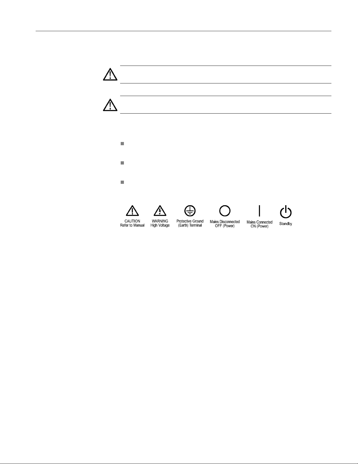
Terms in this Manual
Symbols and Terms on the
Product
These terms may
WAR N ING. Warning statements identify conditions or practices that could result
in injury or loss of life.
CAUTION. Caution statements identify conditions or practices that could result in
damage to this product or other property.
These terms may appear on the product:
DANGER ind
the marking.
WAR NI NG i
read the marking.
CAUTION i
The following symbol(s) may appear on the product:
appear in this manual:
icates an injury hazard immediately accessible as you read
ndicates an injury hazard not immediately accessible as you
ndicates a hazard to p roperty including the product.
TLA5000 Series Product Specifications & Performance Verification v
Page 10

Service Safety Summary
Service Safet
y Summary
Only qualified
Safety Summary and the General Safety Summary before performing any service
procedures.
Do Not Service Alone. Do not perform internal service or adjustments of this
product unless another person capable of rendering first aid and resuscitation is
present.
Disconnect Power. To avoid electric shock, switch off the instrument power, then
disconnect the power cord from the mains power.
Use Care When Servicing With Power On. Dangerous voltages or currents may
exist in t
disconnect test leads before removing protective panels, soldering, or replacing
components.
To avoid electric shock, do not touch exposed connections.
his product. Disconnect power, remove battery (if applicable), and
personnel should perform service procedures. Read this Service
vi TLA5000 Series Product Specifications & Performance Verification
Page 11

Environmental Considerations
This section provides information about the environmental impact of the product.
Product End-of-Life
iction of Hazardous
Restr
Handling
Substances
Observe the following guidelines when recycling an instrument or component:
Equipment Recycling. Production of this equipment required the extraction and
use of natural resources. The equipment may contain substances that could be
harmful to t
end of life. In order to avoid release of such substances into the environment and
to reduce the use of natural resources, we encourage you to recycle this product
in an appropriate system that will ensure that most of the materials are reused or
recycled appropriately.
Mercury Notification. This product uses an LCD backlight lamp that contains
mercury. Disposal may be regulated due to environmental considerations.
Please contact your local authorities or, within the United States, the Electronics
Industries Alliance (www.eiae.org) for disposal or recycling information.
This product has been classified as Monitoring and Control equipment, and is
outside the scope of the 2002/95/EC RoHS Directive.
he environment or human health if improperly handled at the product’s
This symb
requirements according to Directive 2002/96/EC on waste electrical and
electronic equipment (WEEE). For information about recycling options, check
the Supp
ol indicates that this product complies with the European Union’s
ort/Service section of the Tektronix Web site (ww w.tektronix.com).
TLA5000 Series Product Specifications & Performance Verification vii
Page 12

Environmental Considerations
viii TLA5000 Series Product Specifications & Performance Verification
Page 13
Preface
Related Documentation
This document lists the characteristics and specifications of the TLA5000 and
TLA5000B series logic analyzers. It also includes the performance verification
procedures.
otherwise noted. Microprocessor-related products and individual logic analyzer
probes have their own documentation for characteristics and specifications.
To prevent personal injury or damage consider the following requirements before
attempting service:
The procedures in this manual should be performed only by qualified service
personnel.
Read the General Safety Summary and Service Safety Summary found at
the beginning of this manual.
Be sure to follow all warnings, cautions, and notes in this manual.
The following table lists related documentation available for your logic analyzer.
The documentation is available on the TLA Documentation CD included with
your logic analyzer, and on the Tektronix Web site (www.Tektronix.com).
All references to TLA5000 also apply to TLA5000B, unless
To obtain documentation not specified in the table, contact your local Tektronix
representative.
Table i: Related Documentation
Item Purpose Location
TLA Quick Start User Manual
Online Help
Installation Quick Reference Cards Basic installation information
Installation Manuals
XYZs of
TLA Product Speci fications Specifications for other TLA products
Logic Analyzers
Basic operational overview
In depth operation and UI help
Detailed first-time installation information
Introduction to logic analyzer basics
TLA5000 Series Product Specifications & Performance Verification ix
Page 14
Preface
Table i: Related Documentation (cont.)
Item Purpose Location
TPI.NET Documentation
Detailed information for controlling the
logic analyzer u sing .NET
Field upgrade kits
Optional Service Manuals Self-service documentation for modules
TLA Application Software Release N otes Software description, compatibility,
Upgrade information for your logic
analyzer pro
and mainframes
impactofch
installation, upgrade, and operational
notes, and known issues.
duct
anges, contact information,
Go to Start→All Programs→Tektronix
logic Analyzer→TLA Release Notes
x TLA5000 Series Product Specifications & Performance Verification
Page 15

Certifications and Compliances
The certifications and compliances apply to all components of the Tektronix Logic
Analyzer family unless otherwise noted.
Certifications and Compliances
EC Declaration of
Conformity – EMC
Meets intent of Directive 2004/108/EEC for Electromagnetic Compatibility.
Compliance was demonstrated to the following specifications as listed in the
Official Journal of the European Communities:
EN 61326:1997. EMC requirements for Class A electrical equipment for
measurement, control, and laboratory use. Annex D.
IEC 61000-4-2:1999. Electrostatic discharge immunity
IEC 61000-4-3:2002. RF electromagnetic field immunity
IEC 61000-4-4:2004. Electrical fast transient/burst immunity
IEC 61000-4-5:2005. Power line surge immunity
IEC 61000-4-6:2003. Conducted RF immunity
IEC 61000-4-11:2004. Voltage dips and interruptions immunity
EN 61000-3-2:2000. AC power
EN 61000-3-3:1995. Voltage changes, fluctuations, and flicker
European Contact.
Tektronix UK, Ltd.
Western Peninsula
Western Road
Bracknell, RG12 1RF
United Kingdom
line harmonic emissions
Australia / New Zealand
Declaration of
Conformity – EMC
EC Declaration of
Conformity – Low Voltage
TLA5000 Series Product Specifications & Performance Verification 1
Complies with the EMC provision of the Radiocommunications Act per the
following standard, in accordance with ACMA:
EN 61326:1997. EMC requirements for electrical equipment for
measurement, control, and laboratory use.
Compliance was demonstrated to the following specification as listed in the
Official Journal of the European Communities:
Low Voltage Directive2006/96/EC.
EN 61010-1: 2001. Safety requirements for electrical equipment for
measurement control and laboratory use.
Page 16

Certifications and Compliances
U.S. Nationally Recognized
Testing Laboratory Listing
UL 61010B-1: 20
test equipment.
04, 2
nd
Edition. Standard for electrical measuring and
Canadian Certification
Additional Compliances
Equipment
Type
Safety Class
Pollution Degree
Descript
ion
CAN/CSA C22.2 No. 61010-1:2004. Safety requirements for electrical
equipment fo
IEC 61010-1: 2001. Safety requirements for electrical equipment for
measurement, control, and laboratory use.
Test and measuring equipment.
Class 1 – grounded product.
A measure of the contaminants that could occur in the environment around
and withi
considered to be the same as the external. Products should be used only in the
environment for which they are rated.
n a product. Typically the internal environment inside a product is
Pollution Degree 1. No pollution or only dry, nonconductive pollution occurs.
Products in this category are generally encapsulated, hermetically sealed, or
located in clean rooms.
Pollution Degree 2. Normally only dry, nonconductive pollution occurs.
Occasionally a temporary conductivity that i s caused by condensation must
be expected. This location is a typical office/home environment. Temporary
condensation occurs only when the product is out of service.
r measurement, control, and laboratory use. Part 1.
Pollution Degree 3. Conductive pollution, or dry, nonconductive pollution
that becomes conductive due to condensation. These are sheltered locations
e neither temperature nor humidity is controlled. The area is protected
wher
from direct sunshine, rain, or direct wind.
lution Degree 4. Pollution that generates persistent conductivity through
Pol
conductive dust, rain, or snow. Typical outdoor locations.
Pollution Degree
2 TLA5000 Series Product Specifications & Performance Verification
Pollution Degree 2 (as defined in IEC 61010-1). Note: Rated for indoor use only.
Page 17

Certifications and Compliances
Installation (Overvoltage)
Category Descriptions
Overvoltage Category
Termina l s on th
designations. The installation categories are:
Measurement C
low-voltage installation.
Measurement
installation.
Measurement
connected to the low-voltage installation.
Measuremen
directly connected to MAINS.
Overvoltage Category II (as defined in IEC 61010-1)
is product may have different installation (overvoltage) category
ategory IV. For measurements performed at the source of
Category III. For measurements performed in the building
Category II. For measurements performed on circuits directly
t Category I. For measurements performed on circuits not
TLA5000 Series Product Specifications & Performance Verification 3
Page 18

Specifications
Specification
s
The following
tables list the specifications for the TLA5000B and TLA5000 series
logic analyzers. All references to TLA5000 also apply to TLA5000B, unless
otherwise noted. All specifications are guaranteed unless noted Typical .Typical
characteristics describe typical or average performance and provide useful
reference information.
Specifications that are marked with the
symbol are checked directly (or
indirectly) in the Performance Verification chapter of this document.
The performance limits in this specification are valid with these conditions:
The instrument must be in an environment with temperature, altitude,
humidity, and vibration within the operating limits described in these
specifications.
The instrument must have had a warm-up period of at least 30 minutes.
The instrument must have been calibrated/adjusted at an ambient temperature
between +20 °C and +30 °C.
For optimum performance using an external oscilloscope, please consult the
documentation for any external o scillosc opes used with your Tektronix logic
analyzer to determine the warm-up period and signal-path compensation
requirements.
Table 1
Characteristic Description
Temper
Relative humidity
Alti
: Atmospheric characteristics
ature
tude
Operating (no media in CD or DVD drive)
+5 °C to +50 °C, 15 °C/hr maximum gradient, noncondensing (derated 1 °C per 305 m (1000 ft)
above 1524 m (5000 ft) altitude)
Nonoperating (no media in drive)
-20 °C to +60 °C, 15 °C/hr maximum gradient, noncondensing
Operating (no media in drive)
20% to 80% relative humidity, noncondensing. Maximum wet bulb temperature: +29 °C (derates
rela
Nono
8% to
humidity to approximately 22% at +50 °C).
Operating
To 3000 m (9843 ft), (derated 1 °C per 305 m (1000 ft) above 1524 m (5000 ft) altitude.
Nono
12,
tive humidity to approximately 22% at +50 °C).
perating (no media in drive)
80% relative humidity, noncondensing. Maximum wet bulb temperature: +29 °C (derates relative
perating
190 m (40,000 ft )
4 TLA5000 Series Product Specifications & Performance Verification
Page 19

Specifications
Table 2: TLA500
0 input parameters with probes
Characteristic Description
Threshold Accuracy
Threshold range and step size
±100 mV
Settable from +4.5 V to -2 V in 5 mV steps
Threshold channel selection 16 threshold g roups assigned to channels. P6410, P6417, P6418, and
P6419 probes have two threshold settings, one for the clock/qualifier
channel and one for the data channels. P6434 probes have four threshold
settings, one for each of the clock/qualifier channels and two for the data
channels (one per 16 data channels).
Channel-to-channel skew
Channel-to-channel skew (Typical)
Sample uncertainty
≤ ±150 ps maximum
≤ ±75 ps
Asynchronous
Sample period
Synchronous
125 ps
Input voltage range –2.5 to +5 V
Probe input resistance (Typical) 20 kΩ
Probe input c
(Typical)
apacitance
P6410, P6417
P6418 1.4 pF data channels
, P 6434
2pF
2 pF CLK/Qual
channels
P6419 < 0.7 pF
Minimum slew rate (Typical) 0.2 V/ns
Maximum operating signal 6.0 V
Probe overdr
ive
P6410, P6417
, P6418,
P6419
P6434
p-p
±250 mV or ±25% of signal swing minimum required beyond threshold,
whichever is greater
±300 mV or ±25% of signal swing minimum required beyond threshold,
whichever i
s greater
±4 V maximum beyond threshold
Maximum non
Minimum inp
(Typical)
Delay time from probe tip to module input probe
destructive input signal to probe
ut pulse width signal (single channel)
±15 V
1.5 ns (P643
4)
1.25 ns (P6410, P6417, P6418, P6419)
7.33 ns ±100
ps
connector (Typical)
Table 3: TLA5000 timing latencies
Characteristic Description
System Trigger and
External Signal Input
Latencies
1
(Typical)
External System Trigger Input to LA Probe Tip
2
External Signal Input to LA Probe Tip via Signal 3, 4 –656 ns + Clk
External Signal Input to LA Probe Tip via Signal 1, 2
4
–656 ns
–656 ns + Clk
3
3
TLA5000 Series Product Specifications & Performance Verification 5
Page 20

Specifications
Table 3: TLA5000 timing latencies (cont.)
Characteristic Description
System Trigger and
External Signal Output
Latencies (Typical)
1
All system trigger and external signal input latencies are measured from a falling-edge transition (active true low) with signals measured in the wired-OR
configuration.
2
In the Waveform window, triggers are always marked immediately except when delayed to the first sample. In the Listing window, triggers are always
marked on the next sample period following their occurrence.
3
CLK represents the time to the next master clock at the destination. In Normal clocking, this represents the delta time to the next sample clock. In External
clocking, this represents the time to the next master clock generated by the setup of the clocking state machine and the supplied SUT clocks and qualification date.
4
Signals 1 and 2 (ECLTRG 0, 1) are limited to a "broadcast" mode of operation, where only one source is allowed to drive the signal node at any one time.
That single source can be used to drive any combination of destinations.
5
SMPL represents the time from the event to the next valid data sample at the probe tip input. In the Normal Internal clock mode, this represents the delta time to
the next sample clock. In the MagniVu Internal clock mode, this represents 125 ps. In the External clock mode, this represents the time to the next masterclock
generated by the setup of the clocking state machine, the SUT-supplied clocks, and the qualification data.
6
All signal output latencies are validated to the rising edge of an active (true) high output.
LA Probe Tip to External System Trigger Out
LA Probe Tip to External
Signal Out via Signal 3,
56
4
LA Probe Tip to External
Signal Out via Signal 1, 2
456
OR function 772 ns + SMPL
AND function 772 ns + SMPL
normal function 772 ns + SMPL
inverted logic on backplane
56
778 ns + SMPL
774 ns + SMPL
Table 4: TLA5000 external signal interface
Characteristic Description
System trigger input
External signal input
Input destination
Input levels
V
IH
V
IL
Input mode
Minimum pulse width 12 ns
Active period Accepts system triggers during valid acquisition periods via real-time
Maximum input voltage 0 to +5 V peak
Input destination
Input levels
V
IH
V
IL
Input mode
Input bandwidth
1
Active period Accepts signals during valid acquisition periods via real-time gating.
Maximum input voltage 0 to +5 V peak
TTL compatible input via rear panel mounted BNC connectors
System trigger
TTL compatible input
≥ 2.0 V
≤ 0.8 V
Falling edge sensitive, latched (active low)
gating, resets system trigger input latch between valid acquisition periods.
TTL compatible input via rear panel mounted BNC connectors
Signal 1, 2, 3, 4
TTL compatible input
≥ 2.0 V
≤ 0.8 V
Active (true) low, level sensitive
Signal 1, 2 Signal 3, 4
50 MHz square wave minimum 10 MHz square wave minimum
6 TLA5000 Series Product Specifications & Performance Verification
Page 21

Specifications
Table 4: TLA5000 external signal interface (cont.)
Characteristic Description
System trigger output
Source selection System trigger
Source mode Active (true) low, falling edge latched
Active period
Output levels
V
OH
V
OL
Output protection Short-circuit protected (to ground)
External signal output
Source selection Signal 1, 2, 3, 4, or 10 MHz clock
Output modes level
sensitive
Output levels
V
OH
V
OL
2
Active period
Output protection Short-circuit protected (to ground)
1
The input bandwidth specification only applies to signals to the External Signal input; it does not apply to signals applied to the External Signal input and sent
back to the External Signal output.
2
The output bandwidth specification only applies to signals to the External Signal output; it does not apply to signals applied to the External Signal output
and sent back to the External Signal input.
TTL compatible output via rear panel mounted BNC connectors
Outputs system trigger state during valid acquisition period, resets system
trigger output to false state between valid acquisitions
50 Ω back terminated TTL-compatible output
≥4 V into open circuit
≥ 2Vinto50Ω to ground
≤ 0.7 V sinking 10 mA
TTL compatible outputs via rear panel mounted BNC connectors
User definable active (true) low or active (true) high
50 Ω back terminated TTL output
≥4 V into open circuit
≥2Vinto50Ω to ground
≤ 0.7 V sinking 10 mA
Signal 1, 2 Signal 3, 4Output bandwidth
50 MHz square wave minimum 10 MHz square wave minimum
Outputs signals during valid acquisition periods, resets signals to false
state between valid acquisitions
Outputs 10 MHz clock continuously
Table 5: T
LA5000 channel width and depth
Characteristic Description
Product
TLA5201
TLA5202
TLA5203
TLA5204
ChannelsNumber of channels
32 data an
d2clock
64 data and 4 clock
96 data, 4 clock, and 2 qualifier
128 data,
4 c lock, and 4 qualifier
TLA5000 Series Product Specifications & Performance Verification 7
Page 22

Specifications
Table 5: TLA5000 channel width and depth (cont.)
Characteristic Description
Acquisition memory depth
Product Memory depth
TLA520XB 2 M or optionally 8 M or 32 M
TLA520X 512 K or optionally 2 or 8 M
1
PowerFlex op
tions
Table 6: Reference clock (CLK10)
Characteristic Description
Clock accuracy
10 MHz ±100 ppm
samples
samples
1
1
8 TLA5000 Series Product Specifications & Performance Verification
Page 23

Specifications
Table 7: TLA500
0 clocking
Characteristic Description
Asynchronous
Internal sampling period
clocking
1
500 ps to 50 ms i
store data when it has changed (transitional storage)
2 ns minimum for all channels
1nsminimumfo
0.5 ns minimum for quarter channels (using 4:1 demultiplex mode)
Minimum r ecognizable word2(across all channels)
Channel-to-channel skew + sample uncertainty
Example: for a 2 ns sample period and a P6419, or P6434 Probe = 400 ps
+ 2 ns = 2.4 ns
Synchronous c
Number of mas
locking
ter clock channels
3
Product
TLA5201
TLA5202
TLA5203
TLA5204
Number of qualifier channels
4
Product
TLA5201
TLA5202
TLA5203
TLA5204
Setup and hold w indow size
Setup and hold window size (Typical)
1 ns maximum, any clock to any single data or qualifier channel
1.5 ns, all channels
n a 1-2-5 sequence. Storage control can be used to only
r half channels (using 2:1 demultiplex mode)
Clock Channe
ls
2
4
4
4
Qualifier Channels
0
0
2
4
TLA5000 Series Product Specifications & Performance Verification 9
Page 24

Specifications
Table 7: TLA5000 clocking (cont.)
Characteristic Description
Setup and hold window range For each channel, the setup and hold window can be moved from +8.0 ns
(Ts) to -8.0 ns (Ts) in 0.125 ns steps. The hold time follows the setup time
by the setup and hold window size.
Maximum synchronous clock rate
2X Demux clocking
TLA5203, TLA5204
TLA5201, TLA5202
Time between Demultiplex clock edges (Typical) Same limitations as normal synchronous acquisition
4X Demux clocking
TLA5203, TLA5204
235 MHz in full speed mode (4.25 ns minimum between active clock
edges)
Any individual channel may be demulti plexed with its partner channel.
Channels demultiplex as follows:
A3(7:0) to/from
A2(7:0) to/from
A1(7:0) to/from
A0(7:0) to/from
C3(7:0) to/from
C2(7:0) to/from
E3(7:0) to/from
E2(7:0) to/from
CK3 to/from
CK2 to/from
CK1 to/from
CK0 to/from
Any individual channel may be demulti plexed with its partner channel.
Channels demultiplex as follows:
A3(7:0) to/from
A2(7:0) to/from
A1(7:0) to/from
A0(7:0) to/from
Unlike 2X demultiplexing, the channels within a group of four cannot
arbitrarily drive the others.
E3(7:0) to
A3(7:0) to
A1(7:0) to
C3(7:0) to
CK3 to
CK1 to
D3(7:0)
D2(7:0)
D1(7:0)
D0(7:0)
C1(7:0)
C0(7:0)
E1(7:0) (TLA5204 only)
E0(7:0) (TLA5204 only)
Q2 (TLA5204 only)
Q3 (TLA5204 only)
Q0
Q1
C3(7:0)
C2(7:0)
D1(7:0) (TLA5202 only)
D0(7:0)( TLA5202 only)
E2(7:0), E1(7:0), E0(7:0) (TLA5204 only)
A2(7:0), D3(7:0), D2(7:0)
A0(7:0), D1(7:0), D0(7:0)
C2(7:0), C1(7:0), C0(7:0)
CK2, Q3, Q2 (TLA5204 only)
CK0, Q1, Q0
10 TLA5000 Series Product Specifications & Performance Verification
Page 25

Specifications
Table 7: TLA5000 clocking (cont.)
2X Demux clocking
TLA5201, TLA5202
Unlike 2X demultiplexing, the channels within a group of four cannot
arbitrarily drive the others.
A1(7:0) to
C3(7:0) to
A0(7:0), D1(7:0), D0(7:0) TL:A5202 only
C2(7:0), A3(7:0), A2(7:0)
Time between Demultiplex clock edges (Typical) Same limitations as normal synchronous acquisition
Clocking state machine
Pipeline delays
Each channel can be programmed with a pipeline delay of 0 through 7
active clock edges.
1
It is possib
2
Applies to asynchronous clocking only. Setup and hold window specification applies to synchronous clocking only.
3
Any or all of the clock channels may be enabled. For an enabled clock channel, either the rising, falling, or both edges can be selected as the active clock
edges. The clock channels are stored.
4
All qualifier channels are stored. For custom clocking there are an additional 4 qualifier channels on C2 3:0 regardless of channel width.
le to use storage control and only store data when it has changed (transitional storage).
Table 8: TLA5000 trigger system
Characteristic Description
Triggering Resources
Word/Range recognizers
16 word recognizers. The word recognizers can be combined to form full width, double
bounded, range recognizers. The following selections are available:
16 word recognizers
13 word recognizers
10 word recognizers
7 word recognizers
4 word recognizers
Range recognizer channel order
From most-significant probe group to least-significant probe group: C3 C2 C1 C0 E3 E2 E1
E0 A3 A2 D3 D2 A1 A0 D1 D0 Q3 Q2 Q1 Q0 CK3 CK2 CK1 CK0
Missing channels for instruments with fewer than 136 channels are omitted.
Glitch detector
12
Channel groups can be enabled to detect glitches.
Glitches are subject to pulse width variations of up to ±125 ps
Minimum detectable glitch pulse
width (Typical)
Setup and hold violation detector
13
1.25 ns (single channel with P6434 probe)
1.0 ns (P6410, P6417, P6418, P6419 probe)
Any channel can be enabled to detect a setup or hold violation. The range is from 8.0 ns before
the clock edge to 8.0 ns after the clock edge in 0.125 ns steps. The channel setup and hold
violation size can be individually programmed.
The range can be shifted towards the positive region by 0 ns, 4 ns, or 8 ns. With a 0 ns shift, the
range is +8 ns to -8 ns; with a 4 ns shift, the range is +12 ns to -4 ns; with an 8 ns shift, the range
is +16 ns to 0 ns. The sample point selection region is the same as the setup and hold window.
Any setup value is subject to variation of up to the channel skew specification. Any hold value
is subject to variation of up to the channel skew specification.
0 range recognizers
1 range recognizer
2 range recognizers
3 range recognizers
4 range recognizers
TLA5000 Series Product Specifications & Performance Verification 11
Page 26

Specifications
Table 8: TLA5000 trigger system (cont.)
Characteristic Description
Transition detector
Counter/Timers 2 counter/timers, 51 bits wide, can be clocked up to 500 MHz.
External Signal In
External Trigger In A backplane input signal that causes both the main acquisition and the MagniVu acquisition
Active trigger resources
Trigger States
Trigger State sequence rate
Trigger Mac
Main acquisition trigger Triggers the main acquisition memory.
Main trigger position
MagniVu™ acquisition trigger
MagniVu™ trigger position
Increment
& decrement counter
Reloadable word recognizer
Reloadable word recognizer
latency
Start/Stop timer Either of the two counter/timers used as timers can be s tarted or stopped.
Reset counter/timer Either of the two counter/timers can be reset.
Signal out
Trigger o
Storage C
Global st
ut
ontrol
orage
1
1
hine Actions
16 transition detectors.
Any channel group can be enabled or disabled to detect a rising transition, a falling transition,
or both rising and falling transitions between the current valid data sample and the previous
valid data sample.
51
Maximum count is 2
Maximum time is 4.5 X 10
-1.
6
seconds or 52 days.
Counters and timers can be set, reset, or tested and have zero reset latency.
A backplane input signal.
to trigger if they are not already triggered.
16 maximum (excluding counter/timers)
Word recognizers are traded off one-by-one as External Signal In, glitch detection, setup and
hold detection, or transition detection resources are added.
16
Same rate as valid data samples received, 500 MHz maximum.
Trigger position is programmable to any data sample (2 ns boundaries).
Triggering of MagniV memory is controlled by the main acquisition trigger machine.
The MagniV trigger position is programmable within 2 ns boundaries and separate from the
main acquis
Either of t
Loads the c
ition memory trigger position.
he two counter/timers used as counters can be increased or decreased.
urrent acquired data sample into the reference value of the word recognizer via
a trigger machine action. All data channels are loaded into their respective word recognizer
reference register on a one-to-one manner.
378 ns
When a cou
nter/timer is used as a timer and is reset, the timer continues from the started or
stopped state that it was in prior to the reset.
A signal s
A trigger
Storage i
ent to the backplane to be used by other instruments.
out signal sent to the backplane to trigger other instruments.
s allowed only when a specific condition is met. This condition can use any of the
trigger machine resources except for the counter/timers. Storage commands definedinthe
current trigger state will override the global storage control.
Global s
torage can be used to start the acquisition with storage initially turned on (default) or
turned off.
12 TLA5000 Series Product Specifications & Performance Verification
Page 27

Specifications
Table 8: TLA5000 trigger system (cont.)
Characteristic Description
By event
Block storage
Glitch violation storage The acquisition memory can be enabled to store glitch violation information with each data
Setup and hold violation storage The acquisition memory can be enabled to store setup and hold violation information with each
1
Each use of
2
Any glitch is subject to pulse width variation of up to the channel-to-channel skew specifica tion + 0.25 ns.
3
Any setup value is subject to variation of up to the channel skew specification. Any hold value is subject to variation of the channel skew specifications.
External Signal In, glitch detector, setup and hold violation detector, or transition detector requires a trade-off of one word recognizer resource.
Storage can be turned on or off; only the current sample can be stored. The event storage
control overrides any global storage commands.
When enabled, 31 samples are stored before and after the valid sample.
Not allowed when glitch storage or setup and hold violation is enabled.
sample when asynchronous clocking is used. The probe data storage size is reduced by one
half (the other half holds the violation information). The fastest asynchronous clocking rate
is reduced to 4 ns.
data sample when synchronous clocking is used. The probe data storage size is reduced by
one half (the other half holds the violation information). The maximum clock rate in this mode is
235 MHz.
Table 9: TLA5000 MagniVu feature
Characteristic Description
MagniVu memory depth 16,000 samples per channel
MagniVu sampling period Data is asynchronously sampled and stored every 125 ps in a separate
high resolution memory. The storage speed may be changed (by software)
to 250 ps, 500 ps, or 1000 ps so that MagniVu memory covers more time
at a lower resolution.
Table 10: TLA5000 Data Placement
Charact
System t
Data cor
eristic
ime zero placement error (Typical)
relation error (Typical)
Descrip
±4 ns + backplane 10 MHz skew
All stor
±200 ps + system time zero placement error
tion
ed data is referenced to this point.
TLA5000 Series Product Specifications & Performance Verification 13
Page 28

Specifications
Table 10: TLA5000 Data Placement (cont.)
Characteristic Description
Relative timestamp accuracy (Typical)
Timestamp counter and resolution 125 ps resolution
±100 ps + sample uncertainty + backplane 10 MHz clock jitter and
tolerance
This specificationcanbeusedtoindicatetheaccuracyofatime
measurement between samples. When measuring between samples,
only the time difference between samples should be used to i ndicate
accuracy. For example, if one sample has a timestamp of one hour and
another sample has a timestamp of one hour and 10 ms, the 10 ms is
the period of time used to determine the amount of error caused by the
10 MHz clock tolerance.
3.25 days duration
Table 11: TLA5000 Data handling
Character
Nonvolati
istic
le memory retention time (Typical)
Descripti
Battery is
on
integral to the NVRAM. Battery life is > 10 years.
Table 12: TLA5000B internal controller
Characteristic Description
Operating system Microsoft Windows
Microprocessor
Main memory
Cache memory
Real-time clock and
CMOS setups NVRAM
Hard disk drive
Style 184 pin DDR2 SDRAM DIMM gold-plated
Speed 266 MHz DDR2 PC2100
Installed configuration
Maximum configuration 4 GB (four 1 GB DIMMs)
Capacity
Style
Intel Celeron, 2.93 GHz
512 MB
Level 2 (L2) Write-back cache
256 KB
Integrated
Real-time clock/calendar. Standard and advanced PC CMOS setups.
Battery life is typically > 3 years when the logic analyzer is not connected
to line voltage. When connected to line voltage the life of the battery is
extended. Lithium battery, CR2032
80 GB standard PC compatible IDE (Integrated Device Electronics) hard
disk drive residing on a serial ATA interface.
Continually subject to change due to the fast-moving PC component
environment. Storage capacities valid at product introduction.
14 TLA5000 Series Product Specifications & Performance Verification
Page 29

Table 12: TLA5000B internal controller (cont.)
Characteristic Description
CD-DVD drive Standard PC compatible IDE (Integrated Device Electronics)
CD-RW/DVD-R drive residing on an EIDE interface.
Continually subject to change due to the fast-moving PC component
environment.
Floppy disk drive
Standard 3.5 inch 1.44 MB PC compatible high-density, double-sided
floppy disk drive on the USB bus
Table 13: TLA5000 internal controller
Specifications
Character
Operating
Microprocessor
Main memory
Real-time clock and
CMOS setu
play NVRAM retention
time
Hard disk drive
CD-RW drive Standard PC compatible IDE (Integrated Device Electronics) CD-RW drive
Floppy disk drive
istic
system
ps, plug &
Descripti
Microsoft
Intel Cele
PC2100 DDR
Style 184 pin DI
Speed
Installe
dconfiguration
100 MHz
512 MB loaded in one socket
Battery l
to line voltage. When connected to line voltage the life of the battery is
extended. Lithium battery, CR2032
80 GB standard PC compatible IDE (Integrated Device Electronics) hard
disk dri
Continually subject to change due to the fast-moving PC component
environment. Storage capacities valid at product introduction.
residi
Continually subject to change due to the fast-moving PC component
environment.
Standard 3.5 inch 1.44 MB PC compatible high-density, double-sided
floppy d
on
Windows
ron, 2 GHz
SDRAM
MM, 2 Sockets
ife is typically > 3 years when the logic analyzer is not connected
ve residing on an EIDE interface.
ng on an EIDE interface.
isk drive.
Table 14: TLA5000 display system
Characteristic Description
Display memory
Display selection
8 MB SDRAM-onboard the ATI Mobility I video controller
Hardware sense of external SVGA monitor connected to the external primary display
connector prior to the BIOS boot sequence enables the operation of that display output.
The internal LCD display is enabled at all times. The internal LCD and the primary
external displays operate at the same resolution (limited to 1024 X 768 on current TFT
LCD) and display rates. Dynamic Display Configuration 1 (DDC1) support for the
external SVGA monitor is provided.
TLA5000 Series Product Specifications & Performance Verification 15
Page 30

Specifications
Table 14: TLA5000 display system (cont.)
Characteristic Description
Display modes
External display
drive
Internal D isplay
Primary display
size (RAGE M1
chip)
Secondary display
size (845GV chip)
Classification Thin Film Transistor (TFT) 10.4 inch active-matrix color LCD display; CCFL backlight;
Resolution 1024 x 768 pixels
Color Scale
Refresh rate
Three displays can be driven independently, the LCD display and two external displays.
The LCD display and one of the external displays are driven from the ATI RAGE Mobility
M1 chip and are the primary displays; the two displays are independent. A third display
is the second external display port driven from the motherboard (secondary display).
TwoVGa, SVGA, or XGA-compatible analog output ports.
Display size selected via Windows
Resolution (pixels) Colors Refresh rates
1024 x 768, 1280 x
1024, or 1600 x 1200
Resolution (pixels) Colors Refresh rates
640 x 480
800 x 600
1024 x 768
1280 x 1024
1600 x 1200
1920 x 1440
intensity controllable via software.
256K
60
256, 64 K , 16.8 M 60, 75, 85, 100
256, 64 K , 16.8 M
256, 64 K , 16.8 M
256, 64 K , 16.8 M
256, 64 K , 16.8 M
256, 64 K , 16.8 M
256, 64K
60, 75, 85
60, 75, 85
60, 75, 85
60, 75, 85
60, 75, 85
60, 75
Table 15: T
Characteristic Description
QWERTY ASCII to support naming of files, traces, and keyboard equivalents of
Special Function Knobs Various functions
LA5000 front-panel interface
pointing device inputs for menus.
Table 16: TLA5000 rear-panel interface
Characteristic Description
Parallel Interface Port (LPT) 25-pin sub-D Parallel Port Connector, Extended Parallel Port (EPP), or
Enhanced Capabilities Port (ECP)
Serial Interface Port (COM 1) 9-pin male sub-D connector to support RS-232 serial port
Two USB Ports Two USB 2.0 (Universal Serial Bus) compliant ports
SVGA Output Ports (SVGA OUT) 15-pin sub-D SVGA connectors (two each, one Primary, one Secondary)
16 TLA5000 Series Product Specifications & Performance Verification
Page 31

Table 16: TLA5000 rear-panel interface (cont.)
Characteristic Description
Mouse Port
Keyboard Port
PS/2 compatible mouse port utilizing a m ini DIN connector
PS/2 compatible keyboard port utilizing a mini DIN connector
Table 17: TLA5000 AC power source
Characteristic Description
Source Voltage and Frequency 100 V
Maximum Power Consumption
Steady-State Input Current
Inrush Surge Current
Power Factor Correction
240 Watts line power maximum
4A
65 A maximum
Yes
On/Standby Switch and Indicator Front Panel On/Standby switch, w ith indicator.
The power c
RMS
maximum
RMS
to 240 V
±10%,47Hzto63Hz
RMS
ord provides main power disconnect.
Specifications
Table 18: TLA5000 cooling
Characteristic Description
Cooling System Forced air circulation (negative pressurization) utilizing two fans operating
in parallel
Cooling Clearance 51 mm (2 in), sides and rear; unit should be operated on a flat,
unobstructed surface
Table 1
Characteristic Description
Overall Dimensions (See Figure 1.)
Weight
9: TLA5000 mechanical characteristics
Includes empty accessory pouch and front cover
01
TLA52
TLA5202
TLA5203
TLA520
11.8Kg(25lb15oz)
11.85Kg(26lb2oz)
11. 9 K
4
12Kg(26lb7oz)
g(26lb4oz)
TLA5000 Series Product Specifications & Performance Verification 17
Page 32

Specifications
Figure 1: Dimensions of the TLA5000 series logic a nalyzer
18 TLA5000 Series Product Specifications & Performance Verification
Page 33

External Oscilloscope (iView) Characteristics
External Osci
lloscope (iView) Characteristics
The following
table lists the characteristics for iView (Integrated View) and for
the Tektronix logic analyzer when connected to an external oscilloscope. For
detailed information on the individual specifications of the external oscilloscope,
refer to the documentation that accompanies the oscilloscope.
Table 20: External oscilloscope (Integrated View or iView) characteristics
Characteri
Supported T
TLA applica
Minimum recommended TLA controller RAM
Supported external oscilloscopes as of January, 2008
(For the lat
visit our Web site at www.tektronix.com.)
External oscilloscope software or firmware version
number
Maximum numb
iView cable length
stic
ektronix logic analyzer instruments
tion software version
1
est list of supported external oscilloscopes,
er of external oscilloscopes
5
Descriptio
TLA5000 and TLA5000B series
TLA7012, TL
V5.1SP1 or g
256 MB
TDS1000, TDS200023, T DS 1000B and TDS2000B Series
TDS3000 and
module required)
DPO4000 and MSO4000 Series
TDS5000 and
TDS6000, TDS6000B, and TDS6000C Series
DPO7000 and DPO7000B Series
DPO70000 an
TDS7000 and TDS7000B Series
CSA7000 and CSA7000B Series
TDS654C, TD
TDS754C, T DS784C, TDS724D, TDS754D, TDS784D, TDS794D
Product Version
TDS684C, TD
TDS3000 series
DPO4000 series
TDS5000 seri
TDS6000 series
DPO7000 series
TDS7000, CSA
One per Tektr
6.56 ft (2 m)
n
A7016
reater
TDS3000B Series (TDS3GM GPIB/RS-232 communication
TDS5000B Series
d DSA70000 series
S684C, TDS694C
S694C
es
7000 series
onix logic analyzer mainframe
34
4
Any version
Any version
Any version
Any version
Any version
Version 1.2 or greater
TLA5000 Series Product Specifications & Performance Verification 19
Page 34

External Oscilloscope (iView) Characteristics
Table 20: External oscilloscope (Integrated View or iView) characteristics (cont.)
Characteristic Description
Time correlation uncertainty6(Typical at system trigger)
1
If RAM is less than 256 MB, the record length of the external oscilloscope may be limited to 1 M.
2
An GPIB extender is needed to connect the iView cable to the oscilloscope. One end of a standard GPIB cable can be used.
3
If you encounter possible alignment problems with the logic analyzer and oscilloscope waveform edges, refer to Aligning Logic Analyzer and Oscilloscope
Waveform Edges. (See page 20, Aligning Logic Analyzer and Oscilloscope Waveform Edges.)
4
AGPIBtoUSBa
5
When used with a TLA7016 mainframe and an external PC (such as TLA7PC1), the instruments must be physically located close together so that the iView
cable can span both instruments. Removing the sleeving from the iView cable assembly increases the spacing distance available between the external
PC and the TLA7016 mainframe.
6
Includes sampling uncertainty, typical jitter, slot-to-slot skew, and probe-to-probe variations to provide a typical number for the measurement.
dapter (TEK-USB-488) is required to connect the iView cable to the oscilloscope.
3 ns Logic analyzer triggers external
oscilloscope
(2 ns + logic analyzer sample
period + external oscilloscope
sample period)
5ns
External oscilloscope triggers logic
analyzer
(4 ns + logic analyzer sample
period + external oscilloscope
sample period)
Aligning Logic Analyzer
and Oscilloscope
Waveform Edges
The first time that you take an acquisition after changing the horizontal scale
setting on TDS1000, TDS1000B, TDS2000, or TDS2000B series oscilloscopes,
the logic analyzer and oscilloscope waveform edges may not be aligned within
the listed specification. You can realign the waveform positions in the waveform
window tha
t contains the oscilloscope data (Menu bar > Data > Time Alignment).
Make sure that the external oscilloscope is the data source and then adjust the time
offset to align the waveforms. Use the following approximate offsets for various
horizontal scale settings. (See Table 21.)
Table 21: TDS1000, TDS1000B, TDS2000, and TDS2000B Series oscilloscope
waveform edge alignment
Horizontal scale Time offset
100 ns
250 ns –11 ns
500 ns –18 ns
1 μs –12 ns
2.5 μs –50 ns
5 μs
10 μs –250 ns
25 μs –650 ns
–5 ns
–120 ns
20 TLA5000 Series Product Specifications & Performance Verification
Page 35

Performance Verification Procedures
This chapter contains procedures for functional verification, certification, and
performance verification procedures for the TLA5000 and TLA5000B series logic
analyzer mai
year or following repairs that affect certification.
Summary Verification
Functional verification procedures verify the basic functionality of the instrument
inputs, outputs, and basic instrument actions. These procedures include power-on
diagnostics, extended diagnostics, and manual check procedures. These
procedures can be used for incoming inspection purposes.
Performance verification procedures confirm that a product meets or exceeds the
performance requirements for the published specifications documented in the
Specifications chapter of this manual. The performance verification procedures
certify t
standards.
nframes. Generally, you should perform these procedures once per
he accuracy of an instrument and provide a traceability path to national
Certi
fication
As you co
calibration data report to keep on file with your instrument. A blank copy of the
calibration data report is provided with this manual. The calibration data report is
intended to be copied and used to record the results of the calibration/certification
procedures.
The system clock of the controller is checked for accuracy, and the input probe
channels are checked for threshold accuracy and setup and hold accuracy. The
instr
performance verification procedures and record the certifiable parameters in a
copy of the Calibration Data Report at the end of this chapter.
mplete the performance verification procedures, you can fill out a
ument is certifiable if these parameters meet specifications. Complete the
TLA5000 Series Product Specifications & Performance Verification 21
Page 36

Performance Verification Procedures
Test Equipment
These procedures use external, traceable signal sources to directly test
characteristics that are designated as checked
this manual. Always warm up the equipment for 30 minutes before beginning
the procedures.
in the Specifications chapter of
Table 22: Tes
Item number a
description Minimum requirements Example
1. Logic analy
2. Logic analyzer probes
3. Frequency counter
4. Digital ti
generator
5. DC voltage source
(see footn
6. Digital multimeter with
probes
7. Cable, pr
50 Ω coaxial
8. Setup and Hold test
fixture
9. Threshold Accuracy
test fixture
1
Some timing generators (for example, the Tektronix DTG5274) include an internal DC voltage source that can be used instead of a separate power source.
2
Only needed to verify the output of the voltage source if the source does not meet specification. In this case, the DMM becomes the traceable instrument.
t equipment
nd
zer
ming
1
ote)
2
ecision
TLA5000 or T
General purpose Tektronix logic analyzer probes; one probe
required fo
Frequency
100 MHz
>235 MHz, ± 0.1% accuracy
DC output: 0–5 V, ± 0.1% accuracy
0–5 V, ± 0.1% accuracy Tektronix PS281
6.5 digit display, 35 ppm, 1 year accuracy, 1000 readings per
minute
50 Ω,36in
User-built (See page 34, Te st Fi xt u re s .)
User-built (See page 34, Te st Fi xt u re s .)
LA5000B series logic analyzer
r every 17 channels.
accuracy: <0.0025% Frequency range: 1 kHz to
, male-to-male BNC connectors
TLA5201, TL
TLA5202B, TLA5203, TLA5203B,
TLA5204, TLA5204B
P6410, P6417, or P6418
Agilent 33131A
Tektronix DTG5274
Fluke 8845
Tektronix part number 012-0482-XX
A501B, TLA5202,
A/8846A
22 TLA5000 Series Product Specifications & Performance Verification
Page 37

Performance Verification Procedures
Functional Ve
Power-on a
rification
nd Fan
Operation
The following table lists functional verification procedures for the benchtop and
portable mainframes. If necessary, refer to the TLA5000B Series Logic Analyzer
Installatio
Table 23: Functional verification procedures
Instrument Procedure
TLA5000 Series logic analyzers
Complete the following steps to check the power-on and fan operation of the
logic analyzer:
1. Power on the instrument and observe that the On/Standby switch illuminates.
2. Check that the fans spin without undue noise.
3. If there are no failures indicated, the power-on diagnostics pass when you
n Manual for installation instructions.
Power-on and fan operation
Power-up diagnostics
Extended diagnostics
CheckIt Utilities diagnostics
power on the mainframe(s).
TLA5000 Series Product Specifications & Performance Verification 23
Page 38

Performance Verification Procedures
Extended Diagnostics
Do the followin
NOTE. Running the extended diagnostics will invalidate any acquired data. If
you want to save any of the acquired data, do so before running the extended
diagnostics.
Prerequisites Warm-up time: 30 minutes
Perform the following tests to complete the functional verification procedure:
1. If you have not already done so, power on the instrument and start the logic
analyzer application if it did not start by itself.
2. Go to the System menu and select Calibration and Diagnostics.
3. Verify that all power-on diagnostics pass.
4. Click the Extended Diagnostics tab.
5. Select All
sheet.
All tests
status depending on the outcome of the tests.
g steps to run the extended diagnostics:
Modules, All Tests, and then click the Run button on the property
that displayed an "Unknown" status will change to a Pass or Fail
CheckIt Utilities
6. Scroll th
CheckIt Utilities is a comprehensive software application used to check and verify
the operation of the hardware in the instrument. To run the software, you must
have ei
NOTE. To check the DVD/CD drive, you must have a test disc installed before
starting the CheckIt CD-ROM test. The disc needs to contain a file with a size
between 5 MB and 15 MB.
To run CheckIt Utilities, follow these instructions:
1. Quit the logic analyzer application.
2. Click the Windows Start button.
3. Select All Programs → CheckIt Utilities.
4. Run the tests. If necessary, refer to the CheckIt Utilities online help for
information on running the software and the individual tests.
rough the tests and verify that all tests pass.
ther a keyboard, mouse, or other pointing device.
24 TLA5000 Series Product Specifications & Performance Verification
Page 39

Performance Verification Procedures
Performance V
Tests Performed
erification
This section contains procedures to verify that the instrument performs as
warranted. Verify instrument performance whenever the accuracy or function of
your instrum
Do the following tests to verify the performance of the TLA5000 Series logic
analyzers. (See Table 24.) You will need test equipment to complete the
performanc
equipment, always choose instruments that meet or exceed the minimum
requirements specified.
Also note that setup procedures for your equipment may differ from those
described in the procedures, due to changes in the equipment or firmware. For
example, output connectors might be BNC or SMA, and setup menus can differ
between models.
Table 24: Parameters checked by verification procedures
Parameter Verification method
System clock (CLK10) accuracy
Threshold accuracy
Setup and hold window size (data and
qualifiers)
Channel-to-channel skew Verified indirectly by the setup and hold
Internal sampling period
Minimum recognizable word (across all
channels)
Maximum synchronous clock rate
Counters and timers Verified by diagnostics
Trigger state sequence rate
1
tifiable parameter
Cer
ent is in question.
everification procedures. (See Table 22 on page 22.) If you substitute
1
1
Verified by the 10 MHz system c lock test
Verified by the threshold a ccuracy test.
Certified by running the certification
procedure.
Verified directly by setup and hold procedure.
procedure
Verified indirectly by the 10 MHz system
clock test
Verified indirectly by the setup and hold
procedure and by the Internal Sampling
Period
Diagnostics verify the clock
detection/sampling circuitry. Bandwidth is
verified indirectly by the at-speed diagnostics,
the setup and hold test, and the clock test.
Verified indirectly by at-speed diagnostics
Prerequisites
Thelogicanalyzer,testfixture, and o ther related test equipment must be installed,
connected, and operating for at least 30 minutes at an ambient temperature
tween +20 C and +30 C.
be
TLA5000 Series Product Specifications & Performance Verification 25
Page 40

Performance Verification Procedures
Checking the 1
0 MHz System Clock (CLK10)
The following procedure checks the accuracy of the 10 MHz system clock:
Equipment re
Prerequisite
1. Verify that all of the prerequisites above are met for the procedure.
2. Connect the f
on the instrument.
3. Select Syst
4. In the System Configuration dialog box, select 10 MHz Clock from the list of
routable si
5. Verify that the output frequency at the External Signal Out connector is
10 MHz ±1 kH
report and disconnect the frequency counter.
6. In the Syst
to None.
quired
s
requency counter to the External Signal Out BNC connector
em Configuration from the System menu.
gnals in the External Signal Out selection box and click OK.
z. Record the measurement on a copy of the calibration data
em Configuration dialog box, reset the External Signal Out signal
Frequency co
Precision BNC cable
Warm-up time:
unter
30 minutes
26 TLA5000 Series Product Specifications & Performance Verification
Page 41

Threshold Accuracy
Performance Verification Procedures
This procedure verifies the threshold voltage accuracy of the logic analyzer.
Test Equipment Setup
TLA5000 Setup
Equipment required
Prerequisites Warm-up time: 30 minutes
Precision vol
generator and precision digital voltmeter
Threshold Accuracy test fixture
Logic analyze
tage reference or a DC signal
r probe
Connect a P6410, P6417, or P6418 probe from the logic analyzer to the voltage
source, using the Threshold Accuracy test fixture. If the voltage source does not
have the req
uired output accuracy, use a multimeter with the required accuracy to
verify the voltage output levels specified in the procedure.
To set up the logic analyzer for this test, you must define the characteristics of the
channel t
hat you are testing, and then set the trigger parameters:
1. Open the Setup window, and in the Probe Channel table, delete all the groups.
You will
define new groups in the following steps.
2. In the Group column, enter a name for the probe group that you are testing
(“Test”
in the example).
a. Define the probe channels for the group that you are testing.
Figure 2: Defining group parameters
b. Set the clocking to Internal, 2 ns.
c. Set Acquire to Normal.
d. Set the Memory Depth to 128 K or less.
TLA5000 Series Product Specifications & Performance Verification 27
Page 42

Performance Verification Procedures
4. Go to the Trigge
program that triggers the logic analyzer when it doesn’t see all highs or all
lows:
a. Click the If Then button.
b. Set the chann
r window and select the Power Trigger tab. Create a trigger
el definition to match the figure below.
Figure 3: S etting trigger parameters
c. Click OK.
28 TLA5000 Series Product Specifications & Performance Verification
Page 43

Performance Verification Procedures
Verification Procedure
Complete the fo
the copy of the Calibration Data Sheet.
1. Go to the Setup
voltages to 4 V.
2. Set the volta
3. Start the logic analyzer and verify that it does not trigger.
4. Increase the voltage in 10 mV steps, waiting at least 3 seconds between steps
to make sure that the logic analyzer continues to run without triggering.
Continue un
5. Set the voltage source to 4.12 V.
6. Start the logic analyzer and verify that it does not trigger.
7. Decrease the voltage in 10 mV steps, waiting at least 3 seconds between
steps to make sure that the logic analyzer continues to run without triggering.
Continue until the logic analyzer triggers and then record the voltage.
8. Add the two voltage values and divide by two. Verify that the result is
4.00 V ±100 m V. Record the voltage on the Calibration Data Sheet.
9. Go to the Setup window and set the logic analyzer threshold volta ges to –2.0 V.
llowing steps to complete this procedure. Record the results on
window of the logic analyzer and set the probe threshold
ge source to 3.88 V.
til the logic analyzer triggers and then record the voltage.
10. Repeat steps 3 through 8 for –2.12 V and –1.88 V.
11. Repeat the procedure for each probe channel group that you want to verify.
TLA5000 Series Product Specifications & Performance Verification 29
Page 44

Performance Verification Procedures
Setup and Hold
This procedure verifies the setup and hold speci fi cations of the logic analyzer.
Digital Timing Generator
Setup
Equipment re
Prerequisites Warm-up time: 30 minutes
quired
Digital timi
Precision BNC cable
Setup and Hold test fixture
ng generator
1. Verify that the digital timing generator (DTG) has been calibrated so that the
channel-to-channel skew is minimized.
2. Set up the DTG so that a channel (CH1 for example), is set to be a clock
pattern of alternating 1 and 0 (101010… binary) starting with 1 (rising edge).
3. Set the output frequency to 235MHz. (This may require you to set the DTG
base clock
to 470 MHz for this pattern to represent 235 MHz at the channel
output.)
4. Set anoth
er channel of the DTG (CH2 for example) to a data pattern
representing half the period of CH1 (for example 001100110011...binary,
starting with 00).
5. Connect the setup and hold test fixtures to the DTG channels that you have set
up. Connect 50 Ω SMA terminations to the test fixtures.
6. Connect the DTG channel that you set up as a clock to the appropriate TLA
CK[x] input.
7. Connect the other DTG channel to two of the TLA data channels that you
want to test.
If you want to test other TLA data channels simultaneously and your DTG
has additional outputs available, set up those DTG channels like the first data
channel, and connect them to the other logic analyzer channels that you want
to test. (You will need another test fixture for each additional channel pair.)
Otherwise, repeat the procedure for each new pair of logic analyzer channels.
8. SettheterminationtoopenoneachDTGchannel.
9. Set the DTG output voltage levels to 2.50V High and 0.0V Low, with no
offset.
30 TLA5000 Series Product Specifications & Performance Verification
Page 45

Performance Verification Procedures
TLA5000 Setup
1. Start the TLA Ap
2. Click the DM button to default the module.
3. Set the following parameters:
a. Clocking: External
b. Acquire: Norm
c. Acquisition Length: 1K or greater
d. Click More… Select the positive edge of the clock line that you will be
using to clock the data (CK[x] in the example).
4. Close the External Clocking dialog box.
5. While still in the Setup window, open the Probes dialog box and select the
Thresholds tab.
6. Enter .62 and click Set All.
With the 50 Ω external termination attached at the SMA fixture end, this sets
the logic analyzer threshold voltage levels to one-half the resulting termination
voltage, which should be about 620 mV (not 1.25 V).
7. Create a new group: right click in the Group Name column.
plication and open the Setup Window.
al
8. Select Add Group from the pop-up window. Rename the new group Test.
9. In the Probe Channels column, enter the names of the two adjacent data
channels that will be used to connect to CH2 of the DTG.
Trigger Logic. To complete the setup, you must configure a trigger to occur
whenever the two data lines are neither 00 nor 11 (binary). This will capture
the cond
common values. To set this up, do the following:
10. Open the
ition when the two data signals are 01 or 10, as they transition to their
LA Trigger window and select the Power Trigger tab. Set up three
states as shown. (See Figure 4 on page 32.)
TLA5000 Series Product Specifications & Performance Verification 31
Page 46

Performance Verification Procedures
Figure 4: Set the trigger states
32 TLA5000 Series Product Specifications & Performance Verification
Page 47

Performance Verification Procedures
Verification Procedure
Complete the fo
on the Calibration Data Sheet.
1. Press the RUN b
2. Increase the delay of the DTG clock channel (starting from 0.000 ns), until
triggering b
Note that the logic analyzer might trigger because of a glitch when you make
a delay chang
transitioning at the same time and at the correct frequency), then ignore this
"false trigger" and start the logic analyzer again.
As an alternative, you may want to run the logic analyzer in continuous loop
mode if the DTG causes a false trigger on the logic analyzer each time you
change the delay. Then observe if the data is correct in the waveform window
and ignore any false triggers. Continue increasing the clock delay until the
waveform window displays data that was not acquired correctly. Record this
delay.
3. Add1.00nstothedelayvaluethatyourecordedinstep2andincreasethe
DTG cloc
measured 0.85 ns, increase the delay to 1.85 ns.)
4. Press Ru
that the setup and hold window is 1.00 ns or less, which is the guaranteed
specification for a single channel. If you are testing more than one channel,
you may need to add 1.50 ns to the value that you recorded in step 2 (1.5 ns
is the typical specification for multiple channels).
llowing steps to complete this procedure. Record the results
utton and wait a few seconds to verify that it doesn’t trigger.
egins to occur. Record this delay amount.
e. If the data in the waveform window is correct (all data
k delay to match this cumulative value. (For example, if you
n and wait a few seconds to verify that it doesn’t trigger. This verifies
If you want to measure the actual setup and hold window size for your
application, slowly decrease the clock delay in steps (waiting a few seconds
between steps to verify that it doesn’t trigger), until the logic analyzer triggers.
rd this second value. The difference between this second value and the
Reco
value that you measured in step 2 is the measured setup and hold window size.
TLA5000 Series Product Specifications & Performance Verification 33
Page 48

Test Fixtures
Test Fixtures
This section includes information and procedures for building the test fixtures
used in the performance verification tests.
Threshold Accuracy Test Fixture
Use this fixture to gain access to the logic analyzer probe pins. The fixture
connects all ground pins together, and all signal pins together.
Equipment Required
Build Procedure
You will need the following items to build the test fixture:
Item Description Example part number
Square-pin strip
Wire 20 gauge
Soldering iron and solder
Use the following procedure to build the test fixture.
1. Set the square-pin strip down and lay a wire across one row of pins on
one side of the insulator as shown. Leave some extra wire at one end for
connecting to a test lead. (See Figure 5.)
2. Solder the wire to each pin in the row.
3. Repeat for the other row of pins.
0.100 x 0.100, 2 x 8 contacts
(or two 1 x 8 contacts )
50 W
SAMTEC part number
TSW-102-06-G-S
Figure 5: Threshold Accuracy test fixture
34 TLA5000 Series Product Specifications & Performance Verification
Page 49

Test Fixt u r es
Setup and Hold
Equipment Required
Build Procedure
Test Fixture
This fixture provides square-pin test points for logic analyzer probes when they
are used to probe in-line SMA connections. Note that you need a m inimum of two
test fixtures
You will need the following items to build the test fixture:
Item Descriptio
SMA connect
required for each fixture)
Square-pin strip
SMA termination 50 Ω, ≥2 GHz bandwidth
SMA adapter
Soldering iron and solder
Use the fo
to complete the procedure.
n
or (two
Female, PCB
0.100 x 0.1
(or two 1 x 2 contacts )
Male-to-male Johnson part number
50 W
mount
00, 2 x 2 contacts
llowing procedure to build the test fixture.
Example par
SV Microwav
2985-6035, -6036, or -6037
SAMTEC part number
TSW-102-06-G-S
Johnson part number
142-0801-866
142-0901-811
t number
e part number
1. Arrange one SMA connector as shown. (See Figure 6.)
2. Align the square pins at a right angle to the connector.
Figure 6: Solder square pins to the SMA connector
3. Solder one set of square pins to the SMA ground conductor.
4. Solder the other set of square pins to the SMA center conductor.
TLA5000 Series Product Specifications & Performance Verification 35
Page 50

Test Fixtures
5. Align the secon
conductors of the connectors together. (See Figure 7.)
Figure 7: Solder the SMA connectors together
7. Solder the ground conductors of the SMA connectors together.
8. Attach the termination and coupler to the fixture.
d SMA connector to the first as shown and solder the center
Figure 8: Completed fixture with termination and coupler
36 TLA5000 Series Product Specifications & Performance Verification
Page 51

Calibration Data Report
Calibration D
ata Report
Photocopy thi
instrument.
s table and use it to record the performance test results for your
TLA5000 Series
Instrument model number:
Serial number:
Certificate number:
Verification performed by:
Verification date:
Test Data
Characteristic Specification Tolerance Incoming data Outgoing data
Clock frequency
Threshold accuracy
Setup and hold window:
single channel
multiple channels
10 MHz ±1 kHz
(9.9990 MHz-10.0010 MHz)
+4 V ±100 mV
(3.900 V to 4.100 V)
-2 V ±100 mV
(–1.900 V to –2.100 V)
≤1.00 ns
≤1.50 ns
none
none
TLA5000 Series Product Specifications & Performance Verification 37
 Loading...