

Page 1

TECHNICAL MANUAL
OPERATOR’S, ORGANIZATIONAL, DIRECT
SUPPORT, AND GENERAL SUPPORT
MAINTENANCE MANUAL INCLUDING
REPAIR PARTS AND SPECIAL TOOLS LISTS
SPECTRUM ANALYZER PL-1391/U
(TEKTRONIX MODEL 7L5)
(NSN 6625-01-015-6587)
TM 11-6625-2759-14 & P
HEADQUARTERS, DEPARTMENT OF THE ARMY
DECEMBER 1978
Page 2

WARNING
DANGEROUS VOLTAGES
exist in this equipment. Be extremely careful when working on the power supply circuit or the AC line connections during
line power operation. Serious injury or DEATH may result from contact with these points.
DON’T TAKE CHANCES!
Page 3

TM 11-6625-2759-14 & P
This manual contains copywrite material reproduced by permission of the Tektronix Company.
TECHNICAL MANUAL HEADQUARTERS
DEPARTMENT OF THE ARMY
NO. 11-6625-2759-14 & P WASHINGTON, DC,
OPERATOR’S, ORGANIZATIONAL, DIRECT SUPPORT,
AND GENERAL SUPPORT MAINTENANCE MANUAL
INCLUDING REPAIR PARTS AND SPECIAL TOOLS LISTS
You can improve this manual by recommending improvem ents using DA Form 2028-2 located in the back of the
manual. Simply tear out the self- addressed form, fill it out as shown on the sam ple, f old it where shown, and drop it in the
mail.
If there are no blank DA Forms 2028-2 in the back of the manual, use the standard DA Form 2028 (Recommended
Changes to Publications and Blank Forms) and forward to the Comm ander, US Army Communications and Electronics
Materiel Readiness Command, ATTN: DRSEL-ME-MQ, Fort Monmouth, NJ 07703.
In either case a reply will be furnished direct to you.
6December 1978
SPECTRUM ANALYZER PL-1391/U
(TEKTRONIX MODEL 7L5)
(NSN 6625-01-015-6587)
REPORTING OF ERRORS
NOTE
This manual is an authentication of the manufacturer’s commercial literature which, through usage, has been found to
cover the data required to operate and maintain this equipment. Since the manual was not prepared in ac cordance with
military specifications and AR 310-3, the format has not been structured to consider levels of maintenance.
i
Page 4

PART I TM 11-6625-2759-14 & P
TABLE OF CONTENTS
PAGE
Section 0 INTRODUCTION 0-1
Section 1 General Information
Introduction 1-1
Description 1-1
Specification 1-1
Frequency Characteristics 1-1
Input Characteristics 1-2
Amplitude Characteristics 1-2
Sweep Characteristics 1-3
Output Connectors 1-3
Environmental Characteristics 1-4
Physical Characteristics 1-4
Accessories and Options 1-4
Section 2 Installation
Initial Inspection 2-1
Installation 2-1
Repackaging 2-1
Section 3 Operating Instructions
Introduction 3-1
Functional Block Description 3-1
Front Panel Controls and Connectors 3-3
Calibrating the 7L5 to the Oscilloscope Mainframe 3-7
Operational Checkout 3-8
Preliminary Preparation 3-8
Operational Check of Readout Characters 3-8
Dynamic Range Accuracy 3-10
Reference Level Accuracy 3-11
Input Buffer 3-12
Residual (Incidental) FM 3-12
Residual Response 3-12
Sensitivity Check 3-13
Resolution Bandwidth Accuracy, Amplitude Deviation and Shape Factor 3-13
Using the Analyzer 3-14
Impedance Matching 3-14
Signal Application 3-14
Edge Noise 3-14
Frequency Measurement Technique 3-15
Max Span Operation 3-15
Resolution and Resolution Bandwidth 3-15
Digital Storage 3-15
Applications for Spectrum Analyzers 3-15
Page 5

INTRODUCTION
0-1. SCOPE
This manual describes Spectrum Analyzer PL1391/U and provides instructions for operation (Part I)
and maintenance (Part II). T hroughout this manual the
PL-1391/U is referred to as the Tekronix Model 7L5.
SECTION 0
(SF 361).
Report (DISREP) (SF 361) as prescribed in AR 5538/NAVSUPINST 4610.33B/AFR 75-18/MCO P4610.19C
and DLAR 4500.15.
TM 11-6625-2759-14 & P
c. Discrepancy in Shipment Report (DISREP)
Fill out and forward Discrepancy in Shipm ent
0-2. INDEXES OF PUBLICATIONS
a.
DA Pam 310-4. Refer to the latest issue of
DA Pam 310-4 to determine whether there are new
editions, changes, or additional publications pertaining to
the equipment.
b
. DA Pam 310-7. Refer to the DA Pam 310-7
to determine whether there are modif ication work orders
(MWO’s) pertaining to the equipment.
0-3. FORMS AND RECORDS
a. Reports of Maintenance and Unsatisfactory
Equipment.
which are to be used by maintenance personnel at all
maintenance levels are listed in and prescribed by TM
38-750.
Maintenance forms, records, and reports
b. Report of Packaging and Handling
Deficiencies.
Improvement Report) as prescribed in AR 70058/NAVSUPINST 4030.29/AFR 71-13Imco P4030.29A
and DLAR 4145.8.
Fill out and forward DD Form 6 (Pack aging
0-4. REPORTING EQUIPMENT IMPROVEMENT
RECOMMENDATIONS (EIR)
EIR’s will be prepared using SF Form 368,
Quality Deficiency Report. Instructions for preparing
EIR’s are provided in TM 38-750, The Army Maintenance
Management System. EIR’s should be mailed direct to
Commander, US Army Comm unications and Electronics
Materiel Readiness Command, ATTN: DRSEL-ME-MQ,
Fort Monmouth, NJ 07703. A reply will be furnished
direct to you.
0-5. ADMINISTRATIVE STORAGE
For information concerning storage, refer to section 2.
0-6. DESTRUCTION OF ARMY ELECTRONICS
MATERIEL
Destruction of Army electronics materiel to prevent
enemy use shall be in accordance with TM 750-244-2.
0-1
Page 6
TM 11-6625-2759-14 & P
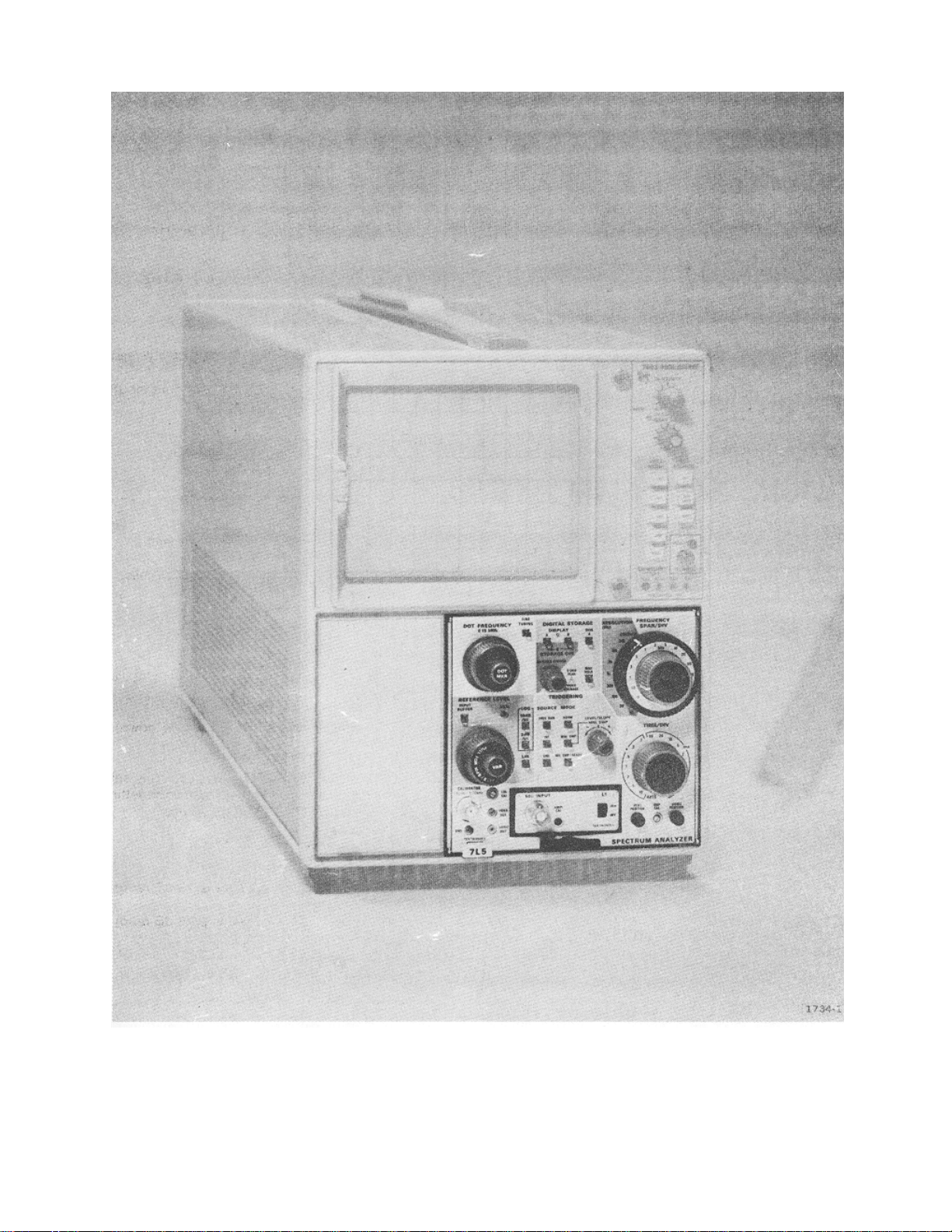
Fig. 1-1. 7L5 Spectrum Analyzer.
1-0
Page 7

SECTION 1. SPECIFICATION
Introduction
To effectively use the 7L5 Spectrum Analyzer,
the operation and capabilities of the instrument must be
known This instruction manual covers general operating
information about the instrument. Service information,
such as circuit description and c alibration are contained
in the Service manual.
TM 11-6625-2759-14 & P
Frequency Characteristics
Range
Input Frequency: 10 Hz through 5 0 MHz.
Dot Frequency: 0 Hz through 4999.75 kHz.
Description
The 7L5 is a 5 MHz spectrum analyzer with
digital storage. Frequency stability is within 5 Hz/hr and
center frequency (dot) can be read with six digit acc uracy
immediately after turn-on. There is no need to fine tune
the display Complex measurements and analysis can be
made with relative ease. Built-in micro-processing
circuits decode control settings, process frequency and
reference level information, and optimize sweep time and
resolution for the selected frequency span.
The 7L5 with 80 dB or more of spurious free
dynamic range, provides the ability to measure wide
relative amplitudes. Nanovolt sensitivity provides very
low-level signal and noise measurements.
The 7L5 display is fully calibrated in dBm, dBV,
or volts/div The reference level can be acc ur ately s et to 1
dB increments. A front panel input buffer control
increases front-end immunity to intermodulation distortion
while maintaining a constant reference level. To
accommodate a wide variety of impedance sources, the
7L5 uses quick disconnect plug-in input impedance
modules of 50 Ò, 75 Ò, 600 Ò, 1 MÒ/28 pF and
customized units to meet special requirements.
Digital storage allows any 7000-Series
mainframe, with crt readout, to present clean, easy to
photograph, displays. A smooth integrated display
provides an accurate analysis of most displays. Two
complete displays can be held in memory for comparis on
Two modes select either the conventional peak display or
a digitally averaged display.
ELECTRICAL CHARACTERISTICS
Accuracy
20àC to 30°C: +(5 Hz + 2 x 10
readout).
0°C to 50°C: ±(20 Hz + 10
readout).
Drift
5 Hz/hour or less.
Residual (Incidental) FM
50 Hz/div to 2 kHz/div: 1 Hz (p-p) or less.
5 kHz/div to 500 kHz/div. 40 Hz (p-p) or less.
Resolution Bandwidth
Accuracy
30 kHz--30 Hz: Within 20% of selected
resolution (6 dB down).
10 Hz: Within 100 Hz ±20 Hz (70 dB down).
The COUPLED setting electronically selects
the best resolution bandwidth for each setting of
the FREQUENCY SPAN/DIV control.
Shape Factor
30 kHz-3 kHz 5:1 or better (60:6 dB ratio).
1 kHz-10 Hz: 10:1 or better (60:6 dB ratio).
Amplitude Deviation
30 kHz-100 Hz: 0.5 dB or less.
-5
of dot
-6
of dot
The following electrical characteristics apply
when the 7L5 Spectrum Analyzer, in combination with a
Plug-In Module, are normally installed in a 7000-Series
oscilloscope and after a warm-up of ten minutes or more.
30 kHz-10 Hz: 2.0 dB or less.
1-1
Page 8

TM 11-6625-2759-14 & P
Input Characteristics
CAUTION
The application of a dc voltage to the INPUT of the L1 or
L2 Plug-In Modules may cause permanent damage to the
mixer circuit.
Input Impedance (Nominal):
L1 50Ò
L2 75Ò
L3 Selectable (50Ò, 600Ò, and 1 MÒ/28 pF).
Input Power (maximum Input level for refer ence
levels of 0 dBm or greater):
L1 21 dBm or 2.5 V rms
L2 21 dBm or 3.07 V rms
L3 21 dBm-input terminated 50Ò or 600Ò; 100
V (peak ac + dc) Input 1 MÒ/28 pF.
Input Power (maximum input level for reference
levels below 0 dBm):
L1 +10 dBm
L2 +10 dBm
L3 +10 dBm--input terminated 50Ò or 600Ò,
and 100 V (peak ac + dc) with input of 1 MÒ3/28 pF.
Equivalent Input Noise
Resolution (equal to or better than)
Bandwidth L1 L2 L3
10 Hz -135 dBm -135 dBm -148 dBV
30 Hz -133 dBm -133 dBm -146 dBV
100 Hz -130 dBm -130 dBm -143 dBV
300 Hz -125 dBm -125 dBm -138 dBV
1 kHz -120 dBm -120 dBm -133 dBV
3 kHz -115 dBm -115 dBm -128 dBV
10 kHz -110 dBm -110 dBm -123 dBV
30 kHz -105 dBm -105 dBm -118 dBV
NOTE
Sensitivity is degraded an additional 8 dB when the
INPUT BUFFER is on; e.g., at 3 kHz, the equivalent input
noise would be -107 dBm instead of -115 dBm. Noise
level will increase by approximately 10 dB when
operation Is In video peak mode,.
Intermodulation Distortion
Intermodulation products from two on-screen
signals, within any frequency span are >75 dB down for
third order products and at least 72 dB down for second
order products.
Second and third order intermodulation products
from two on-screen -53 dBV or less signals within any
frequency span are at least 80 dB down.
Amplitude Characteristics
NOTE
If digital storage is used, an additional quantization err or
of 0.5% of full screen should be added to the amplitude
characteristics.
Residual Response
Internally generated spurious signals are -130
dBm or less referred to the input (harmonics of the
calibrator are -125 dB) with L1 or L2 plug-in module and 143 dBV with the L3 plug-in module.
Sensitivity
The following tabulation of equivalent input noise for each
resolution bandwidth is measured with; the INPUT
BUFFER off, the VIDEO PEAK/AVG at m ax cw, and the
TIME/DIV set to 10 seconds.
With the INPUT BUFFER switch on, the second
and third order intermodulation products, for any two
onscreen signals, within any frequency span, are at least
80 dB down.
Display Flatness
Peak to peak deviation, over any selected
frequency span: Quantization error must be added (see
Note under Amplitude Characteristics ) if digital st orage is
used.
L1 0.5 dB;
L2 0.5 dB;
L3 0.5 dB
Reference Level
Refers to top graticule line in Log mode.
Calibrated in 1 dB and 10 dB steps for the L1 and L2
modules and 1 dB/2 dB and 10 dB for L3 plug-in m odule.
1-2
Page 9

TM 11-6625-2759-14 & P
Range L1 L2 L3
Log -128 dBm -128 dBm/ -128 dBm to
2 dB/Div to +21 dBm 139 dBV to +21 dBm (50Ò),
+21 dBm/ -139 dBm to
+10 dBV +10dBm (600Ò),
-141 dBV to
+8 dBV (Hi Z)
Log -70 dBm -70 dBm/ -70 dBm to
10 dB/Div
to +21 dBm
Incremental Accuracy
When calibrated at -40 dBV in Log mode.
L1, L2 and L3: Within 0.2 dB/dB with cumulative
error of 0.25 dB/10 dB.
Lin Mode Range: 20 nV/Div to 200 mV/Div within
5% in 1-2-5 sequence.
-81 dBV to +21 dBm (50Ò),
+21 dBm/ -81 dBm to
+10 dBV +10 dBm (600 Ò),
-83 dBV to
+8 dBV (Hi Z)
NOTE
A >sign is displayed adjacent to the reference level
readout when the reference level is not calibrated due to
an incompatible selection of controls.
Display Dynamic Range/Accuracy
Log 10 dB/DIV Mode: Dynamic window is 80 dB.
Accuracy is within 0.05 dB/dB to 2 dB maximum.
Log 2 dB/DIV Mode: Dynamic window is 16 dB.
Accuracy is within 0.1 dB/dB to 1 d,B maximum.
Sweep Characteristics
Frequency Span
Provides calibrated frequency spans from
50 Hz/div to max (500 kHz/div), within 4%, in 1-2-5
sequence.
Horizontal linearity is within 4% over the
entire 10 div display.
A 0-Hz/Div position is provided for time
domain operation.
Time per div is selectable from 10 s/Div to 0.1
ms/Div in 1-2-5 sequence. An AUTO position permits
automatic selection of optim um time/div for the selected
resolution and span/div settings.
Sweep rate accuracy is within 5% of the rate
selected.
Triggering
Provides two triggering sources, INT (internal)
and LINE, in addition to a FREE-RUN position.
When INT is selected, ac coupled signal
components from the mainframe T rigger Source (left or
right vertical amplifiers) are used.
When LINE is selected, ac coupled sample of
mainframe line voltage is used.
Three triggering modes are; NORM (normal),
SGL SWP/READY (single sweep), and MNL SWEEP
(manual sweep).
Trigger level is >1.0 div of internal signal for both
NORM and SGL SWP modes over the approximate
frequency range of 30 Hz to 500 kHz.
Output Connectors
Video Out
Front-panel pin jack connector s upplies the video
(vertical) output signal at an amplitude of 50 mV/div +5%
(about the crt vertical center) with source im pedanc e of 1
kÒ.
Horiz Out
A front-panel pin jack connectorsupplies
horizontal output signal (negative-going sawtooth that
varies from 0.0 V dc to approximately -6 V dc with a
source impedance of 5 kÒ.
Calibrator
Front panel BNC connector supplies a calibrated
500 kHz squarewave output signal (derived from the
analyzer’s time base). Output amplitude is within +0.15
dB of -40 dBV into impedance of the plug-in module.
Sweep Rate
1-3
Page 10

TM 11-6625-2759-14 & P
ENVIRONMENTAL CHARACTERISTICS
The 7L5 Spectrum Analyzer will meet the
foregoing electrical characteristics within the
environmental limits of a 7000-Series oscilloscope.
Complete details on environmental test procedures
including failure criteria etc., can be obtained from a local
Tektronix Field Office or representative.
PHYSICAL CHARACTERISTICS
Net weight (instrument only), 8 pounds, 12
ounces.
ACCESSORIES AND OPTIONS
Standard Accessories Tektronix Part No.
Graticule, Spectrum
Analyzer 377-1159-02 (7000-Series)
Filter, light amber 378-0684-00
Manual, Operating 070-1734-00
Manual, Service 070-2184-00
Optional Accessories
Plug-in Module,
50 ohm L1
Plug-in Module,
75 ohm L2
Plug-in Module
50 Ò 600Ò &
1 MÒ/28 pF L3
Probe (10X) P6105 (see L3 Manual)
Attenuator, step.
50 ohm 2701
Attenuator, step,
75 ohm 2703
OPTIONS
7L5 Option 21 -(Log Display)
7L5 Option 25--(Tracking Generator)
7L5 Option 28--(Readout)
7L5 Option 30-(Option 21/25)
7L5 Option 31 -(Option 21/28)
7L5 Option 32-(Option 25/28)
7L5 Option 33--(Options 21/25/28)
1-4
Page 11

SECTION 2. INSTALLATION
TM 11-6625-2759-14 & P
Initial Inspection
This instrument was inspected both mechanic ally
and electrically before shipment. It should be free of
mars or scratches and electric ally meet or exceed all
specifications. Inspect the instrument for physical
damage and check the electrical performance by the
Operational Check procedure provided within these
instructions. This procedure will verify that the
instrument is operating correctly and it will satisfy most
receiving or incoming inspection requirements. If all
instrument specifications are to be verified, refer to the
Service Instructions for the 7L5.
If there is physical damage or performance
deficiency, contact your local Tektronix Field Office or
representative
Installation
To install the 7L5, align the upper and lower
guide rails with those in the receiving compartments of
the mainframe. Slide the instrument along the rails into
the mainframe When the electrical connectors at the rear
of the 7L5 make contact, apply firm, steady pressure to
the front panel until the rear connectors are engaged and
the front panel is approximately flush with the
oscilloscope front panel. To remove the 7L5, pull the
release latch labeled 7L5, at the lower left of the front
panel, and remove the instrument.
REPACKAGING FOR SHIPMENT
Include complete instrument serial number and
description of the service required.
Save and re-use the container your instrument
was shipped in. If the original packaging is not available
or is unfit for use, repackage as follows:
1. Obtain a shipping container of heavy
corrugated cardboard or wood with inside dimensions six
inches or greater than the instrument dimensions. This
will allow room for cushioning. Refer to Table 2-1 for
carton test strength requirements.
2. Wrap the instrument in heavy paper or
polyethylene sheeting to protect the instrument finish.
Protect the front panel with urethane foam or cardboard
strips.
3 Cushion the instrument on all sides by
packing dunnage or urethane foam between the carton
and the instrument, allowing three inches on all sides.
4. Seal the shipping carton with shipping tape
or an industrial stapler.
TABLE 2-1
Gross Weight (lb) Carton Test Strength (lb)
0-10 200
10-30 275
30-120 375
120-140 500
140-160 600
If your Tektronix instrument is to be shipped to a
Tektronix Service Center for service or replacement,
attach a tag showing; owner (with address) and the name
of an individual, at your firm, that can be contacted.
If you have any questions, contact your local
Tektronix Field Office or representative.
2-1
Page 12

SECTION 3. OPERATING INSTRUCTIONS
Introduction
This section contains; a simplified block diagram
description, function of the front panel controls and
connectors, an operational check-out and familiarization
procedure, and a section devoted to the use and
application of the instrument. Service information is
contained in the Service Instruction manual.
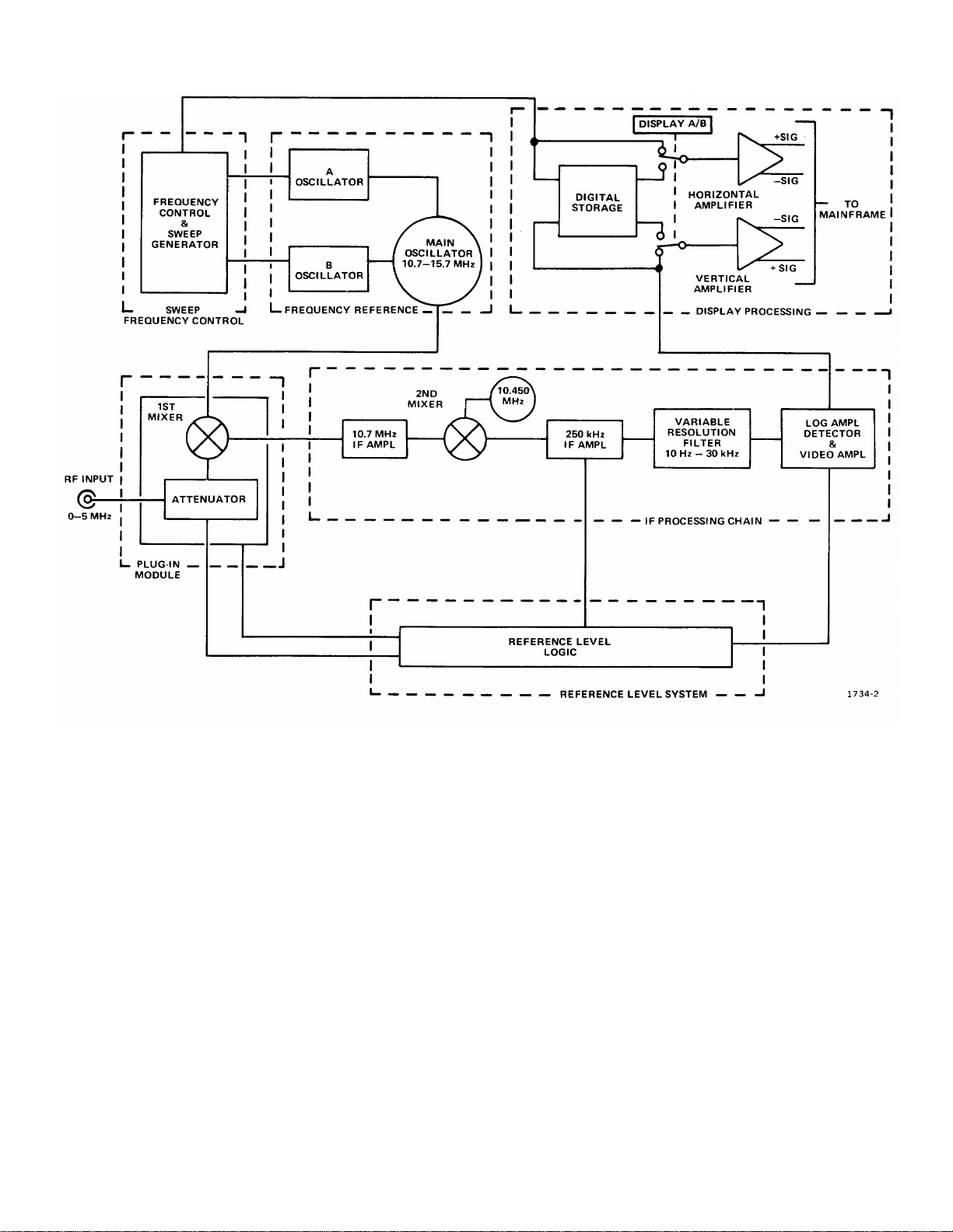
FUNCTIONAL BLOCK DESCRIPTION
Functional Block Description
The 7L5 is a swept front end spectrum analyzer
with selectable front-end plug-in modules that permit the
user to obtain calibrated display for a number of different
Impedances (i.e., 50 ohm, 600 ohm, etc.). The plug-in
module contains; selectable attenuation, the first mixer,
and an Input buffer selector that trades attenuation for IF
gain. Signal attenuation in the plug-in and gain of the IF
processing chain are controlled by a r eference level logic
circuit in the 7L5 which provides calibrated settings in 1
dB or 10 dB steps over a range of approximately 146 dB
(depending on the plug-in module). A simplified block
diagram is shown in Fig. 3-1.
The input signal to the 7L5 is mixed with the
frequency of the main oscillator and the IF of 10. 7 MHz is
fed to and amplified by the 10.7 MHz IF amplifier. Since
the 7L5 input frequency range is O to 5 MHz, the main
oscillator is tuned and swept from 10.7 to 15.7 MHz. The
frequency of the main oscillator is controlled by two
secondary (A and B) oscillators that use a synthesizer
technique to tune and phase lock their frequencies. The
sweep frequency control circuit drives the oscillators
TM 11-6625-2759-14 & P
according to the settings of front panel DOT
FREQUENCY and FREQUENCY SPAN/DIV controls.
The 10 7 MHz IF is processed through bandpass
filters and amplifiers and then mixed with the output from
a 10.450 oscillator, to down-convert the 10.7 MHz to an
IF of 250 kHz Gain of the 250 kHz amplifier is c ontrolled
by the reference level logic circuit which establishes the
amount of attenuation in the plug-in module and gain for
the 250 kHz IF and Log amplifiers. The reference level is
selectable in 1 dB and 10 dB steps.
The 250 kHz IF signal is processed through the
variable resolution filter circuits for bandwidth selec tions
of 10 Hz to 30 kHz. The signal is again amplified,
detected, and the video is sent through amplifier circuits
that provide the 10 dB/dlv, 2 dB/dlv, and linear gain
characteristics.
The video signal is then fed to the display
processing circuits where the signal is either stored and
displayed, or, if the storage mode is not selected, the
signal is passed directly through the vertical output
amplifier to the mainframe circuit. If either or both the
DISPLAY A or DISPLAY B latches are enabled, the
signal is converted to digital data, stored in A or B
memory, then converted back to analog data and
processed through the output amplifiers to the mainframe
The vertical information is digitized and stored at 512
horizontal address locations across the screen.
Therefore, the horizontal sweep information is converted
to digital data for storage, then converted back to an
analog signal for display The horizontal sweep ramp is
processed the same as the vertical s ignal. The vertical
(video) information can be averaged or peak detected.
3-1
Page 13
TM 11-6625-2759-14 & P
Fig. 3-1. Functional block diagram.
3-2
Page 14

FRONT PANEL CONTROLS AND
CONNECTORS
Pushing any front panel pushbutton switch
activates a bistable electronic circuit to c hange its output
state. When in the active state, the plastic pus hbutton is
illuminated. Pressing the pushbutton a second time
changes the output of the circuit to the inactive state and
extinguishes the illuminated button.
Front panel controls also include two special
photo-optic switch assemblies, the FREQUENCY
SPAN/’DIV-RESOLUTION switch and the TIME/DIV
switch. Designed especially for the 7L5, each assem bly
is a mechanical/photo-electric, digital switch, that
provides a TTL compatible five-bit binary output. The
reliability of these switches has been demonstrated and
with normal use they should last the life of the
instrument. Dism antling or field repair of these switches
is discouraged since their proper operation requires
precision alignment of their internal components. If either
switch assembly is damaged or suspected of
malfunction, it should be replaced as an assembly.
The following describes the function of the front
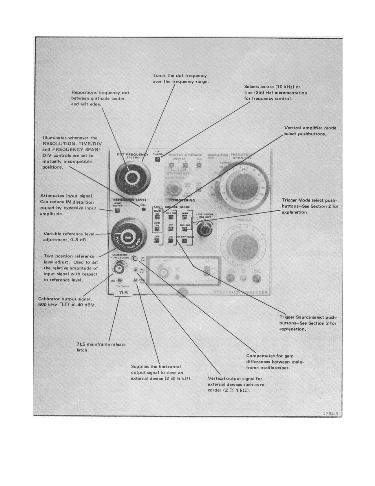
panel selectors for the 7L5. A layout of the front panel is
shown in Fig. 3-2.
DOT FREQUENCY Changes the dot (marker)
frequency in coarse (10 kHz) or
fine (250 Hz) steps over the input
frequency range of 0 Hz to 5 MHz.
The frequency of the dot mark er is
displayed on the crt readout in the
upper right set of character s. Dot
frequency will not extend beyond
the 7L5 frequency range, even if
the control is rotated. When power
is applied, dot frequency starts at
0.000.
FINE TUNING Selects coarse or fine
incrementation for the DOT
FREQUENCY control. When the
FINE TUNING switch is activated
(illuminated), each rotational click
of the DOT FREQUENCY control
changes the dot frequency in
increments of 250 Hz. When the
FINE TUNING switch is inactive
(extinguished), each rotational
click of the DOT FREQUENCY
control changes the dot frequency
in increments of 10 kHz.
TM 11-6625-2759-14 & P
DOT MKR Used to horizontally position the
frequency dot. The displayed
frequency readout characters
enumerate the actual frequency of the
dot. When the DOT MKR control is in
its detent position (fully ccw), the
frequency dot and the selected
frequency are on the vertical center
line of the graticule. The 7L5 can be
operated in a start sweep mode when
the frequency dot is positioned to the
left vertical graticule line. The DOT
MKR control is disabled when the
FREQUENCY SPAN/DIV switch is at
MAX.
REFERENCE Sets the full screen signal amplitude
LEVEL level (dBm, dBV) required at the
INPUT to the plug-in module. This
level is relevant to the input impedance
of the plug-in module. Ref erence level
is associated to the top graticule line of
the display area and signal level is
relative to this reference. The
reference level range depends on the
plug-in module, however, in the 2
dB/Div mode it covers 149 dB, in the
10 dB/Div mode the range is 90 dB
and in the Lin mode 20 nV/div to 200
mV/div. The control has two speeds or
stepping increments; pulled out, each
increment is 10 dB, pushed in each
increment is 1 dB or in some cases
(dependent on the plug-in module) 2
dB.
VAR The VAR (variable) control provides 8
dB or more gain adjustment
between each calibrated reference
level step. A<symbol is displayed on
the crt, preceding the reference level
readout, whenever the reference level
is not calibrated (VAR is not in its
detent position).
INPUT BUFFER The active (illuminated) state of this
pushbutton switch inserts 8 dB of
signal attenuation at the input of the
first mixer and adds 8 dB of vertical
gain (after the variable resolution
filters). When used, it reduces
intermodulation distortion caused by
excessive input signal amplitude.
Because of its increased gain, the
noise figure is increased 8 dB when
this switch is activated.
3-3
Page 15
TM 11-6625-2759-14 & P
Fig. 3-2.A. 7L5 front panel controls and connectors.
3-4
Page 16
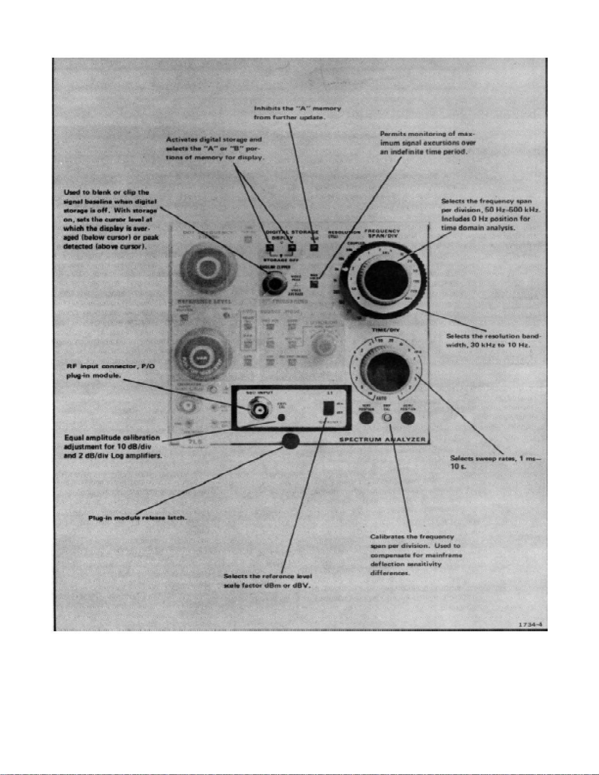
TM 11-6625-2759-14&P
Fig. 3-2B. 7LS-L1 plug-in front panel control and connectors.
@ 3-5
Page 17

TM 11-6625-2759-14&P
LOG 10 dB/DIV The illuminated condition of this
pushbutton selects a logarithmic
display of 10 dB/div with a dynamic
range of 80 dB.
LOG 2 dB/DIV The illuminated condition of this
pushbutton selects a logarithmic
display of 2 dB/div with a dynamic
range of 16 dB
LIN The illuminated condition of this
pushbutton selects a linear display.
Signal amplitude is a linear function of
input level.
FREQUENCY Selects frequency spans from
SPAN/DIV 50 Hz/div to 500 kHz/div (MAX
position). A 0 Hz position provides
time domain display with a bandpass
dependent on the setting of the
RESOLUTION selector. In the 0 Hz
position the frequency dot is not
displayed and when in the MAX
position the frequency dot position is
controlled by the DOT FREQUENCY
control.
RESOLUTION Selects resolution bandwidths of 10
Hz to 30 kHz in a 1-3 sequence. A
COUPLED position electronically
selects the best compatible resolution
bandwidth setting for the
FREQUENCY SPAN/DIV selection.
TIME/DIV Selects the analyzer’s sweep rate.
Sweep rates are 10 s/div to 0.1
ms/div in a 5-2-1 sequence. An AUTO
position electronically programs sweep
rate so the display remains calibrated
for the selected frequency span and
resolution bandwidth settings.
UNCAL When the display is uncalibrated
because the FREQUENCY
SPAN/DIV, RESOLUTION, and
TIME/DIV switch settings are
incompatible, this indicator lights and a
> symbol is displayed on the crt as a
prefix to the reference level readout
characters.
TRIGGERING Two trigger sources (Line and Internal)
plus a Free Run mode can be
selected. In the Free Run mode
(FREE RUN button activated) the
sweep free runs and will not sync with
any trigger signal. When the LINE
pushbutton is activated (illuminated)
the sweep is triggered by the line
voltage to the mainframe. The INT
pushbutton selects ac coupled signal
components from the mainframe
Trigger Source (left or right vertical).
Three trigger modes are provided:
NORM (normal), SGL SWP/READY
(single sweep/ready) and MNL
SWEEP (manually controlled sweep).
When the NORM button is activated,
the sweep is triggered from the s our ce
selected; or, if the trigger is not
present, the sweep automatically runs
in about 10-second intervals to provide
a baseline display. When the SGL
SWP/READY button is activated, the,
sweep runs with the next trigger or in
about 10 seconds if trigger is not
present. In time domain operation
(FREQ SPAN/DIV at 0 Hz) pushing
the button activates the sweep ready
state. The button lights to indicate the
trigger circuit is arm ed and ready. The
sweep will run with the arrival of a
trigger. The button remains
illuminated until the sweep has
completed its run. This provides a
ready indication of the sweep state
when photographing a display.
LEVEL/SLOPE- A dual function control. As a level
MNL SWP slope/control, it adjusts the level of the
trigger threshold on either a positive or
negative slope. As a manual sweep
control, it positions the crt beam
anywhere along the X- axis.
Maximum cc w corresponds to a beam
location at the left graticule edge.
DIGITAL SAVE A: Activating the SAVE A
STORAGE pushbutton dedicates one half of the
digital storage mem ory to preserve the
binary equivalent of the existing
waveform amplitude at 256 X-axis
locations. The A memory is inhibited
from further update until SAVE A is
deactivated (extinguished).
@ 3-6
Page 18

TM 11-6625-2759-14&P
DISPLAY A/B: When DISPLAY A or
DISPLAY B is selected, the
corresponding pushbutton switch is
illuminated and the contents of
memory A or memory B is displayed.
With SAVE A of f, all m e m ory locations
are displayed contiguously. With
SAVE A on, DISPLAY A and DISPLAY
B are selected. The con- tents of both
memories are interlaced and
displayed.
PEAK AVERAGE/BASELINE
CLIPPER: A dual function control.
When digital storage is of f, this c ontrol
operates as a conventional baseline
clipper, i.e., as the control is rotated
ccw, more of the vertical display is
progressively blanked or clipped over
the last 1/3 turn of the control. W hen
digital storage is on, the PEAK
AVERAGE control sets the level at
which the vertical display is either
peak detected or digitally averaged.
Video signals above the level set by
the PEAK AVERAGE control (and
denoted by a horizontal cursor) are
peak detected and stored. Video
signals below the level set by the
PEAK AVERAGE control are digitally
averaged and stored.
MAX HOLD: Enables the digital
storage memory to store the
maximum signal levels within the
period the circuit is active (button
illuminated). This maximum signal
can then be saved and com pared with
future signals for drift or amplitude
variations.
SWP CAL Adjusted during the operational check
to calibrate the sweep. This
adjustment compensates for
differences in deflection sensitivity
between mainframe oscilloscopes.
The SWP CAL control should be
adjusted or checked for pr oper setting
each time the 7L5 is installed in an
oscilloscope.
LOG CAL Adjusted during the operational
check to calibrate the 2 dB/div and the
10 dB/div displays. This adjustm ent is
used to compensate for differences in
vertical gain between mainframe
oscilloscopes. The LOG CAL control
should be adjusted or checked for
proper setting each time the 7L5 is
installed in an oscilloscope.
AMPL CAL (L1 The AMPL CAL control is adjusted
Plug-In Module) during the initial calibration to
calibrate the full screen reference
level. This control is used to
compensate for gain dif ferences in the
RF and IF portions of the instrument.
The AMPL CAL control should be
adjusted or checked for pr oper setting
each time a plug-in m odule is installed
in the 7L5.
HORIZ POS Positions the display or baseline on
the crt X-axis.
VERT POS Positions the display or baseline on
the crt Y-axis.
dBm/dBV Located on the plug-in module front
panel, the dBm/dBV control selects
the reference level scale factor;
decibels with respect to one milliwatt
or decibels with respect to one volt.
Calibrating the 7L5 to the Oscilloscope Mainframe
1. Install or verify the presence of a plug-in
module (see Optional Accessories, Section 1)
2. Select oscilloscope Vertical Mode,
Horizontal Mode and Trigger Source (Right or Left)
corresponding with plug-in compartments occupied by
the spectrum analyzer. Turn on the mainframe power
and allow a 10 minute warm-up period.
3. Set the front panel controls as follows:
DOT MKR max ccw (detent position)
FREQUENCY
SPAN/DIV MAX (500 kHz)
RESOLUTION COUPLED
VAR max ccw (detent position)
BASELINE
CLIPPER max cw
LOG 10 dB/DIV on
REFERENCE LEVEL -40 dBV
INPUT BUFFER off
FREE RUN on
NORM on
SAVE A off
MAX HOLD off
dBm/dBV dBV (plug-in module
switch)
TIME/DIV AUTO
@ 3-7
Page 19
TM 11-6625-2759-14&P
4. Connect the CALIBRATOR signal to the
INPUT connector on the plug-in module with a short
length of coaxial cable. Adjust the SW P CAL and the
HORIZ POSITION controls to align the s econd and tenth
vertical signals with the second and tenth vertical
graticule lines counting from the left edge.
5. Set the FREQUENCY SPAN/DIV to 2 kHz,
Display Mode 2 dB/div, and DISPLAY A and B on.
Adjust the VERT POSIT ION control to place the display
baseline on the bottom horizontal graticule line.
6. Set RESOLUTION control to 3 kHz and
DOT FREQUENCY to 500.00 kHz.
7. Select the LOG 10 dB/DIV pushbutton and
adjust the LOG CAL control fo r a full screen (8 division)
display.
8. Select the LOG 2 dB/DIV pushbutton and
adjust the AMPL CAL (on plug-in module) for a full
screen display.
9. Repeat steps 7 and 8 until the displayed
waveforms are 8 vertical divisions in both log amplifier
settings. (Refer to Fig. 3-3, Log Amplifier Calibration
Composite W aveform.) If desired, check linearity of the
10 dB/div display by increasing the REFERENCE LEVEL
in 10 dB steps. Adjust LOG CAL slightly to correct any
non- linearity.
OPERATIONAL CHECKOUT
Introduction
This is an operational checkout procedure
intended to satisfy most custom er’s receiving inspection
requirements and to provide instrument familiarization for
the new user We recommend using this checkout as part
of the users routine maintenance program and a
preliminary check before performing the Performance
Check portion of the Service Instruction manual.
The front panel CALIBRATOR output is an
accurate signal source and is used in the following
procedures to verify operational status of the instrum ent.
Calibrator frequency accuracy may be verified by
applying it to an accurate digital counter.
Some procedures require a s tep attenuator and
two short lengths of coaxial cable. To verif y the absolute
reference level specifications, the attenuator accuracy
must be calibrated or verified at some specific frequency,
to within 0.03 dB/dB with a cumulative error not to
exceed 0.1 dB for any change up to 10 dB. Incremental
accuracy can be verified and a good indication of the
absolute reference level accuracy can be obtained by
using two Tektronix Step Attenuators, such as the 2701
(see Optional Accessories, Section 1). These
attenuators provide a good indication of oper ation even
though their accuracy specifications are not within the
limits described.
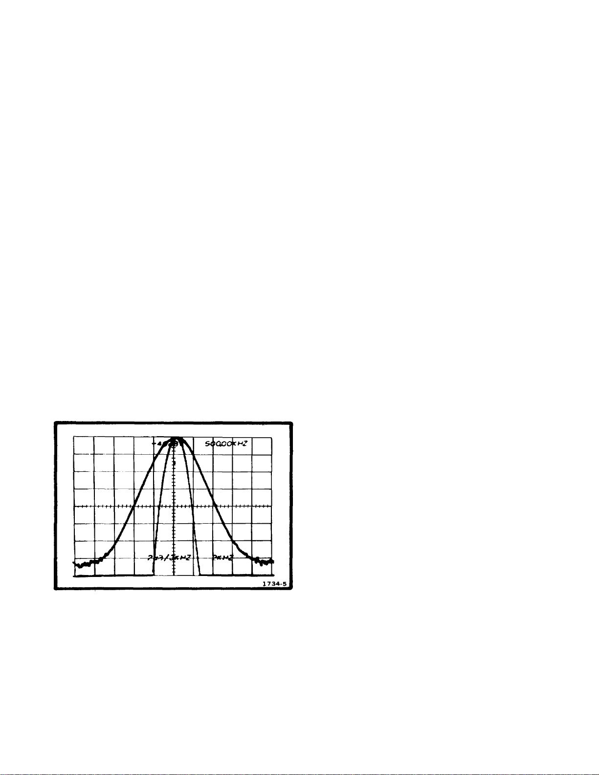
Fig. 3-3. Log amplifier calibration composite waveform.
1. Preliminary Preparation
Preset the front panel controls and selectors as
described under Calibrating the 7L5 to the Osc illoscope
Mainframe and perform the calibration procedure as
previously described.
2. Operational Check of Readout Characters
With the 7L5 installed and operating in a 7000Series mainfram e, perform the following steps to c heck
the readout operation.
Dot Frequency Readout
a. Verify that the dot frequency readout is 0.00
kHz after initial turn-on. (Readout characters f or the dot
frequency are located near the top edge of the crt and
can be identified by the suffix characters kHz).
b. With the FINE TUNING pushbutton not
illuminated (inactive), verify that the DOT FREQUENCY
control changes the value of the readout characters in 10
kHz increments.
@ 3-8
Page 20

TM 11-6625-2759-14&P
c. Rotating DOT FREQUENCY control cw
should increase the readout and ccw rotation should
decrease the readout.
d. Activate the FINE TUNING pushbutton and
verify that the DOT FREQUENCY control changes the
value of the readout characters in 250 Hz increments.
e. Verify that continuous cw rotation of the
DOT FREQUENCY control causes no change of the
readout characters after an indicated 4999.75 kHz.
NOTE
Following a change of the DOT FREQUENCY
control, the first click in the opposite direc tion will
have no effect.
Reference Level Readout (L1 Plug-In Module)
f. Select the LOG 2 dB/DIV mode and set the
dBm/dBV switch (on the plug-in m odule) to dBm. Verify
that the indicated value of the reference level changes by
13 dB (e.g., -40 dBV = -27 dBm). Reference level
readout characters are located near the top edge of the
crt and can be identified by the suffix charac ters dBm or
dBV.
g. With the UNCAL light off, rotate the VAR
(variable) control and verify that a < symbol (not
calibrated) prefixes the refer ence level readout. Rotate
the VAR control to its maximum ccw (detent) position
and verify that the < symbol is no longer displayed.
h. Pull the REFERENCE LEVEL control out to
its coarse position and verify that the value of the
reference level readout changes in 10 dB steps. Push
the REFERENCE LEVEL control in to its fine position
and verify that the value of the reference level readout
changes in 1 dB steps.
i. Verify, that rotation of the REFERENCE
LEVEL control beyond the reference level limits of ; -128
dBm (-141 dBV), In the 1 dB/step position, or; -70 dBm (83 dBV) in the 10 dB/step position-for the one extrem eand +21 dBm (8 dBV) for the other extreme remains
constant. (These extrem es are applicable only for 50 Ò
plug-in modules.)
J. With the REFERENCE LEVEL control at
max ccw position, select the LIN mode and verify that the
readout changes to 200 mV.
k. Rotate the REFERENCE LEVEL cw and
verify that the readout changes from m V to ÎV to nV in a
2-1-5 sequence. Verify that continuous cw rotation of the
REFERENCE LEVEL control causes no change of the
corresponding readout characters beyond 20 nV.
Time/Div Readout
I. Set the FREQUECNY SPAN/DIV switch to
0. Rotate the TIME/DIV control to each of its positions
and verify that its front panel designations corres pond to
the crt readout characters. (Readout c haracters for the
sweep time per division are located near the bottom r ight
edge of the crt and can be identified by the suffix
character S when the FREQUENCY SPAN/DIV is set to
0.)
Frequency Span/Div Readout
m. Set TIME/DIV control to AUTO and the
RESOLUTION control to COUPLED. Rotate the FREQUENCY SPAN/DIV control to each of Its positions and
verify that the readout characters correspond with the
front panel designations and change In accordanc e with
the readout listed in Table 3-1. (Readout characters f or
frequency span per division setting occupy the sam e crt
position as the time per division readout characters.
They are located near the bottom edge of the crt and
except for the 0 span setting, can be identified by the
suffix characters Hz.)
TABLE 3-1
FREQUENCY SPAN/DIV FREQUENCY
SPAN/DIV
control settings readout
0 10 ms
50 (Hz) 50 Hz
1 kHz 100 Hz
.2 kHz 200 Hz
.5 kHz 500 Hz
1 kHz 1 kHz
2 kHz 2 kHz
5 kHz 5 kHz
10 kHz 10 kHz
20 kHz 20 kHz
50 kHz 50 kHz
.1 MHz 100 kHz
.2 MHz 200 kHz
MAX 500 kHz
Resolution Readout
n. Rotate the RESOLUTION control to eac h of
its: positions and verify that the readout characters
correspond with the front panel designations. ( Readout
characters for the resolution function are located near
the bottom edge of the crt and can be identified by the
suffix characters Hz.)
@ 3-9
Page 21

TM 11-6625-2759-14&P
o. With the RESOLUTION control in the
COUPLED position, rotate the FREQUENCY SPAN/DIV
to each of its positions and verify that the RESOLUTION
readout characters change in accord with Table 3-2.
TABLE 3-2
FREQUENCY
SPAN/DIV
control settings readout
MAX (500 kHz) 30 kHz
200 kHz 30 kHz
100 kHz 30 kHz
50 kHz 10 kHz
20 kHz 3 kHz
10 kHz 3 kHz
5 kHz 1 kHz
2 kHz 300 Hz
1 kHz 300 Hz
.5 kHz 100 Hz
2 kHz 30 Hz
.1 kHz 30 Hz
50 (Hz) 10 Hz
0 30 kHz
RESOLUTION
NOTE
The full dynamic range of the Log 10
dB/div and the Log 2 dB/div is not
measured in the following paragraphs. If
the log amplifiers include a negative
error, full range verification would
require signal level measurem ent below
the display baseline. Since this is not
possible, the following steps verify 78 of
the 80 dB range and 15 dB of the 16 dB
range for the two log amplifier
selections.
LOG 10 dB/DIV (Dynamic window is 80 dB,
accuracy is ±0.05 dB/dB to 2 dB maximum)
a. Set the 7L5 controls as follows:
DOT FREQUENCY 500.00 kHz
RESOLUTION COUPLED
FREQUENCY SPAN/DIV 0.1 kHz
TIME/DIV AUTO
REFERENCE LEVEL -40 dBV
dBm/dBV (L1 Plug-in) dBV
Vertical Amplifier Mode Readout
p. Select the 10 dB/DIV pushbutton switch and
verify that the readout characters for the vertic al amplifier
mode indicate 10 dB/ Readout characters for the vertical
amplifier mode are loc ated near the lower edge of the c rt
and for the log positions, can be identified by the suffix
symbol /.
q. Select the 2 dB/DIV mode and verify that
the readout characters indicate 2 dB/.
r. Push the LIN pushbutton and verify an
absense of readout characters for vertical amplifier
mode.
Uncalibrated Readout
s. Set the RESOLUTION control to COUPLED
and the FREQUENCY SPAN/DIV control to MAX.
Rotate the TIME/DIV cw until the UNCAL light is
illuminated. Verify that a > symbol prefixes the
referenced level readout characters. Rotate the
TIME/DIV ccw until the UNCAL light is extinguished
Verify that the > symbol is no longer displayed
b. Apply the CALIBRATOR signal through
external attenuator(s), such as Tektronix, 2701 (for 50
Ò)-see Optional Accessories in Section 1-to the INPUT
connector. Select the LOG 10 dB/DIV pushbutton.
c. Increase external attenuation in 10 dB steps
to 70 dB and verify that each step decreases the
displayed f signal level 10 dB ±0.5 dB.
d. Increase external attenuation by 8 dB (for a
total of 78 dB) and verify that the total overall decrease in
signal amplitude is 78 dB ±2 0 dB.
LOG 2 dB/DIV (Dynamic window is 16 dB,
accuracy is ±0.01 dB/dB to ±1 dB maximum)
e. Set the external attenuators to 0 dB. Set
the FRE- QUENCY SPAN/DIV to 50 Hz, RESOLUTION
to 30 Hz and select the 2 dB/DIV pushbutton.
f. Add 15 dB attenuation, with the external 1
dB step attenuator, in 2 dB and 1 dB increments. Verify
that the signal level change, is within 0.1 dB/dB of added
attenuation to a maximum of 1.0 dB deviation over the
15 dB range.
3. Dynamic Range
LIN Linearity
g. Select the LIN pushbutton and adjust
the REFERENCE LEVEL control for a crt readout of 500
pV/ (per division).
@ 3-10
Page 22

h. Add 10 dB of external attenuation. Adjust
the VAR control for a signal display amplitude of 8
divisions.
i. Add 6 dB of external attenuation. Verify
that the signal amplitude decreases to 4.0 ±0.2 division
(±5%) or half amplitude.
j. Add an additional 6 dB of external
attenuation and verify that the display amplitude
decreases to 2.0 ±0.1 division.
VARiable Control Range
k. Inser t 10 dB of external attenuation. Select
the 2 dB/DIV pushbutton and rotate the VAR control fully
cw. Adjust the REFERENCE LEVEL to set the displayed
signal amplitude to a vertical reference point near full
screen.
I. Rotate the VAR control fully ccw (detent
position). Verify that the signal amplitude decreases at
least 4.0 divisions. Decrease external attenuation to
return the signal amplitude to the reference point and
verify that the required change was 8 dB or more.
4. Reference Level Accuracy (within 0.2 dB/dB
with a cumulative error not to exceed 0.25 dB for any
change up to 10 dB)
The external attenuator accuracy requirements
to perform this step, have been described in the
Introduction to this Operational Check procedure.
Reference level increments are 1 dB and 10 dB steps.
Circuitry of the 7L5 provides 1, 2, 4, 8, and 16 dB gain
steps. These steps, or combinations of the steps,
provide the reference level range. This procedure
checks the accuracy of each gain cell and thus the
overall accuracy. The accuracy of the V/Div mode will be
within that specified if the Log mode reference level is
within limits. A few check points may be perform ed as
listed in Table 3-4 to spot check Lin mode operation.
TM 11-6625-2759-14&P
c. Change the REFERENCE LEVEL control to
-30 dBm. Increase the exter nal attenuation 1 dB (3 dB
total) and verify that the signal peak is within 0.2 dB of
the reference point established in step b.
d. Rotate the REFERENCE LEVEL control to 31 dBm. Increase the external attenuation another 1 dB
(4 dB total) and verify that the signal peak is within 0.25
dB of the reference point.
e. Readjust the VERT POSITION control, as
required, to establish a new graticule reference point for
the signal peak.
f. Pull the REFERENCE LEVEL control out to
the 10 dB/step position and set it for a crt readout of -41
dBm. Increase the external attenuation 10 dB (14 dB
total) and verify that the signal level is within 0.25 dB of
the reference point established in step e.
g. Check the Reference Level accurac y for the
remaining range by following the settings listed in Table
3-3 and noting the error.
TABLE 3-3
Reference Level External Attenuation Allowable
Limits
(dBm) (dB) (dB)
-41 14 0.25
-51 24 0.50
-61 34 0 75
-71 44 1.00
-81 54 1.25
-91 64 1.50
-101 74 1.75
-111 84 2.00
-121 94 2.25
LIN Accuracy
This procedure uses a 50 0 plug-in module (L1):
a. Switch the dBm/dBV selector (on the plug-
in module) to dBm and set the 7L5 controls as follows:
REFERENCE LEVEL -29 dBm
RESOLUTION 3 kHz
FREQEUNCY SPAN/DIV 1 kHz
TIME/DIV AUTO
b. Set the external attenuation to 2 dB and
adjust the REFERENCE LEVEL for a readout of -29
dBm. Adjust the VERT POSITION control slightly, as
required to establish a graticule reference point for the
signal peak.
g. Set the external attenuator to 0 dB. Select
the LIN pushbutton and adjust the REFERENCE LEVEL
control for a crt readout of 10 mV.
h. Set the external attenuator and the
REFERENCE LEVEL control to the positions listed in
Table 3-4. Check that the measured s ignal amplitudes
are in accordance with those listed in Table 3-4.
@ 3-11
Page 23

TM 11-6625-2759-14&P
TABLE 3-4
Reference Signal
Attenuator Voltage Level Amplitude
Setting (dB) Input Volts/DIV
0 10 mV 2 mV 5
20 1 mV 0.2 mV 5
40 100 ÎV 20 ÎV5
60 10 ÎV2 ÎV5
80 1.0 ÎV 200 nV 5
5. Input Buffer (Operational check only)
a. Apply the CALIBRATOR signal to the
INPUT on the plug-in module. Set the 7L5 front panel
controls as follows:
DOT FREQUENCY 500.00 kHz
RESOLUTION 3 kHz
FREQUENCY SPAN/DIV 1 kHz
TIME/DIV AUTO
INPUT BUFFER Off
LOG 2 dB/DIV On
b. Establish a signal amplitude of 7 divisions
with the REFERENCE LEVEL control
c. Switch the INPUT BUFFER on and verify
that the display amplitude does not change more than 1
dB (.05 div).
d. Change the RESOLUTION to 10 kHz and
check amplitude change of the calibr ator signal with the
INPUT BUFFER on and off.
6. Residual (Incidental) FM (Incidental FM is <1
Hz, 50 Hz/div to 2 Hz/div and <40 kHz, 5 kHz/div to 500
kHz/div)
a. With the CALIBRATOR signal applied to the
INPUT of the plug-in module, set the 7L5 front panel
controls as follows:
DOT FREQUENCY 500.00 kHz
REFERENCE LEVEL -57 dBM
RESOLUTION COUPLED
FREQUENCY SPAN/DIV 50 (Hz)
TIME/DIV AUTO
LOG 2 dB/DIV On
INPUT BUFFER Off
DIGITAL STORAGE Off
b. Select the MNL SWP pushbutton and
adjust the MNL SWP control to place the trace dot
halfway up one side of the displayed 10 Hz filter
waveform, near center screen. Verify that incidental FM
(short term, peak to peak movem ent of trace dot) is less
than 1.0 vertical division (1 Hz).
in Div’s ±5%
c. Set the RESOLUTION control to 300 Hz,
the FREQUENCY SPAN/DIV to 5 kHz, and the
REFERENCE LEVEL to -62 dBm. Adjust the MNL
control to place the trace dot halfway up one side of the
displayed 300 Hz filter waveform, near center screen.
Verify that maximum vertical jitter of the trace dot does
not exceed 1.2 division (40 Hz)
7. Residual Response (Plug-in module
dependent. Internally generated spurious signals are
down 130 dB or more with the L1 Plug-In Module)
NOTE
Each 7L5 Spectrum Analyzer is
carefully tested at the factory to ensure
that all internally generated spurious
responses are below-130 dBm.
Thorough verification of this
specification would take several days.
A procedure to check the f ull frequency
range (to - 110 dBm) and to spot check
100 kHz of the total frequency range, to
-130 dBm is given in the following
steps. The 100 kHz frequency range
chosen is 300 through 400 kHz. The
procedure can also be used to spot
check any 200 kHz span within the 0-5
MHz capability of the instrument.
a. Terminate the input connector with a
resistive load that equals the characteristic input
impedance of the plug- in module. Set the 7L5 front
panel controls as follows:
DOT FREQUENCY 500.00 kHz
RESOLUTION 300 Hz
FREQUENCY SPAN/DIV 100 kHz
TIME/DIV AUTO
LOG 10 dB/DIV On
REFERENCE LEVEL -70 dBm
INPUT BUFFER. Off
BASELINE CLIPPER max cw
DIGITAL STORAGE DISPLAY A/B
SAVE A Off
MAX HOLD Off
b. Press the SGL SWP pushbutton twice to
initiate a sweep. (Additional sweeps are initialiated each
time the SGL SWP pus hbutton is pressed.) Obser ve the
display for spurious response (spurs ). Ver if y that, except
for the O Hz response, the amplitude of any observed
spur is -110 dBm (40 dB below -70 dBm).
c. Sequentially reset the DOT FREQUENCY
control to 1500 00 kHz, 2500.00 kHz, 3500.00 kHz, and
4500.00 kHz and repeat step b at each frequency
setting.
d. Set the DOT FREQUENCY control to
305.00 kHz, the RESOLUTION to 30 Hz, and the
FREQUENCY SPAN/DIV to 1 kHz.
@ 3-12
Page 24

e. With TRIGGER SOURCE in FREE RUN,
select the SGL SWP pushbutton and observe the dis play
for spurs. Verify that the amplitude of any observed
spurious response is at least 130 dB below 0 dBm.
(Press SGL SWP again as required for observation.)
f. Increase the dot frequency in 10 kHz
increments and repeat step e until the display is scanned
from 305.00 kHz to a dot frequency of 395.00 kHz.
NOTE
TM 11-6625-2759-14&P
c. Measure the average noise level by
adjusting the AVERAGE LEVEL cursor above the noise
peaks and noting the noise level.
d. Check the average noise level for each
resolution bandwidth listed as per Table 3-5.
TABLE 3-5
To measure the amplitude of a spur,
carefully reset DO T FREQUENCY to
place and keep the spur within one
division of center screen. Continue to
reduce the frequency span per division
with each sweep until maximum
amplitude of the spur has been
determined.
8. Sensitivity Check (Sensitivity is plug-in module
dependent)
NOTE
The sensitivity for the 7L5 Spectrum
Analyzer is specified with an L1 or L2
Plug-In Module using the equivalent
input noise method. Sensitivity
specifications and test procedures for
other plug-in modules are described in
the Instruction manual for the res pective
plug-in module.
The 7L5’s internal reference level, as
indicated by the display readout, is used
as the reference in the following
procedure. The accuracy of the
reference level readout may be verified
using external test equipment and the
procedure provided in the Service
Instructions.
a. Set the front panel controls as follows:
DOT FREQUENCY 1000.00 kHz
RESOLUTION 30 kHz
FREQUENCY SPAN/DIV.1 kHz
TIME/DIV 10 s
LOG 10 dB/DIV On
REFERENCE LEVEL -70 dBm
INPUT BUFFER Off
DIGITAL STORAGE DISPLAY A/DISPLAY
B
TRIGGERING FREE RUN and NORM
b. Terminate the INPUT in its characteristic
impedance (50 0 for the L1) to prevent outside noise
from entering and cluttering the display.
RESOLUTION Average Noise Level
30 kHz -105 dBm or less (35 dB below reference)
10 kHz -110dBm or less (40 dB below reference)
3 kHz -115 dBm or less (45 dB below reference)
1 kHz -120 dBm or less (50 dB below reference)
300 Hz -125 dBm or less (55dB below reference)
100 Hz -130 dBm or less (60dB below reference)
30 Hz -133 dBm or less (63 dB below reference)
10 Hz -135 dBm or less (65 dB below reference)
e. Remove the termination from the INPUT
connector.
9. Resolution Bandwidth Accuracy, Amplitude
Deviation, and Shape Factor
Bandwidth accuracy; within 20% except 10 Hz
position which is 100 Hz ±20 Hz, 70 dB down. Shape
factor; 5:1 or better (30 kHz-3 k Hz) and 10’1 or better (1
kHz-10 Hz). Amplitude deviation; less than 0 5 dB (30
kHz-100 kHz) and less than 2.0 dB (30 kHz-10 Hz).
a. Apply the CALIBRATOR signal to the
INPUT on the plug-in module and set the front panel
controls as follows:
DOT FREQUENCY 500.00 kHz
RESOLUTION 30 kHz
TIME/DIV AUTO
DIGITAL STORAGE DISPLAY A/DISPLAY B
DISPLAY MODE LOG 2 dB/DIV
b. Adjust the REFERENCE LEVEL and
FREQUENCY SPAN/DIV controls to establish a signal
response that is 7 divisions high and about3 divisions
wide at half amplitude.
c. Switch the RESOLUTION from 30 kHz to
100 Hz and reset the FREQUENCY SPAN/DIV as
required so the signal amplitude deviation over the 30
kHz to 100 Hz resolution range can be observed.
d. Total deviation over the range should not
exceed 0.5 dB.
@ 3-13
Page 25

TM 11-6625-2759-14&P
e. Switch the RESOLUTION through the 30
kHz to 10 Ht range and check that the amplitude
deviation does not exceed 2 0 dB
f. Return the RESOLUTION selector to 30
kHz, the FREQUENCY SPAN/DIV control to 10 kHz, and
adjust the REFERENCE LEVEL control for a signal
amplitude of 7 divisions
g. Measure the bandwidth at the 6 dB down
point by using the DOT FREQUENCY control to shift the
signal across a graticule reference line and noting the
frequency difference from one side to the other.
h. Bandwidth must equal the RESOLUTION
setting ±20 percent or 30 kHz ±6 kHz.
i. Repeat this procedure to check the -6 dB
bandwidth of each RESOLUTION setting from 30 kHz
through 3 kHz Verify that the bandwidth of each pos ition
is within 20 percent Note these measur ements f or futur e
use when measuring the shape factor.
j. Set the RESOLUTION selector to 1 kHz,
the FREQUENCY SPAN/DIV to 1 kHz or less, and adjust
the REFERENCE LEVEL for a signal amplitude of 7
divisions.
k. Use the DOT MKR to adjust the signal
position so the -6 dB bandwidth can be measured in
graticule divisions. Convert the number of divisions to
frequency by noting the setting of the FREQUENCY
SPAN/DIV selector Resolution bandwidth must equal the
RESOLUTION setting ±20 percent.
I. Repeat this procedure to check the
resolution bandwidth for RESOLUTION settings from 1
kHz through 30 Hz Bandwidth must equal the
RESOLUTION setting ±20 percent.
m. Switch to the 10 dB/DIV display mode Set
the RESOLUTION selector to 10 Hz, the FREQUENCY
SPAN/DIV to 50 Hz, and adjust the REFERENCE LEVEL
for a signal amplitude of 8 divisions.
n. Measure the bandwidth 70 dB down by
using the DOT MKR to position the display across a
reference point as previously described Bandwidth must
equal 100 Hz ±20 Hz (70 dB down) q
o. Return the RESOLUTION selector to 30
kHz, the FREQUENCY SPAN/DIV to 10 kHz and
measure the bandwidth 60 dB down using the procedure
previously described.
p. Check the shape factor (60.6 dB ratio) by
measuring the 60 dB bandwidth for all RESOLUTION
settings and compare this with the previous -6 dB
bandwidth readings noted in steps g though I. Shape
factor for RESOLUTION setting from 30 kHz to 3 kHz
must equal 5:1 or better Shape factor for RESOLUTION
settings from 1 kHz to 10 Hz must equal 10:1 or better.
USING THE ANALYZER
Impedance Matching
Input impedance of the 7L5 Spectrum Analyzer
is determined by the plug-in module (L1, L2, L3, etc.).
Impedance mismatch between a signal source and the
module's input connector caus es reflections or standing
waves in the interconnecting transmission line and
results in signal amplitude errors of the display and an
overall degraded performance of the analyzer To
minimize the probability of an impedance m ismatch, the
signal source and transmission lines, fastened to the
Input connector, should have the same impedance as
the plug-in module. Use cables of minimum length, and
good quality. Amplitude error due to plug-in swr will be
improved by turning on the 7L5's INPUT BUFFER
Signal Application
High amplitude signals (above +21 dBm or 2.5 V
rms) will overload and damage the mixer circuit and
should not be applied to the input connector (See the
plug-in instruction manual for maximum allowable input
power ) Signals of unknown amplitude should be routed
through a attenuator If spurious or multitone
intermodulation signals are present on the display, or, if
saturation of the mixer is suspected, the 7L5 INPUT
BUFFER will add 8 dB of attenuation in series with the
input signal. If the displayed signals show little or no
change with the buffer on, the intermodulation or
spurious signals are not generated by the spectrum
analyzer.
@ 3-14
Page 26

TM 11-6625-2759-14&P
Edge Noise
When using the digital storage mode, some
applications may leave display remnants at the edges of
the crt. This condition is an unavoidable result of the
storage memory being wider than the crt screen and not
a malfunction. Edge noise is removed as follows: 1)
Disconnect any signal from the INPUT connector. 2)
With digital storage on the FREQUENCY SPAN/DIV set
to other than MAX, rotate DOT MKR control to max cw
position 3) After one sweep has occ urred, to extend the
baseline, rotate the DOT MKR control max ccw to the
detent position. 4) Wait one sweep to clear the left edge
then apply the input signal.
Frequency Measurement Technique
Frequency measurement should be made on the
second or subsequent sweeps after the DOT
FREQUENCY has been changed. (Oscillator
stabilization time is 1 second or less.)
Following a change of the DOT FREQUENCY
control, the first click in the opposite direction will have
no effect. This is due to the electronic coupling within the
DOT FREQUENCY control assembly.
Bandwidth determines both the noise level and
resolution capability of the analyzer. As bandwidth
decreases, both sensitivity and signal-to-noise ratio
improve. Maximum sensitivity is obtained when
resoltuion bandwidth is narrow (10-30 Hz).
For most applications, the analyzer should be
used with the RESOLUTION control set to COUPLED
and the TIME/DIV switch set to AUTO. These autoranged positions provide the best sweep rate and
resolution bandwidth for each setting of the
FREQUENCY SPAN/DIV switch. When the analyzer is
used to make amplitude measurements, especially in
digital storage mode, the COUPLED and AUTO positions
of these controls ensures maximum accuracy.
Digital Storage Use
When using digital storage, the best
measurement accuracy is obtained by setting the
following controls as follows; (see Fig. 3-2, Front Panel
Controls.)
1. VIDEO Adjust to place the cursor at a point
PEAK/VIDEO midway between maximum signal
AVERAGE: amplitude and baseline noise.
Max Span Operation
When the 7L5 is operated with the
FREQUENCY SPAN/DIV control set to MAX (500 k Hz),
optimum instrument performance will be ensured by
setting the RESOLUTION to 30 kHz or COUPLED
position. The COUPLED position will m aintain a desired
ratio of 20:1 or less between the frequency span per
division and the resolution bandwidth.
Resolution, Resolution Bandwidth
The, term resolution represents an instrument’s
ability to display adjacent signal responses discretely. A
measure of resolution is the frequency separation in
hertz of responses which merge with a 3 dB notch.
Displayed resolution is a function of spectrum analyzer
bandwidth, horizontal sweep rate and frequency span.
Resolution is also affected by incidental (residual) FM.
Resolution bandwidth, as defined for the 7L5, is
the width in hertz between 6 dB down image points, on
the curve of the analyzer’s displayed response, to a cw
input signal.
2. DISPLAY A/ Press both pushbuttons to activate
DISPLAY B storage operation
3. RESOLUTION Set to COUPLED position.
4. TIME/DIV Set to AUTO position or a position
that is compatible with the setting of
FREQUENCY SPAN/DIV control
(UNCAL light not illuminated).
Applications for Spectrum Analyzers
Applications for spectrum analyzers such as the
7L5 include; measuring intermodulation products,
radiation interference, modulation percentage, absolute
and relative signal level measurements, bandpass
characteristics, etc. Numerous application notes on
spectrum analyzer measurements are available from
your local Tektronix Field Office or representative,
including assistance for specific measurement
applications you may desire.
@ 3-15
Page 27

Section 1 GENERAL INFORMATION
Introduction and Description.......................................................................................... 1-1
Manual Organization...................................................................................................... 1-2
Electrical Characteristics................................................................................................ 1-2
Frequency............................................................................................................... 1-2
Input........................................................................................................................ 1-3
Amplitude................................................................................................................ 1-3
Sweep..................................................................................................................... 1-4
Output Connectors.................................................................................................. 1-4
Environmental Characteristics....................................................................................... 1-5
Physical Characteristics................................................................................................. 1-5
Accessories and Options............................................................................................... 1-5
Installation...................................................................................................................... 1-5
Repackaging for Shipment............................................................................................. 1-6
Section 2 CIRCUIT DESCRIPTION
Block Diagrams.............................................................................................................. 2-1
IF Processing Chain............................................................................................... 2-1
Sweep Control and Frequency Reference.............................................................. 2-2
Frequency Control Circuits .................................................................................... 2-3
Readout.................................................................................................................. 2-5
Display Processing................................................................................................. 2-6
Detailed Circuit Description............................................................................................ 2-7
Sweep Control........................................................................................................ 2-7
Trigger Logic and Sweep Control........................................................................... 2-11
Frequency Span and Readout................................................................................ 2-13
Tune Reference- N Loops....................................................................................... 2-13
A&B Oscillator and Control..................................................................................... 2-14
1st LO/1st LO Lock........................................................................................................ 2-15
Reference Level, Readout, and Timeslot................................................................ 2-15
Readout and Timeslot Decode............................................................................... 2-18
IF Processing Chain............................................................................................... 2-19
Variable Resolution................................................................................................. 2-20
10 kHz & 30 kHz Filters and Post VR Amplifier...................................................... 2-22
Log/Lin Amplifier..................................................................................................... 2-22
Detector and Video Amplifier.................................................................................. 2-22
Display Processing........................................................................................................ 2-23
Horizontal and Vertical Display Processing............................................................ 2-23
Average Calculator................................................................................................. 2-24
Digital Storage........................................................................................................ 2-25
TM 11-6625-2759-14&P
PART II
TABLE OF CONTENTS
Page
Section 3 PERFORMANCE CHECK
Introduction.................................................................................................................... 3-1
Equipment Required or Recommended......................................................................... 3-1
1. Sweep Triggering............................................................................................... 3-2
2. Dot Frequency Range and Accuracy................................................................. 3-2
3. Display Flatness................................................................................................ 3-3
4. Frequency Span Accuracy & Linearity............................................................... 3-4
5. Sweep Rate Accuracy........................................................................................ 3-5
6. Intermodulation Distortion.................................................................................. 3-6
7. Display Frequency Stability................................................................................ 3-7
Section 4 CALIBRATION PROCEDURE
Complete or Partial Calibration...................................................................................... 4-1
History Information......................................................................................................... 4-1
Interaction...................................................................................................................... 4-1
Equipment Required...................................................................................................... 4-2
Short Form Procedure and Record................................................................................ 4-2
Preliminary Procedure................................................................................................... 4-3
1. Check/Adjust the Reference Oscillator Frequency................................................... 4 -6
2. Check/Adjust the Calibrator Output Level................................................................. 4-6
Page 28

3. Frequency Span/Div Calibration ........................................................................ 4-7
4. Sweep Timing.................................................................................................... 4-9
5. 1st LO and 1st LO Phase Lock Calibration........................................................ 4-10
6. Function IF Calibration....................................................................................... 4-11
7. Calibrate the 250 kHz, 2nd Mixer, and 10.7 MHz Input Filter ............................ 4-12
8. Variable Resolution Calibration ......................................................................... 4-13
9. Digital Storage Calibration ................................................................................. 4-16
Calibration Test Equipment Replacement Chart..................................................... 4-19
Section 5 MAINTENANCE
Introduction .................................................................................................................... 5-1
Preventive Maintenance................................................................................................. 5-1
Cleaning......................................................................................................................... 5-1
Lubrication ..................................................................................................................... 5-2
Visual Inspection............................................................................................................ 5-2
Transistor and Integrated Circuit Checks....................................................................... 5-2
Troubleshooting ............................................................................................................. 5-2
Troubleshooting Aids .............................................................................................. 5-2
Finding Faulty Semiconductors .............................................................................. 5-3
General Troubleshooting Techniques............................................................................ 5-5
Corrective Maintenance ................................................................................................. 5-5
Disassembly of the 7L5 and Replacing Assemblies ...................................................... 5-7
Removing the Front Panel ............................................................................................. 5-7
Removing the IF Module Assembly ............................................................................... 5-7
Removing the Sweep Board .......................................................................................... 5-8
Removing the RF Module .............................................................................................. 5-9
Reassembling the 7L5 .......................................................................................................... 5-9
TM 11-6625-27S9-14&P
Page
Section 6 OPTION INFORMATION
Section 7 REPLACEABLE ELECTRICAL PARTS ......................................................................... 7-1
Part Number-NSN Index ................................................................................................ 7-42
Section 8 DIAGRAMS AND CIRCUIT BOARD ILLUSTRATIONS
Section 9 REPLACEMENT MECHANICAL PARTS AND EXPLODED DRAWINGS
Section 10 DIFFERENCE DATA SHEETS ...................................................................................... 10-1
Appendix A. References..................................................................................................................... A-1
Appendix B. Operator’s, Organizational, Direct Support, and General Support
Maintenance Repair Parts and Special Tools List ......................................................... B-1
Appendix C. Maintenance Allocation Chart........................................................................................ C-1
Page 29

SECTION 1. GENERAL INFORMATION
TM 11-6625-2759-14&P
INTRODUCTION AND DESCRIPTION
To effectively use the 7L5 Spectrum Analyzer,
the operation and capabilities of the instrument must be
known. This instruction manual covers general service
information for the instrument. It contains the
specification, test and calibration procedure, circuit
description, and maintenance procedure for the 7L5.
The 7L5 is a 5 MHz spectrum analyzer with
digital storage. Frequency stability is within 5 Hz/hr and
center frequency (dot) can be read with six digit acc urac y
immediately after turn-on; therefore there is no need to
fine tune the display. Complex measurements and
analysis can be made with relative ease. Built-in
microprocessing circuits decode control settings,
process frequency and reference level information, and
optimize sweep time and resolution for the selected
frequency span. At turn-on, the 7L5 is preset to a
reference level of +17 dBm (50 Ò input) and center
frequency of 00.0 kHz. This provides input attenuation to
protect the front-end circuitry and a marker to verify
correct operation.
The 7L5 with 80 dB or more of spurious free
dynamic range provides the ability to measure wide
relative amplitudes. Nanovolt sensitivity provides very
low-level signal and noise requirements.
To accommodate a wide variety of impedance
sources, the 7L5 uses quick disconnect plug-in input
impedance modules of 50 Ò, 75 Ò, 600 0, 1 MÒ/28 pF
and customized units to meet special requirements.
When the 7L5’s digital storage capability is
employed, one or two complete displays can be held in
memory for subsequent viewing, comparison, or graphic
reproduction. This capability converts a nonstorage,
7000-Series oscilloscope display into a stored display.
The small dot size (of the conventional oscilloscope)
used with the 7L5 enhances the resolution of low
amplitude signals and other fine details that are often lost
with a variable persistence oscilloscope. In storage
mode, the vertical display may be bisected by an
averaging threshold, above which video peak detection
occurs (prior to storage) and below which video signal
averaging occurs (prior to storage). Denoted by a
cursor, the averaging threshold is continuously
adjustable with a front panel control. The storage
circuitry includes a maximum hold capability. This feature
allows monitoring of signals that may change with time to
provide a graphic record of amplitude/frequency
excursion.
The 7L5 display is fully calibrated in dBm, dBV,
or volts/div. The reference level can be acc urately set in
1 dB increments.
A front panel input buffer control increases frontend immunity to intermodulation distortion while
maintaining a constant reference level.
The following service instructions are for
personnel qualified to service electronic circuits.
Personnel not familiar with electrical circuit operation
should not perform any service other than that contained
in the Operating Instuction manual.
@ 1-1
Page 30

TM 11-6625-2759-14&P
MANUAL ORGANIZATION AND CONTENT
The abbreviations, graphic symbols, and logic
symbology used in the text and diagrams of this m anual
are in accord with and based on ANSI Y1.1-1972, ANSI
Y 32.3-1975, and ANSI Y32.14-1973 (American National
Standard Institute, 345 East 47 Street; New York, N.Y.
10017).
Change information is contained on insert pages
at the back of the manual. Original pages are identified
by the symbol @ and revised pages are identified by a
revision date in the lower inside corner of the page. If
the serial number of your instrument is lower than the
one on the title page, the manual contains revisions that
may not apply to your instrument. History information,
applicable to previous products, with the updated data, is
integrated when the page or diagram is revised. The
following describes the sections and information
provided in this manual.
Section 1-General Information: Contains the
instrument description and specification.
Section 2-Circuit Description: Provides basic and
general circuit theory. This information may be useful
when servicing or operating the instrument.
Section 8-Diagrams: Functional block diagrams
and detailed circuit schematics are provided. Located
adjacent to the diagram (usually on the back of the
preceding diagram) are pictorial layout drawings that
show subassembly and component locations . Integrated
circuit diagrams, waveforms and voltage data for
troubleshooting or circuit analysis are also provided
adjacent to or on the diagram.
Section 9-Replaceable Mechanical Parts,
Exploded Drawings and Accessories: Provides
information necessary to order replaceable parts. The
Replaceable Parts list is cross-referenced to the
Replaceable Electrical Parts list. T he exploded drawing
identifies assemblies and mechanical components.
Change Information: Provides updating
information in the form of inserts f or the m anual. These
inserts are later incorporated into the manual text and
diagrams when the manual is reprinted.
ELECTRICAL CHARACTERISTICS
The following electrical characteristics apply
when the 7L5 Spectrum Analyzer, in combination with a
Plug-In Module, are normally installed in a 7000-Series
oscilloscope and after a warm-up of ten minutes or more.
Section 3-Performance Check: Procedure.; to
verify that the instrument is performing within its
specified limits.
Section 4-Calibration Procedure: Test
equipment setup and adjustm ent procedures required to
calibrate the instrument.
Section 5-Maintenance: Describes routine and
corrective maintenance procedures with detailed
instructions for r eplacing assem blies, s ub-assem blies, or
individual components. An exploded drawing is part of
Section 9. Troubleshooting procedures plus general
information that may aid in servicing the instrum ent are
also provided.
Section 6-Options Information: Describes
options to the instrument or direc ts the reader to where
the options are documented.
Section 7-Replaceable Electrical Parts: Pr ovides
information necessary to order replaceable parts and
assemblies.
Frequency Characteristics
Range
Input Frequency: 10 Hz through 5.0 MHz.
Dot Frequency: 0 Hz through 4999.75 kHz.
Accuracy
-6
20°C to 30° C: ±(5 Hz + 2 x 10
0°C to 50°C: +(20 Hz + 10
of dot readout).
-5
of dot readout).
Drift
5 Hz/hour or less.
Residual (Incidental) FM
50 Hz/div to 2 kHz/div: 1 Hz (p-p) or less.
5 kHz/div to 500 kHz/div: 40 Hz (p-p) or less.
@ 1-2
Page 31

TM 11-6625-2759-14&P
Resolution Bandwidth
Accuracy
30 kHz--30 Hz: Within 20% of selected
resolution (6 dB down).
10 Hz Within 100 Hz ±20 Hz (70 dB down).
The COUPLED setting electronically selects
the best resolution bandwidth for each setting of the
FREQUENCY SPAN/DIV control.
Shape Factor
30 kHz-3 kHz. 5:1 or better (60:6 dB ratio).
1 kHz-10 Hz: 10:1 or better (60:6 dB ratio).
Amplitude Deviation
30 kHz-100 Hz: 0.5 dB or less.
30 kHz-10 Hz: 2.0 dB or less.
Input Characteristics
CAUTION
The application of a dc voltage to the
INPUT of the L1 or L2 Plug-In Modules
may cause permanent damage to the
mixer circuit.
Input Impedance (Nominal):
L1 50 Ò
L2 75 Ò
L3 Selectable (50 Ò, 600 Ò, and 1 MÒ/28
pF).
Input Power (maxim um input level for r eference
levels of 0 dBm or greater):
L1 21 dBm or 2.5 V rms
L2 21 dBm or 3.07 V rms
L3 21 dBm-input terminated 50 Ò or 600
Ò; 100 V (peak ac + dc) input 1 MÒ/28 pF.
Input Power (maxim um input level for r eference
levels below 0 dBm):
L1 +10 dBm
L2 +10 dBm
L3 +10 dBm--input terminated 50 Ò or
600 Ò, and 100 V (peak ac + dc) with input of 1 MÒ/28
pF.
Amplitude Characteristics
NOTE
If digital storage is used, an additional
quantization error of 0.5% of full screen
should be added to the amplitude
characteristics.
Residual Response
Internally generated spurious signals are -130
dBm or less referred to the input (harmonics of the
calibrator are -125 dBm) with L1 or L2 plug-in module
and -143 dBV with the L3 plug-in module.
Sensitivity
The following tabulation of equivalent input noise
for each resolution bandwidth is measured with, the
INPUT BUFFER off, the VIDEO PEAK/AVG at max cw,
and the TIME/DIV set to 10 seconds.
Equivalent Input Noise
Resolution (equal to or better than)
Bandwidth L1 L2 L3
10 Hz -135 dBm -135 dBm -148 dBV
30 Hz -133 dBm -133 dBm -146 dBV
100 Hz -130 dBm -130 dBm -143 dBV
300 Hz -125 dBm -125 dBm -138 dBV
1 kHz -120 dBm -120 dBm -133 dBV
3 kHz -115 dBm -115 dBm -128 dBV
10 kHz -110 dBm -110 dBm -123 dBV
30 kHz -105 dBm -105 dBm -118 dBV
NOTE
Sensitivity is degraded an additional 8 dB when the
INPUT BUFFER is on; e.g.. at 3 kHz, the equivalent
input noise would be -107 dBm instead of -115 dBm.
Noise level will increase by approximately 10 dB when
operation is in video peak mode.
Intermodulation Distortion
Intermodulation products from two on-screen
signals, within any frequency span are Ú75 dB down for
third order products and at least 72 dB down for second
order products.
Second and third order intermodulation produc ts
from two on-screen -53 dBV or less signals within any
frequency span are at least 80 dB down.
@ 1-3
Page 32

TM 11-6625-2759-14&P
With the INPUT BUFFER switch on, the third
order Intermodulation products, for any two on-screen
signals, within any frequency span, are at least 80 dB
down.
Display Flatness
Peak to peak deviation, over any selected
frequency span: Quantization error must be added (see
Note under Amplitude Characteristics) if digital storage is
used.
L1 0.5 dB;
L2 0.5 dB;
L3 0.5 dB;
Reference Level
Refers to top graticule line in Log mode.
Calibrated in 1 dB and 10 dB steps for the L1 and L2
modules and 1 dB/2 dB and 10 dB for L3 plug-in module.
Range L1 L2 L3
Log -128 dBm -128 dBm/ -128 dBm to
2 dB/Div to -21 dBm 139 dBV to +21 dBm (50
Ò),
+21 dBm/ -139 dBm to
+10 dBV +10dBm (600
Ò),
-141 dBV to
+8 dBV (Hi Z)
Log -70 dBm -70 dBm/ -70 dBm to
10 dB/Div to +21 dBm -81 dBV to +21 dBm (50
Ò),
+21 dBm/ -81 dBm to
+10 dBV +10dBm (600
Ò),
-83 dBV to
+8 dBV (Hi Z)
Incremental Accuracy
When calibrated at -40 dBV in Log mode:
L1, L2 and L3 Within 0 2 dB/dB with cumulative error of
0.25 dB/10 dB
Display Dynamic Range/Accuracy
Log 10 dB/Div Mode’ Dynamic window is 80 dB.
Accuracy is within 0.05 dB/dB to 2 dB maximum.
Log 2 dB/Div Mode Dynamic window is 16 dB.
Accuracy is within 0 1 dB/dB to 1 dB maximum.
Sweep Characteristics
Frequency Span. Provides calibrated frequency
spans from 50 Hz/div to m aximum (500 kHz/div), within
4%, in 12-5 sequence.
Horizontal linearity is within 4% over the entire
10 div display.
A 0-Hz/Div position is provided for time dom ain
operation
Sweep Rate. Time per div is selec table from 10
s/Div to 0.1 ms/Div in a 1-2-5 sequence. An AUTO
position permits autom atic selection of optim um tim e/div
for the selected resolution and span/div.
Sweep rate accuracy is within 5% of the rate
selected.
Triggering Provides two triggering sources, INT
(internal) and LINE, in addition to a FREE-RUN position.
When INT is selected, ac coupled signal
components from the mainframe Trigger Source (left or
right vertical amplifiers) are used.
When LINE is selected, ac coupled sample of
mainframe line voltage is used.
Three triggering modes are; NORM (normal),
SGL SWP/READY (single sweep), and MNL SWEEP
(manual sweep)
Trigger level is Ú1.0 div of internal s ignal for both
NORM and SGL SWP modes over the approximate
frequency range of 30 Hz to 500 kHz.
Output Connectors
Lin Mode Range. 20 mV/Div to 200 mV/Div within 5% in
1-2-5 sequence.
NOTE
A >sign is displayed adjacent to the reference level
readout when the reference level is not calibrated due to
an incompatible selection of controls.
Video Out. Front-panel pin jack connector
supplies the video (vertical) output signal at an amplitude
of 50 mV/div ±5% (about the crt vertical center) with
source impedance of 1 kÒ.
Horiz Out. A front-panel pin jack connector
supplies horizontal output signal (negative-going
sawtooth that varies from 0.0 V dc to appr oximately -6 V
dc with a source impedance of 5 kÒ.
@ 1-4
Page 33

TM 11-6625-2759-14&P
Calibrator. Front panel BNC connector supplies
a calibrated 500 kHz squarewave output signal (derived
from the analyzer’s time base). Output amplitude is
within ±0.15 dB of -40 dBV into impedance of the plug-in
module.
Environmental Characteristics
The 7L5 Spectrum Analyzer will meet the
foregoing electrical characteristics within the
environmental limits of a 7000-Series oscilloscope.
Complete details on environmental test procedures
including failure criteria etc., can be obtained from a local
Tektronix Field Office or representative.
Physical Characteristics
Net weight (instrument only): 8 pounds, 12
ounces.
ACCESSORIES AND OPTIONS
Refer to the Replaceable Mechanical Parts List
for a complete listing of the standard and optional
accessories.
INSTALLATION
Initial Inspection
This instrument was inspected both
mechanically and electrically before shipm ent. It should
be free of mars or scratches and electrically meet or
exceed the specification. Inspect the instrument for
physical damage and check the electrical performance
by the Operational Check procedure provided within the
Operators Instruction Manual. T his procedure will verify
that the instrument is operating corr ec tly and it will satisfy
most receiving or incoming inspection requirements. If
the instrument specif ication is to be verified, refer to the
Performance Check procedure in this manual.
If there is physical damage or performance
deficiency, contact your local Tektronix Field Office or
representative.
Options
7L5 Option 21 -(Log Display)
7L5 Option 25-(Tracking Generator)
7L5 Option 28-(Readout)
7L5 Option 30-(Option 21/25)
7L5 Option 31 -(Option 21/28)
7L5 Option 32-(Option 25/28)
7L5 Option 33-(Options 21/25/28)
Installation
Install in a 7000-Series mainframe and after a 10
minute or more warm-up check performance. To
calibrate or service the 7L5, connect it to the 7000-Series
mainframe interface through flexible plug-in extenders
(see Equipment Required; Calibration section).
@ 1-5
Page 34

TM 11-6625-2759-14&P
REPACKAGING FOR SHIPMENT
If your Tektronix instrum ent is to be shipped to a
Tektronix Service Center for service or replacement
attach a tag showing; owner (with address) and the
name of an individual at your firm that can be c ontacted.
Include complete instrument serial number and a
description of the service required.
Save and re-use the package your instrument
was shipped in. If the original packaging is not available
or is unfit for use, repackage as follows:
1. Obtain a shipping container of heavy
corrugated cardboard or wood with inside dim ensions at
least six inches greater than the instrum ent dimensions.
This will allow room for cushioning. Refer to Table 1-1
for carton test strength requirements.
2. Wrap the instrument in heavy paper or
polyethylene sheeting to protect the instrument finish.
Protect the front panel with urethane foam or cardboard
strips.
3. Cushion the instrument on all sides by
packing dunnage or urethane foam between the carton
and the instrument, allowing three inches on all sides.
4. Seal the shipping carton with shipping tape or
an industrial stapler.
TABLE 1-1
Gross Weight (lb)
0-10 200
10-30 275
30-120 375
120-140 500
140-160 600
If you have any questions, contact your local
Tektronix Field Office or representative.
Carton Test Strength (lb)
@ 1-6
Page 35

SECTION 2. CIRCUIT DESCRIPTION
TM 11-6625-2759-14&P
Introduction
The 7L5 is a swept front-end spectrum analyzer
with selectable front-end plug-in modules that permit the
user to obtain a calibrated display for a number of
different impedance (i.e., 50 ohm, 600 ohm, etc.). The
plug-in module contains: selectable attenuation, the first
mixer, input low-pass filter, and an input buffer selector
that trades noise figure for IM performance. Signal
attenuation in the plug-in and gain of the IF processing
chain are controlled by a reference level logic circuit in
the 7L5 which provides calibrated settings in 1 dB or 10
dB steps over a range of 149 dB.
Functional Block Diagram
The input signal to the 7L5 is mixed with the
frequency of the main oscillator and fed to the IF at 10.7
MHz and amplified by the 10.7 MHz IF amplifier. Since
the7L5 input frequency range is O to 5 MHz, the main
oscillator is tuned and swept from 10.7 to 15.7 MHz. The
frequency of the main oscillator is controlled by two
secondary (A and B) oscillators that use a synthesizer
technique to tune and phase lock their frequencies. The
sweep frequency control circuit drives the oscillators
according to the settings of front panel DOT
FREQUENCY and FREQUENCY SPAN/DIV controls.
The signal at 10.7 MHz Is processed through a
band- pass filter and amplifier, then mixed with the
output from a 10.450 oscillator to down-convert the 10.7
MHz to an IF of 250 kHz. Gain of the 250 kHz amplifier
is controlled by the reference level logic circuit which
establishes the amount of attenuation in the plug-in
module and gain for the 250 kHz IF and Log amplifiers.
The reference level is selectable in 1 dB and 10 dB
steps.
The 250 kHz IF signal is processed through the
variable resolution filter circuits for bandwidth selections
of 10 Hz to 30 kHz. The signal is again amplified,
detected, and the video is sent through amplifier circuits
that provide the 10 dB/div, 2 dB/div, and linear gain
characteristics.
The video signal is then fed to the display
processing circuits where the signal is either s tored and
displayed, or if the storage mode is not selected, the
signal is passed directly through the vertical output
amplifier to the mainframe circuit. If either or both the
DISPLAY A or DISPLAY B latches are enabled, the
signal is converted to digital data, stored in A or B
memory, then converted back to analog data and
processed through the output amplifiers to the circuit.
The vertical information is digitized and stored at 512
horizontal address locations across the screen.
Therefore, the horizontal sweep information is converted
to digital data for storage, then converted back to an
analog signal for display. The horizontal sweep ramp is
processed the same as the vertical s ignal. The vertical
(video) information can be averaged or peak detected.
IF Processing Chain 1 b
This block diagram shows more detail of the
circuitry involved with processing the IF signal from the
1st mixer. Signal loss through the 1st mixer is about 9
dB. The IF output of 10.7 MHz passes through an input
and 30 kHz filter to Improve flatness, then a 30 kHz
crystal filter shapes the response to the band pass
characteristics of the Instrument. A -40 dBm signal Is
required at this point for full screen deflection.
Signal level is increased 20 dB by the 10.7 MHz
IF amplifier; it is then fed through the 300 kHz bandpass
filter to the 2nd mixer. The 2nd LO frequency of 10.450
MHz mixing with 10.7 MHz produces an IF of 250 kHz
which is fed through a 500 kHz lowpass filter to the 250
kHz amplifier. The loss through the 350 kHz and 500
kHz filters plus the 2nd mixer is about 10 dB; thus a -30
dBm signal level is required at the input of the 250 kHz
amplifier to obtain full screen deflection.
@ 2-1
Page 36

TM 11-6625-2759-14&P
The 2nd LO frequency is controlled by a phase
lock loop which uses 50 k Hz and 100 kHz submultiples
of a master 10 MHz crystal controlled oscillator to dr ive
500 kHz and 100 kHz reference frequencies. T he gain
of the 250 kHz IF amplifier is controlled by the decoded
output from the reference level counter. T he reference
level counter in turn, is controlled by the front panel
REFERENCE LEVEL control. Gain of the amplifier is
adjustable in 1, 2, 4, 8, and two 16 dB steps. The
attenuators, in the plug-in module are 4 dB, 8 dB, and 32
dB. Combinations of attenuators and IF gain are
selected by the reference level counter and provide gain
changes of 1 dB or 10 dB steps, depending on the
position of the REFERENCE LEVEL control. The
crossover point (no attenuation and unity gain through
the amplifier) is -30 dBm.
The REFERENCE LEVEL control is a printed
circuit switch that outputs a two bit binary code that
repeats every four times. The code indicates the
direction the control is rotated and an IC determines
whether the count is up or down. The output code of the
control, clocks a counter which provides the reference
level required to drive the readout. Analog curr ents are
provided by a ROM which is reading the output of the
counter. When the REFERENCE LEVEL control is
pulled out, for 10 dB steps, the counter counts in tens
instead of digits. When LIN mode is selected or the
dBm/dBV switch on the plug-in m odule is changed, the
readout changes the Reference Level Counter so the crt
reference level readout is in Volts/Div or dBV. T he value
of the constant to the counter depends on the input
impedance of the plug-in module. This establishes a
calibration reference level commensurate with the
respective input impedance of the "L" plug-in module.
The inputs to the IF Gain and RF Attenuation
Decoding block are the output from the Reference Level
Counter and the Log 10 or Log 2 switch latches. The
output supplies four gain change lines to the IF amplif ier
and the attenuator codes for the plug-in module. An
invalid code is fed back to stop the counter when the
reference level reaches a lower limit.
The output of the 250 kHz IF is fed to the
Variable Resolution Filter. Bandwidths of 10 Hz to 3 kHz
are selected by one filter block and 10 kHz and 30 kHz
bandwidths by a second block. Signal routing through
the filters, is controlled by the resolution code which in
turn may be controlled by the RESOLUTION control. For
automatic or coupled operation, a ROM selects the
appropriate resolution bandwidth so the bandwidth and
frequency span are compatible. If the operator selects a
resolution that is not appropriate for the FREQUENCY
SPAN selected, the ROM activates a CAL light to invalidate the reference level reading and the readout
presents a < symbol in front of the reference level
readout.
The output signal from the Resolution Filters is
fed through a Post VR Amplif ier then a Log/Lin am plif ier.
The response amplitude level is now either Log 10, Log
2, or Linear depending on the setting of the log/lin
latches. These latches are activated by front panel
momentary contact pushbuttons. Log 10 contr ol is also
fed to the IF Gain and RF Attenuation Decoder.
The IF is then detected and the output video
signal fed to another Log/Lin amplifier for gain
adjustment between the Log/Lin displays. Part of the
output is fed to U2005 to provide push-pull trigger signals
(+ and -) to the main- frame and video signals to the
VIDEO OUT jack on the front panel. The main video
signal is fed to the display processing circ uits where it is
processed either through amplifiers to the m ainframe f or
display, or, if the 7L5 is operating in the store mode, the
signal is stored in memory, and then displayed as the
memory is refreshed or updated.
Sweep Control and Frequency Reference 1 a
The Sweep Control circuit uses an IC that
features; sweep gating, bright baseline, holdoff timing,
automatic free run, lockout, single sweep and single
sweep ready light control. The gate signal drives the
sweep generator which in turn sends a sweep through
the Manual Sweep switch to the Display Processing and
circuitry related to the sweep for the A and B oscillators.
Inputs to the sweep control IC include triggering source
and mode signals. Trigger modes ar e set by latches that
are actuated by front panel momentary contact
pushbutton switches.
When SGL SWP is selected, the sweep is
locked out until the SGL SWP button is pushed again.
The circuit is now armed and the sweep will run if the
trigger source is FREE RUN or when a trigger signal
arrives. A built in delay of approximately 10 seconds
allows the sweep to run if no trigger arrives (not in 0 Hz
span). This keeps the memory capacitors f or phas e loc k
loop, of the A and B oscillators, refreshed.
When MNL SWP is selected the Sweep
Generator is used as a 100 second timer to refres h the
memory capacitors. The Sweep Control allows the
Sweep Generator to free run; however, the Manual
Sweep switch now selects the voltage output of the
LEVEL/SLOPE control for the Sweep Horizontal signal.
@ 2-2
Page 37

TM 11-6625-2759-14&P
When the sweep mode is NORM, sweep
operation is conventional. The LEVEL/SLOPE control
selects the triggering level and slope unless the mode is
MNL SWP. It then becomes a manual sweep control.
The sweep generator contains an end of sweep
comparator that outputs a pulse which is fed back to the
sweep control IC to terminate the output gate and inhibit
the sweep. The end of sweep pulse is OR’d with an
output line from the phase lock logic circuit, which goes
high at the end of the gate pulse period and holds this
state until the sweep control circuit has stabilized about
(50 ms) then it pulls the Ready line low. The state of the
I and Sense lines, from the dot frequency control and
phase lock loop circuit must also be correct before the
phase lock logic circ uit will permit the sweep control and
sweep generator to start another sweep. Sweep lock out,
by the dot frequency and phase lock loop circuits, is
ignored when the Frequency Span/Div is ZERO.
The sweep rate is controlled by the TIME/DIV
selector unless AUTO position is selected. When AUT O
is selected, sweep rate is controlled by a ROM which
looks at the FREQUENCY SPAN/DIV and RESOLUTI ON
selections to determine the sweep rate. The
RESOLUTION and FREQUENCY SPAN/DIV selectors
are both printed circuit switches that feed their output into
ROMs. The ROMs then control the frequency span and
resolution bandwidth of the instrument and provide
readout data to the circuit. The RESOLUTION selector
has a COUPLED position where a ROM determ ines the
optimum resolution for the selected FREQUENCY
SPAN/DIV. In the manual positions of the RESOLUTION
and TIME/DIV selectors, the uncal comparator monitors
the sweep rate versus resolution bandwidth and
Frequency Span/Div setting. It lights an UNCAL indicator
when the display is not calibrated. At the same time a >
symbol precedes the Reference Level readout to indicate
that the readout is not calibrated.
Frequency Reference
The center frequency of th span is programmed
into .N counters which are part of a frequency and phase
lock synthesizer loop. Two of these -N control loops set
and lock the frequency of two secondary (A & B)
oscillators which are part of a third loop that controls the
1st LO frequency. The 1st LO center frequency,
therefore, is dependent on the programmed data in the -.
N counters. The frequency span of the 1st LO depends
on the ramp amplitude out of the sweep attenuator
circuits. During retrace time, the secondary oscillators
are locked to the center frequency. During lock the
sweep reduces to a voltage of zero.
The time shared dot position is therefore, derived from
an equivalent sweep voltage of zero. Frequency of the
dot position is displayed by the crt readout. Accurate
frequency measurements can be performed by tuning
any desired segment of the display under the frequency
dot and read out on the crt. In most cases readout
accuracy is <1% of the display span or within ±50 Hz.
In all frequency span positions except MAX
span, the frequency dot is at the center or start of the
display. In MAX span the center frequency of the s pan is
2.5 MHz. The frequency dot moves across the display as
the center frequency is tuned. The frequency readout
accuracy of the dot remains constant.
A simplified block diagram of the Frequency
Reference circuitry is shown in Fig. 2-1. The f requency
to be measured (fm ), is fed to the 1s t m ixer in the plug-in
module, where it is mixed with the output from the 1st
LO. The output IF of 10.700 MHz is fed to the 2nd mixer
where it is mixed with 10.45 MHz from the 2nd LO and
converted down to a 250 kHz IF. The 2nd LO f requency
is referenced to 500 kHz, a submultiple of a 10 MHz
Master Oscillator.
Frequency Control Circuits
As previously described, two divide by "N" (N.
and N2) control loops, with their oscillators, determine
the frequency of the 1st LO. A 11.1 MHz to 16 MHz, "A"
oscillator mixes with the frequenc y of the 1st LO ( 10.7 to
15.7 MHz). The difference is compared with the 40th
sub-harmonic of a 12 to 16 MHz "B" oscillator in a ∆f/
detector. Any difference produces an error voltage that
is fed back though a summing amplifier to pull the 1s t LO
into a locked mode with both A and B oscillators.
The frequency of both secondary (A and B)
oscillators is controlled by ÷N loops. The value N is
determined by the DOT frequency control. T his control
tunes the A oscillator in 100 kHz increments and the B
oscillator in 10 kHz steps. (100 kHz and 10 kHz
increments originate fr om the 10 MHz master oscillator.)
The frequency of the B oscillator is divided down by 40
so the frequency into the comparator steps in 250 Hz
increments. If the DOT frequency is 0 Hz, the
frequencies of the A and B oscillator are 11.1 MHz and
16.0 MHz. The input to the phase lock comparator
(∆f/∆∅ detector) from the ÷40 source is 400 kHz (16 MHz
- 40). The difference frequency out of the A oscillator
and the 1st LO mixer must also be 400 kHz for the
system to lock. Since the A and B oscillators are
∆∅
@ 2-3
Page 38

TM 11-6625-2759-14&P
referenced to the same reference (10 MHz master
oscillator) the 1st LO is lock ed to 10.7 MHz (11.1 MHz400 kHz). Frequency’ changes to either A or B
oscillators require a change in the value of "N" that is
loaded into up/down counters for the respective control
loops.
The DOT FREQUENCY will tune either the B
oscillator in 10 kHz steps or the A oscillator in 100 kHz
steps. The frequency of the 1st LO (and the dot) can
therefore be tuned in 250 Hz or 100 kHz steps depending
on which latch is enabled.
A more detailed block diagram of the Frequency
Reference circuit is provided by the Sweep Control and
Frequency Reference Block Diagram (1a) in the
Diagrams section.
T
The 10 MHz of the crystal oscillator or Master
Oscillator frequency is divided down to 100 k Hz and 500
kHz by two counters. 100 kHz is fed to one input of a
phase comparator for the A oscillator loop. It is also
divided down to 10 kHz for application to one input of a
phase comparator for the B oscillator loop. The output
voltages of the comparators are applied through logic
circuitry to memory capacitors in each oscillator loop.
The logic circuitry gates the comparator reference
voltage to this memory circuit during retr ace or the Lock
portion of the sweep cycle. This charge or reference
voltage on the memory capacitor is summed with the
sweep ramp from the frequency span (Sweep Control)
circuit. The resultant voltage is applied through
amplifiers to the A or B oscillator to control their
frequencies.
The A oscillator output is mixed with the 1st LO
frequency and the difference frequency applied to one
input of a phase comparator and loop filter. The other
input, to the phase comparator, is the 40 sub-frequency
of the B oscillator. Any difference between the two
frequencies prodices an err or voltage which Is applied to
the 1st LO to correct and control the 1st LO fr equency.
The oscillator frequencies can be expressed as:
f
(1st LO = f (A OSC) –f (B OSC).
40
Fig. 2-1. Frequency reference block diagram
@ 2-4
Page 39

TM 11-6625-2759-14&P
Output frequencies of the A oscillator and B
oscillator are fed back to A ÷ N and B ÷ N circuits. The
value "N" assumes depends on the setting of the dot
frequency control circuit. For example, a frequenc y of 16
MHz out of the A oscillator requires an "N" fac tor of 160
to divide 16 MHz down to 100 kHz, so the frequency into
the phase comparator equals the 100 kHz at the other
input to the comparator. As the dot frequency is
changed, the "N" factor into either the A ÷ N or B ÷ N
circuit changes to increase or decrease the A or B
oscillator frequency. Since the 1st LO is slaved to these
oscillators, its frequency must also change.
The Frequency Span/Div circuit determines the
amount the A or B oscillator frequency is swept. The
sweep horizontal voltage is applied through an attenuator
and binary switch to a summing point, either in the A
memory or B mem ory reference voltage line. The FREQUENCY SPAN/DIV selector sets the amount of s weep
attenuation and thus the frequency span. The output of
the SPAN/DIV selector is also fed to a ROM which look s
at the selected span and chooses one of three sweep
outputs from the binary controlled switch. These ram ps
are used for different span/div frequencies (50 Hz to 2
kHz, for the B oscillator frequency
loop, 5 kHz to 200 kHz and 500 kHz or MAX span for the
A oscillator loop). Since the loop sensitivity of the two
oscillator loops differ by a factor of 100, the attenuator
settings are used twice to cover the full range ( 50 Hz to
500 kHz) of the FREQUENCY SPAN/DIV.
When the FREQ UENCY SPAN/DIV is not in the
MAX span position, the MAX switch closes to allow a dot
marker voltage to be summed in with the A oscillator
control loop so the dot can be positioned along the left
portion of the 5 MHz display.
A turn-on circuit (on the left side of the diagram)
forces a free run and normal selection of the trigger
circuits, a dot frequency of 000, reference level of +17
dBm, and Display A, Display B store modes when power
is applied.
Readout
A block diagram of the Readout circ uits is s hown
in Fig. 2-2. Along the left side are the front panel
selectors. The DOT FREQUENCY control drives a
TEKTRONIX IC which provides the c olumn data for the
top horizontal readout location on the crt. Current for the
Hz and kHz readout is supplied by a resistor matrix. Row
data also comes from a fixed resistor matrix.
Fig. 2-2. Function block of readout circuits.
@ 2-5
Page 40

TM 11-6625-2759-14&P
The REFERENCE LEVEL drives U2235 which
provides column data current for the top right vertical
readout position. The output of the U2235 is influenc ed
by the setting of the dBm/dBV selector and the offset s et
by the input impedance of the plug-in module and the
reference level selected. T he LIN switch latch changes
the row data so the readout is in nV,,ÎV, and mV instead
of dBm or dBV. (T he colum n data is also changed so the
correct numbers are read out.)
The FREQUENCY SPAN/DIV drives ROM U800
which provides the column data for the bottom A
horizontal position Row data is from a fixed resistor
matrix. If zero span is selected, it reads in time/division.
The RESOLUTION selector drives a resistor
matrix that provides both column and row data to the
bottom right vertical part of the dis play. The colum n data
also gets the 10 dB, 2 dB, or; if LIN mode is selected,
that portion of the display is a space.
Display Processing Block Diagram 1 c
The video signal from the IF pr ocessing chain is
fed through switch U735B to an A/D converter. The
digital data from the converter is then placed in m emory.
It is read from m em ory and displayed at the command of
Display A and Display B selectors. Before the vertical
data is placed in memor y, it may be either averaged or
peak detected. Vertical data is placed at an address in
memory derived from the sweep horizontal waveform.
How the address is derived will be described later.
Referring to the lower left side of the diagram,
the 1st LO tune voltage ramp is fed to an absolute value
circuit, which looks at the ramp excursion. If the ramp
exceeds certain limits , the output from the comparator is
an overspan signal which opens the video path through
switch U735B A dc level is placed on the line to provide a
baseline for the display. Unless overspan is detected,
the video signal is fed to display switch U735C and the
vertical analog-to-digital (A/D) converter. The video
information is converted to an 8 bit data word that
appears in serial form on the Data Out line. The clock for
this converter is 1 MHz, derived from the 10 MHz master
oscillator, so the vertical data bits are 1 pus apart. Sinc e
there are 8 bits per word plus a sync pulse, each word
takes 9 us or the word rate is 111 kHz. The vertical data
out, in serial form, then goes to an average calculator
where it is either averaged or peak detected. T he output
(on the Math line) is then stored at some address in
memory.
The address is derived from the horizontal
sweep ramp. This is a 10 volt negative-going ramp
centered around the Dot frequency The ramp is offset
(up to plus or minus 10 volts) as the dot frequency is
tuned so the sweep ramp range can run from 10 V to +10
V (-10 V to O V at one end and 0 V to +10 V at the
other). The sweep is converted, by the horizontal A/D
converter, to address data for memory. Memory consists
of a 4096 (512 x 8) bit RAM and a 1024 (1024 x 1 ) bit
overflow or offset RAM. The 4096 bit RAM has 512
horizontal access lines Memory is divided into an A and
B section with 256 lines assigned to each. Address
locations are determined by the LSB (least signif icant bit)
of the horizontal address word. Since the LSB of this
word alternates with any count, the A and B locations in
memory are adjacent with the odd bit assigned to A
memory and the even bit to B memory sections.
The horizontal address is a 10 bit word The first
9
9 bits (2
) are derived from the s weep ramp and stored in
the first RAM. The tenth bit (MSB) is stored in the
overflow or offset RAM This tenth bit signifies the offset
(to the right or left of center sc reen) of a given address
and since the offset can be up to ±10 V, a 20 volt ramp
capability is provided.
At the slower sweep speeds, there are numerous
words of vertical data for each horizontal address
location. These numerous words of vertical data are
averaged, by the average calculator, so with a 10 second
sweep rate, up to 20,000 words are averaged at a
horizontal address. At the 2 ms sweep rate, only four
words would be averaged.
At the end of an 8 bit vertical word a sync pulse
is sent out on the EOC (end of conversion) line to the
display control timing block and through the synchronizer
to the average calculator. When the sweep horizontal
signal has traversed far enough to generate a new
horizontal address, the EOC starts a three cycle
sequence that writes a vertical word in memory at that
address. This process requires 27 Îs (3 x’9 Îs). The
rest of the time is utilized in the display mode to read
from memory. At the beginning of the three cycle
process the first cycle generates Start Divide to the
average calculator. The average circuit divides the
accumulated vertical data by the number of words during’
that period, and the resultant or quotent is gated into
memory on the Math line, when the second cycle or
Write Cycle arrives. Write Cycle signal is generated only
when Valid is present. Valid is not pr es ent during r etr ac e
or when the dot frequency is changing
@ 2-6
Page 41

TM 11-6625-2759-14&P
The output of the horizontal display generator
consists of readout addresses to memory and a
synthesized horizontal sweep ramp for the Store
horizontal line. Therefore, as the vertical data is read
from memory, a corresponding change occurs in the
horizontal sweep voltage so the vertical data written in
memory is duplicated and displayed appropriately when it
is read out. Data is stored in mem ory at the rate set by
the Time/Div selector; however, it is read from memory at
a constant rate.
If Display A is selected, the LSB for the address
out of the horizontal display generator remains a 1. The
counter counts in odd number s equence so only data in
A section of memory is read. If Display B is selected,
then the counter counts in even number sequence and
data in B memory, is read out. If Display A and Display B
are selected then the LSB for the addres s alternates and
data is read first from A then from B m emory. If Save A
is selected, A memory is not updated during W rite Cycle.
If Display A is selected along with Save A, then the data
stored in A, when Save A was pushed, is read out.
Vertical data out of mem ory goes to the vertical
display generator on the Memory Data line. It is
converted to analog data then processed to the display
circuits. A timing signal, from the vertical analog to digital
converter block, controls when data is read from
memory. Data can only be read during the Read Cycle.
When either Display A or Display B is selected, the
display control block sends a Store signal to both the
vertical and horizontal display switches (U735A, U375C).
Both switches then select only data from the vertical
display generator and the synthesized sweep, from the
horizontal display generator for the vertical and horizontal
output stages.
The inverted sweep containing dot marker
position is summ ed with the "dot position" when 0735 is
on, at the input to the horizontal output stage. The
summation of minus sweep with dot position plus "dot
position" is minus sweep. This is amplif ied by the output
amplifier and applied to the crt deflection plates. W hen
0735 is off, only the "dot position" is applied to the output
amplifier and the crt deflection plates. The dot is
therefore displayed independent of sweep. Sweep
horizontal is also applied through a separate amplif ier to
the front panel HORIZ OUT jack and pin A3 of the
mainframe interface.
The Z axis and dot logic block determine when
the dot is to be displayed. An output called Dot is fed to
multiplexer switches in the vertical and horizontal lines.
This low disconnects the vertical and horizontal drive to
the mainfram e and positions the dot appropriately. The
logic also provides blanking and unblank ing to the Z axis
by blanking just before the dot trans ition and unblanking
during dot presentation. It also blanks during the
transition back to normal vertical and horizontal
positioning. Data into Z axis and dot logic are Zero Span,
Display Valid, and the mainframe data such as Channel
and Mode information.
Peak/Average referenc e level originates with the
PEAK/AVERAGE front panel control. This reference is
compared with an analog signal out of the vertical
analog- to-digital converter. If the vertic al s ignal exc eeds
the reference level set by the control, the average
calculator selects peak value. Signals below this
reference are averaged. The control functions as a
Peak/Average selector only in the Store mode. Division
between average and peak display is indicated by a
cursor on screen. In the non- store mode the control
operates as a baseline clipper. Vertical inf orm ation below
the level set by the control is blanked.
This completes the bloc k diagram description f or
the 7L5 circuitry.
DETAILED CIRCUIT DESCRIPTION
Sweep Control 3 4 5
This portion of the cir cuit description covers the
Auto Sweep, Frequency Span and its Readout, and
Trigger circuits. Diagrams 3 through 6 cover these
circuits.
The Auto Sweep circuit sets the sweep rate
according to the TIME/DIV selections; or, if the T IME/DIV
selector is set to the AUTO position, the circuit
automatically adjusts the sweep rate as a f unction of the
FREQUENCY SPAN/DIV and RESOLUTION selector
settings. If the RESOLUTION is at the COUPLED
position, with the TIME/DIV at AUTO, the sweep rate and
resolution are automatically computed as a function of
the selected frequency span to keep the display
calibrated W hen the sweep rate is not compatible to the
resolution and frequency span, the circuit activates a
front panel UNCAL indicator.
The TIME/DIV selector as sembly outputs a 5 bit
address, as shown in the truth table. Four bits of this
address are fed to one side of four section multiplexer
U525. The B inputs to the multiplexer are selected when
the Select (pin 1) line is high, so the T IME/DIV assem bly
output is switched through to the sweep generator circuit
@ 2-7
Page 42

TM 11-6625-2759-14&P
(Diagram 6). If the AUT O position is selected, U530D is
enabled. This pulls pin 1 of U525 low and switches the
multiplexer to its A inputs. The sweep rate is now a
function of the address out of ROM U515.
The output address of ROM U515 is a function of
the FREQUENCY SPAN/DIV and RESOLUTION control
settings. This address is also fed to the B inputs of
comparator U540 where it is compared with the
TIME/DIV setting. If the code from the TIME/DIV
selector is less than the code out of ROM U515, the
output of comparator U540 goes high and, when inverted
by U520E, pulls the Uncal line low to activate the UNCAL
light and generate a (>) symbol as a prefex to the
reference level readout.
When the RESOLUTION selector is in the
COUPLED position, ROM U515 selects res olution that is
compatible for the fr equency span selected. The CMOS
outputs for the FREQUENCY SPAN/DIV assembly are
converted to TTL by the buffers ( U510A, B, D, E, and F)
to accommodate ROM (U650) in the Frequency Span
circuit.
The outputs of the TIME/DIV and FREQUENCY
SPAN/DIV selectors, are Darlington pairs which pull
down to about 1.0 volt. The low state is offset two
junctions below ground, by CR64 and CR66 through
R512, to -15 V; so a logic low at the output is about
ground potential. Logic high is pulled up through resis tor s
in resistor pack R60.
The arm of the RESOLUTION switch is
connected to the collector of 070. With resistor pack
R60A in the circuit, the transistor is saturated and ground
return is furnished to the switch. W ith the resistor pack
removed the base of the transistor Is connected to the
remote program line and the output is dependent on the
external program. Diodes CR74 through CR76 provide
isolation.
There are five lines that determine the sweep
speed; four from multiplexer U525 and the fifth from the
output of NAND gate U535C. The sweep generator
(Diagram 6) consis ts of Miller integr ator U700 with timing
capacitors C712A and C712B. Capacitor C712B is
switched into the timing circuit when the input line to pin 9
of multiplexer, (U80C) is low. C712 is in the circuit for
sweep rates of 10 ms or s lower. W hen the level at pin 9
is high, the switch opens, and C712B is out of the timing
circuit.
Timing resistors are selected by multiplexer
U695.Control lines A, B, and C (pins 11, 10, and 9) select
the timing resistors as indicated by the
address table within the symbol for U695. Voltage
reference for the selected timing resistor is the output of
operational amplifier U690A. When 0680 is turned on,
timing voltage Is increased by a factor of two which
increases the sweep speed proportionately. Table 2-1
lists the Time/Div selections with the output addresses
and the corresponding addresses f or U695, Q680 gate,
and pin 9 of U680C. For example; 50 ms connects
timing resistor R694, connects timing capacitor C712B,
and turns off Q680 to add R686 as part of R, (input
resistor) for operational amplifier U680A.
The Miller integrator is gated on by the +Gate
signal into the base of Q705. This gate switches Q 700
off and allows the Miller integrator output to ramp up.
The output of the sweep generator is f ed to one input of
comparator U575A whose output switches high when the
Input ramp reaches the ref erence level, s et by the divider
network on the other input of the com parator or about 8.9
volts. This Sweep Inhibit signal is fed back to the sweep
control IC to terminate the sweep gate. Unless Manual
sweep has been selected, the sweep ramp is also fed
through multiplexer U680B to operational amplifier
U685A. Gain of U685A is about 1.2 producing an output
ramp of approxim ately 10.4 volt. This ramp is fed to the
frequency span attenuator circuit, containing R660-U665,
and to the horizontal sweep processing circuit.
TABLE 2-1
Truth Table for TIME/DIV Selections
TIME/DIV SWEEP CONTROL
STST ST ST ST U695 Q680
54321 ABCGATE U680C-9
ms
.100000 001 1 1
.200001 001 0 1
.500011 000 0 1
100100 011 1 1
200101 011 0 1
500111 010 0 1
1001000 001 1 0
2001001 001 0 0
5001011 000 0 0
sec
.101100 011 1 0
.201101 011 0 0
.501111 010 0 0
110000 101 1 0
210001 101 0 0
310011 100 0 0
1010100 111 1 0
AUTO1 1110 110 1 0
@ 2-8
Page 43

TM 11-6625-2759-14&P
Holdoff timing capacitors, for the sweep control
IC (U580 on Diagram 5), are C728 and C726. W hen the
logic input (pin 11) to multiplexer U680A is low, C726
parallels C728 to increase the time constant. T he other
output of U680A (pin 13) drives the bas e of the transis tor
in U585C to provide intensity limiting to the mainframe at
the slower sweep speeds (below 10 ms/div). At faster
speeds, the input line is high and pin 13 is grounded, so
U585C is biased off to remove intensity limiting. In
manual mode or, when operating with spans other than 0
Hz, the low state into U595D turns U585C on to provide
intensity limiting. Intensity limiting is therefore provided
for manual sweep operation, sweep rates below 10
ms/div, and 0 Hz span operation.
Multiplexer U665 selects the attenuation ratio f or
the 10.4 volt sweep ramp through resistor pack R660.
The attenuation address (in at A, B, and C of U665)
determines the attenuation. The sweep out of U665 is
then fed through multiplexer U670 to one of four output
lines. Three of these (1A,1 B, and #2) drive the A and B
oscillators which establish the frequency span. The
fourth line Is for optional use if desired. the address
within the IC symbols indicate the sweep ramp path
through R660 and U670. For example; when the Input
address to U685 Is 110, pin 2 of U865 is connected to
the output, The sweep Is attenuated through R660 by the
combination of the 4,00 k and 1,33 k resistors. Table 2- 2
and 2-3 show the Input and output data for ROM U650
and multiplexers U665 and U670. T able 2-2 shows the
Data Out of U650 with the corresponding sweep
output line. For example; with a FREQUENCY
SPAN/DIV of 50 kHz, input lines A and B to U670 are
low. Address 00 (into U670) switches the sweep output
of U665 to pin 12 of U670 to drive the B oscillator. Table
2-4 lists the sweep for each SPAN/DIV setting. The table
bypasses ROMs U510 and U650.
The Max Span Dot Position adjustment (R655)
offsets the dc level of the memory voltage so a voltage of
0 corresponds to center screen (2.5 MHz). It also offs ets
the dc level of the 1st LO tune voltage so a center
frequency of 2.5 MHz corresponds to 0 V at the output
(pin 3) of U675B for centering the overspan clipping.
The 1st LO tune voltage is a positive-going ramp,
centered around some dc level set by the DOT FREQUENCY control. The amplitude of this sweep voltage
depends on the setting of the FREQUENCY SPAN/DIV
selector. U675A, U575C, and U575A lim it the excursion
of the waveform. U675B, a non-inverting amplifier,
drives the negative Input of operational amplifier U675A.
As the sweep ramp crosses its center point, diode
CR660 dis- connects and the polarity of the input signal
to the comparator U575C reverses . The input waveform
to pin 7 of U575C Is therefore V shaped. T his input is
referenced (by a voltage divider) to about 4.5 volts. If
either excursion of the V shaped wavefor m exceeds this
reference, a positive output signal Is produced which
represents an overspan. This overs pan voltage is fed to
a multiplexer (U735B), in the video pr oc ess ing c hain, and
the output of
TABLE 2-2
Input and Output Data for U650 (8223 ROM)
FREQ INPUT OCTAL DATA OCTAL
SPAN/DIV ADDRESS(BINARY) EQUIV OUTPUT(BINARY) EOUIV SWP
A
4A3A2A1A0
B7B6B5B4B3B2B1B
0
MAX SPAN 1 1011 33 1 1 0 1 0 10. 325 1A
200 kHz 1 1111 37 0 0 1 1 0 101 065 1B
100 kHz 1 1110 36 1 0 0 1 0 101 225 1B
50 kHz 1 1001 31 1 0 1 1 0 101 265 1B
20 kHz 1 1101 35 0 0 1 1 0 101 065 1B
10 kHz 1 1100 34 1 0 0 1 0 101 225 1B
5 kHz 1 0011 23 1 0 1 1 0 101 265 1B
2 kHz 1 0111 27 0 1 1 1 0 110 166 #2
1 kHz 1 0110 26 1 1 0 1 0 110 326 #2
.5 kHz 1 0001 21 1 1 1 1 0 110 366 #2
.2 kHz 1 0101 25 0 1 1 1 0 110 166 #2
.1 kHz 1 0100 24 1 1 0 1 0 110 326 #2
50 Hz 0 1011 13 1 1 1 1 0 110 366 #2
0 Hz 0 0100 04 1 0 1 0 1 111 257 0
BA
Control Control
Line U670 Line U670
@ 2-9
Page 44

TM 11-6625-2759-14&P
the detector is disconnected from the vertical output
amplifier. T he vertic al dis play now becom es a dc voltage
which produces a trace at the bottom of the screen. In
non- store mode the overspan portion is blanked.
The lower half of m ultiplexer U670 provides a dc
offset to the sweep ramp. In the MAX span position, the
DOT FREQUENCY control moves the dot (readout)
frequency across the screen. In other SPAN/DIV
positions, the dot is at center screen unless it is m oved
by the DOT MKR control. The dot always
always represents readout frequency. The dc level, set
by the DOT MKR control (R50) feeds three of the inputs
for the bottom half of U670. If the control address to
U670 (from ROM U650) is anything except 10, the dc
level of the DOT MKR control is switched through U670
to the input of operational amplifier U685B. Address c ode
10 occurs only when the FREQUENCY SPAN/DIV
selector is in MAX span position. T he off set voltage now
comes from the synthesizer memory circuits. The dc
output of U685B sets the input dc level of the sweep
amplifier U685A to provide offset to the Sweep Horizontal
ramp.
TABLE 2-3
Input Data to the Frequency Span "ROMS"
U515 U650
FREQ SPAN/DIV FREQ SPAN/DIV SWITCH INPUTS INPUTS
TC TJ TB TK TD A8 A7 A6 A5 A4 A4 A3 A2 A1 A0
MAX 00000 11110 1101 1
.2 MHz 00010 11111 1111 1
.1 MHz 00011 11101 1111 0
50 kHz 00100 01110 1100 1
20 kHz 00110 01111 1110 1
10 kHz 00111 01101 1110 0
5 kHz 01000 10110 1001 1
2 kHz 01010 10111 1011 1
1 kHz 01011 10101 1011 0
.5 kHz 01100 00110 1000 1
.2 kHz 01110 00111 1010 1
.1 kHz 01111 00101 1010 0
50 Hz 10000 11010 0101 1
0 Hz 11111 00001 0010 0
TABLE 2-4
Input and Output Data for
FREQ SPAN Multiplexers, Bypassing U510 and U650
FREQ SPAN/DIV FREQ SPAN/DIV SWITCH U670 U665
TC TJ TB TK TD
(FS5) (FS4) (FS3) (FS2) (FS1) B A SWP C B A
MAX 0000010 1A 011
.2 MHz 0 0 0 1 0 0 0 1B 0 0 0
.1 MHz 0 0 0 1 1 0 0 1B 0 0 1
50 kHz 0 0 1 0 0 0 0 1B 1 1 0
20 kHz 0 0 1 1 0 0 0 1B 1 0 0
10 kHz 0 0 1 1 1 0 0 1B 1 0 1
5 kHz 0100000 1B 010
2 kHz 0101011 #2 000
1 kHz 0101111 #2 001
.5 kHz 0 1 1 0 0 1 1 #2 1 1 0
.2 kHz 0 1 1 1 0 1 1 #2 1 0 0
.1 kHz 0 1 1 1 1 1 1 #2 1 0 1
50 Hz 1000011 #2 010
0 Hz 1111101 0 100
@ 2-10
Page 45

Trigger Logic and Sweep Control <
Sweep and holdoff timing are controlled by IC
U580. This IC provides triggered, single sweep, and f ree
run operation. Trigger signals (+ Trigger In, -Trigger In,
and Line) from the mainframe, are processed through
U600 (which contains a comparator and gate) to the
trigger input (pin 4) of U580. The triggering mode (Int,
Line, and Free Run) is selected when the respective line
to the trigger logic circuit is pulled low by the output of
front panel latches. These latc hes are activated by front
panel momentary contact switches. Sweep mode
(Normal, Manual, or Single Sweep) is also set when their
respective lines are pulled low. Other inputs to this circuit
include; Zero Span logic line, which goes low only when
FREQUENCY SPAN/DIV is at the 0 Hz position, Sense
Bus, which clocks either at the 100 kHz or the 10 kHz
rate until the synthesizer completes its lock up, and I line,
which goes low when the dot frequency is changed so
that the frequency loops must relock to the new center
frequency.
Fig. 2-3 is a timing diagram illustrating the
sequence of events that start with the sweep inhibit pulse
into pin 1 of U580. The sweep inhibit puls e terminates
the gate output. A holdoff pulse is asserted out of inverter
U565A to the input of U575B. The output of U575B is
inverted by U565E, and gated through U570A to maintain
sweep inhibit. Holdoff timing (pin 11, U580) is set by
circuitry on Diagram 6. At the time sweep inhibit is
generated, the output of U560A goes low to generate
Lock Pulse. Since the Zero Span line at pin 5 of U560B
is held low for frequency domain displays, Lock Pulse is
gated through U560B to trigger one-shot multivibrator
U590B. The Q output of U590B now provides Trigger
Inhibit for sweep control IC U580. This output is also fed
back through U560A to maintain Lock Pulse.
When Lock Pulse is asserted, the Sense Bus
begins to clock pulses in (at 100 kHz or 10 kHz rate,
depending on the Span/Div setting) until the synthesizer
locks. This clock pulse keeps U590B in an unstable
state until the synthesizer locks up. The time constant
(R593 and C593) for U560B maintains this state for an
additional 50 ms. Trigger Inhibit is then terminated and
U580 is ready for a trigger. The s weep, however, is still
held off by Sweep Inhibit at pin 1.
U565D and U565C use a common pull-up
resistor (R840F) so the output of either aff ects the other .
They operate as a NOR gate. Therefore, a low is
maintained at pin 4 of U560B when U590B is in its
triggered state.
TM 11-6625-2759-14&P
Fig. 2-3. Timing diagram of trigger logic events.
Trigger Inhibit and Lock Cycle are initiated either
when the center frequency changes or at the end of
sweep. When Lock Pulse and Trigger Inhibit term inate,
the positive-going edge of Lock Pulse triggers one-shot
multivibrator U590A. The output from U590A is inverted
(U565B) and applied to "NAND" gate U570A. Since
there is no negative Gate at this time, the resultant high
out of U570A maintains Sweep Inhibit (at pin 1 of U580)
to keep the sweep locked out. The duration of this period
is either 500 ms or 40 ms depending on the state of
Q591. 0591 is switched off to increas e the tim e c onstant
when a high out of ROM U535B (Diagram 3) is applied to
the base. This occurs for the 10 Hz or 30 Hz resolution
selections. The Sweep Inhibit period is therefore
extended 500 ms or 50 ms (depending on the resolution)
before the sweep control IC U580 will accept another
trigger. This provides time for pulses that may be
generated in the variable resolution filters to decay.
Bright Baseline Automatic is initiated about 10 s
after end of sweep if no trigger arrives to trigger U580.
The IC switches to automatic or free run operation when
the Bright Baseline Timing input (pin 12, U580) c harges
high after Lock Pulse term inates. Charge time is set by
R610 and C616.
@ 2-11
Page 46

TM 11-6625-2759-14&P
Zero Span line goes high in 0 Hz span and
inhibits gate U560B and sets Lock Pulse low. One-shot
U590B is now triggered by line into pin 11 and the Q
output is gated through U560A to assert Lock Pulse and
inhibit Bright Baseline Automatic operation. Ther efor e, in
time domain m ode (O span). a trigger signal or free run
triggering mode is required to trigger the IC. In this mode
there is no need to recharge the capacitors in the
synthesizer. The Ready line goes low at the end of
Holdoff. This is fed back through U575B, U570B,
U565E, and U570A to terminate Sweep Inhibit U580 is
now ready for a trigger. Again, when dot frequency is
changed, I is asserted to trigger both U590A and U590B.
The output pulse from U590B is the trigger inhibit signal
that delays sweep start for about 50 ms. The circuit does
not terminate sweep but inhibits the start of the next
sweep
Trigger logic consists of latches, a comparator,
and switching gates, that select, trigger source, and
trigger slope circuits. The trigger s ignals (+Trigger and Trigger) are ac coupled to one side of a comparator (one
section of U600) then gated through one of the two
"NAND" gates to the Trigger input of U580. Pushing the
front panel INT trigger source switch, pulls the Int line
low. This low, applied to gates U555A and U555D,
produces a high out that is fed to both inputs of gate
U555B and latches the output low. This low inhibits
"NAND" gate U600(D) so the output of comparator
U600(B) is not gated through. This allows a ’- or -Trigger
signal from the m ainfr am e to be gated through UBO O(C)
to sweep control IC, U580.
When Line trigger is selected, the Line state
goes low and the high out of U555B and U555D latches
the output of U555A low. This inhibits the gate U600(C)
so only Line trigger is fed through the comparator
U600(B) and NAND gate U600(D) to U580
In Free Run mode, the low on Free Run line
inhibits both NAND gates of U600. T he output of U595A
goes high to enable free run operation.
The LEVEL/SLOPE control selects both
triggering level and slope, for the sweep modes, and
functions as a manual s weep control for the MNL mode.
It functions as a level/slope control as follows: The range
of the control is O to +15 volts As the control is rotated
through its range a ramp of approximately 10 volts is
generated out of U605B. This ramp is offset (about -4
volts) by a voltage divider (R632, R636) so the voltage at
the input to U605A, with the LEVEL control fully ccw, is
about -4 volts. The output of U605A is about +15 V since
CR638 is back biased. The comparator becomes an
inverter when the input ramp (at pin 2) reaches 0 volts
When operating as a com parator the output is about +14
volts. W hen it becomes an inverter, the Output drops to
about 4 5 volts and ramps down to 0 volt as the input
voltage is increased. W hen U605A switches, the diode
CR638 is forward biased and closes the feedback loop
through R634 to the input.
The circuit is now a gain of one am plifier and CR630 is
back-biased so the dc (r eferenc e) level to the +Tr igger In
line (pin 2 of U600) ramps down with the output level of
U605A. The voltage ramps up at the junction of CR630,
R624, CR623 from 0.6 to about 5.6 volts, then back to
0.6 volt as the LEVEL control is rotated, with 5.6 volts
representing the center position of the control. A voltage
divider (R638, R640) offsets the output ramp of U605A
so the Slope input (pin 5) of U580 switches the IC trigger
slope from + to - when the output of U605A switches
from +14 volts to +5 volts. When U580 is triggering on
the negative slope, the reference voltage to the
comparator U600A (pin 2) ram ps positive as the LEVEL
control is rotated from a full ccw position to its mid point.
The triggering then switches to +slope and the reference
voltage ramps toward 0 volt as the LEVEL control is
rotated clockwise.
When select ed, the Mnl line is pulled low to latch
the output of NOR gate U595A high. The sweep control
IC now free runs and the charge on the memory
capacitors for the synthesizer is maintained. The sweep
for the horizontal deflection circuit, as previously
described, is now the output from U605B. This output
varies as the LEVEL/SLOPE-MNL SWP control is
rotated.
Pressing the front panel SGL SWP button
activates N9 w line and the outputs of U550A and
U550B switch high. This high, fed back to the inputs (pins
9 and 11) of U550C, latch the output of this gate and pin
6 of U580 low. If the sweep is running, when SGL SWP
mode is set, the sweep will finish its run up and stop. If
the SGL SW P button is again pushed, a positive puls e is
produced at the Single Sweep input of U580, and resets
or arms the internal trigger c ircuit. The sweep will now
run when U580 is triggered. This positive reset pulse is
generated when the junction of R845G and R622 are
pulled low by the momentary contact of the front panel
SGL SWP pushbutton. The low is coupled through C622
to one input of the gate U550C. The outputs of the latch
and the Single Sweep input of U580 pulses high and
arms the trigger circuit within the IC.
If the sweep is running because of single sweep
operation and the SGL SWP button is pushed, the sweep
is terminated at that point. The trigger circuit is reset.
This is produced when the positive pulse out of U550C is
coupled through R629 and C629 to pin 5 of U575B. T he
output of U575B then asserts Sweep Inhibit and Lock
Pulse cycle.
Returning to the single sweep latch U550C and
its low output state when SGL SWP has been s elected;
the low on Ready line (from U580) enables NAND gate
U570C and the output of inverter U570D lights the front
panel READY indicator. The high output of U570C also
turns U585E on to supply current to the mainframe
interface connector A10. Remote SGL SWP Reset Is
provided through the Interface connection B15.
@ 2-12
Page 47

Normal trigger mode is asserted by pulling the
Norm line low. This latches the output of U550A low and
the output of U550C and U550B switch high to cancel
free run or single sweep operation. The low output of
U550A is fed back on the Norm line to light the front
panel indicator. Sweep lockout (from the mainframe) is
fed in on pin B8. When this line is high, the sweep control
IC is locked out This occurs during dual time-base
operation or when the Reset button (for a variable
persistence storage oscilloscope) is pushed. When the
Reset button is pushed, it retraces the sweep.
The upper right corner of Diagram 5 contains
blanking and sweep gating functions. Sweep Gate
output from emitter follower Q585B provides alternate
time-base trigger and unblanks A sweep for the
mainframe. Q570 is turned off when digital storage is
used. Unblanking from the storage circuitry is applied
through U585D to U585B. During non-store operation,
transistor Q575 couples the blanking and unblanking
gates (out of U560C) to the Z axis logic cir cuit. In store
mode, the active state of Store line pulls the base of both
Q575 and Q520 low and turns both transistors off. The
Valid line provides vertical line validity information to the
digital storage circuitry.
In the lower left corner of the diagram is power
on circuit that sets the trigger latches, digital storage
latches, and input buffer, when power is turned on.
During the period C621 is charg
ing to -15 volts, Q621 is
on to pull Free Run and Norm, lines low. This gates the
output of U555C high and the resultant RPRP (power up)
line sets the digital storage latches (f or Dis play A, Display
B, not Max hold or Save A) the tuning to coarse, and
switches the Input Buffer off.
Frequency Span and Readout 4
This circuit provides row and column current for
the frequency span and time/division readout that
appears in the lower right section of the crt screen. Data
from the FREQUENCY SPAN and TI ME/DIV photo-optic
selectors, plus logic data fr om Zero Span and MNL s wp,
is fed to ROM U800. The output of the ROM is column
current for the Freq Span (kHz) or T ime/Div (s, ms, Î
s)
readout. U790 selects its input data from the
FREQUENCY SPAN/DIV switch for all span positions.
When it is set to 0 Hz, the data comes from the
TIME/DIV selector. T he control line for this device is the
B input (pin 4). W hen this line is low, the X inputs are
gated through and when the line is high (Zero Span line
high) the device gates the Y inputs through. The output
is Y3 or X3.
at Z
3
The BCD data out of U790 is decoded by U795.
Its output drives the W (word) inputs to U800. The ROM
(U800) provides column current for the lower r ight of the
mainfram e readout character matr ix. Row curr ent for the
respective time slot (TS) comes from a resistor
matrix(R814, R818, R820, R822). A ROM in U830
(Diagram 8)supplies the column current for the dot
frequency readout.
TM 11-6625-2759-1.4&P
Tune Reference ÷.N Loops 8 9 10
The A and B oscillators are frequency swept
during trace time and lock ed to a c enter frequency during
retrace time. The loc k frequenc y depends on the setting
of the front panel DOT FREQUENCY control. This
number, times the reference frequency, sets the
oscillator frequency for the loop.
Referring to the A oscillator (11.1 to 16 MHz)
tune reference loop, (Diagram 8) the following events
occur during a lock operation: A digital number "N" is
loaded into the counter (U160, U165). The oscillator
frequency is counted down from this digital number in
increments of 100 k Hz (LSB). The output of the counter
is then compared by the phase-detector (U175A, U175B)
against a 100 kHz reference. Any differential in phase or
frequency, generates an error voltage. T
his error is
gated through U180 if Clock Pulse and CW are low. The
error voltage charges an integrator and memory
capacitor (C180) and is applied through a summing
amplifier (U185) to the oscillator to pull it into a lock s tate.
For example: If the value of "N" is 12.4 MHz, the BCD
counter counts down from 400 kHz then borrows from
the binary counter and cycles back through its full count
of 1000 kHz until the binary counter has counted down
from 12.0 MHz to 0. An output pulse from the binary
counter occurs after the 12.4 MHz count-down is fed
back to reset the counters. This process repeats until
lock pulse goes away.
The operation of the Tune Reference (B ÷ N)
loop for the B (16 to 12 MHz) oscillator, is s imilar to the A
÷
N loop except its input frequency is N X 10 kHz. The
10 kHz frequency increments are counted down by a
40 counter (U205, U210, U215) so the 1st LO loop shifts
in 250 Hz steps. The output memory voltage of this
integrator also feeds through a summing amplifier, to
ramp or smooth the abrupt 100 k Hz steps from the N X
100 kHz loop, before it is applied to the sweep shaper for
the B oscillator.
The logic gate for the phase lock loop functions
as a switch that gates the error signal, from the phase
detector, to the integrator or mem ory. Controlling signal
levels for the logic gate are Lock Pulse and CW line. A
cw decoder (U650 on Diagram 6) selects which line
(CW-, CW2) of the two gates is activated (pulled low).
The Lock Pulse line is a c ommon bus to both gates, f r om
the sweep circuit (Diagram 5) which is pulled low during
retrace time.
When Lock Pulse is asserted, the error signal
from the phase detector is gated through the CW
selected gate to charge the integrator and feed a voltage
back, through summing amplifiers, to the oscillator. As
the oscillator pulls toward the programmed center
frequency and phase lock condition, a lock s ense (Sense
Bus) signal is sent tot he sweep circuit to signif y that the
oscillator is in a lock m ode. The circuit is now ready to
sweep the oscillator through this center frequency.
÷
@ 2-13
Page 48

TM 11-6625-2759-14&P
During sweep time, Lock Pulse goes high to
disconnect the intergrator from the phase detector. T he
oscillator sweeps through the center frequency voltage,
stored in memory, and the display chops between the
sweep and the center frequency dot reference. This dot
represents the programmed center frequency that was
set into the - N loops and the frequency readout on the
crt. Since the dot is in center screen or sweep start and
the oscillators are swept through the center frequency,
any signal under the displayed dot is at center frequency
and the dot frequency is read out on the crt display.
In MAX span, the sweep center (about 2.5 MHz)
is established by an analog voltage. The position of the
frequency dot depends on the center frequency mem ory
voltage, therefore, as the DOT FREQUENCY is tuned,
the memory voltage changes and the dot moves across
the display Accuracy of the dot remains constant.
Referring back to Diagram 8 (Tune Reference A
÷
N); if A oscillator is phase locked, the output of the - N
counters clocks the JK flip-flop U175A at precisely the
same time that the JK f lip-flop U175B is clocked by the
100 kHz reference. The output of the comparator is
gated through U180 when Lock Pulse or CW is ass erted.
Output pins 11 and 13 are connected ac ross two diodes
in CR178 which connect to memory capacitor C180.
U180 disconnects input pins 4 and 6 fr om output pins 3
and 5 unless either CW or Lock Pulse is asserted.
Output pins 11 and 13 are disconnected from input pins
12and9 unless pin 15is low. W hen lock condition exists,
the simultaneous output from the comparator is gated
through to turn both diodes on together and no change
occurs to the charge on C180. If the DOT FREQ UENCY
is changed, the counter output is not synchronized with
the 100 kHz reference and the output of one flip-flop
preceeds the other so the charge on the memory
capacitor is changed as a function of the time (phase)
shift of the two outputs. This c hange is applied through
U185 to the A oscillator circuit as a correction voltage to
pull the frequency into a lock mode.
When CW 1 line is high, both sam pling gates in
U180 are open, ignoring the state of Lock Puls e. At this
time, however, CW 2 for the B ÷ N Tune Reference
(Diagram 10) is low, so the 10 kHz Sense Bus line is
turned on.
CAUTION
It is IMPORTANT that this point be kept clean
(fingerprints or any dirt may contribute to leakage).
≈
Leakage from all sources must be kept low (
<2 pA). If
U185 should become reverse biased, the junction may
break down and introduce leakage. The instrument will
appear to work correctly except in the storage mode.
NAND gates U170A and U170B ensure that the
JK flip- flops, U175A and U175B, and the counters are
not preset until the input oscillator frequency has
completed 1/2 cycle.
A 17 bit counter U830 is clocked by the X,Y
output from the DOT FREQUENCY switch. As the front
panel knob is rotated, the output sequences through the
digital table shown within the control symbol. The count,
up or down, is determined by an exclusive OR gate in
U830. The counter in U830, can be loaded some "N"
number (N serial in) however, when instrument power
comes up, a warmup circuit (Diagram 5) pulls this line
and Load low. This presets the counter to 0 and the "N"
output to 0. TS1 (pin 21) resets the shif t register and is
also the Serial Clock input. The sum of the tim e slots (1
through 7) select the appropriate colum n current. I (pin
5) is asserted when DOT FREQUENCY is changed and
is applied to the trigger circuit.
The B ÷ N Tune Reference circuit ( Diagram 9) is
basically the same as the A ÷ N circuit. These counters
count up. A BCD-to-binary decoder, (U195), is used for
the counter U210. The 100 kHz reference is divided
down to 10 kHz to provide the 10 kHz clock for U194A.
A and B Oscillator and Control 7
This circuit contains the secondary (A and B)
oscillators, the ÷40 counter for the B ÷ N loop, and the
shapers for the oscillator sweep voltage. An exponential
sweep from the shapers is applied to Varactor diodes
CR172 and CR262 to linearize the oscillator frequency
output. Shorting straps P122, P124, or P262, P260, are
added or .removed to compensate for characteristic
differences in the Varactor diodes and the inductors. The
output sinewave from the oscillators is amplified and
squared by two IC line receivers (U145, U260).
When the sam pling gates are open, both diodes
of CR178 are back-biased. T he m emory capacitor C180
must maintain its c harge for at least 100 s econds so it is
important that the capacitor and components around it
have a very low leakage. C180 has a resistance of about
5 X 10¹² ohms. The s ampling diodes ar e selected f or a
leakage less than 1 pA and the differential amplif ier U185
has a leakage of about 0.1 pA. The c ommon point of the
diodes is an isolation point.
@ 2-14
Page 49

TM 11-6625-2759-14&P
The A output of U260 is divided down by 40
through counters U270, U265A, and U265B. Their
output is fed to the 1st LO lock circuit. The B output
clocks the B + N circuit. The output of U145 drives the
A-N and the 1st LO lock circuit.
The negative-going sweep voltage, from the Freq
Span Attenuator, ’is on line 1A for Max Span, line 1B for
5 kHz/Div to 200 kHz/Div, and #2 swp for 2 kHz/Div to 50
Hz/Div spans. Sweep for the A oscillator (Max Span to 5
kHz/Div) is summ ed with A memory voltage at the input
to operational amplifier U335. T he output waveform is a
positive-going ramp that drives the shaper c ircuit (U345
and U340). Its output waveform is shaped to produce a
linear frequency shift out of the oscillator. Sweep for the
B oscillator (2 kHz/Div to 50 Hz/Div) is invert ed by U305A
then summed with the B m emory voltage at the input of
summing amplifier U310. U310 and U325 shape the
sweep voltage to drive the B oscillator.
The -11 volt Adjust (R365) sets the output of the
operational amplifier to about 4.22 volts. T his is Vcc for
the two shaper IC’s U325, U340. R365 also sets the
current output of emitter f ollower 0365 which s upplies the
charge current for the shaper s. The A Gain and B G ain
adjustments (R345, R325) set the sweep amplitude and
the frequency span of the oscillators.
across temperature compensating diodes CR2027 and
CR2033. This voltage sets the center of the tune ramp
voltage to the 1st LO. Sweep Gain adjustment R2025
adjusts the slope of the tune ramp voltage.
The oscillator output frequency is transformercoupled through T2048 to push-pull amplifier 02060 and
Q2065. The amplifier drives T2060 to provide singleended output for the plug-in module and the feedback
through P2060 to the mixer U225. Voltage regulator
U2035 provides 5.1 V to the oscillator and the reference
voltage for operational amplifier U2030B.
Reference Level, Readout, and Timeslot 11 and 12
Reference level, dynamic range, display mode,
and crt readout of the amplitude characteristics are
controlled by TEKTRONIX IC U2235. The REFERENCE
LEVEL control outputs a two bit word to the control IC.
The IC outputs a decoded word to a ROM which
programs the signal attenuation through the plug-in
module and establishes the gain for the IF video and
amplifier stages in the 7L5. Front panel pushbuttons
activate the vertical control IC U2235 and changes the
output address data to the gain ROM U2265 to establish
display mode and dynamic range. Column current, for
the reference level readout, is supplied by the IC U2235.
1st LO/1st LO Lock 10
The 1st LO frequency is mixed with the A
oscillator frequency in a double-balanced mixer (U225).
The output is then fed through a 1 MHz low-pass filter ( to
remove the fundamental frequencies and upper
sidebands) to a phase/frequency detector. The
phase/frequency detector U230A, charge pump U230B,
and operational amplifier 0230, U230C, comprise the
phase comparator that is des cribed in the bloc k diagram
description. Any difference in frequency between the A
oscillator and the 1st LO is com pared with the 40th subharmonic of the B oscillator in U230A and U230B and
any phase lock error voltage is applied through amplifiers
U230A, U230C to the 1st LO to correct its
phase/frequency shift.
The oscillator (U2050) frequency is a function of
voltage to Varicap diode CR2032. This voltage is the
summation of ; the phase lock err or voltage, the pre-tune
or main oscillator tune voltage (A os cillator plus 1/40th B
oscillator frequency), and an offset voltage plus
temperature compensation. The main oscillator tune
voltage ramp (at pin WA) is added to an offset voltage
out of U2030B at the +input of U2030A. The am ount of
offset is set by R2015 and the voltage
The row and column current circuitr y for the top
left and bottom left crt readout is shown in Diagram 12.
The two bit word output of the REFERENCE
LEVEL control drives the X,Y inputs to U2235. The IC
decodes the direction and quantitization information from
the word input and the decoded word drives the up/down
counter that outputs an 8-bit BCD word to the ROM,
U2265. The counter output is summed in an adder which
drives a readout ROM to provide column current data for
the readout circuit.
Offset current from the plug-in module, offsets
the dBm/dBV readout to correlate with the plug-in module
input impedance. The offs et bit c omes into offset pins as
indicated at the top of the IC block symbol. The
dBm/dBV switch, in the plug-in m odule, asserts a low for
dBV and enables the gate U2225D. The output of the
NOR gate drives pin 5 of U2235, plus two lines (one
through inverter U2225A) for the plug-in module which
establishes the offset data for the vertical control IC
U2235.
@ 2-15
Page 50

TM 11-6625-2759-14&P
The state of the 10 dB/2 dB line is set by the
REFERENCE LEVEL control. When pulled out, the line
goes high and selects 10 dB steps; pushed in, the line
goes low and selects either 2 dB or 1 dB steps
depending on the state of the line into pin 16 of U2235.
The line to pin 16 is hard-wired in the plug-in module for
one state or the other.
An oscillator (U2230A, U2230B) provides a 500
z clock to synchronize the switching information into the
X,Y inputs.
W hen Lin mode is selected, a low is as serted at
pin 9 of gate U2230C. The gate is synchronized to the
500 Hz oscillator by the flip-flop U2230C and D. W hen
the output is high, the reference level is offset so the
readout provides a scale factor in V/Div.
When power is applied, the initial referenc e level
is +17 dBm for 50 0 plug-in modules. Q2310 ensures
that the -15 V supply for the IC is delayed by the charge
time for C2310, until the +5 V supply comes on.
The BCD output of U2235 is an 8-bit word. The
1 bit drives the 1 dB line and asserts 1 dB of gain c hange
in the IF when low. Bits 2 through 80 drive the ROM
U2265, which controls the gain and attenuation in the IF
and plug- in module. The cross-over point of the
reference level (point with no attenuation or gain data out
of the ROM) is -30 dBm . Below this point, gain cells are
added and above -30 dBm, attenuation is inserted in the
signal path. Near the cross-over point, com binations of
gain and attenuation are programmed (i.e., -31 dBm
would require 4 dB attenuation and 3 dB of gain).
The -30 dBm reference level has a BCD value of
108 (80, 20, and 8) out of U2235. The LSD (least
significant digit) of the word (A, of U2265) generates a
value of 1, the next 2, 4, etc; to the MSD (most significant
digit) of the word (A,) which is 128. T herefore; -30 dBm
generates 84 (64 for A7, 16 for A,, 4 for A3). T his input
address of 84 produces a binary output word, from the
ROM, of 11111011 (see Table 2-5). B4 output is
inverted by U2245C to assert a low into the upper three
NOR gates in U2250, inverted again through U2245D to
assert a high into the lower three NOR gates in U2250.
The upper gates of U2270 drive the gain cell lines, the
lower gates the attenuators in the plug-in module. The 4,
16 and 32 dB lines are never used for gain and
attenuation at the same time.
and B2 drive the X10 and X100 gain lines for
B
1
the Log/Lin amplifier. Theref ore, with the -30 dBm binary
word, no gain cells or attenuators are enabled. The
highest sensitivity for Log 2 dB mode, using the 50
Ω
plug-in module, is -128 dBm. This is 98 dB below the
crossover point so the BCD output from U2235 is 10
dBm (108 to 198) thus only A
, into the ROM, is high or a
4
1. The output address from the ROM is therefore
00101000 (see Table 2- 5) so the attenuator gates
(U2250) are inhibited and the gain gates are enabled.
This provides 16 dB plus 16 dB plus 4 dB ( 36 dB total) of
gain. The low state of B
and2 (U2265) provide an
1
additional 60 dB of gain. This, with the -30 dBm,
provides a reference level of -126 dBm . When the 2 and
10 bits are different, the bonding option output goes high.
This produces an additional 2 dB of gain and -128 dBm
reference level.
When the counter tries to step beyond the
reference level range the input to Inhibit goes high. This
forces a count up to the reference level limit. For
example: The BCD for -129 dBm is one less than -128
dBm, so A
(8 bit) and A1 (1 bit) are high. This address
8
of 4 into the ROM generates an address of 11110100 at
the output. The B4 low state inverted by U2245C,
inverted again by U2245D, asserts a low into NOR gate
U2320C. The other input to the gate (from Log 10 dB
switch) is high for the 2 dB/Div mode. U2320C is an
open collector IC with its pull-up resistor connec ted to the
output of U2225C. The output of U2225C will be high
when either input is low, depending on the B. and B2
state of U2265. The output high from the gates therefore
invalidates the reference level and the counter retur ns to
a count that provides -128 dBm reference level. The
most sensitive position f or the Log 10 dB/Div mode does
not use the X10 or X100 lines; however, - 71 dBm causes
the B. output to go high which asserts inhibit. When
switching from 2 dB/Div to 10 dB/Div, with a reference
level below -71 dBm, inhibit is asserted until the counter
counts up to a reference level of - 70 dBm then both B
and B2 go high to terminate inhibit. At the positive dBm
end (+21 dBm) the counter for U2235 stops at 21 dBm.
When the Input Buffer is asserted, the input
address to the ROM (A
of U2265) is increased by a
8
factor of 128. The output address increases s o that B6
goes low and 8 dB attenuation is asserted. The Input
Buffer line also asserts a high (through the IF Mother
board pin 21 of P1010) to one of the filter amplifiers and
increases gain 8 dB.
1
@ 2-16
Page 51

TM 11-6625-2759-14&P
TABLE 2-5
Vertical Control ROM U2265 Program
0-4 11110100 87 11110010 172 10001110
5-7 11110010 88-89 11100011 173-175 11110010
8-9 00101000 90-91 11010011 176 10001110
10-11 00111000 92 11000011 177-178 10011110
12 10101100 93--95 11110010 179 10001010
13--15 11110010 96 11000011 180 00011111
16 10101100 97--98 10110011 181--183 11110010
17--18 10111100 99--100 10100011 184--185 00001011
19 10101000 101--103 11110010 186--187 00011011
20 00111101 104-105 10010011 188 10001111
21--23 11110010 106--107 10000011 189--191 11110010
24--27 00101001 108 01110011 192 10001111
28 10101101 109--111 11110010 193--194 10011111
29--31 11110010 112--114 01100011 195-196 10001011
32 10101101 115--116 01010011 197--199 11110010
33--34 10111101 117--119 11110010 200--201 10011011
35 10101001 120-121 01000011 202--203 11001111
38 00111110 122--123 00110011 204 11011111
37--39 11110010 124 00100011 205--206 11110010
40--41 00101010 125--127 00000011 207 11110010
42--43 00111010 128--131 11010100 208 11011111
44 10101110 132 11110100 209--210 11001011
45--47 11110010 133-135 11110010 211--212 11011011
48 10101110 128--137 00001000 213--215 11110010
49--50 10111110 138-139 00011000 216--217 11000011
51 10101010 140 10001100 218--219 10110011
52 00111111 141--143 11110010 220 10100011
53-55 11110010 144 10001100 221--223 11110010
56--57 00101011 145--146 10011100 224 10100011
58--59 00111011 147 10001000 225-226 10010011
60 10101111 148 00011101 227--228 10000011
61--63 11110010 149--151 11110010 229--231 11110010
64 10101111 152-153 00001001 232--233 01110011
65-66 10111111 154-155 00011001 234--235 01100011
67--68 10101011 156 10001101 236 01010011
69--71 11110010 157--159 11110010 237--239 11110010
72-73 10111011 160 10001101 240 01010011
74-75 11101111 161-162 10011101 241--242 01000011
76 11111111 163 10001001 243--244 00110011
77--79 11110010 164 00011110 245--247 11110010
80 11111111 165--167 11110010 248--249 00100011
81--82 11101011 168--169 00001010 250--251 00010011
83--84 11111011 170--171 00011010 252--255 00000011
85--86 11110010
@ 2-17
Page 52

TM 11-6625-2759-1.4&P
Readout and Timeslot Decode: 12
This circuit pertains to the row and column
current for the top and bottom left section of c rt readouts.
The top left reads ref erence level in dBm, dBV, or V/Div
for Lin mode. If appropriate, reference level readout is
preceded by a - sign for dBm or dBV readout. This m ay
be preceded by a < or > symbol when the reference level
is variable or not calibrated. The bottom left section
reads resolution bandwidth in Hz or kHz, preceded by
either 10 dB/ or 2 dB/ depending on the display mode.
Row (2) and Column Data (2) currents drive the bottom
left readout and Row (1) and Column Data (1) currents
drive the top left readout.
Row (1) current for TS 10, 9, 8, 7, 3, 2, 1; row
current (2) for TS 10, 9, 5, 4, 3; and Column Data (2)
current for TS 10, 6, are set by the resistor matrix in
R3000. Row (1) is asserted at pins 5 and 11, Row (2) at
pin 13, and Column Data (2) current at pin 10. Column
Data (1) current source, for all but TS 1 and 2, is the
vertical control IC U2235 (Refer ence Level diagr am ). T S
3 column current source is pin 2 of U2235, with a dc
offset set by 6.2 V Zener VR2292. TS 4-10 column
current source is pin 3 of U2235 offset by VR2294.
Table 2-6 shows row current and the characters
generated with different column cur rents for all the time
slots.
The Column Data (1) current for TS 2 writes
either a < or > symbol. The current for this readout
symbol is controlled by two FET’s (02345, Q2350).
When the Variable control is out of its CAL detent the Var
line is high. Q2350 is biased off so column current
(through R2352) generates a < symbol ( voltage to R2352
is offset by CR2356 so resistor value is less than 75 k for
200 ÎA current). When Uncal is asserted, 02345 is
biased on and supplies current through R2342 to TS 2 to
generate the> symbol. If the VAR control is out of the
CAL detent and Uncal is asserted, the current is greater
than 1 mA. Current greater than 1 mA generates >
symbol.
The bottom left sec tion of the crt is a function of
Row (2) Column Data (2) currents. Resistor matrix in
R3000, in combination with the currents generated by the
state of BW 1, BW 2, and BW 3 lines, set the currents for
TS 10, 9, 8, 7, 6 (resolution). Time slots 1-5 Column
Data (2) current is a function of the display mode lines to
Q2320, Q2330.
If the resolution bandwidth selection is 3 kHz,
BW 1 and BW 3 lines are high (1) and BW 2 line is low
(0). This biases Q2370, Q 2365, and Q2355 off so row
current set by R2366, and column current set by R2364,
generate K for TS 8. Two units of column current are
added (by R2360) to two units from R3000 to TS 6 to
generate 3. Since Q2360 is on, TS 7 is a skip; therefore,
3 kHz would appear in the readout.
TABLE 26
Row Current and Characters
(for Reference Level, Display Mode, and Resolution Bandwidth)
TOP LEFT BOTTOM LEFT
TS Column (1) Row (1) Character Column (2) Row (2) Character
1 *400 ÎA No Symbol 200 ÎA/NC NC 1/SKP
2 200pA/1 mA 100 ÎA </>/SKP NC NC 2/0
3 600 ÎA/NC 100 ÎA -/SKP NC 400 ÎA d/SKP
4 --- 0--9 NC 400 ÎA B/SKP
5 --- 0--9 NC 100 ÎA /or SKP
200 ÎA/
6 --- 0—9 NC/ 1/3
400ÎA
7 600 ÎA/NC 400 ÎA d/SKP NC NC 0/SKP
100 ÎA/
8 700 ÎA/NC 400 ÎA B/SKP NC/300 ÎA O/K
600 ÎA
100 ÎA/200 ÎA
9 300 ÎA M/w/n/SKP 500 ÎA 400 ÎAH
300 ÎA/NC
10 200 ÎA/NC 400 ÎA V/SKP 400 ÎA 500 ÎAZ
*In TS1 Row (1) current Is switched depending on LIN or LOG readout.
@ 2-18
Page 53

TM 11-6625-2759-1.4&P
Column current for TS 1-5 is a function of the
resistor matrix consisting of R2320, R2322, R2324,
R2330, and FET Q2320; or, R2332, R2334, R2336,
R2338, R2348, and FET Q2330. Q2330 or Q2320 are
switched on when Log 10 or Log 2 state is asserted.
When Log 2 display mode is selected, U2320D
latches U2320A output low. This low turns 02320 on.
The outputs of U2320D and U2320B latch high so Q2320
is switched off. This generates 2 dB/ for T S 2-5. When
Log 10 display mode is selected, TS 1 and 2 change to
generate 10 for 10 dB/ readout.
When Lin mode is selected, 02325 is switched
on to provide additional Row (1) current to change the
reference level readout to V/Div scale factor.
IF Processing Chain 13 through 18
As previously described in the block description,
the "L" plug-in modules provide various input im pedance
selections such as; 50 Ω, 75 Ω, 600 Ω, and 1 MΩ. They
contain relay actuated attenuators (4, 8, 16, 32 dB), a
low- pass filter, some contain an amplif ier (e.g., L3) and
the 1st mixer. The output from the mixer is 10.7 MHz IF.
Referring to Ref Cal/ 10.7 MHz IF/ 2nd Mixer 2nd
LO, Diagram 13, the 10.7 MHz IF from the plug-in
module is applied through an input f ilter (A1000A2), and
a 30 kHz bandpass filter (FL 1300) to an IF amplifier
01305 and 01325. The input filter is a matching network
between the plug-in module mixer and the 30 kHz crystal
filter. The crystal filter (FL 1300) has an insertion loss of
about 3 dB and the amplifier a gain of 21 dB. T he 2nd
mixer input level, for full screen deflection, with no IF gain
steps on, is about -20 dBm.
The mixer, a double-balanced type, combines
the 10.7 MHz IF and 10.450 MHz from the 2nd LO f or a
250 kHz IF. C1600 and C1604 are in parallel with the
secondary and primary of T1600, T1602. Both c apac tors
affect filter tuning and are adjusted for flat (30 kHz)
bandpass characteristics. The mixer diodes are
matched. The low-pass filter, between the mixer output
and the 250 kHz IF amplifier, terminates the output of the
mixer so only the difference frequency of 250 kHz is
transmitted to the 2nd IF amplifier.
The 2nd LO (U1500A) is a 10.450 MHz crystalcontrolled oscillator, phase-lock ed to the 10 MHz master
oscillator. The output of the 10.450 MHz oscillator drives
a push-pull amplifier (01500, 01505) and the D input
(through U1500B) of a flip-flop U1510B. The f lip-flop is
triggered by a 500 kHz clock signal which is der ived f rom
the 10 MHz master oscillator. The 10 MHz is counted
down to 500 kHz and 100 kHz by U395. 10.500 MHz is
the 21st harmonic of 500 kHz so when the 2nd LO is
phase-locked, the output of U1510B will be 50 kH z. The
100 kHz is divided down to 50 kHz by U1510A and then
the two 50 kHz signals out of U1510A and U1510B are
applied to a phase detector U1535. Any error in phase or
frequency produces a voltage out of U1535 which
changes the capacitance of Varactor diode CR1504 and
pulls the 2nd LO frequency into a locked mode with the
master oscillator.
Because pin 14 of the phase detector U1535 is
the input to an internal amplifier in the IC, an external
amplifier Q1530 is used to raise the 50 kHz reference
signal out of U1510A to a comparable level f or the phas e
detector within U1535.
The 500 kHz calibrator output level is
automatically adjusted so it is a 10 m Vor -40 dBV s ignal
source for the different input impedanc e selections of the
plug-in module. This 10 mV is not the peak-to-peak
value of the square wave output signal from the counter
U395, but 10 mV as indicated by the spectrum analyzer.
The peak- to-peak value would be 2.2 X 10 m V or 22.2
mV. The output voltage of the calibrator is a function of
Q395 collector current through R394. This current, in
turn, is a function of the voltage across R395. W hen the
500 kHz square-wave signal out of counter U395 is high,
CR390 opens and the emitter current for Q395 is the
current through R390. W hen the 500 kHz square-wave
is low, CR390 turns on and diverts some of the current
through R396. The amount diverted is proportional to the
voltage across R396.
The output voltage of U750 sets the current
through R396. For high impedance (1 MΩ) plug-in
modules, pin P of J530 is open and the output of the
amplifier is set by the Hi Z adjustment (R892) to about -
4.65 volts. When a low impedance unit Is used, pin P of
J530 is either grounded (50Ω) or very close to ground
(75Ω has 2.05Ω). The amplifier gain raises the output
voltage to about -9 volts and the current through R396
increases to maintain a constant 10 mV output across
R394 and the low impedance (50Ω) load.
@ 2-19
Page 54

TM 11-6625-2759-14&P
The 50 n Input Cal Level adjustment Rs95,
calibrates the output level for a 50Ω load. It is used to
compensate for differences between the emitter-base
Junction of 0395 and the diode Junction for CR390.
The IF for the 2nd mixer is applied through a
Balum transformer T1400, to the 250 kHz IF amplifier
(Diagram 14). Signal ground for the amplifier (denoted
by the special ground symbol) is isolated from chassis
ground to reduce ground loops. The 250 kHz IF amplifier
consists of four s tages that provide 46 dB of gain steps
plus at least 8 dB of variable gain. If the reference level
is set to -29 dBm the output from this amplifier, for full
screen deflection, is approximately 200 mV peak-topeak, unless the INPUT BUFFER is on.
The 1st stage is a non-inverting operational
amplifier (U1400C) with the feedback resistance a
function of a photo-resistor IC, U1435. T he r esistanc e of
U1435 is controlled by current drive from Q1420, which is
con- trolled by the output level of a differ ential amplifier
U1415. The negative input to U1415 is connected
through a switch (U1410C) to either pin 12 or 13,
depending on the state of the 1 dB line into pin 11.
When pin 11 is high, the switch connects pin 13 to 14
and the drive to the negative Input of U1415 is a function
of the VARiable (Reference Level) control. W hen pin 11
is pulled low by the 1 dB line the switch connects pin 12
to 14 and the gain of the stage increases a calibrated 1
dB. It is still a function of the VARiable control.
Reference level for the differential amplifier IS
set by the plug-In module front panel AMPL CAL
adjustment. The center arm of the VAR potentiometer
(R45) connects to 045. When the fr ont panel disable Is
asserted, this line goes to ground which is the same as
turning the VAR control fully ccw to the ground end. It
also removes the > symbol that prefixes the Reference
Level readout. Pin DN connects through interface
boards to the plug-in module for additional gain
compensation, if required in future plug-in modules.
The dc output voltage U1400C is connected to
the +input of the differential amplifier U1415 to control the
gain set by U1435 for the stage.
Gain Offset from the plug-in m odule is a dc level
shift that changes the reference level scale factor from
dBm to dBV or vice versa.
The 2nd stage consists of U14008 and the
feedback loop through U1410A. A low state on pin 10 of
U1410A connects pin 2 to 15 so the gain of the stage Is
unity. Switching pin 10 to a high increases the gain of the
stage to 16 dB.
The 3rd stage consists of U1400D and the
feedback loop-through multiplexer U1450. The input
data to A,B,C I of the multiplexer selects resistance
combinations in R1455 to provide gain steps of 2 dB to
14 dB. For example; if input to pin A goes high, then pin
14 connects to pin 3. R
1.007 k, R
is 3.859 k for a gain of 2 dB. If A and B go
i
for the operational amplif ier is
f
high, pin 2 is connected to pin 3 and the gain is 12 dB.
The 4th stage consists of U1400A and the
feedback loop through U1410B. Gain of this stage is
either unity (pin 9 of U1410B low) or 16 dB (pin 9 high).
If the Reference Level is set f or - 29 dBm, the output from
this amplifier for full screen deflection is approximately
200 mV peak-to- peak when the INPUT BUFFER is not
on.
Variable Resolution 15
The variable resolution circuit consists of four
amplifier stages, each containing a crystal filter with
variable bandwidth from 10 Hz to 3 kHz. Automatic
bandwidth variation, as a function of span, is a f eature of
each stage. Gain compensation maintains a constant
output level as the bandwidth changes. The signal level
at TP1800 is about 2 V peak-to-peak for full screen
display in 10 dB/div mode.
The lst stage consists of an oper ational amplif ier
driving the Input of a crystal filter. Gain Is about 14 dB.
T1860 provides about a 4:1 current gain to drive the
crystal in narrow bandwidth mode. Resonant frequency
of the circuit is 250 kHz. Adjustment C1666, in series
with the crystal, sets the resonant frequency of the
crystal. Adjustment C1660 neutralizes the effects of
crystal parallel capacitance and is adjusted f or response
symmetry at 20 dB down.
A parallel resonant circuit, at the output of the
crystal, consisting of L1680, C1660, plus stray circuit
capacitance to ground, is tuned to a center fr equency of
250 kHz. The Q of the circuit determines the 3 kHz
bandwidth response. R1680 sets circuit Q. It is adjus ted
so the bandwidth of this stage (at 1.2 dB down) is about 3
kHz when the resolution bandwidth is set for maxim um.
The output load for the
@ 2-20
Page 55

TM 11-6625-2759-14&P
crystal and consequently the bandwidth of the filter is
determined by the shunt load of the photo-resistor-LED
IC U1690 in series with gain adjustment R1685 The
resistance of this photo-resistor determines the actual
operating bandwidth of the stage. Resistance varies
from about 200 k at m aximum bandwidth to about 250 0
for minimum bandwidth. The resistance of the photoresistor is a function of the current through its LED, which
in turn is set by the front panel RESOLUTION control or
the automatic resolution circuit.
As the resolution bandwidth decreases, the load
on the crystal filter decreases the output voltage by an
amount that is proportional to the current through Q1690
and R1685. This generates a compens ating current out
of Q1680 that is summed with the output current of
Q1670 to maintain a constant input drive current f or the
second operational amplifier stage Q1710, Q1720 Gain
from the 1st to the 2nd stage is determined by the ratio of
R1728 to R1674, so the drive level to the next cr ystal is a
2 V peak-to- peak signal for full s creen deflection in the
10 dB/Div mode.
As previously stated, the bandwidth is controlled
by changing the current through the LED’s for the photoresistor IC’s. The resistor part of the IC form s one leg of
a bridge circuit. The LED is driven by the output from an
operational amplifier across the leg of the bridge (see
Fig. 2-4). Q1690 is the voltage source for the bridge.
The multiplexer, U1700, selects the resistance for the
one leg in accordance to the input binary code from the
front panel RESOLUTION switch. Any unbalance acr oss
the bridge produces an output from U1680 to increase or
decrease the current through the LED. This, in turn,
changes the resistance in the IC and balances the
bridge.
As previously explained in the function block
description, 10 kHz and 30 kHz resolution circuits bypass
this circuit. They are shown in Diagram 16. When either
is selected, the output of U1000 or U1002 goes high,
which, activates the respective 10 kHz or30 kHz
bandpass filters. W ith 10 kHz or 30 kHz resolution, the
input to an OR gate (composed of CR1812, CR1813)
goes high. This turns Q1813 on and 01810 off. Current
source for the output amplif ier 01830 and the -15 V
power supplies is Q1810 so, this ef fectively turns off
V
5
, -15
4
all stages except the input amplifier to the VR circuit.
Q1765 is switched off when the Input Buffer
switch (on the plug-in module) is turned on. The gain of
this stage is, then increased 8 dB to offset the added 8
dB of attenuation through the plug-in module.
The multiplexer U1700 s elects resis tance values
for bandwidths from 10 Hz through 1 kHz. W hen 3 kHz
is selected the current through the LED is shut off, the
bandwidth is determined by the resistance of R1680 (3
kHz BW Adj).
Transistor Q1830 provides the isolation between
the VR circuit and the post VR amplifier. It provides gain
compensation. The output is normalized, by R1835, at
approximately 1 V peak-to-peak for a full screen display
at 10 dB/div.
@ 2-21
Fig. 2-4. Simplified diagram of the resolution circuit for
the 1
st
stage.
Page 56

TM 11-6625-2759-14&P
10 kHz and 30 kHz Filters and Post VR Amplifier 16
When 10 kHz or 30 kHz resolution is selected,
the 10 kHz or 30 kHz line (pins EP, EN) goes high (- 15 V
to O V) This high, switches either Q1890and Q1900 (30
kHz) or Q1855 and Q1880 (10 kHz) on, and connects the
250 kHz IF signal from T1666-6 through either the 10
kHz filter (C1856/L1856 through C1878/L1878) or,
through 01900 to the amplifier 01910 and the 30 kHz
filter. A low on the 30 kHz line switches 01890 and
01900 off and Q1895 on, to bypass the stray rf signal to
ground through C1896. A low on the 10 kHz line
switches Q1855 and 01880 off and Q1850 on, to bypass
rf signals to ground through C1859.
Gain of either the 10 kHz amplifier (Q1800) or
the 30 kHz amplifier (Q1900) is a function of their
collector load, which consists of R1888, R1914, and
(when Q1885 is on), P1887. W hen the INPUT BUFFER
is switched on, the output of U1002A goes low. This
turns Q1885 off and removes R1887 as part of the
collector load, thus, increasing the gain of the 10 kHz or
30 kHz amplifiers to offset the 8 dB loss through the f ront
end attenuators.
Log/Lin Amplifier 17
This circuit provides an 80 dB dynamic window
for the 10 dB/Div display, 16 dB window for the 2 dB/Div
display, or a linear display for Lin mode. It c onsis ts of an
input amplifier and four similar amplifier stages that
provide linear or logarithmic gain characteristics. The
non-linear or log gain characteristic (f or the 10 dB/Div or
2 dB/Div mode) is produced by a gain-shaping tr ansistor diode array consisting of transistor-diode pairs c onnec ted
across the Input resistance to the current s umming point
of an operational amplifier. As the s ignal level increas es,
the gain-shaping array decreases the amplifier gain at an
exponential rate. In addition to the gain-shaping network,
the gain of the first three stages (in the LIN or 2 dB/Div
mode) can be increased in 20 dB increments by
switching a FET transistor on, to shunt the input
resistance of the operational am plifier with a 20 dB gain
setting resistance.
The first non-linear amplifier stage is an
operational amplifier consisting of U1090E and Q01115
with a gain- shaping network across the input r esistance
(R1076, R1090B) to the current summing point of the
amplifier. The log-shaping circuit is an array of three
transistor- diode pairs (Q1080- Q1085, Q1090A-Q1090B,
Q1090C- Q1090D) connected so the input signal level, to
one pair (set by R1080, R1090E, R1090G), is 10 dB
below the other. The transistor-diode pairs (current
limiters) are conducting at low input signals
signals levels to shunt the input resistance (R1076,
R1090B) with about 200 Q/pair Gain of the stage is 20
dB As the signal level increases, the gain dec reases at
an exponential rate until Q1080 clamps and the first
break point of the log gain slope is reached. The gain
now equals 10 dB. A further increase in signal
decreases the gain until Q1090A clamps and the second
break point of the gain slope is reached T he gain is now
unity. This continues .to decrease until the third break
point is reached when Q1090C clamps and the gain is
reduced to -10 dB.
The stages limit s equentially starting with the last
stage. In the 10 dB/Div mode, the log-shaping arr ays for
the four stages are activated by pulling Log 10 line (pin
24 of J1010) low. The Lin line (pin 23 of J1010) is high.
In the 2 dB/Div mode only the last log-shaping array is
activated because both the Log 10 and the Lin lines are
high. The high on Lin line is inverted by U1002D and
pulls pin FF low.
In the LIN mode, all of the log- shaping ar rays are
disabled because the Log 10 line is high and the Lin line
is pulled low. This low on the Lin line pr oduces a high at
pin FF which switches 01170 on, to increase the gain of
the last stage about 24 dB. This gain offsets the loss
through the 1st stage and sets the nearest dBm/dBV
deflection factor value to the equivalent mV/Div fac tor for
the LIN mode.
Gain of the first three stages is s witched in 20 dB
increments (in the LIN and 2 dB/Div modes). Gain
switching logic comes in on the X10 and X100 (pins 3
and 20 of P1010) lines. A truth table is shown on the
diagram for the three gain cells.
Detector and Video Amplifier 18
The signal from the f unction (log-Lin) am plifier is
coupled to the detector circuit through a low Q singlepole filter network with a resonant frequency of 250 kHz
(L1220-C1222). This filter narrows the noise bandwidth
from the Log/Lin amplifier. A precision detector,
consisting of an operational amplifier and a diode
feedback circuit, converts the IF signal to video. Input
series resistors R1220, R1224, convert the input signal
voltage to a current at the input summing point of the
operational amplifier. The ac feedback for the amplifier
is through the diode-resistor network CR1252- R1250, or
CR1240-R1242. The dc feedback path is through R1241
and R1240.
@ 2-22
Page 57

TM 11-6625-2759-14&P
The output of the detector is a signal with
negative- going peaks which is applied through a lowpass filter (C1254, L1254, C1256) with a pass-band of 15
kHz. The filter averages the video signal and further
reduces the IF component. The signal is then amplif ied
by U1050A, U1050B, and applied to operational amplifier
U2210.
The amplifier U2210 allows only a negative
swing at the output, therefore, this stage es tablishes the
display baseline. The level of the signal above the
baseline is set by Volts/Div Cal R2205 which is s et so a
10 dB change at the input of the Log amplifier produces 1
volt of change at the output of U2210. 02225 is switched
off to provide the X5 gain required f or the 2 dB/Div m ode
so the output of U2210 is 1 volt change for 2 dB change
at the input. The baseline for the LIN mode is set with
R2235. The baseline for the two log m odes is then set
with R2215 and R2225.
The Vertical Out signal of U2210 is applied
through the front panel to the vertical display processing
circuits and to amplifiers U2205A, U2205B. These
amplifiers provide the Video signal to the front panel
VIDEO OUT jack and the internal triggering circuits of the
mainframe.
DISPLAY PROCESSING
This portion of the description deals with
Horizontal and Vertical Display Processing, the Average
Calculator, Digital Storage, and Z Axis Logic and Dot
Switching (Diagrams 19, 20, 21, and 22). Before reading
this portion, review the display processing block diagram
description.
Horizontal and Vertical Display Processing 19
This circuit proc esses, the vertical and horizontal
data from either the digital storage c ircuit or the vertical
out signal from the video output am plifier, and the s weep
ramp from the sweep generator (Diagram 17). The Dot
position- ing is also summed with both the vertical and
horizontal information. Horizontal sweep is provided to
the front panel HORIZ OUT jack J98.
The video portion, on the Vertical Out line, is a 0
to -8 volt signal that is applied through R735 to the digital
storage circuit on the Swp Vert line, and through U735B
to one input of switch U735C. If an overspan occurs, pin
10of U735B is pulled low and switches the common
output (pin 15) of U735B to a dc level set by CR737R840. This dc level provides a baseline r ef er enc e f or the
display.
When Store line is low (true) the video data on the Store
Vertline (from digital storage) is applied through U735C
to the operational amplifier U750B. W hen the Store line
is high (false) U735C switches and connects the Vertical
Out signal from U735B to the input of U750B. Log Cal
(R95) is part of the input resistance to the operational
amplifier U750B and is adjus ted to compensate for gain
differences between 7000-Series mainframes.
The gain of U750B is about 0.5. Its output is
clamped at 0 V so the signal amplitude out, varies
between 0 and about + 4 volts. If Dot line is high ( false)
Q765 is on and the output of U750B is connected to the
input of operational amplifier U730D. T he dc level of the
VERT POSITION (R755) control, summed with the
vertical signal at the input to U730D, provides display
positioning. The output of U730D then drives an
inverting amplifier U630C and provides the negativegoing portion for a push-pull vertical output signal to the
mainframe.
The sweep ramp from the sweep generator
(Diagram 6) is applied through R731 to one input of
U735A and out, on the Swp Horiz line (pin HF), to the
digital storage circuit. U735A selects either Store Horiz
(synthesized sweep from digital storage circuit) when
Store line is true or the analog sweep ramp at pin 3 when
Store is false. The selected sweep is then applied
through FET 0735 (when Dot is false) to input of U730A
and a current summing point at the input to U690B. T he
output of U690B drives the A sweep for the mainframe
and provides a 0 to -6 volt ramp for the front panel
HORIZ OUT jack. T he selected sweep (Store Horiz or
Swp Horiz) is amplified by U730A and its output provides
the + Horizontal sweep. The ramp is inverted by U730B
to provide the negative-going sweep ramp for the
mainframe. Gain of U730A is adjusted by Swp Cal
(R750) to compensate for mainframe differences in
sensitivity.
When Dot line goes low (about -7 volt) 0765 and
Q735 are switched off. Dot position information (from
U685B, Diagram 6) is now applied to the input of
operational amplifier U730A. The vertical dc level is
supplied from the VERT POSITION control. The sweep
ramp also contains Dot inf ormation. The polarity of the
dot position information (from U685B) nulls the dot
position information riding on the sweep horizontal and
the sweep to the HORIZ OUT jack. When the Dot is
displayed the sweep horizontal plus dot information is
switched off and only dot position information from
U685B is applied through R734 to the null point of
amplifier U730A.
@ 2-23
Page 58

TM 11-6625-2759-14&P
Average Calculator 20
An average or quotient is the summation of
words of vertical data (numerator) divided by the number
of words taken (denominator). The Average Calculator
circuit accumulates data from the vertical A/D converter
and divides this by the number of words taken within an
averaging period. At the slow sweep rates as m any as
216 words can be accumulated and averaged.
The accumulator for vertical data (numerator) is
located in the upper portion of the diagram. The number
of words (denominator) are c ounted by two IC’s (U4125,
U4120) in the lower left portion. The dividing process
(accumulated data divided by the number of words) is
performed by circuitry comprising three shift registers
(U4100, U4000, U4105), two adders (U4005, U4010) and
the NAND gate U4110B. The Average Calculator c ircuit
also includes; a peak detector (U4065, U4060, U4075A,
U4075C, U4070A, U4155A), a Max Hold (U4170, U4175,
U4055C, U4055D, U4075D, U4155C), and a 3 to 4 MHz
oscillator (U4080B).
Three lines (Start Divide, Memory Data, and
Write Cycle) from the digital storage circuit go through
level shifters (U4085B, U4080A, U4085A) to raise the
logic level to a high of +15 volts.
The shift registers for the vertical data are
clocked by Sync Clock. The counter for the denominator
(number of words) is cloc k ed by Sync Pulse. Sync Clock
is generated by AND’ing EOC (positive pulse every 9 /s)
with 1 MHz clock. It is a 1 /is clock with every 9th pulse
missing. Sync Pulse is generated by AND’ing EOC with
1 MHz In NAND gate U4180C. It is the missing pulse
from Sync Clock which occurs every 9 us and is
essentially the same as EOC.
The denominator accumulator is a synchronous
16 bit counter (U4125, U4120) that accumulates the
number of sync pulses within an averaging period. It is
reset by the leading edge of Start Divide.
Numerator data, in serial form on the Data Out
line, is clocked by Sync Clock (1 MHz) into the shift
register U4035. This 8 bit word appears at the input of
two 4 bit adders (U4040, U4045) where it is summed with
the previous summ ation in latches U4145, U4150. The
LSB’s of the two words are summed in U4040 while the
MSB’s are summed in U4045. The carry (or 9th bit) is
entered into overflow counters U4135,
U4130. (Initially the 8 bit word out of U4035 is added to
0.) The sum (AIB1, A2B2, etc.) is r latched, on the
positive excursion or end of Sync Pulse, to the output of
the latches U4145, U4150, where it is summed in U4010
and U4045 with the next 8 bit word out of U4035. This
accumulation process continues for one horizontal
window (512 increments per sweep).
Start Divide, out of level shift am plifier U4085B,
triggers a one shot multivibrator U4160A. T he 0 output
(at pin 6) then parallel loads the ac cumulated num erator
data into 8 bit shift registers (U4140, U4030, U4025).
These three registers provide 24 bit capacity. The Q
output of U4160A also loads the accumulated word count
into the denominator shift registers U4020, U4015.
At the termination of the pulse out of U4160A the
positive excursion from Q triggers a second one-shot
multivibrator U4160B. The output of this one-shot resets
the latches (U4145, U4150) and counters (U4135,
U4130, U4125, U4120) in the numerator and
denominator accumulator circuits. The Q output clears
the denominator register (U4100) in the divide c ircuit. At
the beginning of Start Divide the data in the counters is
loaded into shift registers. As s oon as one-shot U4160A
times out, the latches and counters are reset. T hey are
now ready to start accumulating new data while the old
data in the numerator accumulator is divided by the
accumulated word count in the denominator.
When U4100 is cleared, pin 13 goes low. This
switches the multiplexer (U4115) to the A inputs (1
). A free running 3 to 3.5 MHz oscillator (U4080B)
4
A
, 2A,
A
provides a justify left clock signal. The clock shifts the
accumulated word count in the numerator and
denominator registers to the left (right on the diagram)
until the MSB of the denominator (or 1) ar rives at pin 13
of U4100. A high at the select input to multiplex er U4115
switches the fast clock off and 2
connects to Sync Clock input at 2
(pin 7) of U4115
Q
(pin 6).
B-1
Shift register U4100 now holds the justified
denominator word until cleared again by the output of
one-shot U4160B. Write Cycle enables NAND gate
U4110C and Sync Clock pulses are gated to input 2
B
or
U4115. These clock signals out of 2Q (pin 7) shift the
data in the numerator registers and clocks the vertical
information into the dividing circuit to perform the
division.
@ 2-24
Page 59

The divider consists of 4 bit adders (U4005 and
U4010) shift registers (U4000 and U4105) and NAND
gate U411 OB. Division is performed by adding the
complement of the binary numbers for the numerator to
the divisor (denominator) in a par allel serial fashion, with
the quotient being the carry out of the adder (division by
the complementary method).
Table 2-7 illustrates the process using 25 ( 1101)
and 5 (101) as the numerator and denom inator. Before
the number is justif ied, pin 5 of U4020 has the MSB of
the number 101, and pin 13 of U4140 has the MSB of the
numerator 11001. Since the denominator is moved 21
counts to position in U4100, the MSB of the numerator
would move to Q2 of the shift register U4000. T he 0 line
in Table 2-7 denotes the initial state for the division
process. W hen the quotient (output of U4110B) is 0 ( low)
a shift function is performed by the registers (U4000,
U4105) for the numerator. When the quotient is a 1
(high) the registers parallel offset load the present
summation.
The output from this circuit is an 8 bit serial word
representing the average vertical value for that particular
address. The output is applied to gating circuits and
gated to the Math line for the storage circuits.
The peak detector consists of a multiplexer
circuit (U4060A, U4075A-B-C) and gates (U4065A
through C). The circuit detects and selects the peak
value from two data lines, either data on the Data Out
line or data that is contained in an 8 bit register U4070A
depending which is the higher. The selected data is then
gated back into the register for the next comparison and
to another multiplexer (U4050B, U4055A, U4110A) that
selects the peak or average data value from the
averaging circuit. The peak or average is s elected by the
setting of the Peak/Average cursor. The output signal
goes to Digital Storage circuit on the Math Out line.
Write Cycle sets flip-flop U4060A to enable
U4075C. Data will now pass through into U4070A for one
cycle. This establishes an initial data value in register
U4070A for comparison with new data so the peak c an
be selected. At the end of W rite Cycle, the positive 1 Îs
EOC pulse clears both flip-flops and Q goes high. T his
high enables U4075A and U4075C so data in shift
register U4070A and data on the Data Out line can be
compared. The high bit sets either U4060A or U4060B
and inhibits the least word from passing into register
U4070A. At the end of the word, the flip-f lops (U4060A,
U4060B) are preset by EOC and the stored word in
U4070A is again compared with the word on Data Out
line.
TM 11-6625-2759-14&P
The output of the peak detector is applied to
another multiplexer consisting of U4050B, U4055A,
U4110A, and U4055B. The D flip-flop U4050B is set by a
high on pin 8 or reset by the clock input when Write Cycle
ends When the Peak/Aver age line is high, the Q output
of U4050B is high and data from the peak detector is
gated through U4055A, and U4055B to another
multiplexer W hen the Peak/Average line goes low, the
multiplexer selects the output from the averaging circuit.
The comparator (U4576B, Diagram 21) that
drives the Peak/Average line uses pull- up resistor R4129
(pin 10 U4155D) During Write Cycle the output of
U4155D is low, therefore, the state of U4150B cannot
change while data is written in memory.
The output of the NOR gate U4055B is applied to
another peak detector where it is compared, if Max Hold
Is enabled, with the data in memory (on the Memory Data
line). The peak of the two is then gated through U4075D
to the Math Out line. Data in memory is read during Start
Divide which occurs one cycle or 9 Îs before Write
Cycle. The data on Memory Data line is delayed this 9 Îs
by processing it through a D flip-flop (U4050A) and s hift
register (U4070B) Memory data is shif ted out of U4070B
by the next Sync Clock pulse and it is then compared by
the peak detector (consisting of U4170A and B, U4175A
and B, and U4055D and C) to the data from U4055B The
peak (from memory if Max Hold is enabled or data from
U4055B) is then gated through U4075D onto the Math
line Operation of this detector is the sam e as the peak or
average detector described previously.
Digital Storage 21
The description for this circuit is grouped into the
following main sub-sections; der ivation of the conversion
clock pulses, vertical acquisition, horizontal acquisition,
memory, vertical display, and horizontal display The
digital storage circuit digitizes vertical and horizontal
analog signals, writes the information at a horizontal
address in memory, then at a different rate, reads data
from memory and converts this back to analog
information for the display processing circuit. A display
control circuit selects the sequence of display The first
two sweeps consist of data from memory, the third the
cursor.
@ 2-25
Page 60

TABLE 2-7
DIVISION PROCESS FOR 25
IN AVERAGE CALCULATOR
TM 11-6625-2759-14&P
÷
5
@ 2-26
Page 61

TM 11-6625-2759-14&P
The master clock for acquisition, storage, and
display process, is 1 MHz (1 us), derived from a 2 MHz
sub-frequency of the master 10 MHz oscillator. The 2
MHz frequency comes in at pin YA and is divided down to
1 MHz by U4510A. The vertical A/D converter, U4504,
U4506, is clocked by 1 MHz signal. Every 9th pulse (9
Îs), EOC is sent out to trigger the flip-flop U4510B which
generates a true EOC and Clock Enable. EOC is gated,
in the Average Calculator with a 1 MHz clock signal to
generate Sync Pulse and Sync Clock. Sync Pulse is
coincident with EOC and Sync Clock occurs at 1 Îs
intervals with +he 9th pulse missing (see Fig. 2-5).
Vertical information on the Sweep Vert line (pin
GH) is fed through buffer amplifier U4522B to an A/D
converter consisting of; a successive approximator
U4506, digitally controlled current generator U4504, and
comparator U4508A. The c onverted data goes out on the
Data Out line to the Average Calculator diagram where it
is averaged or peak detected and comes back through
U4578A into memory on the Math line.
Video signal into buffer amplifier U4522B
produces a current through R4528 and R4529 that is
proportional to the signal amplitude at pin HG. This
current produces a positive voltage at the input to
comparator U4508A and its output switches high. The
successive approximator U4506 counts up until the
converted 8 bit word produces an output current out of
D/A converter U4504 equal to the current through R4528.
On the 9th clock the word is loaded into the register,
U4506, and EOC triggers the D flip-flop U4510B as
described previously. The converted digital word then
goes out on Data Out line during the next conversion
cycle.
Horizontal information comes in on the Sweep
Horiz line (pin HF) as a 10 volt ramp, offset between a
maximum and minimum value of +10 V and -10 V,
depending on the dot frequency position. The 10 volt
sweep ramp is digitized by a continuous or ram ping A/D
converter (resistor ladder U4560) and two comparators
(U4564A, U4564B). The sweep horizontal signal com es
in pin HF to a node point of two comparators, of fset from
each other about 20 mV. This sweep ramp is summed
with the output from the D/A converter whose output is
opposite in polarity and slope. If the sweep voltage
exceeds the converter output by 20 mV, U4564A
switches high; or, if the converter output is the most
positive, U4564B output switches high. When the two
ramps are within 20 mV of each other the output of the
comparators is low and the counter holds a constant
value. The direction (up/down) of the count is deter m ined
by which comparator output is high. The 20 mV window
between the two comparators keeps them from toggling.
Fig. 2-5. Timing sequence of conversion pulses.
@ 2-27
Page 62

TM 11-6625-2759-14&P
The D/A converter (resistor ladder U4560) output
is a 0 to +5 volt stairstep ramp applied to a gain-of-two
amplifier and off set an amount equal to the of fset of the
incoming Sweep Horizontal ramp at pin HF. If all the bits
into the D/A converter U4560 are 1 (high), the output is
+5 volts. This +5 volts at the + Input to U4540A
generates an output current through R4585, R4582, and
R4572 proportional to the offset and amplitude between
the Input Sweep Horizontal and the +5 volt out of the
converter. The common input to the comparators
U4564A and U4564B is the node or 0 volt, therefore,
since the resistance of R4572 is twice that of R4582 and
R4586, a +5 volt output is offset by -10 volts at pin HF.
When only the MSB of the word is 1, the converter output
is +2.5 volts. The output of U4540A is 0 volt (current
through R4588 equals current of R4586). The sweep
horizontal input voltage at pin HF is, therefore, 0 volt.
When the output of the c onverter is 0 volt, the output of
U4540A is -5 volts so the input voltage at pin HF is +10
volts.
The counter output is a 10 bit word with the LSB
for the horizontal address at pin 3 of U4562 and the MSB
at pin 2 of U4580. 512 of the 1024 bits (discrete
locations) are used to cover the screen width, the
remaining 512 bits are divided so 256 locations are on
either side of the screen. Since the frequency dot can be
moved across the display (screen) and it always
represents 0 volt and location 512, the distribution of the
512 locations within the screen width is in accordance to
the dot position. If the dot is at the left edge of the
screen, location 511 is at the right edge and 512 and 0
are at the left edge. Moving the dot to center screen
distributes the locations so 255 locations are either side
of location 512. Moving the dot to the right edge shifts
location 1 to the left edge and location 511 to the right
edge.
increment requires three 9,us periods, a total of 15 ms
(512 X 27,us) minimum is required for each horizontal
sweep or2 ms/div or slower Is required to acquire with
digital storage.
During retrace time the output of U4564B
switches high and enables the NAND gate U4566D so
Sync Clock pulses can ripple the counter down in a short
period.
When Start Divide is asserted, the horizontal
address is latched into U4584, U4586, and U4564B; then
during Write Cycle the vertical data on Math line is written
in memory at that horizontal address. Memory consists of
two RAM’s U4598 and U4596. The vertical memory
(U4598) is a serial memory operated by a 3 bit counter
U4558A. The counter is run by Sync Clock and its output
3 bit word shifts data in and out of memory. The
horizontal RAM is U4596. The offset data bit (MSB of the
horizontal address that signifies the dot position) is fed
into the RAM on the Left/Right line. The LSB of the
horizontal address, into pin 5 of U4598, selects the
section (A or B) for writing or reading the ver tical data in
memory. One mode of store operation updates each
section of memory every cycle, the other mode, when
Save A is asserted, saves data stored in A section and
updates only the B section. When Save A line is high,
U4514C is inhibited so the input to pin 5 of U4598
(memory) is held low during Write Cycle and prevents
data from being written in A memor y. The Save A line is
switched high when the front panel SAVE A button is
pushed. This switches the latch U10A, setting Q output
high. When the button is again pushed, the latch
switches back and the output goes low to inhibit Save A
mode.
The MSB for the horizontal address is the offset
data that determines the dot location on the display, The
remaining 9 bits provide the address in mem ory and 512
discrete locations across the screen. Each location or
step is 1/512th of the 10 volt sweep ramp or about 20
mV. This is the hysteresis window for comparators
U4564A and U4564B.
When the horizontal acquisition counter needs to
count up (during the sweep ramp period for Sweep
Horizontal) the output of comparator U4564A goes high.
This enables flip-flop U4530B so Sync Pulse clocks
U45308 to assert Start Divide (see Fig. 2-6). The next
Sync Pulse clocks U4530A and W rite Cycle is asserted
during which data is written into memory. At the end of
Start Divide and Write Cycle the horizontal acquisition
counter counts up. The screen then refreshes until the
next horizontal count occurs. Since each horizontal
Fig. 2-6. Sequence of events for horizontal increment.
@ 2-28
Page 63

TM 11-6625-2759-14&P
Memory is ready to be read after Write Cycle
when U4530A is reset and Q goes high or EOC (Hold B)
is asserted. Data is clocked into register U4550 (par t of
the vertical output D/A converter) for one sync pulse
,
period (9 Îs), allowed to stabilize for 8 Îs
and hold circuit is gated on and the analog output of
U4548 is sampled and stored on C4553. T he sample of
new data is, inverted and summed with a sample of
present or old data from the output of an integrator. T he
difference or summation is then integrated to become the
new signal position.
If the signal from the D/A c onverter was applied
to the vertical output without the integration process, the
display would be a series of dots. The integrator is used
to integrate from dot A to dot B position.
EOC out of U4506 clocks a divide- by-two flip-f lop
(U4554A) to produce an output pulse with a time period
of 9ps. During the time W CQ1 line and the Q output of
U4554A are high (data is not being written into mem ory)
the gate U4534A is enabled and Sync Clock (1 us
pulses) clocks data into U4550. During the next Sync
Pulse period, data in the register U4550 is converted to
analog information and EOC is gated through U4566C to
the select input of multiplexers U4544A and U4544B.
The capacitor C4553 now charges to the new data
(voltage output from buffer amplifier U4546B) through
U4544A. Coincident with the sample taken by C4553,
C4561 is charged through U4544B to the present or old
data out of integrator amplifier U4525B. The new data on
C4553 is applied through buffer amplifier U4524A and
inverter U4524B to the input of integrator U4525B where
it is summed with the non-inverted sample on C4561.
The voltage differential between the updated and current
voltage seen by the integrator is proportional tothe analog
voltage change out of U4548. The output of the integrator
is then applied through mulitplexer U4544C to the vertical
output amplifier. Each integration takes 18 /s then a new
sample is taken and the process repeats.
Multiplexer U4554C is driven by a ring counter,
consisting of U4558B and U4556C (above the horizontal
output amplifier). The countercounts0, 1,2; 0, 1,2; etc. On
the count of 2 (10) the multiplexer U4454C selects the
cursor input (pin 13). Sequence of the display is B, A,
cursor; so the cursor is displayed every third sweep.
then a sample
The horizontal output circuit consists of an 8 bit counter
(U4590), two latches (U4572, U4568), a D/A converter
(U4570), and display control circuitry above the horizontal
display circuit. The counter is clocked by the output from
the display logic circuit which is programmed by front
panel Display Mode push buttons (DISPLAY A, DISPLAY
B, and SAVE A). During read cycle (Q output of U4530B
low) the output of the display counter (U4590) is
connected through U4588A and U4592A to drive the
memory RAM. With the counter at some horizontal
address, the vertical output sequence is executed then
U4590 is clocked through U4588B or U4592B
(depending on the display mode) and another vertical
output sequence is executed.
When Hold B line goes high the horizontal
address for one word of data is clocked through the
latches U4568, U4572, to the D/A converter U4570. Over
the period of one sweep (512 increments ) the output of
U4570 is a +5 volt stairstep ramp which is sm oothed and
amplified by U4546A, U4540B. The output signal of
U4540B is a negative going 10 volt sweep for the display
processing circuits on Diagram 19.
There are four basic modes of store operation;
Display A, Display B, Display both A and B, and Save A
with either/or both Display A Display B. The LSB
determines which section data is read out of or into
memory. A LSB of 1 reads or writes in the A section and
0 of the B section. W hen Save A is selected, data in A
memory is not updated during the W rite Cycle because
the LSB into the RAM is 0. Only B memory is updated.
The display when either Display A or Display B is
selected is 512 increments of data from the memory
selected for two sweeps followed by the cursor (line
between the average and peak detected video). Both
sections of memory are updated during the respective
Write Cycle. When both Display A and Display B are
selected, each of the two display sweeps is an interlac ed
512 increment combination of A and B data. The LSB
into the RAM switches between 1 and 0 as the sweep
runs. Again, the third sweep displays the cursor. When
Save A is selected along with Display A Display B, one
sweep displays A memory the next B memory followed
by the cursor. The cycle then repeats. The A section of
memory is not updated during Write Cycle.
@ 2-29
Page 64

TM 11-6625-2759-14&P
The display process of data out of mem ory is a
function of front panel latches (U10A, U10B, U20A,
U20B). The output state of these latches es tablishes the
operational mode of the Display Control circuitry and
determines which memory (A or B) will be displayed.
Pushing a front panel display button activates a latc h so
its output switches. If the output goes high, it turns on an
LED which illuminates the respective push button to
indicate the mode asserted. The output of the latch is
applied through gating circuits to set the mode of the
display control flip-flop U4554B. The Q output of U4554B
is fed through gates (U4566B, U4532B) and forces the
LSB for memory (when Save A is selected) to inhibit
writing in A memory.
When Dis play A and Display B are selected the
high on both lines enables the gates U4516A, U4516B,
so their output is gated through U4516C, U4516D, as a
high to the J and K inputs of flip-flop U4554B. This state
also enables U4534B which enables the tri-state device
U4592B and inhibits U4588B. The display counter
(U4590) is now clocked by the output of U4554B. The Q
output also becomes the LSB for memory during Read
Cycle and since it is toggling, the information out of
memory will consist of 256 bits of A data interlaced with
256 bits of B data. The Q output of U4554B is the LSB
for the D/A converter (resistor ladder) U4570.
When Display A is selected, only the J input of
U4554B goes high and the output remains constant. Only
data in A memory is displayed. When Display B is
selected, only the K input of U4554B goes high and Q
output remains low which selects data in B memory. In
both cases the display counter (U4590) is clocked by
Hold B signal which is gated through U4588B. When
Save A is selected, with either Display A or Display B, the
output of U4554B is the same as described previous ly for
these two modes; however, when Save A is selected,
with Display A and Display B, both inputs to the flip-flop
go low. The LSB (A) of the ring counter (U4558B,
U4555C) is fed back to a three input NAND gate
U4515B.
The ring counter counts in sequenc e as shown in Table
2-8. When the LSB (A) goes low (state 0), U4514B is
enabled so U4554B is reset and data in B memory is
displayed. After 256 display points, the LSB goes high
(state 1) and the output of U4514B goes low. This
triggers one-shot multivibrator U4538A which sets the
flip-flop U4554B and, data in A m emory is displayed. In
state 2, U4544C allows cursor data to be displayed as
previously described.
TABLE 2-8
Sequence of counter U4558B, U4556C
B/A STATE
00 0
01 1
10 2
@ 2-30
Page 65

SECTION 3. PERFORMANCE CHECK
TM 11-6625-2759-14&P
Introduction
Because specifications for amplitude and
frequency measurement characteristics of this instrument
are tighter than the specifications of typical test
equipment, these procedures describe only an
operational check. If the user desires to verify these
characteristics, the accuracy of the measurement
standard is the responsibility of the user and must
exceed the specifications of the instrument. Assistance
on how to verify these characteristics can be obtained
from your local Tektronix Field Office.
The performance check is intended to ver ify that
the 7L5 Spectrum Analyzer will meet the specifications
listed in Section 1 of this manual. It is recommended that
the performance check be included as part of the user
routine maintenance program. An operational check out
procedure is provided in the Operators Instruction
manual. This procedure should be included as part of the
overall instrument maintenance check.
The following procedures check the 7L5 sweep
triggering frequency range, display flatness, resolution
bandwidth, sweep rate, intermodulation distortion, and
frequency drift. It does not include internal adjustments or
checks. If the instrument fails to meet a specified
performance requirement, the adjustment procedure for
the related circuit will be found in the Calibration
Procedure, Section 4.
Equipment Required or Recommended
Test equipment as listed in Table 3-1 is
recommended for this portion of the performanc e check.
Test equipment characteristics are the minimum r equir ed
for accurate checks. Characteristics of substitute
equipment must meet or exceed those listed in Table 3-
1.
TABLE 3-1
Equipment List
Equipment/ Specified Recommended
Fixture Characteristics Type/Model
Dual Trace Vertical Sensitiv- Tektronix 7A18
Vertical ity, 5 mV to 5 V; Plug-in Amplifier
Amplifier bandwidth,
Plug-In Unit >500 kHz.
for 7000Series
Oscilloscope
Low Frequency Range, 1 Hz- Hewlett-Packard
Signal 5 MHz; output 654A
Generator accuracy, within
(2 required) 0.05 dB; expand-
ed scale on output monitor; output impedance;
50, 75, and
600 ohms.
Frequency Short term Tektronix 7D14
Counter stability, 1 (7000-Series)
part in 10
7
. or Digital
Counter DC501,
DC502
(TM500-Series)
Time Mark Outputs, 1 s, to TG501
Generator 1 Îs; accuracy, (TM500-Series
0.001%.
Stable Signal Range, 400 kHz- Hewlett-Packard
Generator 5 MHz; short 8640B
term stability,
1 part in 10
7
.
50Ò Step 1 and 10 dB steps; Tektronix 2701
Attenuator range, 1-79 dB;
accuracy, +0.1 dB,
-0.5 dB.
Two 10X BNC connectors, Tektronix Part
(20 dB) 50 Ò for L1 No. 011-0059-02
Attenuators Plug-In Module.
@ 3-1
Page 66

1. Sweep Triggering
a. Connect the test setup per Fig. 3-1.
b. On the mainframe oscilloscope, select the
Left Vertical Mode and the Left Vertical Trigger Source.
c. On the 7L5, set the Digital Storage to off,
FREQUENCY SPAN/DIV to 0, and select the NORM and
FREE RUN triggering switches.
TM 11-6625-2759-14&P
i. Select the trigger mode MNL SW P. Verify that
the MNL SWP control can move the trace over
approximately the same range as the normal sweep.
2. Dot Frequency Range and Accuracy
a. Connect test setup per Fig. 3-2. Set triggering
to NORM and FREE RUN and set the other f ront panel
controls as follows:
d. Set the low frequency signal generator to 30
Hz at an output level of 1.5 vertical divisions on the crt
graticule.
e. Select the INT trigger sourc e and rotate the
LEVEL/SLOPE control until a stable, triggered display of
the 30 Hz signal is obtained.
f. Set the low frequency signal generator to 500
kHz and repeat step e.
g. Select the LINE trigger source. Apply an ac
voltage through a 10X probe to the input of the vertical
plug-in amplifier (e.g., 7A18). Verify a stable triggered
display.
h. Select the FREE RUN and SGL SWP
triggering switches. Verify that a sweep is initiated.
DOT FREQUENCY 500.00 kHz
RESOLUTION COUPLED
FREQUENCY SPAN/DIV 50 (Hz)
TIME/DIV AUTO
LOG 2 dB/DIV On
REFERENCE LEVEL -20 dBm
Mainframe Vertical
Mode Right
Mainframe Trigger
Source Right Vert
b. Set signal generator to 500 kHz and adjust
the output amplitude for a 6 division display
(approximately -24 dBm) on the analyzer crt. Carefully
adjust the signal generator frequency to place the
displayed signal under the frequency dot. Use the digital
counter to verify that signal output frequency is 500.00
kHz +6 Hz.
Fig. 3-1. Sweep triggering test equipment setup.
@ 3-2
Page 67

TM 11-6625-2759-14&P
c. Set the signal generator to the following test
frequencies and repeat step b for eac h f requenc y setting.
Verify the dot frequency accuracy for each of the listed
test frequencies.
Test Frequency, kHz Tolerance
1,000.00
1,500.00
2,000.00 ±9 Hz
2,500.00 ±10 Hz
3,000.00
3,500.00
4,000.00 ±13 Hz
4,500.00
4,999.75 ±15 Hz
3. Display Flatness
a. Connect test setup per Fig. 3-2. Set the front
panel controls as follows:
DOT FREQUENCY 500.00 kHz
RESOLUTION COUPLED
FREQUENCY SPAN/DIV 100 kHz
TIME/DIV AUTO
LOG 2 dB/DIV On
REFERENCE LEVEL -20 dBm
DIGITAL STORAGE Off
±
7 Hz
±
8 Hz
±
11 Hz
±
12 Hz
±
14 Hz
b. Set the signal generator frequency to 500 kHz
and adjust its output level for a displayed 6 division signal
amplitude reference on the analyzer crt graticule. Note
the output level of the signal generator as indicated on
the output level monitor meter.
c. Slowly adjust the signal generator frequency
so the displayed signal moves across the full width of the
graticule. Monitor the signal output level and adjust as
required, to maintain a constant output. Verify that the
displayed signal amplitude remains within 0.5 dB of the 6
division reference as the f requency is
1 MHz frequency range.
d. Set DOT FREQUENCY to 1500.00 kHz and
repeat step c.
e. Set DOT FREQUENCY to 2500.00 kHz and
repeat step c.
f. Set DOT FREQUENCY to 3500.00 kHz and
repeat step c.
g. Set DOT FREQUENCY to 4500.00 kHz and
repeat step c.
moved
through
the
Fig. 3-2. Dot frequency range and display flatness test setup.
@ 3-3
Page 68

TM 11-6625-2759-14&P
4. Frequency Span Accuracy and Linearity
a. Connect the CALIBRATOR signal to the
INPUT connector and set the front panel controls as
follows:
DOT FREQUENCY 0.00 kHz
RESOLUTION 30 kHz
FREQUENCY SPAN/DIV MAX
TIME/DIV AUTO
REFERENCE LEVEL -30 dBm
Display Mode LOG 10 dB/DIV
b. Verify that the crt display includes ten
CALIBRATOR signals, excluding the signal at the left
edge of the graticule. Verify linearity by ensuring that
each signal is coincident with a vertical graticule line,
within 5 percent (±0.25 division), over the 10 division
display.
c. Connect the test setup in accordance with
Fig. 3-3 and set front panel controls as follows:
DOT FREQUENCY 4000.00 kHz
FREQUENCY SPAN/DIV 200 kHz
RESOLUTION 10 kHz
REFERENCE LEVEL +10 dBm or as required
DOT MKR Max cw (dot to left
edge of graticule)
d. Apply 5 us markers to the INPUT and ver ify
one, (200 kHz) mark er per division, ±2 percent, over the
full graticule width. (i.e., If the controls are adjusted so
that the marker behind the 2nd graticule line from the left
edge is coincident, then the marker behind the 10th
graticule line, at the right edge, must be within 0.2
division or 1.0 minor division.)
e. Set the FREQUENCY SPAN/DIV to 100 kHz
and apply 10 Is markers to the INPUT connector. Verify
one (100 kHz) marker per division, ±2 percent, over the
full graticule width.
f. Apply markers and set the FREQUENCY
SPAN/DIV control in accordance with Table 3-2. Verify
frequency span accuracy by noting the markers per
division for each setting. Adjust the RESOLUTION
control as required to optimize display amplitude.
TABLE 3-2
FREQUENCY SPAN/ Marker Gen.
DIV Setting Setting 1 Marker/±2%
200 kHz 5 Îs 1 div
100 kHz 10 Îs 1 div
50 kHz 10 Îs 2 div
20 kHz 50 Îs 1 div
10 kHz .1 ms 1 div
5 kHz .1 ms 2 div
2 kHz .5 ms 1 div
1 kHz 1 ms 1 div
.5 kHz 1 ms 2 div
.2 kHz 5 ms 1 div
.1 kHz 10 ms 1 div
50 Hz 10 ms 2 div
Fig. 3-3. Frequency span accuracy and linearity test equipment setup.
@ 3-4
Page 69

5. Sweep Rate Accuracy
a. Connect test setup per Fig. 3-4. Set the 7L5
front panel controls as follows:
FREQUENCY SPAN/DIV 0
TIME/DIV .1 ms
TRIGGERING INT and NORM
b. On the oscilloscope mainframe, select Left
Vertical Mode and Left Vertical Trigger Source.
c. On the marker generator, select 0.1 ms
markers. Adjust Volts/Div switch on vertical plug-in
amplifier as required for a stable display on the crt.
d. Adjust 7L5 HORIZ POSITION as required, to
align markers with the vertical gratic ule lines. Verify that
the displayed markers per division are in accordance with
Table 3-3 and within 5 percent of their respective
graticule line, i.e., with the first marker on the left
graticule line, the last marker should be within 0.5
division of the right graticule line.
TM 11-6625-2759-14&P
e. Set TIME DIV switch to each position listed in
Table 3-3 and repeat step d.
TABLE 3-3
7L5 Marker Displayed
TIME/DIV Generator Markers/Div
.1 ms .1 ms 1/1
.2 ms 1 ms 1/5
.5 ms 1 ms 1/2
1.0 ms 10 ms 1/5
5.0 ms 10 ms 1/2
10.0 ms 10 ms 1/1
20.0 ms .1 s 1/5
50.0 ms .1 s 1/2
.1 s .1 s 1/1
.2 s 1 s 1/5
.5s 1 s 1/2
1.0 s 1 s 1/1
2.0 s 1 s 2/1
5.0 s 5 s 1/1
10.0s 5 s 2/1
Fig. 3-4. Sweep rate test equipment setup.
@ 3-5
Page 70

6. Intermodulatlon Distortion
a. Connect test setup in accordance with Fig. 3-
5. Set the 7L5 front panel controls as follows:
DOT FREQUENCY 2500.00 kHz
RESOLUTION 3 kHz
FREQUENCY SPAN/DIV 5 kHz
TIME/DIV .2 s
LOG 10 dB/DIV On
REFERENCE LEVEL -30 dBm
INPUT BUFFER Off
DIGITAL STORAGE DISPLAY A/B
BASELINE CLIPPER Max cw
b. Adjust the output level of the signal generator
No.1 to approximately -20 dBm. Adjust its output
frequency to 2495.0 kHz so that the displayed signal
appears one division to the left of center screen,
c. Adjust the output level of s ignal generator No.
2 to approximately -20 dBm. Adjust its output frequency
to 2505.0 kHz so that its displayed signal appears one
division to the right of center screen.
d. Change the RESOLUTION to 300 Hz and
adjust the signal generators output level so both signals
are full screen (-30 dBm reference).
TM 11-6625-2759-14&P
f. Increase the external attenuation to reduce the
input signal level by 10 dB. Set REFERENCE LEVEL to 40 dBm, Repeat step e to verify that third order IM
products are at least 8 divisions below the reference
level.
g. Reset signal generator No. 1 output frequency to
10.0 kHz and adjust its output signal level to--40 dBm
(full
screen). Wait 20 seconds and verify that the second
order
IM products (2 divisions from the signal generator No. 2
display) are 8 divisions (80 dB) below the reference level.
h. Remove 10 dB of external attenuation to
Increase both Input signal levels, Set the REFERENCE
LEVEL control to -30 dBm. W alt 20 seconds and verify
that the second order IM products (2 divisions from signal
generator No. 2 display) are at least 7.2 divisions (72 dB)
below the reference level.
i. Set the INPUT BUFFER pushbutton to on.
Wait 20 seconds and verify that the second order IM
products are at least 8 divisions (80 dB) below the
reference level.
e. Reset the TIME/DIV to 2.0 s. Wait 20
seconds and verify that the third order intermodulation
product, (3 divisions from center screen) is at least 7.5
divisions (75 dB) below the reference level.
Fig. 3-5. Intermodulation distortion test equipment setup.
j. Reset signal generator No. 1 frequency to
2495.0 kHz. Wait 20 seconds and verify that the third
order IM products are at least 8 divisions below the
reference.
@ 3-6
Page 71

TM 11-6625-2759-14&P
7. Displayed Frequency Stability
a. Connect the test setup in accordance with
Fig. 3-2 using a stable signal generator; (A frequency
should be equal to or less than 0.5 Hz/hour).
b. Adjust a stable signal source for an output
frequency of 500 kHz at an output level of approxmately20 dBm.
c. Set the 7L5 front panel controls as follows:
DOT FREQUENCY 500.00 kHz
RESOLUTION 100 Hz
FREQUENCY SPAN/DIV 50 (Hz)
TIME/DIV .1 s
REFERENCE LEVEL -27 dBm
DIGITAL STORAGE DISPLAY A/B
Display Mode LOG 2 dB/DIV
d. With a displayed waveform similar to Fig. 3-
6A, adjust the reference level slightly, as required, to
establish a 6:1 slope on the linear portion of the
waveform.
e. Carefully adjust the DOT MKR control to
establish a center screen reference (vertical and
horizontal) for the trailing edge of the waveform (F ig. 36B).
f. Activate the SAVE A and MAX HOLD
pushbuttons.
g. After one hour, verify that any change in the
displayed waveform is not more than 5 Hz. That is , any
change in the displayed signal frequency, as indicated by
horizontal and vertical separation between the display A
"reference" waveform and the display B waveform,
should be less than 0.6 vertical division (0.1 horizontal
division). Refer to Fig. 3-7.
This completes the Performance Check and
verifies that the 7L5 will perform within the specifications
described in Section 1.
Fig. 3-6. Frequency stability test response setup.
Fig. 3-7. Frequency stability test waveform interpolation.
@ 3-7
Page 72

TM 11-6625-2759-14&P
SECTION 4. CALIBRATION PROCEDURE
CAUTION
STATIC DISCHARGE CAN DAMAGE MANY SEMICONDUCTOR COMPONENTS USED IN THIS
INSTRUMENT.
Many semiconductor components, especially MOS types can be damaged by static disc harge. Damage may not
be catastrophic, therefore, not immediately apparent. It usually appears as a "weakening" of the semiconductor
characteristics. Devices that are particularly susceptible are: MOS, CMOS, J FET’s, and high impedance OP amps.
Damage can be significantly reduced by observing the following precautions.
1. Handle static sensitive components or circuit assemblies at or on a static free surface. Work station areas
should contain a static free bench cover or wor k plane such as, conductive polyethylene sheeting and a grounding wris t
strap. The work plane should be connected to earth ground.
2. All test equipment, accessories, and soldering tools should be connected to earth ground.
3. Minimize handling by keeping the components in their original containers until ready for use. Minimize the
removal and installation of semiconductors from their circuit boards.
4. Hold the IC devices by their body rather than the terminals.
5. Use containers made of conductive material or filled with conductive material for storage and transportation.
Avoid using ordinary plastic containers. Any static sensitive part or assembly (circuit board) that is to be returned to
Tektronix, Inc.; should be packaged in its original container or one with anti-static packaging material.
This section provides calibration adjustment
procedures and internal checks. Performing the complete
procedure will recalibrate the instrument to its
specifications. After calibration, the instrument
performance should be verified by performing the
Performance Check.
The limits, tolerances, and waveform illustr ations
in this procedure are aids to calibrate the instrument and
not intended as performance specifications.
Complete or Partial Calibration
Because the circuits are very stable, recalibration is usually necessary only after a component
has been replaced or the instrument has been operating
for a number of hours. We advise checking the
performance and recalibrate only those circuits that do
not meet specifications. Turn to the desired step within
this procedure and prepare the instrument for c alibration
by referring to the preceding setup and control
instructions, then adjust or calibrate as directed.
The instrument should be cleaned and inspected, as
outlined in the Maintenance section, before performing a
complete calibration. Perform the checks and
adjustments in sequence for a complete calibration.
Verify performance after a recalibration.
History Information
The instrument and manual are periodically
evaluated and updated. If modifications require changes
in the calibration procedure, history information
applicable to earlier instruments is included, as a
deviation within a step or as a subpart to a step.
Interaction
Adjustments that interact with other circuits are
noted and reference made to the affected circuit.
Equipment Required
Equipment for calibration includes the equipment
listed for the Performance Check plus the following
additional equipment.
1. Digital Voltmeter: 0.1% accuracy, 100 V
range. Tektronix DC501 of the TM500-Series.
2. Two (2) Plug-In Extenders: Tektronix Part No.
067-0616-00.
@ 4-1
Page 73

TM 11-6625-2759-14&P
3. Shorting strap or jumper; Jumper lead
approximately 4 inches long with square pin connector
and miniature alligator clip (see Fig. 4-19).
4. Four (4) 10 kÒ swamping res istor straps: See
Fig. 4-16 for construction details.
5. Adjusting (tuning) tool for rf coils on the
Variable Resolution assemblies: Ferroxcube Corp.
Saugerties, New York. Part No. 991-0368-00.
6. Non-metallic tuning screwdriver: 1/8 inch
blade, JFD Production Tool 7104-5.
7. 50 Ò feedthrough termination: Tektronix Part
No.
011-0099-00.
Short Form Procedure and Record
The following abridged procedure provides a
calibration record and an index to help locate adjustm ent
steps.
7L5 Serial No.
Calibration Date
Calibrator
16.6to 16.7 volts, between DOT fr equencies
of 00.00 and 4999.75 kHz.
d. Adjust the B Gain with R325 for a
voltage difference, at pin ND, of 18.0 volts
between DOT frequencies of 00.75 and
100.00 kHz.
4. Sweep Timing Page 4-9
In the 0 span mode adjust the
sweep timing with R685 for a calibrated
sweep. (Use 10 ms/Div and 10 ms markers.)
5. 1st LO and 1st LO Phase Lock Calibra- Page 4-10
tion
a. With P246 connec ted f r om pins 2
to 3, adjust R255 for a voltage of 1.4 V at
P246. Return P246 to pins 1 and 2.
b. With SPAN/DIV at MAX, adjust
the Sweep Offset with R2015 for a voltage of
3.2 V at pin PB.
c. Adjust the Sweep Gain with
R2025 for minimum signal amplitude at pin
PB. Peak to peak signal amplitude should
not exceed 1 volt.
1. Check/Adjust the Reference Oscillator Page 4-6
Frequency
Calibrate the CALIBRATOR
frequency to 500 kHz ±1 Hz or the crystal
oscillator frequency to 10 MHz ±20 Hz.
2. Calibrate the Calibrator Output Level Page 4-6
a. Use a calibrated reference signal
of 10 mV, into a Hi Z plug-in module, to
establish a reference amplitude then adjust
the CALIBRATOR output with R892 to this
reference.
b. Use a calibrated reference signal
of 10 mV, into a Lo Z plug-in module, to
establish a reference amplitude then adjust
the CALIBRATOR output with R895 to this
reference.
3. Calibrate Span/Div Page 4-7
a. Adjust the base voltage of Q365
to +11.0 volts with R365.
b. Adjust the MAX span dot position
with R655.
c. Adjust the A Memory Gain with
R345 for a voltage difference, at pin MH, of
d. Repeat these steps because of
interaction.
6. Function IF Calibration Page 4-11
a. Calibrate the Volts/Div with
R2205 for 1 V/10 dB signal level change at
pin 6 of U2210.
b. With no signal applied and in LIN
mode, adjust the Baseline Offset, with
R2235, for 0 volt at pin 6 of U2210.
c. With the CALIBRATOR signal
applied, adjust the REFERENCE LEVEL for
-8 V at pin 6 of U2210, then adjust the 2 dB
Offset with R2215 so the voltage at pin 6, for
the 2 dB mode, is the same as it was in the
LIN mode. Output level for the three display
modes should match.
d. Calibrate the 2 dB Log and Lin 20
dB, 40 dB, and 60 dB gain with R1065,
R1115, and Rl145 respectively. For the L1
and L2 Plug-In Modules, these 20 dB gain
stages are switched in at REFERENCE
LEVELS of -70 to -71 dBm (20 dB gain), -90
to -91 dBm (40 dB gain) and -110 to
-111 dBm (60 dB gain).
@ 4-2
Page 74

TM 11-6625-2759-14&P
7. Calibrate the 250 kHz IF, 2nd Mixer, and Page 4-13
10.7 MHz Input Filter
With the CALIBRATOR signal
applied, peak L1200, L1400, C1606, C1600,
and C1042.
8. Variable Resolution Amplifier Calibration Page 4-13
a. With three of the four stages swamped,
adjust the response of each for symmetry,
bandwidth, and amplitude. Each stage is
adjusted by repeating this procedure for the
1st stage:
1. Adjust C1660 for symmetry 20
dB down, C1684 for symmetry 2 dB down
and finalize with L1680.
2. Adjust the bandwidth 1.5 dB
down with R1680.
b. After the response of all stages
has been calibrated, set the bandwidth for
the 1 kHz to 30 Hz RESOLUTION positions
with R1700 (1 kHz) R1702 (300 Hz) R1704
(100 Hz) and R1706 (30 Hz).
kHz, SPAN/DIV at MAX, and
RESOLUTIONCOUPLED, TIME/DIV 0.2 s,
Display Mode 10 dB/DIV and DIGITAL
STORAGE on, apply the CALIBRATOR
signal to the IN-PUT and adjust the
Horizontal Equalization with R4585 in a ccw
direction until the display remains stored.
b. Increase the sweep rate and
adjust the Horizontal Offset with R4570 to
place the 500 kHz marker under the DOT.
c . Adjust the Horizontal Gain with
R4625 so the store and non-store position of
the 4500 kHz marker Is the same.
d. With a SPAN/DIV of 10 kHz,
adjust the Vertical Gain with R4565 so the
amplitude of the stored display and the nonstore display are the same.
e. Check the operation of DISPLAY
A and SAVE A, then DISPLAY B and MAX
HOLD.
Preliminary Procedure
c. Set the 10 Hz bandwidth with
R1708 so the bandwidth 70 dB down is 100
Hz.
d. Calibrate and equalize the gain
as follows:
1. Short the input to all but one of
the gain setting circuits (operational
amplifier and photo-resistor-LED (ICs).
2. Adjust the 10 Hz gain for the
stage that is shorted, (R1685-1st stage,
R1735- 2nd stage, R1795-3rd stage, and
R1825- 4th stage) so there is minimum shift
in signal amplitude as the RESOLUT ION is
switched from 10 Hz to 3 kHz.
e. Remove all shorting straps,
center the front panel AMPL CAL
adjustment, then, with -40 dBV
CALIBRATOR signal applied and the
REFERENCE LEVEL at -40 dBV, calibrate
the 30 kHz and 10 kHz gain with R1905 and
R1885. Now calibrate the gain for the 10 Hz
to 3 kHz resolution bandwidth setting with
R1835.
9. Digital Storage Calibration Page 4-16
a. With a DOT frequency of 500
NOTE
Instrument calibration should be performed at a
temperature equal to the ambient operating
temperature that is normally within +200 C to
+300 C after a warmup period (with power on)
of at least 10 minutes to allow the instrument to
stabilize.
1. Check the front panel controls and selectors
for smooth operation and proper indexing.
2. Remove the 7L5 from the mainframe and
reconnect it to the mainframe interface through the
flexible plug-in extender cables. Connect the 7L5 to the
center two compartments if a four hole mainframe is
used. Remove the four screws that hold the IF module
assembly in place (see Fig. 4-1D). This will allow the
assembly to swing out and down for access to internal
adjustments.
3. Turn the power ON and allow the instrument
circuits to stabilize before making any adjustments.
NOTE
Fig. 4-1 is a series of four photographs that
show the location of the major circuit boards
and assemblies, that are referred to in this
procedure.
@ 4-3
Page 75

TM 11-6625-2759-14&P
Fig. 4-1A & B. Location of the major circuit boards and assemblies for the 7L5.
@ 4-4
Page 76

TM11-6625-2759-14&P
Fig. 4-1C & D. Location of the major circuit boards and assemblies for the 7L5.
@ 4-5
Page 77

TM11-6625-2759-14&P
1. Check/Adjust the Reference Oscillator Frequency
Two procedures are given to check and adjust
the reference oscillator frequency. The 1st procedure
re- quires a four plug-in com partment mainframe and a
vertical amplifier unit to amplify the 500 kHz Calibrator
signal so it will drive a counter. The 2nd procedure is an
alternate procedure that can be used with three plug-in
compartment mainframes.
a. Using a four plug-in compartment
mainframe and vertical amplifier unit:
1. Plug the 7L5, through extender
cables, into the center two compartments of the
mainfram e, a vertical amplifier unit (e.g., 7A16) in the left
vertical compartm ent, and a counter (e.g., 7D14) In the
right horizontal compartment.
2. Connect the CALIBRATOR output to
the Input of the vertical amplifier. Set the vertical
sensitivity to 10 mV/Div, Input coupling to ac, and
bandwidth to 20 MHz or less to reduce noise above 500
kHz.
3. Switch the mainframe Vertical Mode to
Alt or Chop, Horizontal Mode to Chop, and B Trigger
Source to Left Vertical.
4. Set the counter Input selector to Trig
Source and the Measurement Interval to 10 s.
5. After a 5 minute warmup period,
check the calibrator frequency. Frequency should
measure 500 kHz ±1 Hz (499.999 to 500.001).
6. Set the crystal frequency, with the
adjustment illustrated in Fig. 4-2, so the calibrator
frequency is within specifications.
b. Using a three plug-in compartment
mainframe:
1. Remove the rf screen cover over the
honeycomb reference module containing the reference
oscillator circuit board. Plug the 7L5, through extender
cables, into the right vertical and horizontal
compartments, and a counter (e.g., 7D14) into the left
vertical compartment.
2. Connect a 1X probe from the Input of
the counter to the output of the crystal reference
oscillator at P390 (Fig. 4-3). Note the frequency.
3. Calibrate the reference oscillator
frequency to 10.0000 MHz ±20 Hz with the crystal
adjustment illustrated in Fig. 4-2.
2. Check/Adjust the Calibrator Output
Level The output of the Calibrator is -40 dBV at 500 kH z.
Low and High Level adjustments calibrate the output
current for low impedance ( 50 n) and high impedance (1
MÒ) plug-in modules. This calibration can be performed by using a low impedance and high impedance
plug-in module or any plug-in module with pin B13 of
J2219 or pin P of J530 shorted to ground for low
impedance calibration and pin B13 of J2210 open for
high impedance calibration. The output level of the
calibrator is calibrated to a reference level set by a
calibrated signal source. A high impedance rms
differential .voltmeter, with an accuracy of 1% or better,
is used to set the reference level of the signal source.
Fig. 4-2. Calibration adjustment locations for the
Reference Oscillator and Calibrator.
Fig. 4-3. Test point location for the 10 MHz Crystal
Oscillator.
@ 4-6
Page 78

TM11-6625-2759-14&P
a. Remove the plug-in module and place
insulating tape (e.g., Scotch tape) over pins A13-B13,
A14-B14, A15- B15 of the interface c onnector (Fig. 4- 4),
then re-insert the plug-in module in its compartment.
b. Apply a 500 kHz signal from a signal source
with a variable output adjustment to an accurate (within
1%) differential voltmeter and set the output of the s ignal
generator for 10 mV rms.
c. Now apply the calibrated 10 mV signal
through an unterminated cable to the INPUT of the Lseries plug-in module.
d. Set the 7L5 FREQUENCY SPAN/DIV to 2
kHz, RESOLUTION to 30 k, Dis play Mode for 2 dB/Div,
and adjust the REFERENCE LEVEL so the signal
amplitude is at center screen or some reference level.
e. Disconnect the reference signal and apply
the 7L5 CALIBRATOR signal to the INPUT.
f. Calibrate the output level of the Calibrator to
the reference level, by adjusting R892 (Fig. 4-2).
g. Now calibrate the signal source to 10 mV,
into 50 ohm load, by applying the signal through a 50
ohm (within 1%) feedthrough termination to the
differential voltmeter and adjust the generator output to
10 mV.
h. Apply the unterminated signal to the INPUT
of the plug-in module for the 7L5 and adjust the
REFERENCE LEVEL so the signal amplitude is again at
some graticule reference point.
i. Remove the reference signal from the
INPUT and apply the CALIBRATOR signal to the INPUT.
j. Use a shorting strap to short pin B13 of
J2210 (Fig. 4-5) to ground. (Pin B13 and pin 13 of the
decoupling circuit board are connected together.)
k. W ith pin B13 shorted, adjust the calibrator
output with R895 (Fig. 4-2) until it equals the ref erence
level of the signal source.
I. Remove the shorting str ap and recheck the
calibrator signal level for high impedance input. If R892
must be readjusted, rec alibrate the s ignal s ourc e f or high
impedance and repeat the above procedure for high
impedance and low impedance calibration. These two
adjustments interact.
m. Remove the insulation from the plug-in
connector and re-insert the plug-in module into the 7L5
compartment.
3. Frequency Span/Div (Reference Module & Sweep)
Calibration
a. Remove the rf screen cover over the
honeycomb assembly. Set the FREQUENCY
SPAN/DIV to 0, the DOT FREQUENCY to 2500.00 kHz,
and turn the DOT MKR control fully ccw to its detent
position.
Fig. 4-4. Plug-in module connector partially Insulated so
the HI Z calibrator level can be adjusted.
Fig. 4-5. Location of B13 on J2210.
@ 4-7
Page 79

TM11-6625-2759-14&P
Fig. 4-6. Test point and adjustment locations for the A & B Oscillator Control.
b. Connect a DVM (digital voltmeter) to the
base of Q365 (A and B Oscillator Control 7) and adjust
R365 (Fig. 4-6) for a reading of 11.00 volts.
c. Change the FREQUENCY SPAN/DIV to 5
kHz. Position the marker dot to the center line of the
graticule with the HORIZ POSITION control.
d. Set the FREQUENCY SPAN/DIV to MAX.
Adjust the Max Span Dot Position with R655 (Fig. 4- 7) to
center the marker dot on the graticule.
NOTE
If any frequency determining component
(such as Varactor diode CR122) has
been replaced, or the marker dot cannot
be centered with adjustment R655, the
following procedure should be used.
1. Adjust R655 (Fig. 4-8) f or 0 V at pin
RJ (Fig. 4-6) then add or rem ove jumpers P122 and/or
P124 (Tektronix Part No. 131-1493-00) so the DOT is
close to, but not to the right of, center screen (high
frequency side).
2. Now adjust R655 to center the mark er
dot on the crt graticule.
e. Set the DOT FREQUENCY to 00.00 kHz
and connect the DVM to pin MH (A Memory) of the A and
B Oscillator Control (Fig. 4-6). Note the voltage.
f. Change the DOT FREQUENCY to 4999.75
kHz and note the new voltage reading.
g. Adjust the A Memory Gain with R345 (Fig.
4-6) until the voltage difference between step e and f is
16.6 to 16.; volts.
Fig. 4-7. Location of Dot Position and Sweep Timing
adjustments and test points.
NOTE
The following step is usually necessary
only if some frequency-determining
component such as diode CR260, has
been replaced.
@ 4-8
Page 80

Fig. 4-8. Location of A & B Oscillator frequency determining jumpers.
TM11-6625-2759-14&P
h. Set the DOT FREQUENCY to 50.00 kHz
then check the voltage at pin ND of the A and B
Oscillator Control (Fig. 4-6). If the voltage is more than
±1.5 V, remove or add jumpers P260 and P262 (Fig. 4-8)
to decrease the voltage below ±1.5 V.
i. Set the DOT FREQUENCY to 99.75 kHz.
Measure the voltage at pin ND of the A and B Oscillator
Control assembly (Fig. 4-6). Note this voltage.
j. Change the DOT FREQUENCY to 100.00
kHz. Measure and note the new voltage at pin ND.
k. Adjus t the B Gain with R325 (Fig. 4-6) until
the voltage difference at pin ND, between the two DOT
FREQUENCY settings (steps i and j), is 18.0 volts.
I. Set the FREQUENCY SPAN/DIV to 500
kHz. Apply the CALIBRATOR signal to the INPUT and
adjust the Reference Level (approximately -30 dBm) to
display 1 marker/division.
m. Check the span accuracy at 99.75 kHz and
100.00 kHz. If the accuracy percentage is positive at
99.75 and negative at 100.00 kHz (e.g., +1% and 3%),R325 can be adjusted to balance the er ror at each
setting, thus keeping the span accuracy within the
specification of 4%.
n. Set the FREQUENCY SPAN/DIV to any
position other than MAX and adjust the HORIZ
POSITION to center the marker dot on screen.
p. Adjust the DOT position, with R655 (Fig. 4-
7) so it is aligned to the 2500 kHz marker.
q. Adjust the front panel SWP CAL and
HORIZ POSITION so the sweep span is c alibr ated to the
500 kHz and 4500 kHz Calibrator markers.
r. Tune the DOT FREQUENCY through its f ull
range. Start at the left edge and check for tuning
smoothness and accuracy as the DOT aligns behind
successive graticule lines for every 500 kHz of dot
frequency. Alignment accuracy should be within ±10
kHz.
4. Sweep Timing
NOTE
The front panel SWP CAL and the
SPAN/DIV calibration must be made
before the sweep timing is calibrated.
a. Apply 10 ms markers from the time mark
generator to the left amplifier plug-in unit. Set the
mainframe Vertical Mode and Trigger Source selectors
to Left so the amplifier output is displayed.
b. Set the 7L5 TIME/DIV to 10 ms,
FREQUENCY SPAN/DIV to 0, DIGITAL STORAGE off,
TRIGGERING SOURCE to INT, and MODE to NORM.
Adjust the Triggering LEVEL control for a triggered
display.
o. Set the FREQUENCY SPAN/DIV to MAX
and the DOT FREQUENCY to 2500.00 kHz. Apply the
CALIBRATOR signal to the INPUT.
c. Position the display with the HORIZ
POSITION control and adjust R685 (Fig. 4-7) for 1
marker/division.
@ 4-9
Page 81

TM11-6625-2759-14&P
d. Check other TIME/DIV settings for
accuracy, using appropriate time marker input.
Accuracy should equal or exceed 5% of the TIME/DIV
selection.
e. Return the TIME/DIV to 100 ms.
Fig. 4-9. Location of 1st LO Phase Lock test points and
adjustments.
5. 1st LO and 1st LO Phase Lock Calibration
(Diagram 10 )
a. With the vertical am plifier unit (e.g., 7A18)
in the left vertical compartment of the 7L5 mainframe,
switch the Vertical Mode to Chop so both the 7L5 and
amplifier displays can be observed.
b. Set the amplifier Volts/Div to 1 V, the 7L5
DIGITAL STORAGE off, and the TIME/DIV to 10 ms.
c. Ground the Input of the amplifier and
position the trace to the center graticule line then switch
the amplifier input coupling to DC so dc voltage can be
measured.
d. Connect P246 (Fig. 4-9) from pin 2 to 3
then use the dc coupled amplifier to measure the dc
voltage on P246. Adjust R255 (Fig. 4-9) for a voltage of
1.4 V. Reconnect jumper P246 from pin 1 to 2.
e. Connect the In put of the vertical amplifier
through a test probe to pin PB (Fig. 4-9) on the 1st LO
Lock board. W ith the FREQUENCY SPAN/DIV at MAX
position, adjust the Sweep Offset, with R2015 (Fig. 4-
10), for a voltage of 3.2 V at pin PB.
Fig. 4-10. Location of 1st LO adjustments.
@ 4-10
Page 82

TM11-6625-2759-14&P
f. Now adjust the Sweep Gain, with R2025
(Fig. 4-10), for m inimum signal amplitude as illustrated in
Fig. 4-11. Repeat the Sweep Offset and Sweep Gain
adjustments until minimum peak-to-peak signal
amplitude is obtained with a dc level, at pin PB, of 3 2 V.
NOTE
The 1st LO frequency must be near ly correct to
obtain the proper waveform from the 1st LO
lock. If this waveform cannot be obtained, set
the FREQUENCY SPAN/DIV to MAX, Display
Mode to 10 dB/DIV, and RESOLUTION to 30
kHz. Note the position of the 0 Hz start spur.
Now, adjust R2015 and R2025 (Fig. 4-10) to
position the 0 Hz start spur under the first
graticule line. If the lock is working, there
should be a slight hesitation as the 0 Hz start
spur Is tuned past the fit graticule line. Once
the 0 Hz start spur Is In the correct position,
a usable waveform should be obtained from
the 1st LO lock.
g. Return the TIME/DIV to 100 ms or slower
and switch DIGITAL STORAGE (DISPLAY A) on.
6. Function IF Calibration
a. Apply the CALIBRATOR signal through a
10 dB step attenuator to the INPUT of the plug-in
module.
NOTE
The step attenuator impedance must
match the input impedance of the L-
series plug-in module.
b. Connect the Input of a vertical amplifier
plug-in unit (e.g., 7A18) through a 10X probe to pin 6 of
U2210on the Vertical Control board (Fig. 4-12 and
Diagram 18).
c. Set the Volts/Div (vertic al sensitivity) of the
amplifier unit to 1 V, the Input Coupling to dc, and the
7000-Series mainframe Vertical Mode and Trigger
Source switches to display the output of the vertical
amplifier unit.
d. Set the DOT FREQUENCY to 500.00 kHz,
the RESOLUTION to 30 k, the FREQ UENCY SPAN/DIV
to 0, and the Display Mode to 10 dB/DIV. Adjust the
REFERENCE LEVEL and VAR controls to set the
voltage, at pin 6 of U2210, at a graticule reference line.
NOTE
Reference level should be =30 dBm or more to
minimize noise,
e. While switching the step attenuator In 10 dB
steps, to change the input signal level 10 dB, adjust
Volts/Div Cal R2205 (Fig. 4-12) for a corresponding 1.0
V change (at pin 6) per 10 dB change of signal level.
Return the step attenuator to 0 dB.
f. Select the LIN mode with a referenc e level
of 1 mV/Div or higher, disconnect the CALIBRATOR
signal from the INPUT and adjust Baseline Of fset R2235
(Fig. 4-12) for 0 volt at pin 6 of U2210. Position this 0 V
reference level at the top graticule line with the Vertical
Position control.
g. Reconnect the CALIBRATOR signal to the
INPUT and adjust the REFERENCE LEVEL controls for
an output level of -8 volts at pin 6 of U2210.
Fig. 4-11. Typical response at pin PB when adjusting
Sweep Offset and Gain.
Fig. 4-12. Location of Vertical Control board test points
and adjustments.
@ 4-11
Page 83

h. With the REFERENCE LEVEL set as
directed in step f, switch the Display Mode to 2 dB/DIV
and adjust 2 dB Offset R2215 (F ig. 4-12) so the output
level at pin 6 is -8 volts. The output level of U2210, for
all three modes, should match.
NOTE
TM11-6625-2759-14&P
1. With the REFERENCE LEVEL at -51
dBm, add external attenuation (approximately 40 dB)
with the step attenuator until the display level is at the top
graticule line.
2. Add 20 dB of external attenuation and
increase the 7L5 REFERENCE LEVEL or am plifier gain
20 dB (-71 dBm).
The display level may vary between display
modes due to the mainframe sensitivity. This
can be corrected with the front panel LOG CAL
and AMPL adjustments.
i. Disconnect the 10X probe from pin 6 of
U2210. Switch the mainframe Vertical Mode and T rigger
Source selectors to display the 7L5 output. Switch the
Display Mode to 2 dB/DIV and adjust the REFERENCE
LEVEL controls (at or near -50 dBm) to position the
display at the top graticule line.
j. Calibrate the 2 dB Log and Lin 20 dB, 40
dB, and 60 dB gain stages as follows:
NOTE
For L1 and L2 plug-in modules, these 20 dB gain
stages are switched in at REFERENCE LEVELS
of -70 to -71 dBm (20 dB Gain) , -90 to -91 dBm
(40 dB Gain), and -110 to -111 dBm (60 dB
Gain).
3. Adjust the 20 dB Gain, with R1065
(Fig. 4-13), so the signal level equals the reference level
(established in step 1).
4. Add an additional 20 dB of external
attenuation and increase the 7L5 REFERENCE LEVEL
to -91 dBm.
5. Adjust the 40 dB Gain with R1115
(Fig. 4-13) so the display level equals the reference level.
6. Repeat the procedure to calibrate the
60 dB Gain with R1145 (Fig. 4-13).
7. Calibrate the 250 kHz IF, 2nd Mixer, and 10.7 MHz
Input Filter
a. Remove both rf screen covers over the IF
processing honeycomb and the Variable Resolution
honeycomb assembly.
Fig. 4-13. Test points and adjustments on the Log/Lln Amplifier board.
@ 4-12
Page 84

TM11-6625-2759-14&P
b.---Apply the CALIBRATOR signal to the
INPUT of the plug-in module. Set the DOT
FREQUENCY to 500.00 kHz, Display Mode for 2 dB/DIV,
DIGITAL STORAGE off, FREQUENCY SPAN/DIV at 0,
RESOLUTION 30 kHz, and TIME/DIV to 2 ms.
c. --- Adjust L1200 (Fig. 4-13), L1400, C1604,
C1600, and C1042 (Fig. 4-14) for max imum response to
the 500 kHz Calibrator signal.
8. Variable Resolution Calibration
a.---With the fr ont panel controls set as directed
in step 7, adjust L1916, and L1918 (Fig. 4-15) for
maximum response.
b. --- Change the RESOLUTION to 10 kHz and
adjust L1856, L1860, L1864, L1870, and L1872 (Fig. 4-
15) for maximum response.
c. --- Change the FREQUENCY SPAN/DIV to 5
kHz and adjust the10 kHz filter response with
L1856,L1860,L1864, L1870, and L1872 for maximum
amplitude and symmetry around the DOT frequency.
Bandwidth (6 dB down) should be 10 kHz ±20%.
d. ---Set the RESOLUTION to 30 kHz,
FREQUENCY SPAN/DIV to 10 kHz, and adjust L1916,
L1918 (Fig. 4-15) for symm etry and maximum am plitude
around the DOT frequency.
e. ---Return the FREQUENCY SPAN/DIV to 0,
tune the crystal filter center frequency to 250 kHz with
adjustments C1666, C1726, C1766, and C1806 (Fig. 4-
15). Tune for maximum response amplitude as the
RESOLUTION is decreased towards 10 Hz.
f. ----Adjust the response of each VR stage for
response symmetry, amplitude, and bandwidth as
follows:
------ 1. Set the FREQUENCY SPAN/DIV to 5
kHz, RESOLUTION to 3 kHz, and Display Mode to 10
dB/DIV.
------ 2. Adjust the REFERENCE LEVEL for an
on-screen display so the shape and bandwidth (20 dB
down) can be observed.
Figure 4-14. Test points and adjustments on the 250 kHz IF Amplifier, 10.8 MHz Input Filter and 2nd Mixer.
@ 4-13
Page 85

TM11-6625-2759-14&P
Fig. 4-15.A. Test points and adjustments on the Variable Resolution Board.
Figure 4-15.B. Test points and adjustments on the Variable Resolution board.
@ 4-14
Page 86

TM11-6625-2759-14&P
----- 3. Install 10 kÒ swamping r esistors (Fig.
across TP1720-TP1725, TP1760-TP1765, and TP
TP1805 (Fig. 4-15).
-----4. Adjust the response symmetry and
center frequency of the 1st stage with C1660, C1664,
and (Fig. 4-15) as follows’
----- a. Adjust for symmetry, 20 dB
down, with C1660 (Fig. 4-17A)
----- b. Adjust for symmetry 2 dB down
and response flatness with C1664 then finalize with
L1680. Change the Display Mode to 2 dB/DIV and
reduce the FREQUENCY SPAN/DIV to observe the
response symmetry. The sweep rate must be slow
enough to maintain optimum respons e amplitude as the
resolution bandwidth is adjusted. The respons e mus t be
symmetrical about the DOT (see Fig. 4-17B).
-----5. Adjust R1680 (Fig. 4-15) for
bandwidth (1 down) of 3 kHz ±20%.
-----6. Install a swamping resistor across
TF1660-TP1665 and remove the swamping resistor
across the 2nd stage (TP1720-TP1725).
------9. Trim the response bandwidth and
symmetry, if necessary, by spreading the adjustment
over all four stages, or repeat the above proc edure until
the response is satisfactory.
g. ---Calibrate the resolution bandwidth (6 dB
down) for the 1 kHz to 30 Hz RESOLUTION positions by
decreasing the resolution bandwidth and FREQUENCY
SPAN/DIV settings sequentially and adjusting the
respective bandwidth with R1700 (1 kHz), R1702 (300
Hz), R1704 (100 Hz), and R1706 (30 Hz). See Fig. 4-18
for adjustment locations.
-----7. Repeat the procedure to align and
calibrate the response for the 2nd stage (adjustments
C1720, C1724, L1730, and R1730).
-----8. Repeat the procedure to align and
calibrate the 3rd and 4th stages, then remove the
swamping resistors and check the overall response
symmetry and bandwidth. Because of stray capacitance
effect, lift the connector on the TP for the gate of the
FET or remove the swamping resistors completely
before checking the overall response.
Figure 4-16. Suggested construction of a 10 k
Ò
swamping resistor calibration fixture.
Figure 4-17. Typical responses of a VR stage with all
stages swamped.
@ 4-15
Page 87

TM11-6625-2759-14&P
------3. Adjust the 1st stage 10 Hz Gain with
R1685 (Fig. 4-15) for minimum signal level shif t as the
RESOLUTION is switched between 3 kHz and 10 Hz
positions.
------4. Remove the shorting strap from
TP1790 and adjust R1735 (Fig. 4-15) for m inimum signal
level shift between the 3 kHz and 10 Hz positions of
RESOLUTION.
------5. Remove the shorting strap from
TP1795 and adjust the3rd stage 10 Hz gain with R1785
for minimum signal level shift between the 3 kHz and 10
Hz RESOLUTION settings.
Fig. 4-18. Bandwidth adjustments for Variable
Resolution Amplifier.
NOTE
Switch the DIGITAL STORAGE on and
reduce the sweep rate to calibrate the
narrow resolution settings.
h.---Switch the RESOLUTION to 10 Hz. Adj ust
the 10 bandwidth with R1708 (Fig. 4-18) so the
bandwidth, 70 down, is 100 Hz ±20 Hz.
i.----Calibrate and equalize the VR gain as
follows:
-----1. Install a shorting strap (Fig. 4-19) from
TP1790, TP1795, and TP1820 (Fig. 4-15), to chassis
ground.
-----2. Set the RESOLUTION to 3 kHz,
FREQUENCY SPAN/DIV to 0, and the REFERENCE
LEVEL -40 dBV. Adjust the signal amplitude with the
front panel AMPL CAL, on the plug-in module, for an onscreen signal reference level (approximately
------6. Remove the shorting strap from
TP1820 and adjust R1825 for minimum signal level shift
between the 3 kHz and 10 Hz RESOLUTION settings.
------ 7. Center the AMPL CAL adjustment, on
the front panel of the L-Series plug-in module, then with 40 dBV Calibrator signal applied and the REFERENCE
LEVEL at -40 dBV, set the RESOLUTION to 30 kHz and
adjust the 30 kHz gain with R1905 (Fig. 4-15) for a full
screen (8 div) display. Switch the RESOLUTION to 10
kHz and adjust the 10 kHz gain with R1885 (Fig. 4-15)
for full screen display. Switch the RESOLUTION to 3
kHz or less and adjust the 10 Hz to 3 kHz gain with
R1835 for full screen display.
------8. Replace the rf screen cover over the
VR assembly. Check the response shape for a
RESOLUTION of 3 kHz. Correct any shift of the
response shape and center frequenc y with adjustments
C1664, C1724, C1764, and C1804. C1664 will have the
most significant effect on the response. Try to spread
the adjustment evenly over the four stages.
Figure 4-19. Suggested construction for a shorting strap
calibration fixture.
9. Digital Storage Calibration
a. --- Preparation: Turn the power off. Remove
the Digital Averaging board to gain access to the
adjustments on the Digital Storage board. Place the
Digital Averaging board alongside or on top of the
instrument with a piece of insulation m aterial, such as a
sheet of paper, between the ,back of the board and the
instrument (Fig. 4-20). This will prevent accidentally
grounding the exposed solder points on the circuit board
@ 4-16
Page 88

TM11-6625-2759-14&P
Fig. 4-20. Digital Storage test points and adjustments.
b. ---Set the DOT FREQUENCY to 500.0 kHz,
QUENCY SPAN/DIV to MAX, RESOLUTION COUI
TIME/DIV .2 s, Display Mode 10 dB/DIV, and switch the
DIGITAL STORAGE on.
c. --- Apply the CALIBRATOR signal to the
INPUT and adjust the REFERENCE LEVEL to display
the 500 kHz markers.
d.---Adjust R4585 (Fig. 4-20) slowly ccw, from a
fully cw position, until all of the display (include the
display edges) remain stored at the end of sweep. Turn
R4585 slightly past this point to assure stability.
e. --- Increase the sweep rate to 10 m s or 5 m s,
then adjust the Horizontal Offset with R4570 (Fig. 4-20)
to place the stored 500 kHz mark er under the f requency
DOT. Check accuracy by switching the DIGITAL
STORAGE off and on. The mark er location for the nonstore and stored displays should be the same.
f.----Adjust the Horizontal Gain, with R4625 (Fig.
4-20), so the stored 4500 kHz mar ker is aligned with the
non- store marker. Check the accuracy by switching the
DIGITAL STORAGE off and on.
g. --- Change the FREQUENCY SPAN/DIV to 10
k and adjust the REFERENCE LEVEL so the signal
amplitude is 7 divisions.
@ 4-17
Page 89

TM11-6625-2759-14&P
h.---Adjust the storage Vertical Gain, with
R4565 (Fig.4-20) so the amplitude of the stored dis play
and the n store display are the same.
i.----Switch the FREQUENCY SPAN/DIV to
MAX and recheck to ensure that the display is not
erasing at the of sweep.
j.---- Turn the DIGITAL STORAGE off, the
FREQUENCY SPAN/DIV to 50 k and RESOLUTION to
30 k.
k. --- Switch DISPLAY A, SAVE A on. Change
the FREQUENCY SPAN/DIV to 20 k, then switch
DISPLAY B on and note that both stored displays (A and
B) are displayed.
I.---- Switch DISPLAY A and SAVE A off, adjust
the REFERENCE LEVEL so the signal amplitude Is
approximately half screen (0 dBV).
m. -- W ith DISPLAY B on, switch MAX HOLD on
and change the REFERENCE LEVEL to increase the
signal amplitude. Note that the stored display increases
amplitude.
n. ---Now change the REFERENCE LEVEL to
decrease the signal amplitude and note that the stored
display does not change.
This completes the c alibration procedure for the
7L5 Spectrum Analyzer.
@ 4-18
Page 90

TM11-6625-2759-14&P
CALIBRATION TEST EQUIPMENT REPLACEMENT
Calibration Test Equipment Chart
This chart com pares TM 500 product perfor mance to that of older T ektronix equipment Only those charac teristics where
significant specification differences occur, are listed. In some cases the new Instrum ent may not be a total functional
replacement. Additional support Instrumentation may be needed or a change In calibration procedure may be necessary.
Comparison of Main Characteristics
DM 501 replaces 7D13
PG 501 replaces 107 PG 501 - Risetime less than 3.5 ns into Ò. 107- Risetime less than 3.0 ns into 50Ò.
108 PG 501 - 5 V output pulse, 3.5 ns Risetime. 108 - 10 V output pulse, 1 ns Risetime
111 PG 501 - Risetime less than 3.5 ns, 8 ns Pretrigger
114
115 PG 501 - Does not have Paired, Burst, Gated, or
PG 501 - ±5 V output. 114 - ±10 V output Short proof output
Pulse delay
Delayed pulse mode, ±5 V dc Offset. Has
±5 V output.
111 - Risetime 0 5 ns, 30 to 250 ns Pretrigger
pulse delay.
115 - Paired, Burst, Gated and Delayed pulse
mode, 10 V output Short-proof output.
PG 502 replaces 107
PG 506 replaces 106 PG 506 - Positive-going trigger output signal at least 1
067-0502-01 PG 506 - Does not have chopped feature. 0502-1 - Comparator output can be alternately
SG 503 replaces 190
190A, 190B SG 503 - Amplitude range 5 mV to 5.5 V p-p. 190B - Amplitude range 40 mV to 10V p-p
067-0532-01 SG 503 - Frequency range 250 kHz to 250 MHz 0532-01 - Frequency range 3350 kHz to 100 MHz.
TG 501 replaces 180,
108 PG 502 - 5 V output 108 - 10 V output
111 PG 502 - Risetime less than 1 ns; 10 ns Pretrigger
114
115 PG 502 - Does not have Paired, Burst, Gated,
2101 PG 502 - Does not have Paired or Delayed pulse Has
191 SG 503 - Frequency range 250 kHz to 250 MHz 191 - Frequency range 350 kHz to 110 MHz
180A TG 501 - Marker outputs, 5 sec to 1 ns. Sinewave
181 TG 501 - Marker outputs, 5 sec to 1 ns. Sinewave
184 TG 501 - Marker outputs, 5 sec to 1 ns. Sinewave
PG 502 - ±5 V output
±5 V output.
available at 5, 2, and 1 ns.-
pulse delay
Delayed & Undelayed pulse mode; Has +5 V
output.
V, High Amplitude output, 60 V.
available at 5, 2, and 1 ns. Trigger output slaved to marker output from 5 sec through
100 ns. One time-mark can be generated at
a time.
available at 5, 2. and 1 ns. Trigger output
slaved to marker output from 5 sec through
100 ns. One time-mark can be generat ed at
time.
2901 TG 501 - Marker outputs, 5 sec to 1 ns.
Sinewave available at 5, 2, and 1
ns. Trigger output - slaved to
marker output from 5 sec through
100 ns. One time-mark can be
generated at a time.
111 - Risetime 0 5 ns, 30 to 250 ns Pretrigger
pulse delay.
114 - 10 V output. Short proof output
115 - Paired, Burs t, Gated, Delayed & Undelayed
pulse mode, ±10 V output Short-proof output
2101 Paired and Delayed pulse; 10 V output.
106 - Positive and Negative-going trigger output
signal, 50 ns and 1 V, High Amplitude
output, 100 V
chopped to a reference voltage.
180A - Marker outputs, 5 sec to 1 Îs. Sinewave
available at 20, 10, and 2 ns. Trigger pulses
1, 10, 100 Hz; 1, 10, and 100 kHz. Multiple
time-marks can be generated
simultaneously.
181 - Marker out put s, 1, 10, 100, 1000, and 10,000
,s, plus 10 ns sinewave.
184 - Marker outputs, 5 sec to 2 ns Sinewave
available at 50, 20, 10, 5, and 2 ns.
Separate trigger pulses of 1 and .1 sec; 10,
1, .1 ms; 10 and 1 Îs. Marker amplifier
provides positive or negative time marks of
25 V min. Marker intervals of 1 and .1 ms;
10and 1 Îs.
2901 - Marker outputs, 5 sec to 0.1 Îs.
Sinewave available to 50, 10, and 5
ns. Separate trigger pulses, from 5
sec to 0.1 Îs. Multiple time-marks
ca be generated simultaneously.
NOTE: All TM 500 generator outputs are short-proof. All TM 500 plug-in Instruments require TM 500-Serles Power
Module.
REV. A, OCT 1975 4-19
Page 91

SECTION 5. MAINTENANCE
TM11-6625-2759-14&P
Introduction
This section describes procedures for reducing
or preventing instrument malfunction plus
troubleshooting and corrective maintenance. Preventive
maintenance proves instrument reliability. Should the
instrument function properly, corrective measur es should
be immediately; otherwise, additional problems may
develop within the instrument.
CAUTION
STATIC DISCHARGE CAN DAMAGE
MANY SEMICONDUCTOR
COMPONENTS USED IN THIS
INSTRUMENT.
Many semiconductor components, especially,
MOS types can be damaged by static discharge.
Damage may not be catastrophic, therefore, immediately
apparent. It usually appears at "weakening" of the
semiconductor characteristic Devices that are particularly
susceptible are: Me CMOS, J FET’s, and high
impedance OP am Damage can be significantly reduc ed
by observing the following precautions.
1.---Handle static sensitive components or
circuit assemblies at or on a static free surface. Work
station areas should contain a static free bench c over or
work plane such as, conductive polyethylene sheeting
and a grounding wrist strap. The work plane should be
connected to earth ground.
2.---All test equipment, accessories, and
soldering tools should be connected to earth ground.
------5. Use containers made of conductive
material or filled with conductive material for storage and
transportation. Avoid using ordinary plastic containers.
Any static sensitive part or ass embly (circuit board) that
is to be returned to Tektronix, Inc.; should be packaged
in its original container or one with anti-static packaging
material.
PREVENTIVE MAINTENANCE
Preventive maintenance consists of cleaning,
visual inspection, performance check, and if needed, a
recalibration. The preventive maintenance schedule that
is established for the instrument should be based on the
environment in which the instrument is operated and the
amount of use. Under average conditions (laboratory
situation) a preventive maintenance check should be
performed every 1000 hours of instrument operation.
Cleaning
Clean the instrument often enough to prevent dust or
dirt from accumulating in or on it. Dirt ac ts as a thermal
insulating blanket and prevents efficient heat dissipation.
It also provides high resistance electric al leakage paths
between conductors or components in a humid
environment.
Exterior. Clean the dust from the outside of the
instrument by wiping or brushing the surface with a soft
cloth or brush. The brush will remove dust from around
the front panel selector buttons Hardened dirt may be
removed with a cloth dampened in water that contains a
mild detergent. Abrasive cleaners should not be used.
3.---Minimize handling by keeping the
components in their original containers until ready for
use. Minimize the removal and installation of
semiconductors from their circuit boards.
4.---Hold the IC devices by their body rather
than the terminals.
Interior. Normally the interior of the instrument will
not require cleaning unless it has been left out of the
oscilloscope plug-in compartment and uncovered for an
extended period of time. Clean the interior by loosening
accumulated dust with a dry soft brush, then blow the
loosened dirt away with low pressure air (high velocity air
can damage some components). If the circuit board
assemblies need cleaning, remove the circuit board by
referring to the instructions under Corrective
Maintenance in this section. Hardened dirt or grease
may be removed with a cotton tipped applicator
dampened with a solution of mild detergent in water. Do
not leave detergent on critical memory components.
Abrasive cleaners should not be used.
@ 5-1
Page 92

TM11-6625-2759-14&P
After cleaning, allow the interior to thoroughly before
applying power to the instrument
CAUTION
Do not allow water to get inside any
enclosed assembly or components,
such as the photo-optic switch
assemblies, memory capacitors,
potentiometers, etc. Instructions for
removing assemblies for maintenance
are provided in the Corrective
Maintenance section. Do not clean any
plastic materials with organic cleaning
solvents such as benzene, toluene,
xylene, acetone or similar compounds
because they may damage the plastic.
Lubrication
No assemblies or components in this instrument
require lubrication.
Visual Inspection
After cleaning, carefully check the instrument for
such defects as defective connections, damaged parts,
and improperly seated transistors and integrated circuits .
The remedy for most vis ible defects is obvious, however
heat-damaged parts are discovered, try to determine
cause of overheating before the damaged part is
replaced otherwise the damage may be repeated.
Transistor and Integrated Circuit Checks
Periodic checks of the transistors and integrated
circuits-are not recommended. The best measure
performance is the actual operation of the component
the circuit. Performance of these components
thoroughly checked during the performance check
recalibration, and any substandard transistors or
integrated circuits will usually be detected at that time.
nent numbers Refer to the Replaceable Electrical Par ts
list section for a complete des c ription of eac h c omponent
and assembly Those portions of the circuit that are on
circuit boards are enclosed with a black border line with
the name and assembly number shown on the border
NOTE
Corrections and modifications to the
manual and instrument are described on
inserts bound into the rear of the
manual. Check this section for manual
instrument changes and corrections.
Circuit Board Illustrations. Electrical com ponents,
connectors, and test points are identified on circuit board
illustrations located on the inside fold of the
corresponding circuit diagram or the back of the
preceding diagram. This allows cros s-referenc e between
the diagram and the circuit board, and shows the
physical location of components.
Wire Color Code. Color-coded wires are used to
aid circuit tracing. Power supply dc voltage leads have
either a red background for positive voltage or a violet
background for negative voltage Signal wires and coax ial
cables use an identifying one-band or two-band color
code.
Connectors: (Movable and Fixed).
Multiple Terminal (Harmonica) Connector Holders:
The multi-connector holder is keyed with a triangle; one
on the holder and one on the circuit board. When a
connection is made perpendicular to a circuit board
surface, the orientation of the triangle and the slot
numbers on the connector holder are determined by the
direction of the nomenclature m arking (see Fig 5-1) . All
harmonica connectors are identified on the schematic
and board with the prefix “P”.
TROUBLESHOOTING
The following are a few aids and suggestions that
may assist in locating a problem. After athe defective
assembly or component has been located, refer to the
Correct Maintenance part of this sec tion for rem oval and
replacement instructions.
Troubleshooting Aids
Diagrams. Circuit diagrams are given on foldout
pages in the Diagrams section of the manual. The circuit
number and electrical value of eac h component is shown
on the diagrams (see the fir st tab page for definition of
the reference symbology used to identify components in
each circuit). Each main c ircuit is assigned a series of
come
Fig. 5-1. Multipin (harmonica) circuit board connectors.
@ 5-2
Page 93

TM11-6625-2759-14&P
Square-pin and Edge Connectors: Interface
connectors between circuit boards are identified with
alphabetic letters. Interface connectors to the mainframe
use an alpha prefix for the left (A) or right (B) side
followed by a numeral (e.g., B17, A6).
Capacitor Marking. The capacitance value of
common disc capacitors and some electrolytics are
marked in microfarads on the side of the component
body. The white ceramic capacitors are color-coded in
picofarads. Tantalum capacitors are color-coded as
shown in Fig. 5-2.
Diode Code. The cathode of each glass-encased
diode is indicated by a stripe, a series of stripes, or a dot.
Some diodes have a diode symbol printed on one side.
Fig. 5-3 illustrates diodes types and polarity markings
that are used in this instrument.
Transistor and Integrated Circuit Electrode
Configuration. Lead identification for the trans istors is
shown in Fig. 5-4. IC pin-out diagrams are shown, when
necessary, on the back of the adjoining pullout
schematic diagram.
Finding Faulty Semiconductors
Semiconductor failures account for the majority
of electronic equipment failures. Most semiconductor
devices (transistors and IC’s) are socket-mounted.
Substitution is often the most practical means for
checking their performance. The following guidelines
should be followed when substituting these components:
a. ---First determ ine that cir cuit voltages are safe
for the substituted component so the replacement will not
be damaged.
b. ---Use only good components for substitution.
c. ---Turn the power off before a component is
substituted and maintain a static-free environment (see
CAUTION under IC Checks).
Fig. 5-2. Color code for some tantalum capacitors.
Figure 5-3. Diode Polarity markings.
@ 5-3
Page 94

Fig. 5-4. Electrode configuration for semiconductor components.
TM11-6625-2759-14&P
d. - -- Be sure the com ponent (transistor or IC) is
insert properly in the socket (see Fig. 5-4 or the
manufacture data sheet).
e.---After the operational check , return the good
components to their original sockets to r educe c alibr ation
time and run-in period.
NOTE
If a substitute is not available, check the
transistor with a dynamic tester such as
the Tektronix T ype 576 Curve Tracer or
5CTIN Curve Tracer for the 5000-
Series mainframe. Static-type testers,
such as an ohmmeter, can be used to
check the resistance ratio across some
semiconductor junctions if no other
method is available. Use the high
resistance ranges (R X 1 k or higher ) so
the external test current is limited to les s
than 6 mA. If uncertain, measure the
external test current with an ammeter.
Resistance ratios across base- to-emitter
or base-to-collector j unctions usually run
100:1 or higher. The ratio is measur ed
by connecting the meter leads across
the terminals, noting the reading, then
reversing the leads and noting the
second reading.
Diode Checks. Most diodes can be checked in the
circuit by taking measurements across the diode and
comparing these with voltages listed on the diagram.
Forward-to-back resistance ratios can usually be taken
by referring to the schematic and pulling appropriate
transistors and pin connectors to r emove low resistance
loops around the diode.
CAUTION
Do not use an ohmmeter scale with a
high external current to check the diode
junction.
Integrated Circuit (IC) Checks. Integrated cir cuits
are most easily checked by direct replacement. When
substitution is impossible, check input and output signal
states as described in the Circuit Description and on the
diagram. Lead configuration and data f or the IC’s, used
in this instrument, are provided on the inside fold of the
schematic or the back of the previous schematic.
CAUTION
To avoid possible damage from static
changes, handle all IC’s in accordance
with the instructions as previously
described at the beginning of this
section.
@ 5-4
Page 95

TM11-6625-2753-14&P
Check calibration and performance after a faulty
component has been replaced.
If the above procedure fails to locate the trouble, a
detailed analysis must be performed. The Circuit
Description section describes the operational theory of
circuit and may aid to further evaluate the problem
General Troubleshooting Techniques
The following procedure is recommended to isolate a
problem and expedite repairs.
1. Ensure that the malfunction exists in the
instrument. Check the operation of associated
equipment and operating procedure for the 7L5 (see
Operating Instructions).
2. Determine and evaluate all trouble symptoms.
Try to isolate the problem to a circuit or assembly. The
block diagram in the Diagram s section can aid in signal
tracing and circuit isolation. It and the diagrams show
the signal levels required (at various points) to produce
full screen deflection.
CAUTION
Exercise extreme care when placing
meter leads probes for voltage or
waveform measurements. An
inadvertent movement of the leads or
probe in a high density area or section
with limited access could cause a shor t
circuit and produce transient voltages
which can destroy many components.
3. Make an educated guess as to the nature of the
problem, such as component failure or calibration, an
functional area most likely at fault.
4. Visually inspect the area or the assembly for
defects as broken or loose connections, improperly
seated components, overheated or burned components,
chafed insulation, etc. Repair or replace all obvious
defects. In the case of overheated components, try to
determine the cause of the overheated condition correct
before applying power.
5. By successive electrical checks, locate the
problem. At this time an oscilloscope is a valuable test
item for evaluating circuit performance. If applicable,
check the calibration adjustments. Before changing an
adjustment, note its position so it c an be returned to the
original setting. This will facilitate recalibration after the
trouble has been located and repaired.
6. Determine the extent of the repair needed; if
complex, we recom mend contacting your local T ektronix
Field Office or representative. If the damage is minor,
such as a component replac em ent, see the Parts Lis t f or
replacement information. Removal and replacement
procedures of the assemblies and sub-assemblies are
described under Corrective Maintenance.
CORRECTIVE MAINTENANCE
Corrective maintenance consists of component
replacement and instrument repair. Special techniques
and procedures required to replace components in this
instrument are described here.
Obtaining Replacement Parts
Most electrical and mechanical parts are available
through your local Tektronix Field Office or representative. The Parts List section contains information on
how to order these replacement parts. Many standard
electronic components can be obtained locally in less
time than that required to order fr om Tek tronix, Inc. It is
best to duplicate the original component as closely as
possible. Parts orientation and lead dress should be
duplicated because orientation may affect circuit
interaction.
If a component you have ordered has been replaced
with a new or improved part, your local Field Office or
representative will contact you concerning the change in
the part number. After repair, the circuits may need
recalibration.
Parts Repair and Exchange Program
Tektronix repair centers provide replacement or
repair service on major assemblies as well as the unit.
Return the instrument or assembly to your local Field
Office for this service.
Refer to Repackaging For Shipm ent instructions (in
Section 1) before shipping the instrument.
@ 5-5
Page 96

Soldering Technique
CAUTION
TM11-6625-2753-14&P
Replacing Square-pin for the Multi-pin Connectors
and Circuit Boards
Disconnect the instrument from its
power source before replacing or
soldering components.
Because it is easy to damage the plating in the holes
that the component is soldered to, we recommend
cutting the old component free and leaving som e length
to solder the new component leads to. If the leads are
pulled through, use caution when pulling through the
plated hole. Excessive heat or bent lea damage the
plating. Use a 15 watt pencil-type iron, straighten the
leads on the back side of the board, then when the
solder melts, gently pull the soldered through the hole. A
desoldering tool should be used to remove the old
solder.
Transistor and Integrated Circuit Replacement
Transistors and IC’s should not be replaced unless
they are actually defective. When removed from their
sockets during routine maintenance, r eturn them to their
original sockets. Unnecessary replacem ent or switching
semiconductor devices may affect the instrument
adjustment. W hen an active device is replaced, check
the operation of the circuit affected.
NOTE
A pin replacement kit (including
necessary tools, instructions, and
replacement pins) is available from
Tektronix, Inc. Order Tektronix Part No.
040-0542-
It is important not to damage or disturb the ferrule
when removing the old stub of a broken pin. The f errule
is pressed into the circuit board and provides a base for
soldering the pin connector.
If the broken stub is long enough, grasp it with
needle-nose pliers, apply heat with a small soldering iron
to the pin base of the ferrule, and pull the old pin out. If
the broken stub is too short to grasp with pliers, use a
small dowel (0.028 inch diameter) to push the pin out.
Use a pair of diagonal cutters to rem ove the ferrule from
the new pin, and then insert the pin into the old ferrule
and solder to both sides of the ferrule.
The pin sockets on the c ircuit boards are soldered to
the rear of the board. Unsolder the pin, then straighten
the tabs on the socket and rem ove it fr om the hole in the
circuit board. Place the new sock et in the circuit board
hole and press the tabs down against the board. Solder
the tabs of the socket to the cir cuit board; be careful not
to get solder into the socket.
00.
CAUTION
The POWER switch must be turned off
be removing or replacing
semiconductors and observe static
discharge caution at the beginning of
section.
Replacement semiconductors should be of the c
type or a direct replacement. Fig. 5-4 shows the
configuration of the semiconductors used in this
instrument.
An extracting tool should be used to remove the 14pin integrated circuits to prevent damage to the pins.
This tool is available from T ekt ronix, Inc . Order Tek tr onix
Part No. 003-0619-00. If an extracting tool is not
available, use care to avoid damaging the pins. Pull
slowly and evenly ends of the IC. Try to avoid having
one end of the IC disengaged from the s ock et bef ore the
other end
NOTE
The spring tension of the pin sockets
ensures a good connection between the
circuit board and the pin. This spring
tension can be destroyed by using the
pin sockets as a connecting point for
spring-loaded probe tips, alligator clips,
etc.
Interconnecting Cable and Pin Connector Replacement
The interconnecting cable assemblies are factory
assembled. They consist of machine installed pin
connectors mounted in plastic holders. The plastic
holders are easily replaced as individual items, but if the
connectors are faulty the entire cable should be
replaced.
It is possible for the pin connectors to become
dislodged from the plastic holder s. If this happens, the
connector can be reinstalled as follows (see Fig. 5-5).
5-6
Page 97

Fig. 5-5. Pin connector replacement.
1. Bend grooved portion of holder away from cable
shown.
2. Re-insert the connector into its hole in the plugportion of the holder. Wires are positioned in the hold
according to color-code system.
NOTE
Holder positions are numbered (number
one is identified with a triangle). The
wires are EIA color coded to match the
numbers on the holder. For example,
brown stripe for position 1 (triange), red
stripe for position 2, yellow stripe for
position 4, etc.
3. Bend grooved part of holder so that connector
inserted into groove.
When plugging connector holders onto board pins,
sure to match the triangle mark on the holder with the
triangle mark on the circuit board.
TM11-6625-2753-14&P
b. Use a 0.05 inch Allen wrench to loosen the two
set- screws that hold the front panel to the upper and
lower wall of the Reference Module (honeycomb)
assembly. See Fig. 5-6A.
c. Remove the two flat-head screws that hold the
top rail of the IF Module assembly to the front panel ( Fig.
5- 6A), then remove the two scr ews that secure the top
rail to the back (rear) panel (on the r ight side as viewed
from the rear) . This will allow the IF Module as sem bly to
swing out and down (Fig. 5-6C).
d. Turn the instrum ent on its side. Disconnect the
return spring for the 7L5 "pull to release" knob loc ated on
the underside of the instrument (Fig. 5-6B).
e. Use the Allen wrench to loosen the set-screw
that holds the bottom hinge of the IF Module ass embly to
the front panel extrusion (Fig. 5-6B).
f. Rem ove the front panel by pulling it away from
the other assemblies with a slight wobbling motion to
loosen the connectors. W hen the board connectors are
free, unplug the coaxial connector from the rear of the
CALIBRATOR connector.
2. Removing the IF Module Assembly (Variable
Resolution, 250 kHz, IF, Log/Lin Amplifier, etc.)
a. Repeat the procedure in steps la through 1e.
b. Unplug the ribbon connector at the IF Module
mother board and the three coaxial connec tors near the
rear hinge (Fig. 5-6C). Remove the rear hinge screw.
c. Car efully slip the assembly out and bac k, to free
the front hinge pin from the front panel extrusion, then
remove the assembly.
3. Removing the Digital Averaging and Digital
Storage Circuit Boards
DISASSEMBLY OF THE 7L5 and
REPLACING ASSEMBLIES
The following describes how to remove the major
assemblies and circuit boards within the instrument.
Refer to Fig. 4-1 for board and assembly identification. T
exploded drawing in the Replaceable Mechanical Pa
section may also help illustrate how the instrument
assembled.
1. Removing the Front Panel
a. Unscrew and remove the plug-in module
"release” knob located below the plug-in compartment.
a. Repeat the procedure for steps la through 1c.
b. Remove the three screws through the Digital
Averaging and Digital Storage boards (Fig. 5-6C).
c. Carefully lift the Digital Averaging board out as far
as its ribbon cable will permit, then remove the Digital
Storage board by lifting it straight off its interconnecting
pins.
d. Unplug the multi-pin ribbon connector from the
Digital Averaging board.
5-7
Page 98

4.Removing the Sweep Board
a.Remove the Digital Averaging and Digital
Storage boards, then the front panel as previously
described.
b.Unplug and remove the Sweep board.
TM11-6625-2753-14&P
NOTE
To apply power to the Sweep board for
servicing, re- install the front panel
assembly and reconnect the coaxial
cable to the CALIBRATOR connector.
Plug the 7L5 through a flexible extender
cable into the mainframe vertical and
horizontal connectors. Turn the power
on.
Fig. 5-6. 7L5 circuit board and assembly identification and location of holding setscrews.
@ 5-8
Page 99

5. Removing the RF Module (Vertical Control Board
and 1st LO Assembly)
TM11-6625-2753-14&P
7. Removing the Reference Module
a. Remove the Digital Averaging and Digital
Storage circuit boards then remove the Front Panel
assembly
b. Use a pair of needle-nose pliers to reach through
the opening in the rear panel and disconnect the c oaxial
connector to the 1st LO Module (Fig. 5-6D). Now
connect the coaxial connector for the cable from the IF
Module Assembly to the semi-rigid coaxial cable for 1st
LO Module.
c. Remove the two screws that hold the module to
back panel (Fig. 5-6D).
d. Remove the assembly by pulling it straight out
free (nearly) the Vertical Control board edge connector
then raise the assembly slightly while pressing down the
rear (through the cut-out in the rear panel) to clear two
coaxial connectors at the rear of the 1st LO Mod Once
the assembly is disengaged, unplug the wire cable to
free it entirely. Note the location and orientation of cable
connectors to aid in reassembly.
6. Removing the Transverse Interface Circuit Bo
a. Remove the RF Module assembly and the IF
Module assembly.
b. Remove the three screws that hold the board to
the posts on the rear panel (Fig. 5-6D).
c. Rem ove the boar d by pulling straight out from its
connector.
CAUTION
a. Remove the front panel, IF Module, Digital
Averaging and Storage board, Sweep board, RF Module,
and Transverse Interface board (steps 1 through 6).
b. Remove the Reference Module mounting screws
(Fig. 5-6C) and coaxial cables.
REASSEMBLING THE 7L5
Reassembly is, in general, the reverse of
disassembly. The following steps are intended only as a
brief guide.
1. Reconnect the two cables (coaxial and wire)
from the RF Module assem bly. It may be necessary to
temporarily remove the Transverse Interface circuit
board assembly to gain access to the connectors.
2. Re-install the Transverse Inter face circuit board
assembly and replace the three screws that hold it to the
back panel.
3. Re-install the RF Module assembly. Replace the
two screws that hold it to the back panel.
4. Align the interconnect pins and receptacles
between the Sweep board and the Digital Storage board,
then gently press the board in place. Secure the Digital
boards by installing the three mounting screws.
Avoid damaging the flexible interface
circuit board that is attached from the
Transferse Interface board to the rear
interface plug-in connector. Before reinstalling the board, check cable dress
behind the board. This will facilitate
connection later.
5. Re-install the front panel assembly and
reconnect the CALIBRATOR coaxial connector.
6. Re-install the hinged IF Module assembly and
reconnect the three coaxial connectors.
7. Replace the RF Module latch rod, the plug-in
(7L5) knob spring, and tighten the three Allen screws
that were loosened to remove the front panel.
@ 5-9
Page 100

TM11-6625-2759-14&P
SECTION 6. OPTION INFORMATION
Options for the 7L5, such as Options 21, 25, 28, 30, 31, etc. are doc umented in a s upplemental manual. This manual
is included with the 7L5 Operating and Service manual if your instrument is so equipped.
6-1
 Loading...