


Model 2001 Multimeter
Repair Manual
2001-902-01 Rev. C / May 2011
moc.yelhtiek.www
ECNEDIFNOC FO ERUSAEM RETAERG A

Model 2001 Multimeter
Repair Manual
© 1993-2011, Keithley Instruments, Inc.
Cleveland, Ohio, U.S.A.
All rights reserved.
Reproduction and distribution of this technical manual is authorized for government purposes.
Any unauthorized reproduction, photocopy, or use the information herein, in whole or in part,
without the prior written approval of Keithley Instruments, Inc. is strictly prohibited.
All Keithley Instruments product names are trademarks or registered trademarks of Keithley
Instruments, Inc. Other brand names are trademarks or registered trademarks of their respective
holders.
The Lua 5.0 software and associated documentation files are copyright © 1994-2008, Tecgraf,
PUC-Rio. Terms of license for the Lua software and associated documentation can be a ccessed at
the Lua licensing site (http://www.lua.org/license.html).
Document number: 2001-902-01 Rev. C / May 2011

The following safety precautions should be observed before using this product and any associated instrumentation. Although some
instruments an d access ories would n ormally be used with non-h azardous voltag es, there are situ ations where h azardous condition s may
be present.
This product is inte nded for us e by qual ified person nel who recognize s hock haz ards and are famili ar with the s afety prec autions requ ired
to avoid possible in jury. Rea d and fo llow all inst a llatio n, opera tion, an d mai ntenanc e info rmatio n carefu lly b efore us ing the product. Ref er
to the user documentation for complete product specifications.
If the product is used in a manner not specified, the protection provided by the product warranty may be impaired.
The types of product users are:
Safety Precautions
Responsible body i
operated within its specifications and operating limits, and for ensuring that operators are adequately trained.
Operators
They must be protected from electric shock and contact with hazardous live circuits.
Maintenance personnel
replacing consuma ble ma terials . Main tenanc e proc edures are descri bed in t he u ser docum ent ation. The proced ures expl icitly st ate if th e
operator may perform them. Otherwise, they should be performed only by service personnel.
Service personnel are trained to work on live circuits, perform safe installations, and repair products. Only properl y trained serv ice
personnel may perform installation and service procedures.
Keithley Instruments products are designed for use with electrical signals that are rated Measurement Category I and Measurement
tegory II, as described in the International Electrotechnical Commission (IEC) Standard IEC 60664. Most measurement, control, and
Ca
data I/O signals are Measurement Ca tegory I and must not be dire ctly connected to ma ins voltag e or to voltage sourc es with high transient
over-voltages. Measur ement Category II connections require protection for high transient over-voltages often associated with local AC
mains connect ions. Assume all measurement, co ntrol, and dat a I/O connec tions are for conn ection to Cate gory I sources u nless otherwise
marked or described in the user documentation.
Exercise extreme caution when a shock hazard is present. Lethal vo
American National Standards Institute (ANSI) states that a shock hazard exists when voltage levels greater than 30V RMS, 42.4V peak,
or 60VDC are present. A good safety practice is to expect that hazardous voltage is present in any unknown circuit before measuring.
Operators of this product must be protected from electric shock at all times. The responsible body must ensure that operators are
p
revented access and /or insulate d from every connection point. In some case s, connect ions must b e exposed to potential human contact.
Product operators in th ese ci rcu ms t ances must be train ed t o p r otec t themselves from the ri sk of electric shock. If the ci rcu it is capable of
operating at or above 1000V, no conductive part of the circuit may be exposed.
use the product for its inten ded function. T hey must be trained in e lectrical safe ty procedures a nd proper us e of the inst rument.
s the individual or group responsible for the use and maintenance of equipment, for ensuring that the equipment is
perform routine procedures on the produ ct to keep it operatin g p rop erly, for example, setting the li ne v oltage or
ltage may be present on cable connector jacks or test fixtures. The
Do not connect switc hing cards direc tly to unlim ited power circui ts. They ar e intended to b e used with im pedance-lim ited sources
connect switching cards directly to AC mains. When connecting sources to switching cards, install protective devices to limit fault current
and voltage to the card.
Before operating an instrument, ensure that the line cord is connected to a properly-grounded power receptacle. Inspect the conne
cables, test leads, and jumpers for possible wear, cracks, or breaks before each use.
. NEVER
cting
11/07
When installing equipment where access to the main power cord is restricted, such as rack mounting, a separat e main input power
!
disconnect device must be provided in close proximity to the equipment and within easy reach of the operator.
For maximum safety, do not touch the product, test cables, or any other instruments while power is applied to the circuit under te
AL W AYS remove powe r from the entire te st system and d ischarge an y capa citors before: c onnecting or disconne cting cab les or jumpers,
installing or removing switching cards, or making internal changes, such as installing or removing jumpers.
Do not touch any o bject that could pro vide a c urrent p ath to the com mon sid e of the c ircuit under t est or p ower line (e arth) gro
make measurements with dry hands while standing on a dry, insulated surface capable of withstanding the voltage being measured.
The instrument and accessories must be used in accordance with its specifications and operating instructions, or the safety of the
equipment may be impaired.
Do not exceed the maxi mum s ignal levels of the ins tru ment s and acces sories , as defi ned in th e spec ifica tion s and op erating inform
and as shown on the instrument or test fixture panels, or switching card.
When fuses are used in a product, replace with the same type and rating for continued protection against fire hazard.
Chassis connections must only be used as shield connections for measuring circuits, NOT as safety earth ground connections.
If you are using a test fixture, keep the lid closed while power is applied to the device under test. Safe operation requires the
interlock.
If a screw is present, connect it to safety earth ground using the wire recommended in the user documentation.
The symbol on an instrument indicates that the user should refer to the operating instructions located in the user documentation.
The symbol on an instrument shows that it can source or measure 1000V or more, including the combined effect of normal and
common mode voltages. Use standard safety precautions to avoid personal contact with these voltages.
st.
und. Always
ation,
use of a lid
The symbol on an instrument shows that th e surface may be hot. Avoid personal conta c t to prevent burns.
The symbol indicates a connection terminal to the equipment frame.
If this symbol is on a product, it indicates that mercury is present in the display lamp. Please note that the lamp must be properly
disposed of according to federal, state, and local laws.
ARNING heading in the user documentation explains dangers that might result in personal injury or death. Always read the
The W
associated information very carefully before performing the indicated procedure.
The CA
warranty.
Instrumentation and accessories shall not be connected to humans.
Before performing any maintenance, disconnect the line cord and all test cables.
T o main tain protecti on from electric sho ck and fire, replacem ent component s in mains circu its - includi ng the power trans former , tes
and input jacks - must be purchased from Keithley Instruments. Standard fuses with applicable national safety approvals may be used if
the rating and type are the same. Other components that are not safety-related may be purchased from other suppliers as long as they
are equivalent to the original component (note that selected parts should be purchased only through Keithley Instruments to maintain
accuracy and function ality of the product). If you ar e unsure about the applicabi lity of a replacement co mponent, call a Keithley Ins truments
office for information.
To clean an instrument, use a damp cloth or mild, water-based cleaner. Clean the exterior of the instrument only. Do not apply cl
directly to the instrumen t or allow liqui ds to enter or spi ll on the inst rument. Produ cts tha t consist of a circuit board wi th no case or chassis
(e.g., a data acquisition board for installation into a computer) should never require cleaning if handled according to instructions. If the
board becomes contaminated and operation is affected, the board should be returned to the factory for proper cleaning/servicing.
UTION heading in th e u se r documentation e xp lains hazards that could damage the i nst rum ent . Such damage may inv al ida te the
t leads,
eaner

Table of Contents
1 Routine Maintenance
1.1 Introduction.......................................................................................................................................................1-1
1.2 Line fuse replacement .......................................................................................................................................1-1
1.3 Current fuse replacement ..................................................................................................................................1-2
1.3.1 Front AMPS input fuse............................................................................................................................ 1-2
1.3.2 Rear AMPS input fuse.............................................................................................................................1-2
1.4 Fan filter cleaning .............................................................................................................................................1-3
1.5 Firmware updates..............................................................................................................................................1-3
2 T roubleshooting
2.1 Introduction.......................................................................................................................................................2-1
2.2 Repair considerations........................................................................................................................................2-1
2.3 Power-on test.....................................................................................................................................................2-2
2.4 Front panel tests ................................................................................................................................................2-2
2.4.1 KEYS Test...............................................................................................................................................2-2
2.4.2 DISPLAY PATTERNS Test...................................................................................................................2-3
2.5 Built-in test........................................................................................................................................................2-3
2.5.1AUTOMATIC Testing2-6
2.5.2 MANUAL Testing...................................................................................................................................2-6
2.6 Diagnostics........................................................................................................................................................2-7
2.7 R1_STB and R2_STB shift registers ..............................................................................................................2-11
2.8 Display board checks ......................................................................................................................................2-14
2.9 Power supply checks....................................................................................................................................... 2-14
2.10 Documentation................................................................................................................................................2-15
2.10.1 Display board circuit theory..................................................................................................................2-17
2.10.2 Power supply circuit theory...................................................................................................................2-17
2.10.3 Built-in test documentation ................................................................................................................... 2-18
3 Disassembly
3.1 Introduction.......................................................................................................................................................3-1
3.2 Handling and cleaning precautions...................................................................................................................3-1
3.2.1 PC-board handling...................................................................................................................................3-1
i

3.2.2 Solder repairs........................................................................................................................................... 3-2
3.3 Special handling of static sensitive devices...................................................................................................... 3-2
3.4 Case cover and shield removal ......................................................................................................................... 3-2
3.4.1 Case cover removal................................................................................................................................. 3-2
3.4.2 Analog board top shield removal ............................................................................................................ 3-3
3.5 PC-boards removal ........................................................................................................................................... 3-3
3.5.1 Digital board............................................................................................................................................ 3-3
3.5.2 A/D converter board................................................................................................................................ 3-3
3.5.3 Analog board...........................................................................................................................................3-4
3.6 Front panel disassembly.................................................................................................................................... 3-5
3.7 Cooling fan removal ......................................................................................................................................... 3-5
3.8 Main CPU firmware replacement.....................................................................................................................3-6
3.9 Instrument re-assembly..................................................................................................................................... 3-6
3.10 Assembly drawings........................................................................................................................................... 3-6
4 Replaceable Parts
4.1 Introduction....................................................................................................................................................... 4-1
4.2 Parts lists........................................................................................................................................................... 4-1
4.3 Ordering information........................................................................................................................................4-1
4.4 Factory service.................................................................................................................................................. 4-1
4.5 Component layouts........................................................................................................................................... 4-1
ii

List of Illustrations
1 Routine Maintenance
Figure 1-1 Line fuse location ................................................................................................................................. 1-1
Figure 1-2 Front AMPS input fuse location........................................................................................................... 1-2
Figure 1-3 Rear AMPS input fuse location............................................................................................................ 1-3
2 T roubleshooting
Figure 2-1 Model 2001 overall block diagram..................................................................................................... 2-16
iii

Ω
Ω
Ω
List of Tables
1 Routine Maintenance
Table 1-1 Power line fuse ..................................................................................................................................... 1-2
Table 1-2 Current fuse .......................................................................................................................................... 1-2
2 T roubleshooting
Table 2-1 Built-in-test summary........................................................................................................................... 2-3
Table 2-2 DIAGNOSTICS test modes (all functions except
Table 2-3 DIAGNOSTICS test modes (
Table 2-4 DIAGNOSTICS test modes (
Table 2-5 DIAGNOSTICS bit patterns (DC_STB registers).............................................................................. 2-10
Table 2-6 Bit patterns for R1_STB registers....................................................................................................... 2-12
Table 2-7 Bit patterns for R2_STB registers....................................................................................................... 2-13
Table 2-8 Display board checks.......................................................................................................................... 2-14
Table 2-9 Power supply checks........................................................................................................................... 2-15
Table 2-10 DC_STB control registers................................................................................................................... 2-19
Table 2-11 R1_STB control registers ................................................................................................................... 2-20
Table 2-12 R2_STB control registers ................................................................................................................... 2-21
Table 2-13 Multiplexer (U511)............................................................................................................................. 2-22
4 function; 20 Ω and 200 Ω ranges)..................................................... 2-9
4 function; 2k Ω thru 200k Ω ranges) .................................................. 2-9
4)......................................................................... 2-8
4 Replaceable Parts
Table 4-1 Model 2001 A/D board, parts list......................................................................................................... 4-2
Table 4-2 Model 2001 analog board, parts list ..................................................................................................... 4-5
Table 4-3 Model 2001 digital board, parts list.................................................................................................... 4-15
Table 4-4 Model 2001 display board, parts list................................................................................................... 4-19
Table 4-5 Model 2001 miscellaneous, parts list...................................................................................................4-21
v
OR SERVICABLE PARTS,SERVICE BY QUALIFIED PERSONNEL ONLY.
OR SERVICABLE PARTS,SERVICE BY QUALIFIED PERSONNEL ONLY.
AGAINST FIRE HAZARD,REPLACE FUSE WITH SAME TYPE AND RATING.
1
Routine Maintenance
1.1 Introduction
In general, the information in this section deals with
routine type maintenance that can be performed by the
operator. This information is arranged as follows:
1.2 Line fuse replacement
place a blown line power fuse.
1.3 Current fuse replacement
place a blown current fuse.
1.4 Fan Þlter cleaning
and clean the Þlter element for the cooling fan.
1.5 Firmware updates
action for Þrmware updates provided by Keithley.
Explains how to re-
Explains how to re-
Explains how to remove
Recommends a course of
1.2 Line fuse replacement
WARNING
Disconnect the line cord at the rear
panel. Remove all test leads connected to the instrument (front and rear).
1. Insert a bladed screwdriver into the slot of the fuse
carrier.
2. While pushing in, turn the screwdriver counterclockwise until the spring loaded fuse carrier releases from the fuse holder.
3. Pull out the fuse carrier and replace the fuse with
the type speciÞed in Table 1-1.
CAUTION
To prevent instrument damage, use
only the fuse type speciÞed in Table
1-1.
4. Re-install the fuse carrier.
DIGITAL I/O
IN OUT
TRIGGER
LINK
LINE RATING
90-134VAC
180-250VAC
50, 60, 400HZ
55VA MAX
(CHANGE IEEE ADDRESS
WITH FRONT PANEL MENU)
IEEE-488
LINE FUSE
SLOWBLOW
1/2A, 250V
Line
Fuse
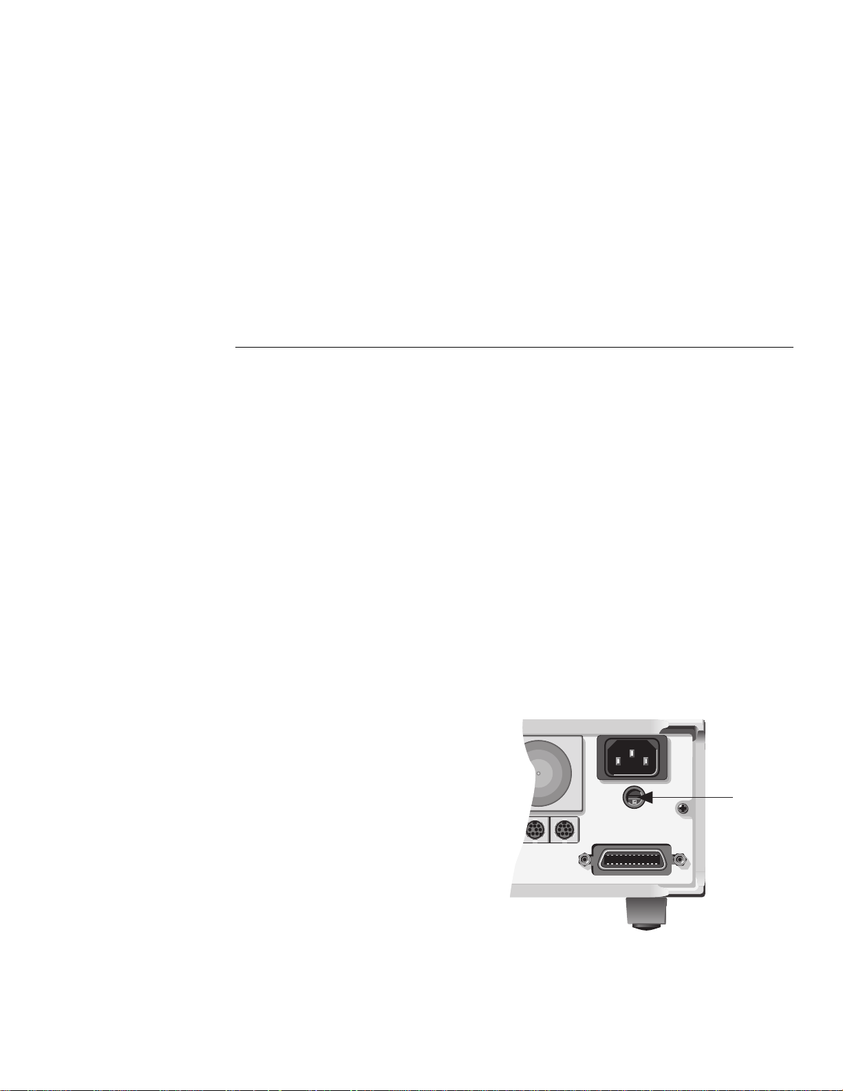
The power line fuse is accessible from the rear panel,
just below the ac power receptacle (see Figure 1-1). Perform the following steps to replace the line fuse:
Figure 1-1
Line fuse location
1-1
Routine Maintenance
NOTE
If the power line fuse continues to
blow, a circuit malfunction exists and
must be corrected. Refer to the troubleshooting section of this manual for
assistance.
Table 1-1
Power line fuse
Keithley
Size Rating
5
×
20mm 250V, ½ A, Slo-Blo FU-71
Part No.
1.3 Current fuse replacement
Each AMPS input (front and rear) has its own current
fuse. When replacing a current fuse, use the type speciÞed in Table 1-2.
CAUTION
To prevent instrument damage, use
only the type speciÞed in Table 1-2.
3. Re-install the fuse carrier.
SENSE
MATH 4W AUTO ARM TRIG SMPL
2001 MULTIMETER
RANGE
AUTO
RANGE
Ω 4 WIRE
350V
PEAK
INPUTS
FR
FRONT/REAR
INPUT
HI
1100V
!
PEAK
LO
500V
PEAK
2A 250V
AMPS
CAL
AMPS
Fuse
Table 1-2
Current fuse
Keithley
Size Rating
5
×
20mm 250V, 2A, Normal-Blo FU-48
Part No.
WARNING
Disconnect the instrument from the
power line and remove all test leads
(front and rear).
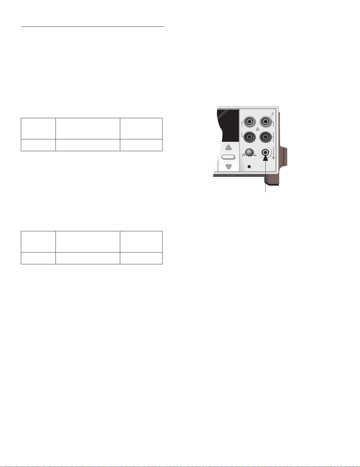
1.3.1 Front AMPS input fuse
The front panel AMPS jack functions as the AMPS input terminal and as the carrier for the AMPS fuse (see
Figure 1-2). Perform the following steps to replace the
fuse:
Figure 1-2
Front AMPS input fuse location
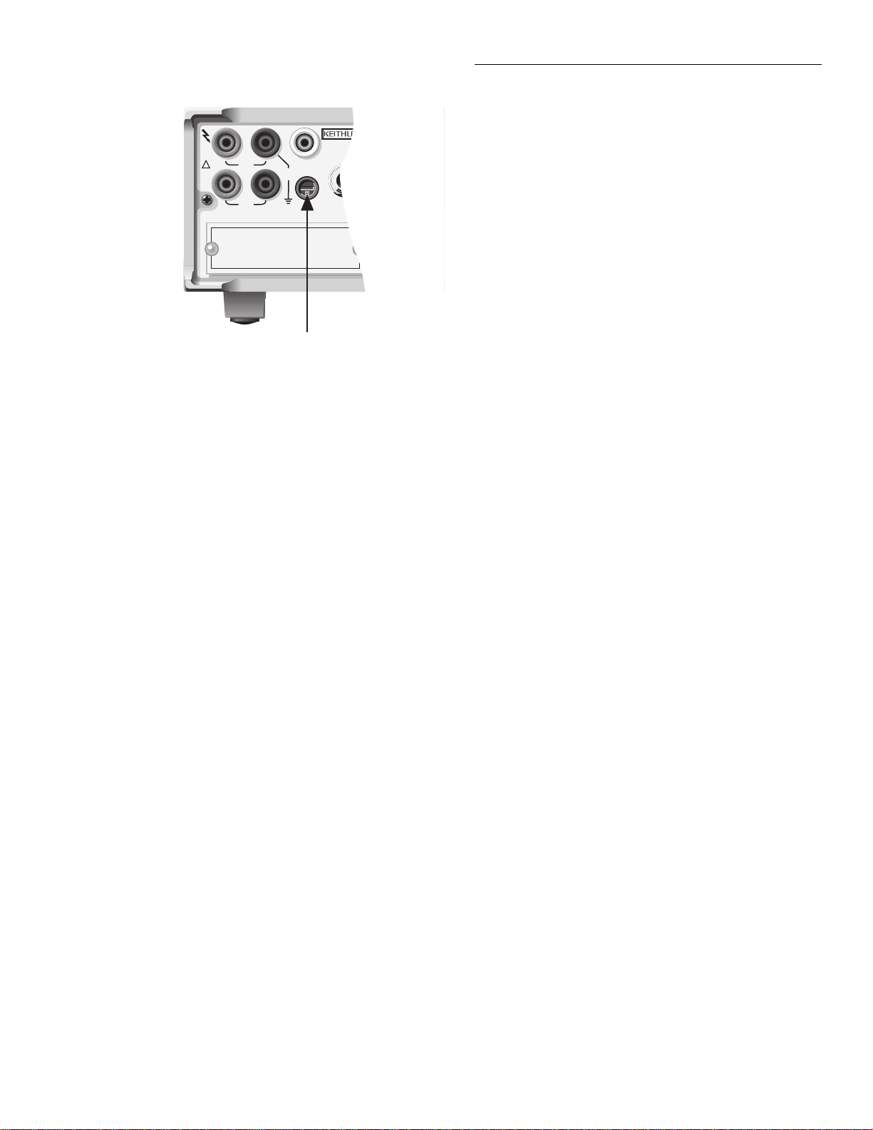
1.3.2 Rear AMPS input fuse
The rear AMPS input fuse is located just below the
AMPS input jack (see Figure 1-3). Perform the following steps to replace the fuse:
1. Insert a bladed screwdriver into the slot of the fuse
carrier.
2. While pushing in, turn the screwdriver counterclockwise until the spring loaded fuse carrier releases from the fuse holder.
3. Pull out the fuse carrier and replace the fuse with
the type speciÞed in Table 1-2.
CAUTION
1. Push in the AMPS input jack and turn counterclockwise until the spring loaded fuse carrier releases from the fuse holder.
2. Pull out the fuse carrier and replace the fuse with
the type speciÞed in Table 1-2.
1-2
To prevent instrument damage, use
only the fuse type speciÞed in Table
1-2.
4. Re-install the fuse carrier.
WARNING:NO INTERNAL OPERATOR SERVICABLE PARTS,SERVIC
WARNING:NO INTERNAL OPERATOR SERVICABLE PARTS,SERVIC
CAUTION:FOR CONTINUED PROTECTION AGAINST FIRE HAZARD,REPLA
CAUTION:FOR CONTINUED PROTECTION AGAINST FIRE HAZARD,REPLA
INPUT
1100V
!
HI LO
PEAK
350V
PEAK
SENSE
Ω 4 WIRE
OPTION SLOT
Figure 1-3
Rear AMPS input fuse location
500V
PEAK
AMPS
2A MAX
AMPS
FUSE
2A, 250V
Amps
Fuse
EXTERNAL
TRIGGER
INPUT
Routine Maintenance
the cover plate.
WARNING
Exercise care when handling the Þlter assembly. The Þlter element is a
metal screen with sharp edges that
could cause injury if not handled
carefully.
The Þlter element is made of a rugged metal screen allowing the use of any type cleaning solution to clean it.
A small metal brush can be used to remove dirt and debris. After cleaning the Þlter, rinse thoroughly with water. Make sure the Þlter assembly is completely dry
before re-installing it.
1.4 Fan filter cleaning
The Þlter for the cooling fan requires periodic cleaning
to maintain proper ventilation. The fan Þlter is accessible from the rear panel. Perform the following steps to
remove the Þlter for cleaning:
1. While facing the rear panel, locate the lower righthand corner of the Þlter cover plate.
2. At this corner, place a thin-bladed screwdriver between the cover plate and the rear panel and gently
pry the Þlter assembly away from the chassis.
The Þlter element is permanently Þxed to the cover
plate. Do not attempt to remove the Þlter element from
1.5 Firmware updates
It is possible that you may receive a Þrmware update
from Keithley to enhance operation and/or Þx ÒbugsÓ.
The Þrmware program for the main microprocessor is
contained in U611 (EPROM). A socket is used on the pc
board for this device to make replacement relatively
easy.
The replacement procedure requires that the case cover
be removed. Also, this surface mount, static-sensitive
device requires special handling. As a result, the Þrmware update should only be performed by qualiÞed
1-3

Routine Maintenance
service personnel. The procedure to replace the Þrmware (U611) is contained in paragraph 3.8.
1-4

2
Troubleshooting
WARNING
The information in this section is intended for qualiÞed service personnel. Some of these procedures may
expose you to hazardous voltages. Do
not perform these hazardous procedures unless you are qualiÞed to do
so.
2.1 Introduction
This section of the manual will assist you in troubleshooting the Model 2001. Included are self-tests, test
procedures, troubleshooting tables and circuit descriptions. It is left to the discretion of the repair technician
to select the appropriate tests and documentation
needed to troubleshoot the instrument.
This section is arranged as follows:
2.2 Repair considerations
ations that should be noted before making any repairs to the Model 2001.
2.3 Power-on test Ñ Describes the tests that are per-
formed on its memory elements every time the
instrument is turned on.
Covers some consider-
2.5 Built-In tests Ñ Provides the procedures to test
and exercise the various circuits on the digital
board, analog board and A/D converter boards.
2.6 Diagnostics Ñ Explains how to use the Diagnos-
tics test mode of the Model 2001. In general, Diagnostics locks-up the instrument in various
states of operation. With the instrument in a static
state, you can then check the state of the various
logic levels on the control registers and signal
trace through the unit.
2.7 R1_STB and R2_STB registers Ñ Provides shift
register bit patterns for the basic measurement
functions and ranges.
2.8 Display board checks Ñ Provides display board
checks that can be made if Front Panel Tests fail.
2.9 Power supply checks Ñ Provides power supply
checks that can be made if the integrity of the
power supply is questioned.
2.10 Documentation Ñ Provides support documen-
tation for the various troubleshooting tests and
procedures. Included is some basic circuit theory
for the display board and power supply, and support documentation for Built-in Test.
2.4 Front panel tests Ñ Provides the procedures to
test the functionality of the front panel keys and
the display.
2.2 Repair considerations
Before making any repairs to the Model 2001, be sure to
read the following considerations.
2-1

Troubleshooting
CAUTION
The PC-boards are built using surface mount techniques and require
specialized equipment and skills for
repair. If you are not equipped and/or
qualiÞed, it is strongly recommended that you send the unit back to the
factory for repairs or limit repairs to
the pc-board replacement level (see
following NOTE).
Without proper equipment and training, you could damage a PC-board
beyond repair.
NOTE
For units that are out of warranty,
completely assembled PC-boards can
be ordered from Keithley to facilitate
repairs.
1. Repairs will require various degrees of disassembly. However, it is recommended that the Front
Panel Tests (paragraph 2.4) and Built-In-Test (paragraph 2-5) be performed prior to any disassembly.
The disassembly instructions for the Model 2001
are contained in Section 3 of this manual.
2. Do not make repairs to surface mount pc-boards
unless equipped and qualiÞed to do so (see previous CAUTION).
3. When working inside the unit and replacing parts,
be sure to adhere to the handling precautions and
cleaning procedures explained in paragraph 3.2.
4. Many CMOS devices are installed in the Model
2001. These static-sensitive devices require special
handling as explained in paragraph 3.3.
5. Anytime a circuit board is removed or a component is replaced, the Model 2001 will have to be
recalibrated.
2.4 Front panel tests
There are two Front Panel Tests; one to test the functionality of the front panel keys and one to test the display. In the event of a test failure, refer to paragraph 2.8
to troubleshoot the display board.
2.4.1 KEYS Test
The KEYS test allows you to check the functionality of
each front panel key. Perform the following steps to
run the KEYS test.
1. Display the MAIN MENU by pressing the MENU
key.
2. Use the or key to place the cursor on TEST
and press ENTER to display the SELF-TEST
MENU.
3. Place the cursor on FRONT-PANEL-TESTS and
press ENTER to display the following menu:
FRONT PANEL TESTS
KEYS DISPLAY-PATTERNS
4. Place the cursor on KEYS and press ENTER to start
the test. When a key is pressed, the label name for
that key will be displayed to indicate that it is functioning properly. When the key is released, the
message ÒNo keys pressedÓ is displayed.
5. Pressing EXIT tests the EXIT key. However, the second consecutive press of EXIT aborts the test and
returns the instrument to the SELF-TEST MENU.
Keep pressing EXIT to back out of the menu structure.
2.4.2 DISPLAY PATTERNS Test
The display test allows you to verify that each pixel
and annunciator in the vacuum ßuorescent display is
working properly. Perform the following steps to run
the display test:
2.3 Power-on test
During the power-on sequence, the Model 2001 will
perform a checksum test on its EPROM (U611 and
U618) and test its RAM (U608, U609, and U610. If one
of these tests fail the instrument will lock up.
2-2
1. Display the MAIN MENU by pressing the MENU
key.
2. Use the or key to place the cursor on TEST
and press ENTER to display the SELF-TEST
MENU.
3. Place the cursor on FRONT-PANEL-TESTS and
press ENTER to display the following menu:

Troubleshooting
FRONT PANEL TESTS
KEYS DISPLAY-PATTERNS
4. Place the cursor on DISPLAY-PATTERNS and
press ENTER to start the display test. There are Þve
parts to the display test. Each time a front panel
key (except EXIT) is pressed, the next part of the
test sequence is selected. The Þve parts of the test
sequence are as follows:
A. Checkerboard pattern (alternate pixels on) and
all annunciators.
B. Checkerboard pattern and the annunciators
that are on during normal operation.
C. Horizontal lines (pixels) of the Þrst digit are se-
quenced.
D. Vertical lines (pixels) of the Þrst digit are se-
quenced.
E. Each digit (and adjacent annunciator) is se-
quenced. All the pixels of the selected digit are
on.
5. When Þnished, abort the display test by pressing
EXIT. The instrument returns to the SELF-TEST
MENU. Keep pressing EXIT to back out of the
menu structure.
Table 2-1
Built-in-test summary
Test Circuit tested/exercised
100 Series
100.1
101 Series
101.1
102 Series
102.1
103 Series
103.1 - 103.4
103.5
104 Series
104.1
104.2
105 Series
105.1 - 105.6
105.7
Memory:
EPROM
Memory:
RAM
Memory:
2
E
PROM
Digital I/O:
Digital Output
Digital Input
IEEE-488 Bus:
Handshake
Data
Triggers:
System Trigger Bus
External Trigger /Voltmeter Complete
105.8
Group Execute Trigger
(GET)
105.11 - 105.18
Trigger Shorts
2.5 Built-in test
BUILT-IN TEST is used to test and exercise various circuits and components on the digital board, analog
board and A/D converter board. The Built-In Tests are
listed in Table 2-1. Many of the tests are actual pass/fail
type tests, while others are circuit exercises that are
used for subsequent tests. Each Built-In Test can be run
manually. After a test is manually run, operation is
ÒfrozenÓ to allow the technician to troubleshoot the circuit. Troubleshooting documentation for each Built-In
Test is provided in paragraph 2.10.3.
200 Series
200.1
200.2
200.3
200.4
200.5
200.6
200.7
201 Series
201.1
201.2
201.3
300 Series
300.1
300.2
300.3
301 Series
301.1
301.2
A/D Converter:
A/D Zero
A/D Noise
FAST Circuit
x10 Line Cycle Integration
x0.1 Line Cycle Integration
x0.02 Line Cycle Integration
x0.01 Line Cycle Integration
Calibration:
Test Cal Zero
7V Reference
1.75V Reference
A/D Multiplexer (MUX),
A/D Buffer:
7V Reference, x1.5 Gain
1.75V Reference, x5 Gain
0V Reference, x50 Gain
Input Buffer:
Front End (FE) Zero
Divide by 100
2-3

Troubleshooting
Table 2-1 (cont.)
Built-in-test summary
Test Circuit tested/exercised
302 Series
302.1
Ohms:
Zero Reference Measurement (for next test)
302.2
Open Circuit Ohms and
Ohms Protection
303 Series
303.1
Input Path:
Zero Reference Measurement (for next test)
303.2
Open Circuit Ohms and
Ohms Protection
303.3
Front End (FE) Zero Protection
304 Series
304.1
Ohms Sources:
Zero Reference Measurement (for tests 304.2 -
304.7)
304.2
0.98mA and 9.2mA Ohms
Sources
304.3
89
µ
A and 0.98mA Ohms
Sources
304.4
7
µ
A and 89
µ
A Ohms
Sources
304.5
770nA and 7
µ
A Ohms
Sources
304.6
70nA and 770nA Ohms
Sources
304.7
4.4nA and 770nA Ohms
Sources
Table 2-1 (cont.)
Built-in-test summary
Test Circuit tested/exercised
308 Series
308.1
4-Digit Mode:
A/D MUX 4-Digit Signal
Path
308.2
A/D MUX 4-Digit Zero
Path
309 Series
309.1
309.2
309.3
309.4
Amps:
A Range
200
µ
2mA Range
20mA Range
Reference Measurement
(for tests 309.5 and 309.6)
309.5
309.6
310 Series
310.1
400 Series
200mA Range
2A Range
Protection:
Amps Protection
Digital-to-Analog Converter
(DAC):
400.1
400.2
400.3
400.4
400.5
401 Series
401.1
402 Series
402.1
-4.21V Output
-2.08V Output
-0.001V Output
+2.25V Output
+4.33V Output
Signal Switching:
Zero Cal Switch
Signal Switching:
Frequency Switch
305 Series
305.1
305.2
306 Series
306.1
307 Series
307.1
307.2
307.3
2-4
Input Divider:
Zero Reference Measurement (for next test)
Divide by 100
Switching:
Ohms Cal Switch
Cal Divider:
Zero Reference Measurement (for next test)
A/D MUX /10
A/D MUX /Buffer (x-0.5)
403 Series
403.1
404 Series
404.1
404.2
404.3
404.4
404.5
Signal Switching:
Ground Switch
Absolute Value (x1 Gain):
-Full Scale DAC Output
-Half Scale DAC Output
Zero DAC Output
+Half Scale DAC Output
+Full Scale DAC Output

Troubleshooting
Table 2-1 (cont.)
Built-in-test summary
Test Circuit tested/exercised
405 Series
405.1
405.2
405.3
405.4
405.5
405.6
405.7
405.8
406 Series
406.1
406.2
406.3
406.4
406.5
406.6
407 Series
407.1
407.2
407.3
408 Series
408.1
408.2
408.3
408.4
408.5
408.6
Absolute Value (x10 Gain):
Gain Comparison (Large
+DAC Output)
Gain Comparison (Large
+DAC Output)
Gain Comparison (Small
+DAC Output)
Gain Comparison (Small
+DAC Output)
Gain Comparison (Small
-DAC Output)
Gain Comparison (Small
-DAC Output)
Gain Comparison (Large
-DAC Output)
Gain Comparison (Large
-DAC Output)
Test Buffer:
Measure DAC Output (for
test 406.6)
Test Buffer Output (-1.13V)
Read Test Buffer (for test
406.6)
Read DAC Output (for test
406.6)
Test Buffer Output (-0.01V)
Voltage Comparisons
Front End:
2V Range
200V Range
750V Range
/200 Correction Factor:
Circuit Setup (for next test)
Signal Stored (for next test)
Setup (for test 408.5) and
Measurement (for test
408.6)
Same as Test 408.3 but no
measurement.
Signal Stored (for next test)
Signal Comparisons
Table 2-1 (cont.)
Built-in-test summary
Test Circuit tested/exercised
409 Series
409.1
409.2
409.3
409.4
409.5
409.6
410 Series
410.1
411 Series
411.1
411.2
412 Series
412.1
/750 Correction Factor:
Circuit Setup (for next test)
Signal Stored (for next test)
Setup (for test 409.5) and
Measurement (for test
409.6)
Same as Test 409.3 but no
measurement.
Signal Stored (for next test)
Signal Comparisons
Converter:
TRMS Converter
Filters:
TRMS Filter
Variable Gain AmpliÞer
Filter
Switching:
AC Amps Switch
Typical Way To Use BUILT-IN-TEST
1. Run the AUTOMATIC Built-In-Test as explained in
paragraph 2.5.1 and note the Þrst (lowest numbered) test that has failed. You should always address the lowest numbered test failure Þrst because
that failure could cause subsequent tests to fail.
2. Familiarize yourself with the failed circuit. Documentation for the Built-In Tests are provided in
paragraph 2.10.3. Be sure to read the documentation for the complete series. For example, if test
200.4 fails, read the documentation for all 200 series tests (200.1 through 200.7). Note that the documentation directs you to the appropriate
schematic(s) for the circuit.
3. Manually run the test that failed as explained in
paragraph 2.5.2. Keep in mind that many of the
pass/fail type tests require that one or more circuit
exercise tests be run Þrst. Using the manual step
looping mode will ÒfreezeÓ instrument operation
after a test is run.
4. After manually running the test, use the test documentation and your troubleshooting expertise to
locate the problem.
2-5

Troubleshooting
5. After repairing the instrument, start again at step 1
to check the integrity of the repair and to see if
there are any other failures.
2.5.1 AUTOMATIC Testing
1. Display the MAIN MENU by pressing the MENU
key.
2. Use the or key to place the cursor on TEST
and press ENTER to display the SELF-TEST
MENU.
3. Place the cursor on BUILT-IN-TEST and press ENTER to display the following menu:
BUILT-IN TEST
AUTOMATIC MANUAL
4. Place the cursor on AUTOMATIC and press ENTER. The following prompt is displayed:
CONTINUOUS REPEAT?
NO YES
The star (*) is only displayed if a failure occurs.
7. If all the tests passed (no star displayed), use the
EXIT key to back out of the menu structure. Otherwise, press ENTER to display the test number of
the Þrst failure. You can display any additional failures by using the and keys. With a failed test
displayed, pressing the INFO key provides an abbreviated description of the failure. Paragraph 2.10
provides detailed documentation for troubleshooting the defective circuit. When Þnished, use EXIT
to back out of the menu structure.
2.5.2 MANUAL Testing
1. Display the MAIN MENU by pressing the MENU
key.
2. Use the or key to place the cursor on TEST
and press ENTER to display the SELF-TEST
MENU.
3. Place the cursor on BUILT-IN-TEST and press ENTER to display the following menu:
In the non-repeat mode (NO), the testing process
stops after all tests have been performed one time.
In the continuous repeat mode (YES), the testing
process loops around and repeats indeÞnitely until
the EXIT key is pressed to stop the tests.
5. Place the cursor on the desired repeat mode selection (NO or YES) and press ENTER to start the testing process. The instrument displays the number
of the test being run. An ÒAÓ on the display indicates that the tests are being run automatically in
the non-repeat mode. An ÒACÓ indicates that the
tests are being run automatically in the continuous
repeat mode. If a failure occurs, a star (*) appears at
the right hand end of the display and remains on
for the remainder of the tests.
6. If the non-repeat mode is selected, the testing process automatically stops when all the tests have
been performed. If the continuous repeat mode is
selected, you will have to manually stop the testing
process by pressing EXIT. When EXIT is pressed,
all the tests in a series already started will be allowed to Þnish.
When the testing process stops, the following message is displayed:
All tests complete *
Press ENTER to review or EXIT
BUILT-IN TEST
AUTOMATIC MANUAL
4. Place the cursor on MANUAL and press ENTER to
display the currently selected test series number.
Test number: 100
This test number indicates that the 100 series tests
can be performed. In this case there is only one test;
test 100.1.
5. Use the or to display the desired test series
number. For example, if you wish to run test 200.5,
display the series 200 test number.
Test number: 200
6. With the desired test series number displayed,
press ENTER. The following menu displayed:
SELECT LOOPING
SINGLE CONTINUOUS STEP
7. Place the cursor on the desired looping selection
and press ENTER.
A. SINGLE Looping performs all the tests in the
speciÞed series. The instrument displays the
number of the test being run, and an ÒMÓ is dis-
2-6

Troubleshooting
played to indicate that the tests are being run in
the manual single looping mode. If a failure occurs, a star (*) appears at the right hand end of
the display and remains on for the remainder
of the tests in the series. This testing process automatically stops after the last test in the series
is completed. This test process can also be
stopped by pressing EXIT. When EXIT is
pressed, any test in process will be allowed to
Þnish before aborting the testing process.
B. CONTINUOUS looping continuously repeats
all the tests in the speciÞed series until the testing process is manually stopped. During testing, the ÒMCÓ message is displayed to indicate
that tests are being run in the manual continuous looping mode. If a failure occurs, a star (*)
appears at the right hand end of the display
and remains on for the remainder of the tests in
the series. This test process can be stopped by
pressing EXIT. When EXIT is pressed, any test
in process will be allowed to Þnish before
aborting the testing process.
C. STEP looping is used to perform one test at a
time. Each press of the ENTER key performs
the displayed test. The ÒMSÓ message is displayed to indicate that tests are being run in the
manual step looping mode. If a failure occurs,
a star (*) appears at the right hand end of the
display and remains on for the remainder of
the tests in the series. The instrument automatically aborts the testing process after the last
test in the series is run. If you do not wish to
run all the tests in the series, simply press EXIT
after the desired test is run.
8. After the testing process is stopped, the following
message is displayed:
All tests complete *
Press ENTER to review or EXIT
The star (*) is only displayed if a failure occurs.
9. In the event of no test failures, press any key to return to the BUILT-IN TEST menu. If you wish to
run more tests, repeat steps 4 through 8.
In the event of a failure, press ENTER to display
the Þrst test that failed. Other test failures can be
displayed by using the and keys. The INFO
key can be used to provide a brief summary of each
displayed test failure. Paragraph 2.10.3 provides
detailed documentation for troubleshooting the
defective circuit. When Þnished, press EXIT to re-
turn to the BUILT-IN TEST menu. If you wish to
run more tests, repeat steps 4 through 8.
10. When Þnished with BUILT-IN TEST, use the EXIT
key to back out of the menu structure.
2.6 Diagnostics
The Model 2001 has diagnostic test modes which allow
you to ÒfreezeÓ instrument operation to allow you to
check logic levels on the DC_STB control registers
(U303, U300, U800 and U801). The known bit pattern at
these registers can then be used for signal tracing
through the unit. Table 2-10 provides a brief description of each register bit.
Perform the following steps to use DIAGNOSTICS:
1. Select the desired function and range to be
checked. Note that there are no range selections for
FREQ and TEMP.
2. Display the MAIN MENU by pressing the MENU
key.
3. Using the or key to place the cursor on TEST
and press ENTER to display the SELF-TEST
MENU.
4. Place the cursor on DIAGNOSTICS and press ENTER. The Þrst diagnostic test mode (Signal Phase
or Ohms Sense High) is selected (displayed).
5. Perform the following steps to determine the bit
pattern at the control registers:
A. Refer to one of the following DIAGNOSTIC
Test Modes tables to determine the bit pattern
designator (A through X) for the selected function/range:
Table 2-2 Ñ All functions except
Table 2-3 Ñ
Table 2-4 Ñ
ranges
B. Once the bit pattern designator is determined,
use Table 2-5 to determine the logic state of
each register bit.
Example: Assume the 20VDC range is selected
and the instrument is in the ÒSignal PhaseÓ of
DIAGNOSTICS. From Table 2-2, the bit pattern
designator is C. Table 2-5 provides the logic
states for bit pattern C.
6. Use the cursor keys to select the other diagnostic
test modes. The key scrolls forward through the
Ω
4 function; 20
Ω
4 function, 2k
Ω
and 200
Ω
, 20k
Ω
4
Ω
Ω
and 200k
ranges
Ω
2-7
Troubleshooting
test modes and the key scrolls backward.
Again, use the appropriate tables to determine the
bit pattern at the control registers.
7. When Þnished, press EXIT three times to back out
Table 2-2
DIAGNOSTICS test modes (all functions except Ω4)
Test mode Selected function Selected range Bit pattern
Signal Phase DCV 200mV
ACV, ACI and FREQ All E
DCI All F
Ω220Ω, 200Ω
TEMP RTD (open input) Ñ H
of the menu structure and return to the normal
measurement mode of operation.
8. If you wish to check another function/range, repeat steps 1 through 7.
designator*
A
2V, 200V
20V
1000V
B
C
D
G
2kΩ-200MΩ
1GΩ
H
I
TEMP TC Ñ B
7V div by 1 * 1 All (except Ω4) All J
7V div by 1 * 1.5 All (except Ω4) All K
2V div by 1 * 5 All (except Ω4) All L
0V div by 1 * 1 All (except Ω4) All M
0V div by 1 * 5 All (except Ω4) All N
0V div by 1 * 50 All (except Ω4) All O
0V div by 1 * 1.5 All (except Ω4) All P
FE zero for 200mV All (except Ω4) All Q
FE zero for 2V All (except Ω4) All R
*Bit patterns are provided in Table 2-5.
2-8

Troubleshooting
Table 2-3
DIAGNOSTICS test modes (
and 200
Ω
ranges)
Ω
4 function; 20
Test mode Bit pattern
designator*
Ohms sense high G
7V div by 1 * 1 P
7V div by 1 * 1.5 Q
2V div by 1 * 5 R
0V div by 1 * 1 S
0V div by 1 * 5 T
0V div by 1 * 50 U
0V div by 1 * 1.5 V
Ohms sense minus W
FE zero for 2V X
*See Table 2-5 for bit patterns.
Table 2-4
Ω
DIAGNOSTICS test modes (
thru 200k
Ω
ranges)
Ω
4 function; 2k
Ω
Test mode Bit pattern
designator*
Ohms sense high H
7V div by 1 * 1 P
7V div by 1 * 1.5 Q
2V div by 1 * 5 R
0V div by 1 * 1 S
0V div by 1 * 5 T
0V div by 1 * 50 U
0V div by 1 * 1.5 V
FE zero for 200mV W
Ohms sense minus X
*See Table 2-5 for bit patterns.
2-9

Troubleshooting
Registers
U303 U300 U800 U801
Q8 Q7 Q6 Q5 Q4 Q3 Q2 Q1 Q8 Q7 Q6 Q5 Q4 Q3 Q2 Q1 Q8 Q7 Q6 Q5 Q4 Q3 Q2 Q1 Q8 Q7 Q6 Q5 Q4 Q3 Q2 Q1
D XX111110 01110111 01010101 01000100
E XX101101 01111111 01010101 01000100
F XX011011 01111111 01010101 01000100
B XX111101 01110111 01010101 01000100
C XX111111 00011110 01010101 01000100
A XX111011 01110111 01010101 01000100
Bit
DIAGNOSTICS bit patterns (DC_STB registers)
Table 2-5
pattern
G XX111011 01110111 11010101 01000100
H XX111101 01110111 11010101 01000100
I XX111110 01110111 11010101 01000100
J XX111110 01111011 01101010 10000100
K XX111111 01011011 01010101 01000100
L XX110101 01111111 01101010 10000100
M XX111110 00111111 01010101 01000100
N XX111101 00111111 01101010 10000100
O XX111011 00111111 01010101 01000100
P XX111111 00011111 01101010 10000100
Q XX111011 11110101 01010101 01000100
R XX111101 11110101 01101010 10000100
S 00111110 00111111 01101010 01010101
T 00111101 00111111 01010101 10101110
U 00111011 00111111 01101010 01010101
V 00111110 00011111 01010101 10101110
W 00111011 11110100 01101010 01010101
X 00111101 11110101 01010101 10101110
2-10

Troubleshooting
2.7 R1_STB and R2_STB shift registers
Table 2-6 and Table 2-7 are provided to allow you to
check logic levels on the R1_STB and R2_STB shift registers (U302, U305, U307, U501, U530, U500 and U505)
for each basic measurement function (DCV, ACV, DCI,
ACI,
Ω
2 and
Ω
4) and range. The known bit pattern at
these registers can then be used for signal tracing
through the unit. Tables 2-11 and Table 2-12provide a
brief description of each register bit.
To use these tables, simply place the instrument in the
designated function and range and check the output of
the shift registers for the indicated bit pattern. The bit
patterns in these tables assume the following conditions:
NPLC > 0.01
AC Type = RMS or Average
Offset Compensated Ohms = Off
Current Measurement Mode = Normal (No In-Circuit I)
2-11

Troubleshooting
10011010
11011010
11011010
11011010
11011010
11011010
11011010
11011010
11011010
11011010
11011010
11011010
10011000
10011001
10011010
10011011
00011011
10011011
10011011
11011100
11011101
11011110
11011111
11110100
11000000
U302 U305 U307
01111111
01111111
Q8 Q7 Q6 Q5 Q4 Q3 Q2 Q1 Q8 Q7 Q6 Q5 Q4 Q3 Q2 Q1 Q8 Q7 Q6 Q5 Q4 Q3 Q2 Q1
200V, 1000V
DCV 200mV-20V
Function Range Registers
Bit patterns for R1_STB registers
Table 2-6
ACV All 01111111 11000000 11111010
11000000
01111010
DCI 200µA
11000000
11000000
01110110
01101110
2mA
20mA
11000000
11000000
01011110
00111111
200mA
2A
11000000
01111010
ACI 200µA
11000000
11000000
01110110
01101110
2mA
20mA
11000000
11000000
01011110
00111110
200mA
2A
11110110
01111111
Ω220Ω
11110110
01111111
200Ω, 2kΩ
11110110
01111111
20kΩ
11110110
01111111
200kΩ
11111110
01111111
2MΩ
11111110
01111111
20MΩ
01111110
01111111
200MΩ, 1GΩ
10110010
01111111
Ω420Ω
10110010
01111111
200Ω, 2kΩ
10110010
01111111
20kΩ
10110010
01111111
200kΩ
2-12

Table 2-7
Bit patterns for R2_STB registers
Registers
U501 U530
Function Range
DCV All 0110101000000000
ACV 200mV
2V
20V
200V
750V
DCI All 0110101000000000
ACI All 0110000110000000
Ω2, Ω4 All 0110101000000000
Q8 Q7 Q6 Q5 Q4 Q3 Q2 Q1 Q8 Q7 Q6 Q5 Q4 Q3 Q2 Q1
01110001
01110001
01110001
01110001
01110001
10000000
10000000
10000000
10000000
10000000
Registers
Troubleshooting
U500 U505
Range Range
DCV All 10100011 00000111
ACV 200mV
2V
20V
200V
750V
DCI All 10100111 00011111
ACI All 11101111 01001111
Ω2, Ω4 All 10100011 00000111
Q8 Q7 Q6 Q5 Q4 Q3 Q2 Q1 Q8 Q7 Q6 Q5 Q4 Q3 Q2 Q1
11101101
11101001
11101110
11101110
11101010
10011111
10111111
00011110
00011110
00011110
2-13

Troubleshooting
2.8 Display board checks
If the FRONT PANEL TESTS (paragraph 2.4) indicate
that there is a problem on the display board, use Table
2-8.
Circuit theory for the display is provided in paragraph
2.9.1.
Table 2-8
Display board checks
Step Item/component Required condition Remarks
1 FRONT PANEL TESTS Verify that all pixels operate Use SELF-TEST MENU selection
2 P1033, pins 4, 6, 14 and 16 5VAC, ±0.3VAC VFD Þlament
2.9 Power supply checks
Power supply problems can be checked out using Table 2-9.
3 P1033, pin 5 +5V, ±5% Digital +5V supply
4 P1033, pin 9 +60V, ±10% VFD +60V supply
5 P1033, pin 12 Goes low brießy on power-up,
then goes high
6 P1033, pin 2 4MHz square wave Controller 4MHz clock
7 P1033, pin 8 Pulse train every 1msec Control from main processor
8 P1033, pin 10 Brief pulse train when front
panel key is pressed
Microcontroller RESET line
Key down data sent to main processor.
2-14

Table 2-9
Power supply checks
Step Item/component Required condition Remarks
1 F100 line fuse Check continuity Remove to check
Troubleshooting
2 Line power Plugged into live receptacle,
power on
3 U108, pin 3 +5V, ±5% Reference to Common 3
4 U107, pin 3 +15V, ±0.75V Reference to COM
5 U102, pin 3 -15V, ±0.75V Reference to COM
6 CR109, +BS +34V to +38V Reference to Common 3
7 CR110, -BS -34V to -38V Reference to Common 3
8 U103, pin 3 ~+18V Reference to Isolated Common
9 U103, pin 2 +8V Reference to Isolated Common
10 U619, +5VC +5V, ±5% Reference to Digital Common
11 U629, pin 3` +5V, ±5% Reference to Digital Common
2.10 Documentation
The following information is provided to support the
troubleshooting tests and procedures previously covered in this section of the manual. Figure 2-1 provides
an overall block diagram of the Model 2001 showing
the major circuit groups. Most circuits in the Model
2001 are tested and/or exercised by Built-in Test. A
short description for each of these tests explains how
that particular circuit operates. The display board and
the power supply are not tested by Built-in Test. Thus,
some basic theory is provided for these circuits in paragraphs 2.10.1 and 2.10.2.
Check for correct power up
sequence
2-15
Troubleshooting
Digital
55 Vdc 5 Vdc 5.5 Vac
Front
Panel
Controller
Front Panel Reset
Front Panel Clock
Front Panel Data Out
Front Panel Data In
68302
IEEE
Data Out
IEEE
Data
Trigger
(DMA)
In (ISR)
Software
Delay
IEEE-488 Bus
GPIB
56
Digital I/O
Trigger
F/R Status
DC SIG/REF
Signal
DC Input
ADC Data In
O
PTOIS
ADC Data In
DC/MUX FETS
Conditioning
CLK
ADC
CLK
TRMS,
DATA
DATA
AVE,
Amps
O
STB
PK
STB
TRG
Control
Data Out
FREQ Out
Signal
AC Input
Hardware
Trigger
AC FETS
(w/freq)
Conditioning
Select
Trigger
Logic
Scanner Control Out
Option
Scanner
FREQ In
External Trigger,
Power Supply
Meter Complete
Trigger Bus
Figure 2-1
Model 2001 overall block diagram
2-16
Amps
Sense HI
Sense LO
Scanner Output
Scanner
Inputs
Input HI
Input LO

Troubleshooting
2.10.1 Display board circuit theory
The following information provides some basic circuit
theory that can be used as an aide to troubleshoot the
display and keyboard.
Display microcontroller
U902 is the display microcontroller that controls the
VFD (vacuum ßuorescent display) and interprets key
data. The microcontroller has four peripheral I/O
ports that are used for the various control and read
functions.
Display data is serially transmitted to the microcontroller from the digital board via the TXB line to the microcontroller PD0 terminal. In a similar manner, key
data is serially sent back to the digital board through
the RXB line via PD1. The 4MHz clock for the microcontroller is generated on the digital board.
Vacuum fluorescent display
2.10.2 Power supply circuit theory
The following information provides some basic circuit
theory that can be used as an aide to troubleshoot the
power supply.
Pre-regulator circuit
The pre-regulator circuit regulates power to the transformer. When power is applied to the instrument, a
power transformer secondary voltage (pins 12 and 13)
is rectiÞed (CR622), doubled (C624, C630, CR624 and
CR625) and applied to U619 which is a +5V regulator.
This +5V (+5VC) is used for the pre-regulator circuit.
The pre-regulator circuit monitors the voltage level on
C611 using an integrator (U627). The voltage on C611
(typically around 7.5V) is divided by three through
R712 and R713 and applied to the inverting input (pin
2) of the integrator. The +5V (+5VC) is divided by two
through R706 and R708. This 2.5V reference is applied
to the non-inverting input (pin 3) of the integrator.
DS901 is the VFD (vacuum ßuorescent display) module, which can display up to 49 characters. Each char-
acter is organized as a 5 × 7 matrix of dots or pixels and
includes a long under-bar segment to act as a cursor.
The display uses a common multiplexing scheme with
each character refreshed in sequence. U903 and U904
are the grid drivers, while U901 and U905 are the dot
drivers. Note that dot driver and grid driver data is serially transmitted from the microcontroller (PD3 and
PC1).
The VFD requires both +60VDC and 5VAC for the Þlaments. These VFD voltages are supplied by U625,
which is located on the digital board.
Key matrix
The front panel keys (S901-S931) are organized into a
row-column matrix to minimize the number of microcontroller peripheral lines required to read the keyboard. A key is read by strobing the columns and
reading all rows for each strobed column. Key down
data is interpreted by the display microcontroller and
sent back to the main microprocessor using proprietary
encoding schemes.
When the voltage on the inverting input of the integrator is less than the 2.5V reference on the non-inverting
input, the integrator output ramps in the positive direction. This positive ramp turns on Q608 which pulls
the CONT line low to digital common. With CONT
connected to common, current ßows through the photodiode of U100 and generates a positive voltage at the
gate of FET Q528. As Q528 turns on, the 470Ω resistor
(R100) becomes shunted and results in less effective resistance to the transformer. The resultant increase in
current (power) will increase the voltage on C611.
Conversely, when the voltage on the inverting input of
the integrator is more than the 2.5V reference, the integrator output ramps in the negative direction and begins to turn Q608 off. This will decrease current
through U100, decrease the positive voltage on Q528
and thus, increase the effective resistance to the transformer. The resultant decrease in current (power) will
decrease the voltage of C611.
This constant regulation of effective resistance in series
with the transformer regulates the power delivered to
the instrument.
2-17

Troubleshooting
Line voltage (110V/220V) selection circuit
This circuit automatically selects the proper power line
voltage setting for the instrument. The line selection
circuit derives its power from the AC1 and AC2 lines
on the primary side of the transformer. RectiÞer CR101
applies approximately +18V to regulator U103. The
output of U103 provides the +8V for the line voltage selection circuit and the HI/LO voltage control circuit.
U106 is a comparator that has a +4V reference (via voltage divider R125 and R126) applied to its non-inverting input. The inverting input monitors the voltage on
C111. When the voltage at the inverting input is greater
than 4V, the output of U106 goes low and turns on FET
Q103. With Q103 on, +8V will be applied to the
+RELAY1 line which energizes relay K101 to select the
110V setting. Conversely, when the voltage at the inverting input is less than 4V, the output of U106 goes
high and turns off Q103. With Q103 off, the +8V is removed from K101 and thus, the line voltage setting defaults to 220V.
The AC power line is tied to C111 through CR104, R227
and R114 via control line ACL. When the AC power
line voltage is less than approximately 135VAC, sufÞcient charge remains on C111 to keep the inverting input of U106 above 4V to ultimately energize K101
(110V setting). When the AC power line voltage is
greater than approximately 18VAC, charge will be
pulled from C111 dropping the voltage at the inverting
input of the comparator to less than 4V. This will de-energize K101 (220V setting).
HI/LO voltage control circuit
This circuit automatically selects the appropriate HI/
LO setting for the available power line voltage. During
power-up, the line voltage is rectiÞed (CR100), divided
(R103 and R105, or R102 and R105) and applied to the
base of Q101.
If the voltage level at the base of Q101 is high (above
zener VR101), the transistor will turn on and apply
power to the ISO1+ and ISO1- lines. With power applied to ISO1+ and ISO1-, U105 will turn on and allow
Q105 to be forward biased. With U105 and Q105 on,
TRIG of U110 will be pulled low and allow its output
(OUT) to latch at +8V which will turn on FET Q102.
With Q102 on, the -RELAY2 line will be connected to
common, and thus energize K100 (HI setting).
If the power line voltage decreases to a low level, U105
will turn off, but the output of U110 will remain latched
at +8V. However, the LOW line will be driven low turning on U109. With U109 and Q106 on, +8V will be applied to THR of U110 forcing its output (OUT) to reset
to low. With the gate of Q102 low, the FET will turn off
and open the relay coil circuit for K100 (LO setting).
The LOW line is controlled by comparator U628. The
inverting input of the comparator is connected to the
2.5V reference. The non-inverting input monitors (via
divider R709 and R711) C611. As previously explained,
the typical power line voltage level will apply around
7.5V to C611. However, if the line voltage decreases
such that the voltage on C611 becomes less than 6V, the
voltage level on the non-inverting input of the comparator will drop below 2.5V causing its output (LOW
line) to go low.
2.10.3 Built-in test documentation
The information in this paragraph provides documentation for each Built-In Test. Paragraph 2.5 explains
how to use the Built-In Test.
The following documentation is provided for each
Built-In Test:
1. Test Type Ñ Some tests are pass/fail type tests
while others are circuit exercises that are used for
subsequent tests.
2. Failure Analysis Ñ For pass/fail type tests, a summary is provided to explain the cause of the failure.
3. Description Ñ Provides a description of the circuit
being tested.
4. Schematic Reference Ñ Directs you to the appropriate schematic(s) for the circuit being tested.
5. High Suspect Components Ñ When appropriate,
possible defective components and/or circuits are
listed. It is left to the expertise of the repair technician to pin-point the problem.
6. Shift Registers Ñ For tests starting with 200.1, the
logic states for the control shift registers are provided. After one of these tests is manually run, you
can check the registers for the correct logic levels.
Tables 2-10 through 2-12 provide functional descriptions for the register bits.
7. Multiplexer Ñ For manually run tests that exercise
the multiplexer (U511), you can use Table 2-13 to
check the logic levels on its control lines.
2-18

Table 2-10
DC_STB control registers
Register Bit Pin Control Description
Troubleshooting
U801 Q1
Q2
Q3
Q4
Q5
Q6
Q7
Q8
U800 Q1
Q2
Q3
Q4
Q5
Q6
Q7
Q8
U300 Q1
Q2
Q3
Q4
Q5
Q6
Q7
Q8
4
5
6
7
14
13
12
11
4
5
6
7
14
13
12
11
4
5
6
7
14
13
12
11
FAST
LST_PH
FREQ_EN
I3, FREQ_LOAD
I4
I5
I6
I7
I8
I9
I10
I11
I12
I13
OHMCA
OHMCB
BUF, /BUF
VLO2, BSCOM
/REF
//1
/CAL
//2
/ZERO
FE ZERO, ONE SHOT
1 = FAST integration on A/D converter (ADC).
1 = Normal ADC operation.
1 = Normal ADC operation.
1 = Normal ADC operation.
Set ADC conversion rate (LSB).
Set ADC conversion rate.
Set ADC conversion rate.
Set ADC conversion rate.
Set ADC conversion rate.
Set ADC conversion rate.
Set ADC conversion rate.
Set ADC conversion rate.
Set ADC conversion rate.
Set ADC conversion rate (MSB).
Select Ohms Cal on U325 (LSB).
Select Ohms Cal on U325 (MSB).
1 = Q306 on and Q304 off.
0 = -8VF to VLO2, 1 = -8VF to BSCOM.
0 = 7V ref to A/D Buffer (via U317).
0 = Input Buffer to A/D Buffer (Q308 and Q313
on).
0 = Cal Divider to A/D Buffer (via U319).
0 = -0.5 or 1.5 gain (via U319).
0 = Zero to A/D Buffer (via U319).
1 = Q527 and Q539 on, 0 = ONE SHOT (via U334)
for PRECHARGE (Q538 on).
U303 Q1
Q2
Q3
Q4
Q5
Q6
Q7
Q8
4
5
6
7
14
13
12
11
/X1
/X5
/X50
/2VREF
/AC
/DCA
nc
nc
0 = x1 A/D Buffer; U318 (/X1) closed.
0 = x5 A/D Buffer; U318 (/X5) closed.
0 = x50 A/D Buffer; U318 (/X50) closed.
0 = 1.75V ref to A/D Buffer (via U318).
0 = ACV/A to A/D Buffer (via U320).
0 = DCA to A/D Buffer (via U320).
x
x
2-19

Troubleshooting
Table 2-11
R1_STB control registers
Register Bit Pin Control Description
U307 Q1
Q2
Q3
Q4
Q5
Q6
Q7
Q8
U305 Q1
Q2
Q3
Q4
Q5
Q6
Q7
Q8
U302 Q1
Q2
Q3
Q4
Q5
Q6
Q7
Q8
4
5
6
7
14
13
12
11
4
5
6
7
14
13
12
11
4
5
6
7
14
13
12
11
OHM FA
OHM FB
4W OHM
/OHM CAL
/4 DIGIT
OHM FD
/LOV/OHM, BSCOM
/2M
4 DIGIT
OHM
VLO, /VLO
HI OHM, /HI OHM
/HIV
/DIVIDER, BSCOM
OHM SELECT, /4W
OHM, BSCOM
/200M
/ACA
/ACAL
/200µA
/2mA
/20mA
/200mA
/2A
nc
U332 ohms range select (LSB).
U332 ohms range select (MSB).
0 = U323 closed, 1 = U323 open.
0 = OHM CAL to A/D Buffer (via U320).
0 = BSCOM or common (via U317) to A/D Buffer
(U319 closed).
1 = U332 Inhibit (INH); all channels off.
1 = Q333 off, 0 = Q333 on to connect signal to BSCOM.
0 = Q329 on (10MΩ range).
0 = Common to A/D Buffer (via U317).
1 = K300 closed (OHMS relay).
1 = U336 and U337 turns on Q337-Q340.
1 = Q320 and Q312 off, Q324 on.
1 = Q328 off; opens divider common.
1 = Q525 off, 0 = Q525 on to connect divider signal to
BSCOM.
0 = U323 closed and Q331 on to connect signal to
BSCOM.
0 = U323 closed (/16 gain for 4.4nA ohms source).
0 = U320 (ACA) and U522 (ACBS) closed.
0 = U323 closed.
0 = U317 closed (1kΩ shunt).
0 = U317 closed (100Ω shunt).
0 = Q311 on (10Ω shunt).
0 = Q309 and Q307 on (1Ω shunt).
0 = Q310 and Q305 on (0.1Ω shunt).
x
2-20

Table 2-12
R2_STB control registers
Register Bit Pin Control Description
Troubleshooting
U505 Q1
Q2
Q3
Q4
Q5
Q6
Q7
Q8
U500 Q1
Q2
Q3
Q4
Q5
Q6
Q7
Q8
U530 Q1
Q2
Q3
Q4
Q5
Q6
Q7
Q8
4
5
6
7
14
13
12
11
4
5
6
7
14
13
12
11
4
5
6
7
14
13
12
11
DCF
SELFTEST
SELFTESTEN
SHORT
REL1
REL2
REL3
REL4
750V
ACLOW
RANGE
/PEAK
/RSTPK
TRIG9
TRIGLEV
SEL
TRIG8
TRIG7
TRIG6
TRIG5
TRIG4
TRIG3
TRIG2
TRIG1
0 = U526 (divider) closed and U526 (ACA) open.
1 = Q518 off, U513 arms U503, and U522 (control pin 9) open.
1 = Arms U513 (pin 5) for SELFTEST.
0 = U526 closed (common to AC Buffer).
1 = Q504 on; closes relay K502 (ACV).
1 = Q519 on; closes relay K503 (SELFTEST).
1 = Opens U510 and turns on Q500 which closes relay K501 (pins
4 and 5).
1 = Q502 on; closes K500 (Q503 on).
0 = U526 on (/500 AC divider).
0 = Q513 on and Q516 off, 1 = Q513 off and Q516 on.
1 = U515 closed and Q508 on (x10 rectiÞer).
0 = Q533 off; disables peak circuit.
0 = U510 (pin 9) closed and U510 (pin 16) open.
0 = Q520 off; increases DAC resolution (1/512).
0 = U515 closed and Q542 on.
0 = Hold DAC B, 1 = hold DAC A.
Bit DB0 of DAC U531 (LSB).
Bit DB1 of DAC U531.
Bit DB2 of DAC U531.
Bit DB3 of DAC U531.
Bit DB4 of DAC U531.
Bit DB5 of DAC U531.
Bit DB6 of DAC U531.
Bit DB7 of DAC U531 (MSB).
U501 Q1
Q2
Q3
Q4
Q5
Q6
Q7
Q8
4
5
6
7
14
13
12
11
SEL1
SEL2
SEL3
FREQ
RMS
DAC
nc
nc
SEL1, SEL2 and SEL3 control lines
determine which MUX switch (U511)
is closed (see Table 2-13).
1 = Arms U508 and closes U522.
0 = U532 (pin 9) closed and U510 open.
0 = U532 (pin 1) closed; DAC V to AC Buffer.
x
x
2-21

Troubleshooting
Table 2-13
Multiplexer (U511)
MUX Control Lines
Selected InputSEL3 SEL2 SEL1
0
0
0
0
1
1
1
1
0
0
1
1
0
0
1
1
0
1
0
1
0
1
0
1
IN1; Peak output
IN2; Filter output
IN3; TRMS output
IN4; ACF output
IN5; RectiÞer output
IN6; SELFTEST OUT
IN7; AMP IN output
IN8; Common
2-22

Type
Failure analysis
Description
High suspect
components
Type
Failure analysis
Description
High suspect
components
Type
Failure analysis
Description
High suspect
components
Troubleshooting
Memory element tests
Tests 100.1, 101.1 and 102.1 check the memory elements (ROM, RAM and E
the Model 2001.
2
PROM) of
T est 100.1 – EPROM
Pass/Fail
Cannot properly read ROM.
All ROM bytes (except checksum bytes) are read, a checksum is calculated and compared to the stored checksum. Failing this test indicates that one or more ROM locations cannot be read properly.
U611 and associated logic.
T est 101.1 – RAM
Pass/Fail
Cannot properly write to and/or read RAM.
This is an abbreviated version of power-on RAM testing. Memory locations are written
to, and then read back. It is highly unlikely that this built-in-test will fail. A unit with
faulty memory will probably fail the power-on memory test or will lock up intermittently.
U609, U610 and associated logic.
T est 102.1 – RAM
Pass/Fail
Cannot properly read the E
An attempt is made to read a byte of information from the 24C16 conÞguration
2
E
PROM (U617) and an acknowledgement signal is veriÞed. Failing this test indicates
a problem with the E
does not verify the validity of conÞguration information stored in the E
U617 and associated circuitry.
2
PROM.
2
PROM or associated circuitry. This is a hardware test only and
2
PROM.
2-23

Troubleshooting
Digital I/O tests
The Digital I/O on the Model 2001 consists of four open collector outputs, and one
TTL-level input. Outputs originate from Port A of the 68302 microprocessor (U626),
lines PA4 through PA7. PA4 drives Output #1, PA5 drives Output #2, PA6 drives Output #3 and PA7 drives Output #4. These signals are buffered by a 2596A open collector
driver (U612).
The following table summarizes how the lines of Port A of the microprocessor and the
IN/OUT designations of the 2596A driver correspond to the digital output lines:
Type
Failure analysis
Digital
Output
Output #1
Output #2
Output #3
Output #4
The single Digital Input is buffered by protection circuitry (CR619, CR626, R610, R733)
and read by the 68302 at PB8.
Digital I/O tests may fail or not be run depending on the hardware
and Þrmware revisions of the instrument.
68302 (U626)
Port A
PA 4
PA 5
PA 6
PA 7
NOTE
2596A (U612)
IN, OUT
IN4, OUT4
IN3, OUT3
IN1, OUT1
IN2, OUT2
T est 103.1 through 103.4 – Digital output
Pass/Fail
Defective digital output port
Description
2-24
These tests make use of the fact that the Port A registers of the 68302 microprocessor
(U626) are bidirectional even though in normal use they are programmed as outputs
only.
Diodes and resistors are conÞgured around the 2596 driver (U612) so that Output #1
feeds back to PA5, Output #2 feeds back to PA6, Output #3 feeds back to PA7 and Output #4 feeds back to PA4.
During test 103.1, PA4 is programmed as an output and PA5 is programmed as an input. As PA4 (Output #1) is toggled from high to low, the signal is read (veriÞed) at PA5.
For test 103.2, PA5 is programmed as an output and PA6 is programmed as an input.
As PA5 (Output #2) is toggled from high to low, the signal is read (veriÞed) at PA6.
Tests 103.3 and 103.4 check Outputs #3 and #4 in a similar manner.
Success of these tests assures the basic functionality of Port A, the 2596 and associated
components.

Type
Failure analysis
Description
Type
Failure analysis
Description
High suspect
components
Type
Failure analysis
Description
High suspect
components
Troubleshooting
T est 103.5 – Digital input
Pass/Fail
Defective digital input port.
This test only veriÞes that the digital input signal is pulled high at PB8 of the microprocessor (U626). Success of this test does not guarantee complete functionality of the input port.
IEEE-488 bus tests
The IEEE-488 interface in the model 2001 consists of the 9914 GPIB chip (U622) and the
75160 (U621) and 75161 (U623) bus drivers. The 75160 buffers the data lines (DIO1DIO8), and the 75161 buffers the bus handshake lines and other control signals. The circuitry to test these components is contained in the 5064 ASIC (U618).
T est 104.1 – Handshake
Pass/Fail
Cannot properly perform an IEEE-488 handshake.
Circuitry in the 5064 (U618) is set up to simulate an IEEE-488 handshake. Bytes are
written to the 9914 (U622) Data Out register and the interrupt status register is checked
to verify that a Byte-Out handshake is completed.
These tests verify the basic functionality of the 9914, 75161 and the handshake portion
of the ASIC (Signals BNRFD, BNDAC, and BDAV).
U618, U622 and U623.
T est 104.2 – Data
Pass/Fail
Cannot properly write data to the 9914.
For this test, bytes are written to the 9914 Data Out register (U622) to drive and release
bus line DIO1. The state of this signal is veriÞed at the 68302 (U626) through PB0
(BITB1). This test veriÞes the basic functionality of the 9914 and 75160 (U621).
U612 and U622.
2-25

Troubleshooting
T riggers tests
Triggers are controlled by the 5064 ASIC (U618). This component has seven trigger outputs (STO1-STO7) and eight trigger inputs (STI1-STI8). Lines STI1-STI6 and STO1STO6 are used to control the system trigger bus, line STO7 is used for Meter Complete,
and line STI7 is used for External Trigger. STI8 is connected to the Group Execute Trigger signal (GET) of the 9914 IEEE-488 bus controller (U622).
T est 105.1 through 105.6 – System trigger bus
Type
Failure analysis
Description
High suspect
components
Type
Failure analysis
Pass/Fail
Defective system trigger bus.
System trigger inputs are normally pulled up to 5V through the protection diodes and
5.1k
Ω
resistors (CR611-CR616, R648-R650 and R655-R657). The Model 2001 can generate a trigger on any of the six trigger bus inputs by turning on the appropriate FET
(Q602-Q607). These FETs are controlled by system trigger outputs (STO1-STO6) of the
5064 ASIC (U618).
In test 105.1, STI1 is set up as the trigger input. The trigger 1 FET (Q606) is then turned
on and off through STO1, and it is veriÞed that this trips the trigger circuitry in the
ASIC. This test is then repeated for trigger 2 through 6 for tests 105.2 through 105.6.
Success indicates proper operation of the trigger bus.
ASIC, FETs, diodes and 5.1k
resistors.
Ω
T est 105.7 – External Trigger/Meter Complete
Pass/Fail
Short between External Trigger and Meter Complete
Description
2-26
This test is similar to System Trigger tests 105.1 through 105.6 except that there is no
internal connection between External Trigger and Meter Complete. Consequently, the
meaning of a failure is reversed from that of the previous trigger tests. A failure is registered if a trigger does occur. A failure indicates that a short exists between External
Trigger and Meter Complete.
An alternate way to test these triggers is to externally connect a BNC cable from External Trigger to Meter Complete. When test 105.7 is run, the short should cause the test
to fail. If it does not, a problem in the signal path exists.

Type
Failure analysis
Description
High suspect
components
Type
Failure analysis
Description
Troubleshooting
T est 105.8 – Group Execute Trigger (GET)
Pass/Fail
GET signal not detected.
Trigger 8 (STI8) is set up as an input and the 9914 (U622) is then programmed to generate a GET signal.
U618 and U622.
T est 105.1 1 through 105.18 – T rigger shorts
Pass/Fail
Short detected between system triggers.
In test 105.11, STI1 is programmed as the trigger input. Each of the other triggers (STI2
through STI7 and GET) are programmed to toggle in sequence. If a trigger is detected
at STI1, a short is indicated and the test fails. The test is repeated for STI2 through STI8
in tests 105.12 through 105.18.
Ordinarily, Built-In-Tests should be run with no external connections. However, the
Trigger Shorts tests may be used to verify proper operation at the external trigger bus
connector (J1029, J1030). For example, by shorting pins 1 and 2, tests 105.11 and 105.12
should fail indicating that the short was detected between system trigger 1 and system
trigger 2.
A/D converter and analog circuitry tests
There are three data words used to conÞgure and control the instrument. The DC STB
data word is used to control A/D multiplexing and the input gain conÞguration. The
R1 STB data word is used to control the DCV and ohms conÞguration. The R2 STB data
word is used to control the ACV conÞguration. Each 32-bit data word is generated in
the digital section and is passed by U808 to the three sets of control shift registers. U808
uses the two least signiÞcant bits of a data word to determine which strobe (DC_STB,
R1_STB or R2_STB) will be active to latch the data word into the appropriate shift registers.
Tables 2-5 through 2-7 lists the control registers for the three strobes and provides a
functional description of each bit. The documentation for each of the following BuiltIn Tests includes the logic states for the registers after each test is manually run. Also
included as a troubleshooting aid is Table 2-8 which provides the state of the control
lines for each selected input of multiplexer U511.
2-27

Troubleshooting
T est 200.1 – A/D zero
Type
Failure analysis
Description
High suspect
components
Bit pattern
Pass/Fail
No A/D communication and/or noisy A/D.
This test turns on Q328 by setting /HIV low and turns on Q525 by setting /DIVIDER
low. Switches U319 (/ZERO pulled low) and U318 (/X1 pulled low) are closed and
U808 is set for line cycle integration.
Common (ZERO) zeroes the A/D buffer (x1 gain). The zero is then applied to the A/D
converter. The A/D is triggered until the Charge Balance (CB) counts are the same. The
value is then stored and compared to a zero-by-design CB value. Final Slope (FS)
counts are also stored. If the A/D cannot make this measurement, the test will fail.
U808 (not communicating with the digital section) and most any component in A/D
circuitry.
DC_STB
Registers
U801 Q1: 0
Q2: 1
Q3: 1
Q4: 1
Q5: 1
Q6: 0
Q7: 0
Q8: 0
U800 Q1: 1
Q2: 1
Q3: 0
Q4: 0
Q5: 0
Q6: 0
Q7: 1
Q8: 1
U300 Q1: 1
Q2: 1
Q3: 1
Q4: 1
Q5: 1
Q6: 1
Q7: 0
Q8: 0
U303 Q1: 0
Q2: 1
Q3: 1
Q4: 1
Q5: 1
Q6: 1
Q7: X
Q8: X
Note: Tables 2-10 through 2-12 provide functional descriptions of the register bits.
R1_STB
Registers
U307 Q1: 1
Q2: 1
Q3: 0
Q4: 1
Q5: 1
Q6: 1
Q7: 1
Q8: 1
U305 Q1: 1
Q2: 0
Q3: 1
Q4: 0
Q5: 0
Q6: 0
Q7: 1
Q8: 1
U302 Q1: 1
Q2: 1
Q3: 1
Q4: 1
Q5: 1
Q6: 1
Q7: 1
Q8: 0
R2_STB
Registers
U505 Q1: 0
Q2: 0
Q3: 1
Q4: 0
Q5: 0
Q6: 0
Q7: 0
Q8: 0
U500 Q1: 1
Q2: 1
Q3: 0
Q4: 1
Q5: 1
Q6: 1
Q7: 1
Q8: 1
U530 Q1: 0
Q2: 0
Q3: 0
Q4: 0
Q5: 0
Q6: 0
Q7: 0
Q8: 1
U501 Q1: 1
Q2: 1
Q3: 0
Q4: 1
Q5: 1
Q6: 1
Q7: X
Q8: X
2-28

Type
Failure analysis
Description
Bit pattern
Troubleshooting
T est 200.2 – A/D noise
Pass/Fail
Noisy signal conditioning.
This test uses the same circuit setup as test 200.1. The A/D is triggered for 10 readings
and a mininmum/maximum comparison is done for 30 counts or less. Failing this test
indicates A/D buffer noise or A/D converter circuit noise.
DC_STB
Registers
U801 Q1: 0
Q2: 1
Q3: 1
Q4: 1
Q5: 1
Q6: 0
Q7: 0
Q8: 0
U800 Q1: 1
Q2: 1
Q3: 0
Q4: 0
Q5: 0
Q6: 0
Q7: 1
Q8: 1
U300 Q1: 1
Q2: 1
Q3: 1
Q4: 1
Q5: 1
Q6: 1
Q7: 0
Q8: 0
U303 Q1: 0
Q2: 1
Q3: 1
Q4: 1
Q5: 1
Q6: 1
Q7: X
Q8: X
Note: Tables 2-10 through 2-12 provide functional descriptions of the register bits.
R1_STB
Registers
U307 Q1: 1
Q2: 1
Q3: 0
Q4: 1
Q5: 1
Q6: 1
Q7: 1
Q8: 1
U305 Q1: 1
Q2: 0
Q3: 1
Q4: 0
Q5: 0
Q6: 0
Q7: 1
Q8: 1
U302 Q1: 1
Q2: 1
Q3: 1
Q4: 1
Q5: 1
Q6: 1
Q7: 1
Q8: 0
R2_STB
Registers
U505 Q1: 0
Q2: 0
Q3: 1
Q4: 0
Q5: 0
Q6: 0
Q7: 0
Q8: 0
U500 Q1: 1
Q2: 1
Q3: 0
Q4: 1
Q5: 1
Q6: 1
Q7: 1
Q8: 1
U530 Q1: 0
Q2: 0
Q3: 0
Q4: 0
Q5: 0
Q6: 0
Q7: 0
Q8: 1
U501 Q1: 1
Q2: 1
Q3: 0
Q4: 1
Q5: 1
Q6: 1
Q7: X
Q8: X
2-29

Troubleshooting
T est 200.3 – F AST circuit
Type
Failure analysis
Description
High suspect
components
Bit pattern
Pass/Fail
Defective FAST circuit
This test uses the same circuit setup as Test 200.1. Line cycle integration and FAST is
selected on U808. The FAST circuit includes U806 (FS1), Q813, R842, and the FS1 control line from U808.
U606, Q813, R842 and U808
DC_STB
Registers
U801 Q1: 1
Q2: 1
Q3: 1
Q4: 1
Q5: 1
Q6: 0
Q7: 0
Q8: 0
U800 Q1: 1
Q2: 1
Q3: 0
Q4: 0
Q5: 0
Q6: 0
Q7: 1
Q8: 1
U300 Q1: 1
Q2: 1
Q3: 1
Q4: 1
Q5: 1
Q6: 1
Q7: 0
Q8: 0
U303 Q1: 0
Q2: 1
Q3: 1
Q4: 1
Q5: 1
Q6: 1
Q7: X
Q8: X
Note: Tables 2-10 through 2-12 provide functional descriptions of the register bits.
R1_STB
Registers
U307 Q1: 1
Q2: 1
Q3: 0
Q4: 1
Q5: 1
Q6: 1
Q7: 1
Q8: 1
U305 Q1: 1
Q2: 0
Q3: 1
Q4: 0
Q5: 0
Q6: 0
Q7: 1
Q8: 1
U302 Q1: 1
Q2: 1
Q3: 1
Q4: 1
Q5: 1
Q6: 1
Q7: 1
Q8: 0
R2_STB
Registers
U505 Q1: 0
Q2: 0
Q3: 1
Q4: 0
Q5: 0
Q6: 0
Q7: 0
Q8: 0
U500 Q1: 1
Q2: 1
Q3: 0
Q4: 1
Q5: 1
Q6: 1
Q7: 1
Q8: 1
U530 Q1: 0
Q2: 0
Q3: 0
Q4: 0
Q5: 0
Q6: 0
Q7: 0
Q8: 1
U501 Q1: 1
Q2: 1
Q3: 0
Q4: 1
Q5: 1
Q6: 1
Q7: X
Q8: X
2-30

Type
Failure analysis
Description
High suspect
components
Bit pattern
Troubleshooting
T est 200.4 – x10 line cycle integration
Pass/Fail
Cannot select x10 line cycle integration.
Same circuit setup as test 200.1 but x10 line cycle integration selected. ConÞgures I3
through I13 for x10 line integration.
U801, U800, and U808.
DC_STB
Registers
U801 Q1: 0
Q2: 1
Q3: 1
Q4: 1
Q5: 1
Q6: 1
Q7: 0
Q8: 0
U800 Q1: 1
Q2: 1
Q3: 1
Q4: 1
Q5: 1
Q6: 0
Q7: 1
Q8: 1
U300 Q1: 1
Q2: 1
Q3: 1
Q4: 1
Q5: 1
Q6: 1
Q7: 0
Q8: 0
U303 Q1: 0
Q2: 1
Q3: 1
Q4: 1
Q5: 1
Q6: 1
Q7: X
Q8: X
Note: Tables 2-10 through 2-12 provide functional descriptions of the register bits.
R1_STB
Registers
U307 Q1: 1
Q2: 1
Q3: 0
Q4: 1
Q5: 1
Q6: 1
Q7: 1
Q8: 1
U305 Q1: 1
Q2: 0
Q3: 1
Q4: 0
Q5: 0
Q6: 0
Q7: 1
Q8: 1
U302 Q1: 1
Q2: 1
Q3: 1
Q4: 1
Q5: 1
Q6: 1
Q7: 1
Q8: 0
R2_STB
Registers
U505 Q1: 0
Q2: 0
Q3: 1
Q4: 0
Q5: 0
Q6: 0
Q7: 0
Q8: 0
U500 Q1: 1
Q2: 1
Q3: 0
Q4: 1
Q5: 1
Q6: 1
Q7: 1
Q8: 1
U530 Q1: 0
Q2: 0
Q3: 0
Q4: 0
Q5: 0
Q6: 0
Q7: 0
Q8: 1
U501 Q1: 1
Q2: 1
Q3: 0
Q4: 1
Q5: 1
Q6: 1
Q7: X
Q8: X
2-31
Troubleshooting
T est 200.5 – x0.1 line cycle integration
Type
Failure analysis
Description
High suspect
components
Bit pattern
Pass/Fail
Cannot select x0.1 line cycle integration.
Same circuit setup as test 200.1 but x0.1 line cycle integration selected. ConÞgures I3
through I13 for x0.1 line integration.
U801, U800, and U808.
DC_STB
Registers
U801 Q1: 0
Q2: 1
Q3: 1
Q4: 1
Q5: 0
Q6: 0
Q7: 1
Q8: 0
U800 Q1: 0
Q2: 0
Q3: 0
Q4: 0
Q5: 0
Q6: 0
Q7: 1
Q8: 1
U300 Q1: 1
Q2: 1
Q3: 1
Q4: 1
Q5: 1
Q6: 1
Q7: 0
Q8: 0
U303 Q1: 0
Q2: 1
Q3: 1
Q4: 1
Q5: 1
Q6: 1
Q7: X
Q8: X
Note: Tables 2-10 through 2-12 provide functional descriptions of the register bits.
R1_STB
Registers
U307 Q1: 1
Q2: 1
Q3: 0
Q4: 1
Q5: 1
Q6: 1
Q7: 1
Q8: 1
U305 Q1: 1
Q2: 0
Q3: 1
Q4: 0
Q5: 0
Q6: 0
Q7: 1
Q8: 1
U302 Q1: 1
Q2: 1
Q3: 1
Q4: 1
Q5: 1
Q6: 1
Q7: 1
Q8: 0
R2_STB
Registers
U505 Q1: 0
Q2: 0
Q3: 1
Q4: 0
Q5: 0
Q6: 0
Q7: 0
Q8: 0
U500 Q1: 1
Q2: 1
Q3: 0
Q4: 1
Q5: 1
Q6: 1
Q7: 1
Q8: 1
U530 Q1: 0
Q2: 0
Q3: 0
Q4: 0
Q5: 0
Q6: 0
Q7: 0
Q8: 1
U501 Q1: 1
Q2: 1
Q3: 0
Q4: 1
Q5: 1
Q6: 1
Q7: X
Q8: X
2-32

Type
Failure analysis
Description
High suspect
components
Bit pattern
Troubleshooting
T est 200.6 – x0.02 line cycle integration
Pass/Fail
Cannot select x0.02 line cycle integration.
Same circuit setup as test 200.1 but x0.02 line cycle integration selected. ConÞgures I3
through I13 for x0.02 line integration.
U801, U800, and U808.
DC_STB
Registers
U801 Q1: 0
Q2: 1
Q3: 1
Q4: 1
Q5: 0
Q6: 0
Q7: 0
Q8: 0
U800 Q1: 0
Q2: 0
Q3: 0
Q4: 0
Q5: 0
Q6: 0
Q7: 1
Q8: 1
U300 Q1: 1
Q2: 1
Q3: 1
Q4: 1
Q5: 1
Q6: 1
Q7: 0
Q8: 0
U303 Q1: 0
Q2: 1
Q3: 1
Q4: 1
Q5: 1
Q6: 1
Q7: X
Q8: X
Note: Tables 2-10 through 2-12 provide functional descriptions of the register bits.
R1_STB
Registers
U307 Q1: 1
Q2: 1
Q3: 0
Q4: 1
Q5: 1
Q6: 1
Q7: 1
Q8: 1
U305 Q1: 1
Q2: 0
Q3: 1
Q4: 0
Q5: 0
Q6: 0
Q7: 1
Q8: 1
U302 Q1: 1
Q2: 1
Q3: 1
Q4: 1
Q5: 1
Q6: 1
Q7: 1
Q8: 0
R2_STB
Registers
U505 Q1: 0
Q2: 0
Q3: 1
Q4: 0
Q5: 0
Q6: 0
Q7: 0
Q8: 0
U500 Q1: 1
Q2: 1
Q3: 0
Q4: 1
Q5: 1
Q6: 1
Q7: 1
Q8: 1
U530 Q1: 0
Q2: 0
Q3: 0
Q4: 0
Q5: 0
Q6: 0
Q7: 0
Q8: 1
U501 Q1: 1
Q2: 1
Q3: 0
Q4: 1
Q5: 1
Q6: 1
Q7: X
Q8: X
2-33

Troubleshooting
T est 200.7 – x0.01 line cycle integration
Type
Failure analysis
Description
High suspect
components
Bit pattern
Pass/Fail
Cannot select x0.01 line cycle integration.
Same circuit setup as test 200.1 but x0.01 line cycle integration selected. ConÞgures I3
through I13 for x0.01 line integration.
U801, U800, U808, and FAST circuitry (see test 200.3).
DC_STB
Registers
U801 Q1: 1
Q2: 1
Q3: 1
Q4: 0
Q5: 0
Q6: 0
Q7: 0
Q8: 0
U800 Q1: 0
Q2: 0
Q3: 0
Q4: 0
Q5: 0
Q6: 0
Q7: 1
Q8: 1
U300 Q1: 1
Q2: 1
Q3: 1
Q4: 1
Q5: 1
Q6: 1
Q7: 0
Q8: 0
U303 Q1: 0
Q2: 1
Q3: 1
Q4: 1
Q5: 1
Q6: 1
Q7: X
Q8: X
Note: Tables 2-10 through 2-12 provide functional descriptions of the register bits.
R1_STB
Registers
U307 Q1: 1
Q2: 1
Q3: 0
Q4: 1
Q5: 1
Q6: 1
Q7: 1
Q8: 1
U305 Q1: 1
Q2: 0
Q3: 1
Q4: 0
Q5: 0
Q6: 0
Q7: 1
Q8: 1
U302 Q1: 1
Q2: 1
Q3: 1
Q4: 1
Q5: 1
Q6: 1
Q7: 1
Q8: 0
R2_STB
Registers
U505 Q1: 0
Q2: 0
Q3: 1
Q4: 0
Q5: 0
Q6: 0
Q7: 0
Q8: 0
U500 Q1: 1
Q2: 1
Q3: 0
Q4: 1
Q5: 1
Q6: 1
Q7: 1
Q8: 1
U530 Q1: 0
Q2: 0
Q3: 0
Q4: 0
Q5: 0
Q6: 0
Q7: 0
Q8: 1
U501 Q1: 1
Q2: 1
Q3: 0
Q4: 1
Q5: 1
Q6: 1
Q7: X
Q8: X
2-34

Type
Description
Bit pattern
Troubleshooting
T est 201.1 – Test cal zero
Circuit exercise
Same circuit setup as test 200.1. A zero reading is acquired for tests 201.2 and 201.3.
DC_STB
Registers
U801 Q1: 0
Q2: 1
Q3: 1
Q4: 1
Q5: 1
Q6: 0
Q7: 0
Q8: 0
U800 Q1: 1
Q2: 1
Q3: 0
Q4: 0
Q5: 0
Q6: 0
Q7: 1
Q8: 1
U300 Q1: 1
Q2: 1
Q3: 1
Q4: 1
Q5: 1
Q6: 1
Q7: 0
Q8: 0
U303 Q1: 0
Q2: 1
Q3: 1
Q4: 1
Q5: 1
Q6: 1
Q7: X
Q8: X
Note: Tables 2-10 through 2-12 provide functional descriptions of the register bits.
R1_STB
Registers
U307 Q1: 1
Q2: 1
Q3: 0
Q4: 1
Q5: 1
Q6: 1
Q7: 1
Q8: 1
U305 Q1: 1
Q2: 0
Q3: 1
Q4: 0
Q5: 0
Q6: 0
Q7: 1
Q8: 1
U302 Q1: 1
Q2: 1
Q3: 1
Q4: 1
Q5: 1
Q6: 1
Q7: 1
Q8: 0
R2_STB
Registers
U505 Q1: 0
Q2: 0
Q3: 1
Q4: 0
Q5: 0
Q6: 0
Q7: 0
Q8: 0
U500 Q1: 1
Q2: 1
Q3: 0
Q4: 1
Q5: 1
Q6: 1
Q7: 1
Q8: 1
U530 Q1: 0
Q2: 0
Q3: 0
Q4: 0
Q5: 0
Q6: 0
Q7: 0
Q8: 1
U501 Q1: 1
Q2: 1
Q3: 0
Q4: 1
Q5: 1
Q6: 1
Q7: X
Q8: X
2-35

Troubleshooting
T est 201.2 – 7V reference
Type
Failure analysis
Description
High suspect
components
Bit pattern
Pass/Fail
Cannot measure 7V at A/D IN.
This test turns on Q328 by setting /HIV low and turns on Q525 by setting /DIVIDER
low. Switches U317 (/REF pulled low) and U318 (/X1 pulled low) are closed and U808
is set for line cycle integration.
REF OUT (7V) is connected to the A/D buffer at x1 gain and is then applied to the A/
D converter. The A/D is triggered and the REF OUT counts are stored and compared
to a design REF OUT value.
U330, U329, U328 and associated resistors and capacitors.
DC_STB
Registers
U801 Q1: 0
Q2: 1
Q3: 1
Q4: 1
Q5: 1
Q6: 0
Q7: 0
Q8: 0
U800 Q1: 1
Q2: 1
Q3: 0
Q4: 0
Q5: 0
Q6: 0
Q7: 1
Q8: 1
U300 Q1: 1
Q2: 1
Q3: 0
Q4: 1
Q5: 1
Q6: 1
Q7: 1
Q8: 0
U303 Q1: 0
Q2: 1
Q3: 1
Q4: 1
Q5: 1
Q6: 1
Q7: X
Q8: X
Note: Tables 2-10 through 2-12 provide functional descriptions of the register bits.
R1_STB
Registers
U307 Q1: 1
Q2: 1
Q3: 0
Q4: 1
Q5: 1
Q6: 1
Q7: 1
Q8: 1
U305 Q1: 1
Q2: 0
Q3: 1
Q4: 0
Q5: 0
Q6: 0
Q7: 1
Q8: 1
U302 Q1: 1
Q2: 1
Q3: 1
Q4: 1
Q5: 1
Q6: 1
Q7: 1
Q8: 0
R2_STB
Registers
U505 Q1: 0
Q2: 0
Q3: 1
Q4: 0
Q5: 0
Q6: 0
Q7: 0
Q8: 0
U500 Q1: 1
Q2: 1
Q3: 0
Q4: 1
Q5: 1
Q6: 1
Q7: 1
Q8: 1
U530 Q1: 0
Q2: 0
Q3: 0
Q4: 0
Q5: 0
Q6: 0
Q7: 0
Q8: 1
U501 Q1: 1
Q2: 1
Q3: 0
Q4: 1
Q5: 1
Q6: 1
Q7: X
Q8: X
2-36

Troubleshooting
Type
Failure analysis
Description
High suspect
components
Bit pattern
T est 201.3 – 1.75V reference
Pass/Fail
Cannot measure 1.75V at A/D IN.
This test turns on Q328 by setting /HIV low and turns on Q525 by setting /DIVIDER
low. Two switches of U318 (/2VREF pulled low) and (/X1 pulled low) are closed and
U808 is set to line cycle integration.
The 1.75V reference is connected to the A/D buffer at x1 gain and 1.75V REF is applied
to the A/D converter. The A/D is triggered and the 1.75V REF counts are stored. A calculation is performed using the values stored in tests 200.1, 200.2, and 200.3.
U327, U330, U329, U328 and associated resistors and capacitors.
DC_STB
Registers
U801 Q1: 0
Q2: 1
Q3: 1
Q4: 1
Q5: 1
Q6: 0
Q7: 0
Q8: 0
U800 Q1: 1
Q2: 1
Q3: 0
Q4: 0
Q5: 0
Q6: 0
Q7: 1
Q8: 1
U300 Q1: 1
Q2: 1
Q3: 1
Q4: 1
Q5: 1
Q6: 1
Q7: 1
Q8: 0
U303 Q1: 0
Q2: 1
Q3: 1
Q4: 0
Q5: 1
Q6: 1
Q7: X
Q8: X
Note: Tables 2-10 through 2-12 provide functional descriptions of the register bits.
R1_STB
Registers
U307 Q1: 1
Q2: 1
Q3: 0
Q4: 1
Q5: 1
Q6: 1
Q7: 1
Q8: 1
U305 Q1: 1
Q2: 0
Q3: 1
Q4: 0
Q5: 0
Q6: 0
Q7: 1
Q8: 1
U302 Q1: 1
Q2: 1
Q3: 1
Q4: 1
Q5: 1
Q6: 1
Q7: 1
Q8: 0
R2_STB
Registers
U505 Q1: 0
Q2: 0
Q3: 1
Q4: 0
Q5: 0
Q6: 0
Q7: 0
Q8: 0
U500 Q1: 1
Q2: 1
Q3: 0
Q4: 1
Q5: 1
Q6: 1
Q7: 1
Q8: 1
U530 Q1: 0
Q2: 0
Q3: 0
Q4: 0
Q5: 0
Q6: 0
Q7: 0
Q8: 1
U501 Q1: 1
Q2: 1
Q3: 0
Q4: 1
Q5: 1
Q6: 1
Q7: X
Q8: X
2-37

Troubleshooting
T est 300.1 – A/D mux, A/D buf fer , 7V reference,
x1.5 gain
Type
Failure analysis
Description
High suspect
components
Bit pattern
Pass/Fail
Cannot measure 10.5V ±1.5V at A/D IN.
This test switches the 7V reference (REF OUT from U329, pin 1) through analog switch
U317 (/REF pulled low) to the non-inverting input of Op Amp U322. Analog switch
U319 (//2 pulled low) is closed and Q306 is turned on (BUF = 0V) connecting R327 to
common. This conÞguration results in a gain of x1.5. Measure 10.5V (7V x 1.5) at A/D
IN.
U317, U319, Q306, Q342, R334, R327 and R422.
DC_STB
Registers
U801 Q1: 0
Q2: 1
Q3: 1
Q4: 1
Q5: 1
Q6: 0
Q7: 0
Q8: 0
U800 Q1: 1
Q2: 1
Q3: 0
Q4: 0
Q5: 0
Q6: 0
Q7: 1
Q8: 1
U300 Q1: 1
Q2: 1
Q3: 0
Q4: 1
Q5: 1
Q6: 0
Q7: 1
Q8: 0
U303 Q1: 1
Q2: 1
Q3: 1
Q4: 1
Q5: 1
Q6: 1
Q7: X
Q8: X
Note: Tables 2-10 through 2-12 provide functional descriptions of the register bits.
R1_STB
Registers
U307 Q1: 1
Q2: 1
Q3: 0
Q4: 1
Q5: 1
Q6: 1
Q7: 1
Q8: 1
U305 Q1: 1
Q2: 0
Q3: 1
Q4: 0
Q5: 0
Q6: 0
Q7: 1
Q8: 1
U302 Q1: 1
Q2: 1
Q3: 1
Q4: 1
Q5: 1
Q6: 1
Q7: 1
Q8: 0
R2_STB
Registers
U505 Q1: 0
Q2: 0
Q3: 1
Q4: 0
Q5: 0
Q6: 0
Q7: 0
Q8: 0
U500 Q1: 1
Q2: 1
Q3: 0
Q4: 1
Q5: 1
Q6: 1
Q7: 1
Q8: 1
U530 Q1: 0
Q2: 0
Q3: 0
Q4: 0
Q5: 0
Q6: 0
Q7: 0
Q8: 1
U501 Q1: 1
Q2: 1
Q3: 0
Q4: 1
Q5: 1
Q6: 1
Q7: X
Q8: X
2-38
Troubleshooting
Type
Failure analysis
Description
High suspect
components
Bit pattern
T est 300.2 – A/D mux, A/D buf fer , 1.75V reference,
x5 gain
Pass/Fail
Cannot measure 8.75V ±0.875 at A/D IN.
This test switches the 1.75V reference (U327 output) through analog switch U318
(/2VREF pulled low) to the non-inverting input of Op Amp U322. Analog switch U318
(/X5 pulled low) is closed to use resistors R326 and R335 to obtain a gain of x5. Measure 8.75V (1.75V x 5) at A/D IN.
U318, R326 and R335.
DC_STB
Registers
U801 Q1: 0
Q2: 1
Q3: 1
Q4: 1
Q5: 1
Q6: 0
Q7: 0
Q8: 0
U800 Q1: 1
Q2: 1
Q3: 0
Q4: 0
Q5: 0
Q6: 0
Q7: 1
Q8: 1
U300 Q1: 1
Q2: 1
Q3: 1
Q4: 1
Q5: 1
Q6: 1
Q7: 1
Q8: 0
U303 Q1: 1
Q2: 0
Q3: 1
Q4: 0
Q5: 1
Q6: 1
Q7: X
Q8: X
Note: Tables 2-10 through 2-12 provide functional descriptions of the register bits.
R1_STB
Registers
U307 Q1: 1
Q2: 1
Q3: 0
Q4: 1
Q5: 1
Q6: 1
Q7: 1
Q8: 1
U305 Q1: 1
Q2: 0
Q3: 1
Q4: 0
Q5: 0
Q6: 0
Q7: 1
Q8: 1
U302 Q1: 1
Q2: 1
Q3: 1
Q4: 1
Q5: 1
Q6: 1
Q7: 1
Q8: 0
R2_STB
Registers
U505 Q1: 0
Q2: 0
Q3: 1
Q4: 0
Q5: 0
Q6: 0
Q7: 0
Q8: 0
U500 Q1: 1
Q2: 1
Q3: 0
Q4: 1
Q5: 1
Q6: 1
Q7: 1
Q8: 1
U530 Q1: 0
Q2: 0
Q3: 0
Q4: 0
Q5: 0
Q6: 0
Q7: 0
Q8: 1
U501 Q1: 1
Q2: 1
Q3: 0
Q4: 1
Q5: 1
Q6: 1
Q7: X
Q8: X
2-39

Troubleshooting
T est 300.3 – A/D mux, A/D buf fer , 0V reference,
x5 gain
Type
Failure analysis
Description
High suspect
components
Bit pattern
Pass/Fail
Cannot measure 0V ±0.01V at A/D IN.
This test switches common through R340 and analog switch U319 (/ZERO pulled low)
to the non-inverting input of Op Amp U322. Analog switch U318 (/X50 pulled low) is
closed to use thick Þlm resistor R215 to obtain a gain of x50. The actual gain is not tested
here, but the presence of R215 is detected. A later test will check the actual value. Measure 0V at A/D IN.
U319, U318 and R215.
DC_STB
Registers
U801 Q1: 0
Q2: 1
Q3: 1
Q4: 1
Q5: 1
Q6: 0
Q7: 0
Q8: 0
U800 Q1: 1
Q2: 1
Q3: 0
Q4: 0
Q5: 0
Q6: 0
Q7: 1
Q8: 1
U300 Q1: 1
Q2: 1
Q3: 1
Q4: 1
Q5: 1
Q6: 1
Q7: 0
Q8: 0
U303 Q1: 1
Q2: 1
Q3: 0
Q4: 1
Q5: 1
Q6: 1
Q7: X
Q8: X
Note: Tables 2-10 through 2-12 provide functional descriptions of the register bits.
R1_STB
Registers
U307 Q1: 1
Q2: 1
Q3: 0
Q4: 1
Q5: 1
Q6: 1
Q7: 1
Q8: 1
U305 Q1: 1
Q2: 0
Q3: 1
Q4: 0
Q5: 0
Q6: 0
Q7: 1
Q8: 1
U302 Q1: 1
Q2: 1
Q3: 1
Q4: 1
Q5: 1
Q6: 1
Q7: 1
Q8: 0
R2_STB
Registers
U505 Q1: 0
Q2: 0
Q3: 1
Q4: 0
Q5: 0
Q6: 0
Q7: 0
Q8: 0
U500 Q1: 1
Q2: 1
Q3: 0
Q4: 1
Q5: 1
Q6: 1
Q7: 1
Q8: 1
U530 Q1: 0
Q2: 0
Q3: 0
Q4: 0
Q5: 0
Q6: 0
Q7: 0
Q8: 1
U501 Q1: 1
Q2: 1
Q3: 0
Q4: 1
Q5: 1
Q6: 1
Q7: X
Q8: X
2-40

Troubleshooting
Type
Failure analysis
Description
High suspect
components
Bit pattern
T est 301.1 – Input buf fer , front end (FE) zero
Pass/Fail
Cannot measure 0V ±0.02V at A/D IN.
The front end (FE) zero (common) is switched through U323 (4W OHM pulled low)
and Q527 (FE ZERO = 0V) to Q330. Pin 6 of Q330 and pin 6 of input buffer U335 should
be at 0V. Zero is then routed through Q313 and Q308 (//1 = 0V) to the non-inverting
input of Op Amp U322. Analog switch U318 (/X1 pulled low) is closed to obtain a gain
of x1. Measure 0v at A/D IN.
U323, Q527, R200, R213, Q330, Q335, Q336, U335, Q313, Q308, R424, R423, R353, U318
and R278.
DC_STB
Registers
U801 Q1: 0
Q2: 1
Q3: 1
Q4: 1
Q5: 1
Q6: 0
Q7: 0
Q8: 0
U800 Q1: 1
Q2: 1
Q3: 0
Q4: 0
Q5: 0
Q6: 0
Q7: 0
Q8: 0
U300 Q1: 1
Q2: 0
Q3: 1
Q4: 0
Q5: 1
Q6: 1
Q7: 1
Q8: 1
U303 Q1: 0
Q2: 1
Q3: 1
Q4: 1
Q5: 1
Q6: 1
Q7: X
Q8: X
Note: Tables 2-10 through 2-12 provide functional descriptions of the register bits.
R1_STB
Registers
U307 Q1: 1
Q2: 0
Q3: 0
Q4: 1
Q5: 1
Q6: 0
Q7: 1
Q8: 1
U305 Q1: 1
Q2: 0
Q3: 1
Q4: 0
Q5: 1
Q6: 1
Q7: 1
Q8: 1
U302 Q1: 1
Q2: 1
Q3: 1
Q4: 1
Q5: 1
Q6: 1
Q7: 1
Q8: 0
R2_STB
Registers
U505 Q1: 0
Q2: 0
Q3: 1
Q4: 0
Q5: 0
Q6: 0
Q7: 0
Q8: 0
U500 Q1: 1
Q2: 1
Q3: 0
Q4: 1
Q5: 1
Q6: 1
Q7: 1
Q8: 1
U530 Q1: 0
Q2: 0
Q3: 0
Q4: 0
Q5: 0
Q6: 0
Q7: 0
Q8: 1
U501 Q1: 1
Q2: 1
Q3: 0
Q4: 1
Q5: 1
Q6: 1
Q7: X
Q8: X
2-41

Troubleshooting
T est 301.2 – Input buf fer , divided by 100
Type
Failure analysis
Description
High suspect
components
Bit pattern
Pass/Fail
Cannot measure 0V ±0.01V at A/D IN.
This test routes 0V (common) to input buffer U335. The 0V signal path to the input buff-
er is through FET Q328 (/HIV pulled low), the 100kΩ leg of R394, FET Q525 (/DIVID-
ER = 0V) and Þnally through signal FETs Q522 and Q523 (VLO2 is ßoating and pin 4
of U339 is at 0V) to pin 2 of Q330. The 0V output of the input buffer is then routed to
Op Amp U322, which is conÞgured for x1 gain. Measure 0V at A/D IN.
Q328, R394, Q525, Q522, Q523, U339, R201, R242 and R428.
DC_STB
Registers
U801 Q1: 0
Q2: 1
Q3: 1
Q4: 1
Q5: 1
Q6: 0
Q7: 0
Q8: 0
U800 Q1: 1
Q2: 1
Q3: 0
Q4: 0
Q5: 0
Q6: 0
Q7: 1
Q8: 1
U300 Q1: 1
Q2: 1
Q3: 1
Q4: 0
Q5: 1
Q6: 1
Q7: 1
Q8: 0
U303 Q1: 0
Q2: 1
Q3: 1
Q4: 1
Q5: 1
Q6: 1
Q7: X
Q8: X
Note: Tables 2-10 through 2-12 provide functional descriptions of the register bits.
R1_STB
Registers
U307 Q1: 1
Q2: 1
Q3: 0
Q4: 1
Q5: 1
Q6: 1
Q7: 1
Q8: 1
U305 Q1: 1
Q2: 0
Q3: 1
Q4: 1
Q5: 0
Q6: 0
Q7: 1
Q8: 1
U302 Q1: 1
Q2: 1
Q3: 1
Q4: 1
Q5: 1
Q6: 1
Q7: 1
Q8: 0
R2_STB
Registers
U505 Q1: 0
Q2: 0
Q3: 1
Q4: 0
Q5: 0
Q6: 0
Q7: 0
Q8: 0
U500 Q1: 1
Q2: 1
Q3: 0
Q4: 1
Q5: 1
Q6: 1
Q7: 1
Q8: 1
U530 Q1: 0
Q2: 0
Q3: 0
Q4: 0
Q5: 0
Q6: 0
Q7: 0
Q8: 1
U501 Q1: 1
Q2: 1
Q3: 0
Q4: 1
Q5: 1
Q6: 1
Q7: X
Q8: X
2-42

Troubleshooting
Type
Description
High suspect
components
Bit pattern
T est 302.1 – Ohms; zero reference measurement for
test 302.2
Circuit Exercise
This measurement is the same as the one in test 301.1. Although the reading is very
close to 0V, it is not exactly zero due to offsets in the input buffer and A/D buffer circuits. This reading is used as the zero reference for test 302.2.
Q328, R394, Q525, Q522, Q523, U339, R201, R242 and R428.
DC_STB
Registers
U801 Q1: 0
Q2: 1
Q3: 1
Q4: 1
Q5: 1
Q6: 0
Q7: 0
Q8: 0
U800 Q1: 1
Q2: 1
Q3: 0
Q4: 0
Q5: 0
Q6: 0
Q7: 0
Q8: 0
U300 Q1: 1
Q2: 0
Q3: 1
Q4: 0
Q5: 1
Q6: 1
Q7: 1
Q8: 1
U303 Q1: 0
Q2: 1
Q3: 1
Q4: 1
Q5: 1
Q6: 1
Q7: X
Q8: X
Note: Tables 2-10 through 2-12 provide functional descriptions of the register bits.
R1_STB
Registers
U307 Q1: 1
Q2: 0
Q3: 0
Q4: 1
Q5: 1
Q6: 0
Q7: 1
Q8: 1
U305 Q1: 1
Q2: 0
Q3: 1
Q4: 0
Q5: 1
Q6: 1
Q7: 1
Q8: 1
U302 Q1: 1
Q2: 1
Q3: 1
Q4: 1
Q5: 1
Q6: 1
Q7: 1
Q8: 0
R2_STB
Registers
U505 Q1: 0
Q2: 0
Q3: 1
Q4: 0
Q5: 0
Q6: 0
Q7: 0
Q8: 0
U500 Q1: 1
Q2: 1
Q3: 0
Q4: 1
Q5: 1
Q6: 1
Q7: 1
Q8: 1
U530 Q1: 0
Q2: 0
Q3: 0
Q4: 0
Q5: 0
Q6: 0
Q7: 0
Q8: 1
U501 Q1: 1
Q2: 1
Q3: 0
Q4: 1
Q5: 1
Q6: 1
Q7: X
Q8: X
2-43

Troubleshooting
T est 302.2 – Ohms; open circuit and protection
Type
Failure analysis
Description
High suspect
components
Bit pattern
Pass/Fail
Cannot measure 5.9V ±0.59V at A/D IN.
This test closes the ohms circuit feedback loop by selecting the 9.2mA ohms source resistor path (parallel combination of R355, R356 and R357). The parallel resistor combination is conÞgured by closing the switches at pins 1 and 12 of U332. FETs Q312 and
Q320 are on (/HI OHM pulled low). Measure 7V across the resistors.
There is no load connected to the ohms source circuit. Current ßows through CR335,
zener VR304 and resistor R375 to common. The 5.9V drop across this combination
(0.6V across CR335, 5.1V across VR304, and 0.2V across R375) is routed through Q321,
Q323 and K300 (OHM control line pulled low) to OHMS. From OHMS, the 5.9V is ap-
plied to the input buffer through the 9.9MΩ leg of R394 and Q525 (/DIVIDER = 5.9V).
Op Amp U322 is set up for x1 gain. Measure 5.9V at A/D IN.
NOTE: This is the Þrst test that checks any part of the ohms circuit. The components
listed above are not necessarily all of the components that are tested. The ohms circuit
is used for most of the 300 series tests that follow. If test 302.2 fails, then the other 300
level tests will most likely fail.
K300, Q323, Q321, R377, Q320, Q312, CR335, VR304, R375, U331, U332, U333, U324,
Q317, U330, R355, R356 and R357.
DC_STB
Registers
U801 Q1: 0
Q2: 1
Q3: 1
Q4: 1
Q5: 1
Q6: 0
Q7: 0
Q8: 0
U800 Q1: 1
Q2: 1
Q3: 0
Q4: 0
Q5: 0
Q6: 0
Q7: 1
Q8: 1
U300 Q1: 1
Q2: 1
Q3: 1
Q4: 0
Q5: 1
Q6: 1
Q7: 1
Q8: 0
U303 Q1: 0
Q2: 1
Q3: 1
Q4: 1
Q5: 1
Q6: 1
Q7: X
Q8: X
Note: Tables 2-10 through 2-12 provide functional descriptions of the register bits.
R1_STB
Registers
U307 Q1: 0
U305 Q1: 1
U302 Q1: 1
Q2: 0
Q3: 0
Q4: 1
Q5: 1
Q6: 0
Q7: 1
Q8: 1
Q2: 1
Q3: 0
Q4: 0
Q5: 1
Q6: 0
Q7: 1
Q8: 1
Q2: 1
Q3: 1
Q4: 1
Q5: 1
Q6: 1
Q7: 1
Q8: 0
R2_STB
Registers
U505 Q1: 0
Q2: 0
Q3: 1
Q4: 0
Q5: 0
Q6: 0
Q7: 0
Q8: 0
U500 Q1: 1
Q2: 1
Q3: 0
Q4: 1
Q5: 1
Q6: 1
Q7: 1
Q8: 1
U530 Q1: 0
Q2: 0
Q3: 0
Q4: 0
Q5: 0
Q6: 0
Q7: 0
Q8: 1
U501 Q1: 1
Q2: 1
Q3: 0
Q4: 1
Q5: 1
Q6: 1
Q7: X
Q8: X
2-44

Troubleshooting
T est 303.1 – Input path; zero reference measurement
for test 303.2
Type
Description
Bit pattern
Circuit Exercise
This measurement is exactly the same as test 301.1. Although the reading is very close
to 0V, it is not exactly zero due to offsets in the input buffer and A/D buffer circuits.
This reading is used as the zero reference for test 303.2.
DC_STB
Registers
U801 Q1: 0
Q2: 1
Q3: 1
Q4: 1
Q5: 1
Q6: 0
Q7: 0
Q8: 0
U800 Q1: 1
Q2: 1
Q3: 0
Q4: 0
Q5: 0
Q6: 0
Q7: 0
Q8: 0
U300 Q1: 1
Q2: 0
Q3: 1
Q4: 0
Q5: 1
Q6: 1
Q7: 1
Q8: 1
U303 Q1: 0
Q2: 1
Q3: 1
Q4: 1
Q5: 1
Q6: 1
Q7: X
Q8: X
Note: Tables 2-10 through 2-12 provide functional descriptions of the register bits.
R1_STB
Registers
U307 Q1: 1
Q2: 0
Q3: 0
Q4: 1
Q5: 1
Q6: 0
Q7: 1
Q8: 1
U305 Q1: 1
Q2: 0
Q3: 1
Q4: 0
Q5: 1
Q6: 1
Q7: 1
Q8: 1
U302 Q1: 1
Q2: 1
Q3: 1
Q4: 1
Q5: 1
Q6: 1
Q7: 1
Q8: 0
R2_STB
Registers
U505 Q1: 0
Q2: 0
Q3: 1
Q4: 0
Q5: 0
Q6: 0
Q7: 0
Q8: 0
U500 Q1: 1
Q2: 1
Q3: 0
Q4: 1
Q5: 1
Q6: 1
Q7: 1
Q8: 1
U530 Q1: 0
Q2: 0
Q3: 0
Q4: 0
Q5: 0
Q6: 0
Q7: 0
Q8: 1
U501 Q1: 1
Q2: 1
Q3: 0
Q4: 1
Q5: 1
Q6: 1
Q7: X
Q8: X
2-45

Troubleshooting
T est 303.2 – Input path; open circuit ohms and ohms
protection
Type
Failure analysis
Description
High suspect
components
Bit pattern
Pass/Fail
Cannot measure 5.9V ±0.59V.
This test uses the same open circuit ohms voltage as test 302.2, except the voltage is
routed through the input path of Q340, Q339, Q338, Q337, and Q333 (/LOV/OHM =
5.9V)) to the input buffer. Op Amp U322 is set up for x1 gain. Measure 5.9V at A/D IN.
Q340, Q339, Q338, Q337, Q333, U336, U337, U338, R399, R400, R401, R398, R411, R410,
R409 and R408.
DC_STB
Registers
U801 Q1: 0
Q2: 1
Q3: 1
Q4: 1
Q5: 1
Q6: 0
Q7: 0
Q8: 0
U800 Q1: 1
Q2: 1
Q3: 0
Q4: 0
Q5: 0
Q6: 0
Q7: 1
Q8: 1
U300 Q1: 1
Q2: 1
Q3: 1
Q4: 0
Q5: 1
Q6: 1
Q7: 1
Q8: 0
U303 Q1: 0
Q2: 1
Q3: 1
Q4: 1
Q5: 1
Q6: 1
Q7: X
Q8: X
Note: Tables 2-10 through 2-12 provide functional descriptions of the register bits.
R1_STB
Registers
U307 Q1: 0
Q2: 0
Q3: 0
Q4: 1
Q5: 1
Q6: 0
Q7: 0
Q8: 1
U305 Q1: 1
Q2: 1
Q3: 1
Q4: 0
Q5: 1
Q6: 1
Q7: 1
Q8: 1
U302 Q1: 1
Q2: 1
Q3: 1
Q4: 1
Q5: 1
Q6: 1
Q7: 1
Q8: 0
R2_STB
Registers
U505 Q1: 0
Q2: 0
Q3: 1
Q4: 0
Q5: 0
Q6: 0
Q7: 0
Q8: 0
U500 Q1: 1
Q2: 1
Q3: 0
Q4: 1
Q5: 1
Q6: 1
Q7: 1
Q8: 1
U530 Q1: 0
Q2: 0
Q3: 0
Q4: 0
Q5: 0
Q6: 0
Q7: 0
Q8: 1
U501 Q1: 1
Q2: 1
Q3: 0
Q4: 1
Q5: 1
Q6: 1
Q7: X
Q8: X
2-46
Troubleshooting
T est 303.3 – Input path; front end (FE) zero protection
Type
Failure analysis
Description
High suspect
components
Bit pattern
Pass/Fail
Cannot measure 2.5V ±2.5V at A/D IN.
This test is identical to test 303.2, except that Q539 (FE ZERO = 0V) is turned on. Some
current will ßow through Q340, Q339, Q338, and Q337. With Q539 turned on, current
will ßow through CR329, VR511, VR510, Q539, and R369 to common. Op Amp U322 is
set up for x1 gain. Measure 0 to 5V (typically around 3.5V) at A/D IN.
CR329, VR511, VR510, Q539 and R369.
DC_STB
Registers
U801 Q1: 0
Q2: 1
Q3: 1
Q4: 1
Q5: 1
Q6: 0
Q7: 0
Q8: 0
U800 Q1: 1
Q2: 1
Q3: 0
Q4: 0
Q5: 0
Q6: 0
Q7: 1
Q8: 1
U300 Q1: 1
Q2: 1
Q3: 1
Q4: 0
Q5: 1
Q6: 1
Q7: 1
Q8: 1
U303 Q1: 0
Q2: 1
Q3: 1
Q4: 1
Q5: 1
Q6: 1
Q7: X
Q8: X
Note: Tables 2-10 through 2-12 provide functional descriptions of the register bits.
R1_STB
Registers
U307 Q1: 0
Q2: 0
Q3: 1
Q4: 1
Q5: 1
Q6: 0
Q7: 0
Q8: 1
U305 Q1: 1
Q2: 1
Q3: 1
Q4: 0
Q5: 1
Q6: 0
Q7: 1
Q8: 1
U302 Q1: 1
Q2: 1
Q3: 1
Q4: 1
Q5: 1
Q6: 1
Q7: 1
Q8: 0
R2_STB
Registers
U505 Q1: 0
Q2: 0
Q3: 1
Q4: 0
Q5: 0
Q6: 0
Q7: 0
Q8: 0
U500 Q1: 1
Q2: 1
Q3: 0
Q4: 1
Q5: 1
Q6: 1
Q7: 1
Q8: 1
U530 Q1: 0
Q2: 0
Q3: 0
Q4: 0
Q5: 0
Q6: 0
Q7: 0
Q8: 1
U501 Q1: 1
Q2: 1
Q3: 0
Q4: 1
Q5: 1
Q6: 1
Q7: X
Q8: X
2-47

Troubleshooting
T est 304.1 – Ohms sources; zero reference
measurement for tests 304.2 – 304.7
Type
Description
Bit pattern
Circuit Exercise
This measurement is exactly the same as test 301.1. Although the reading is very close
to 0V, it is not exactly zero due to offsets in the input buffer and A/D buffer circuits.
This reading is used as the zero reference for tests 304.2 through 304.7.
DC_STB
Registers
U801 Q1: 0
Q2: 1
Q3: 1
Q4: 1
Q5: 1
Q6: 0
Q7: 0
Q8: 0
U800 Q1: 1
Q2: 1
Q3: 0
Q4: 0
Q5: 0
Q6: 0
Q7: 0
Q8: 0
U300 Q1: 1
Q2: 0
Q3: 1
Q4: 0
Q5: 1
Q6: 1
Q7: 1
Q8: 1
U303 Q1: 0
Q2: 1
Q3: 1
Q4: 1
Q5: 1
Q6: 1
Q7: X
Q8: X
Note: Tables 2-10 through 2-12 provide functional descriptions of the register bits.
R1_STB
Registers
U307 Q1: 1
Q2: 0
Q3: 0
Q4: 1
Q5: 1
Q6: 0
Q7: 1
Q8: 1
U305 Q1: 1
Q2: 0
Q3: 1
Q4: 0
Q5: 1
Q6: 1
Q7: 1
Q8: 1
U302 Q1: 1
Q2: 1
Q3: 1
Q4: 1
Q5: 1
Q6: 1
Q7: 1
Q8: 0
R2_STB
Registers
U505 Q1: 0
Q2: 0
Q3: 1
Q4: 0
Q5: 0
Q6: 0
Q7: 0
Q8: 0
U500 Q1: 1
Q2: 1
Q3: 0
Q4: 1
Q5: 1
Q6: 1
Q7: 1
Q8: 1
U530 Q1: 0
Q2: 0
Q3: 0
Q4: 0
Q5: 0
Q6: 0
Q7: 0
Q8: 1
U501 Q1: 1
Q2: 1
Q3: 0
Q4: 1
Q5: 1
Q6: 1
Q7: X
Q8: X
2-48

Troubleshooting
T est 304.2 – Ohms sources; 0.98mA and 9.2mA
Type
Failure analysis
Description
High suspect
components
Bit pattern
Pass/Fail
Cannot measure 0.78V ±0.08V at A/D IN.
Switches in R358 for the 0.98mA ohms source by closing the analog switches at pins 5
and 14 of U332. The parallel combination of R355, R356 and R357 (used for the 9.2mA
source during normal operation) acts as the load and is connected to common through
the analog switch at pin 1 of U325. FETs Q312 and Q320 are also on. 7V will appear
across R358. Op Amp U322 is set up for x1 gain. Measure 0.78v at A/D IN.
R355, R356, R357, R358, U322 and U325.
DC_STB
Registers
U801 Q1: 0
Q2: 1
Q3: 1
Q4: 1
Q5: 1
Q6: 0
Q7: 0
Q8: 0
U800 Q1: 1
Q2: 1
Q3: 0
Q4: 0
Q5: 0
Q6: 0
Q7: 0
Q8: 0
U300 Q1: 1
Q2: 1
Q3: 1
Q4: 0
Q5: 1
Q6: 1
Q7: 1
Q8: 0
U303 Q1: 0
Q2: 1
Q3: 1
Q4: 1
Q5: 1
Q6: 1
Q7: X
Q8: X
Note: Tables 2-10 through 2-12 provide functional descriptions of the register bits.
R1_STB
Registers
U307 Q1: 1
Q2: 0
Q3: 0
Q4: 1
Q5: 1
Q6: 0
Q7: 0
Q8: 1
U305 Q1: 1
Q2: 1
Q3: 1
Q4: 0
Q5: 1
Q6: 1
Q7: 1
Q8: 1
U302 Q1: 1
Q2: 1
Q3: 1
Q4: 1
Q5: 1
Q6: 1
Q7: 1
Q8: 0
R2_STB
Registers
U505 Q1: 0
Q2: 0
Q3: 1
Q4: 0
Q5: 0
Q6: 0
Q7: 0
Q8: 0
U500 Q1: 1
Q2: 1
Q3: 0
Q4: 1
Q5: 1
Q6: 1
Q7: 1
Q8: 1
U530 Q1: 0
Q2: 0
Q3: 0
Q4: 0
Q5: 0
Q6: 0
Q7: 0
Q8: 1
U501 Q1: 1
Q2: 1
Q3: 0
Q4: 1
Q5: 1
Q6: 1
Q7: X
Q8: X
2-49

Troubleshooting
T est 304.3 – Ohms sources; 89µA and 0.98mA
Type
Failure analysis
Description
High suspect
components
Bit pattern
Pass/Fail
Cannot measure 0.65V ±0.065V at A/D IN.
Switches in R365 for the 89uA ohms source by closing the analog switches at pins 2 and
15 of U332. R358 (used for the 0.98mA ohms source during normal operation) acts as
the load and is connected to common through the analog switch at pin 5 of U325. FETs
Q312 and Q320 are also on. 7V will appear across R365. Op Amp U322 is set up for x1
gain. Measure 0.65v at A/D IN.
R365, U322 and U325.
DC_STB
Registers
U801 Q1: 0
Q2: 1
Q3: 1
Q4: 1
Q5: 1
Q6: 0
Q7: 0
Q8: 0
U800 Q1: 1
Q2: 1
Q3: 0
Q4: 0
Q5: 0
Q6: 0
Q7: 1
Q8: 0
U300 Q1: 1
Q2: 1
Q3: 1
Q4: 0
Q5: 1
Q6: 1
Q7: 1
Q8: 0
U303 Q1: 0
Q2: 1
Q3: 1
Q4: 1
Q5: 1
Q6: 1
Q7: X
Q8: X
Note: Tables 2-10 through 2-12 provide functional descriptions of the register bits.
R1_STB
Registers
U307 Q1: 0
Q2: 1
Q3: 0
Q4: 1
Q5: 1
Q6: 0
Q7: 0
Q8: 1
U305 Q1: 1
Q2: 1
Q3: 1
Q4: 0
Q5: 1
Q6: 1
Q7: 1
Q8: 1
U302 Q1: 1
Q2: 1
Q3: 1
Q4: 1
Q5: 1
Q6: 1
Q7: 1
Q8: 0
R2_STB
Registers
U505 Q1: 0
Q2: 0
Q3: 1
Q4: 0
Q5: 0
Q6: 0
Q7: 0
Q8: 0
U500 Q1: 1
Q2: 1
Q3: 0
Q4: 1
Q5: 1
Q6: 1
Q7: 1
Q8: 1
U530 Q1: 0
Q2: 0
Q3: 0
Q4: 0
Q5: 0
Q6: 0
Q7: 0
Q8: 1
U501 Q1: 1
Q2: 1
Q3: 0
Q4: 1
Q5: 1
Q6: 1
Q7: X
Q8: X
2-50
T est 304.4 – Ohms sources; 7µA and 89µA
Troubleshooting
Type
Failure analysis
Description
High suspect
components
Bit pattern
Pass/Fail
Cannot measure 0.56V ±0.056V at A/D IN.
Switches in R366 for the 7uA ohms source by closing the analog switches at pins 4 and
11 of U332. R365 (used for the 89uA ohms source during normal operation) acts as the
load and is connected to common through the analog switch at pin 2 of U325. FETs
Q312 and Q320 are also on. 7V will appear across R366. Op Amp U322 is set up for x1
gain. Measure 0.56v at A/D IN.
R366, U322 and U325.
DC_STB
Registers
U801 Q1: 0
Q2: 1
Q3: 1
Q4: 1
Q5: 1
Q6: 0
Q7: 0
Q8: 0
U800 Q1: 1
Q2: 1
Q3: 0
Q4: 0
Q5: 0
Q6: 0
Q7: 0
Q8: 1
U300 Q1: 1
Q2: 1
Q3: 1
Q4: 0
Q5: 1
Q6: 1
Q7: 1
Q8: 0
U303 Q1: 0
Q2: 1
Q3: 1
Q4: 1
Q5: 1
Q6: 1
Q7: X
Q8: X
Note: Tables 2-10 through 2-12 provide functional descriptions of the register bits.
R1_STB
Registers
U307 Q1: 1
Q2: 1
Q3: 0
Q4: 1
Q5: 1
Q6: 0
Q7: 0
Q8: 1
U305 Q1: 1
Q2: 1
Q3: 1
Q4: 0
Q5: 1
Q6: 1
Q7: 1
Q8: 1
U302 Q1: 1
Q2: 1
Q3: 1
Q4: 1
Q5: 1
Q6: 1
Q7: 1
Q8: 0
R2_STB
Registers
U505 Q1: 0
Q2: 0
Q3: 1
Q4: 0
Q5: 0
Q6: 0
Q7: 0
Q8: 0
U500 Q1: 1
Q2: 1
Q3: 0
Q4: 1
Q5: 1
Q6: 1
Q7: 1
Q8: 1
U530 Q1: 0
Q2: 0
Q3: 0
Q4: 0
Q5: 0
Q6: 0
Q7: 0
Q8: 1
U501 Q1: 1
Q2: 1
Q3: 0
Q4: 1
Q5: 1
Q6: 1
Q7: X
Q8: X
2-51

Troubleshooting
T est 304.5 – Ohms sources; 770nA and 7µA
Type
Failure analysis
Description
High suspect
components
Bit pattern
Pass/Fail
Cannot measure 0.7V ±0.07V at A/D IN.
Switches in R366 for the 7µA ohms source as in test 304.4. R394 (used for the 770nA
ohms source during normal operation) acts as the load and is connected to common by
turning on Q328 (/HIV pulled low). FETs Q312 and Q320 are also on. 7V will appear
across R366. Op Amp U322 is set up for x1 gain. Measure 0.70V at A/D IN.
R394 and U322.
DC_STB
Registers
U801 Q1: 0
Q2: 1
Q3: 1
Q4: 1
Q5: 1
Q6: 0
Q7: 0
Q8: 0
U800 Q1: 1
Q2: 1
Q3: 0
Q4: 0
Q5: 0
Q6: 0
Q7: 1
Q8: 1
U300 Q1: 1
Q2: 1
Q3: 1
Q4: 0
Q5: 1
Q6: 1
Q7: 1
Q8: 0
U303 Q1: 0
Q2: 1
Q3: 1
Q4: 1
Q5: 1
Q6: 1
Q7: X
Q8: X
Note: Tables 2-10 through 2-12 provide functional descriptions of the register bits.
R1_STB
Registers
U307 Q1: 1
Q2: 1
Q3: 0
Q4: 1
Q5: 1
Q6: 0
Q7: 0
Q8: 1
U305 Q1: 1
Q2: 1
Q3: 1
Q4: 0
Q5: 0
Q6: 0
Q7: 1
Q8: 1
U302 Q1: 1
Q2: 1
Q3: 1
Q4: 1
Q5: 1
Q6: 1
Q7: 1
Q8: 0
R2_STB
Registers
U505 Q1: 0
Q2: 0
Q3: 1
Q4: 0
Q5: 0
Q6: 0
Q7: 0
Q8: 0
U500 Q1: 1
Q2: 1
Q3: 0
Q4: 1
Q5: 1
Q6: 1
Q7: 1
Q8: 1
U530 Q1: 0
Q2: 0
Q3: 0
Q4: 0
Q5: 0
Q6: 0
Q7: 0
Q8: 1
U501 Q1: 1
Q2: 1
Q3: 0
Q4: 1
Q5: 1
Q6: 1
Q7: X
Q8: X
2-52

T est 304.6 – Ohms sources; 70nA and 770nA
Troubleshooting
Type
Failure analysis
Description
High suspect
components
Bit pattern
Pass/Fail
Cannot measure 0.7V ±0.07V at A/D IN.
Switches in R354 for the 70nA ohms source by closing the analog switches at pins 1 and
12 of U332. Q324 (HI OHM pulled low) is on while Q312 and Q320 are off. This selects
R354 as the only source resistor. No other resistor is in parallel with it. The load is again
R394 and is connected to common through Q328. 7V will appear across R354. Op Amp
U322 is set up for x1 gain. Measure 0.70V at A/D IN.
R354 and Q324.
DC_STB
Registers
U801 Q1: 0
Q2: 1
Q3: 1
Q4: 1
Q5: 1
Q6: 0
Q7: 0
Q8: 0
U800 Q1: 1
Q2: 1
Q3: 0
Q4: 0
Q5: 0
Q6: 0
Q7: 1
Q8: 1
U300 Q1: 1
Q2: 1
Q3: 1
Q4: 0
Q5: 1
Q6: 1
Q7: 1
Q8: 0
U303 Q1: 0
Q2: 1
Q3: 1
Q4: 1
Q5: 1
Q6: 1
Q7: X
Q8: X
Note: Tables 2-10 through 2-12 provide functional descriptions of the register bits.
R1_STB
Registers
U307 Q1: 0
Q2: 0
Q3: 0
Q4: 1
Q5: 1
Q6: 0
Q7: 0
Q8: 1
U305 Q1: 1
Q2: 1
Q3: 1
Q4: 1
Q5: 0
Q6: 1
Q7: 1
Q8: 1
U302 Q1: 1
Q2: 1
Q3: 1
Q4: 1
Q5: 1
Q6: 1
Q7: 1
Q8: 0
R2_STB
Registers
U505 Q1: 0
Q2: 0
Q3: 1
Q4: 0
Q5: 0
Q6: 0
Q7: 0
Q8: 0
U500 Q1: 1
Q2: 1
Q3: 0
Q4: 1
Q5: 1
Q6: 1
Q7: 1
Q8: 1
U530 Q1: 0
Q2: 0
Q3: 0
Q4: 0
Q5: 0
Q6: 0
Q7: 0
Q8: 1
U501 Q1: 1
Q2: 1
Q3: 0
Q4: 1
Q5: 1
Q6: 1
Q7: X
Q8: X
2-53

Troubleshooting
T est 304.7 – Ohms sources; 4.4nA and 770nA
Type
Failure analysis
Description
High suspect
components
Bit pattern
Pass/Fail
Cannot measure 2.2V ±0.6V at A/D IN.
This test uses the same ohms source resistor (R354) as the previous test except that analog switch U323 (/200M pulled low) is closed to conÞgure Op Amp U324 into a divide
by 16 ampliÞer. This reduces the voltage drop cross R354 from 7V to 0.44V (7/16 =
0.44). 4.4nA is sourced through R394 to common through Q328. Op Amp U322 is set up
for x50 gain. Measure 2.2V at A/D IN.
U323, R350, R349 and R215.
DC_STB
Registers
U801 Q1: 0
Q2: 1
Q3: 1
Q4: 1
Q5: 1
Q6: 0
Q7: 0
Q8: 0
U800 Q1: 1
Q2: 1
Q3: 0
Q4: 0
Q5: 0
Q6: 0
Q7: 1
Q8: 1
U300 Q1: 1
Q2: 1
Q3: 1
Q4: 0
Q5: 1
Q6: 1
Q7: 1
Q8: 0
U303 Q1: 1
Q2: 1
Q3: 0
Q4: 1
Q5: 1
Q6: 1
Q7: X
Q8: X
Note: Tables 2-10 through 2-12 provide functional descriptions of the register bits.
R1_STB
Registers
U307 Q1: 0
Q2: 0
Q3: 0
Q4: 1
Q5: 1
Q6: 0
Q7: 0
Q8: 1
U305 Q1: 1
Q2: 1
Q3: 1
Q4: 1
Q5: 0
Q6: 1
Q7: 1
Q8: 0
U302 Q1: 1
Q2: 1
Q3: 1
Q4: 1
Q5: 1
Q6: 1
Q7: 1
Q8: 0
R2_STB
Registers
U505 Q1: 0
Q2: 0
Q3: 1
Q4: 0
Q5: 0
Q6: 0
Q7: 0
Q8: 0
U500 Q1: 1
Q2: 1
Q3: 0
Q4: 1
Q5: 1
Q6: 1
Q7: 1
Q8: 1
U530 Q1: 0
Q2: 0
Q3: 0
Q4: 0
Q5: 0
Q6: 0
Q7: 0
Q8: 1
U501 Q1: 1
Q2: 1
Q3: 0
Q4: 1
Q5: 1
Q6: 1
Q7: X
Q8: X
2-54

T est 305.1 – Input divider; zero reference
measurement for test 305.2
Troubleshooting
Type
Description
Bit pattern
Circuit Exercise
This measurement is exactly the same as test 301.1. Although the reading is very close
to 0V, it is not exactly zero due to offsets in the input buffer and A/D buffer circuits.
This reading is used as the zero reference for test 305.2.
DC_STB
Registers
U801 Q1: 0
Q2: 1
Q3: 1
Q4: 1
Q5: 1
Q6: 0
Q7: 0
Q8: 0
U800 Q1: 1
Q2: 1
Q3: 0
Q4: 0
Q5: 0
Q6: 0
Q7: 0
Q8: 0
U300 Q1: 1
Q2: 0
Q3: 1
Q4: 0
Q5: 1
Q6: 1
Q7: 1
Q8: 1
U303 Q1: 0
Q2: 1
Q3: 1
Q4: 1
Q5: 1
Q6: 1
Q7: X
Q8: X
Note: Tables 2-10 through 2-12 provide functional descriptions of the register bits.
R1_STB
Registers
U307 Q1: 1
Q2: 0
Q3: 0
Q4: 1
Q5: 1
Q6: 0
Q7: 1
Q8: 1
U305 Q1: 1
Q2: 0
Q3: 1
Q4: 0
Q5: 1
Q6: 1
Q7: 1
Q8: 1
U302 Q1: 1
Q2: 1
Q3: 1
Q4: 1
Q5: 1
Q6: 1
Q7: 1
Q8: 0
R2_STB
Registers
U505 Q1: 0
Q2: 0
Q3: 1
Q4: 0
Q5: 0
Q6: 0
Q7: 0
Q8: 0
U500 Q1: 1
Q2: 1
Q3: 0
Q4: 1
Q5: 1
Q6: 1
Q7: 1
Q8: 1
U530 Q1: 0
Q2: 0
Q3: 0
Q4: 0
Q5: 0
Q6: 0
Q7: 0
Q8: 1
U501 Q1: 1
Q2: 1
Q3: 0
Q4: 1
Q5: 1
Q6: 1
Q7: X
Q8: X
2-55

Troubleshooting
T est 305.2 – Input divider; divide by 100
Type
Failure analysis
Description
High suspect
components
Bit pattern
Pass/Fail
Cannot measure 2.95V ±0.295V at A/D IN.
Basically, this test utilizes the same open circuit ohms scheme as test 302.2. The 9.2mA
ohms source is connected through R394 (10M
Ω
) to common via Q328. The open circuit
ohms circuit clamps the voltage drop across R394 to approximately 5.9V.
FET Q525 is turned on to divide the 5.9V by 100. The resultant 59mV is then applied to
the input buffer. Op Amp U322 is conÞgured for x50 gain. Measure 2.95V (50 x 59mV)
at the output of U322.
R394 (100 to 1 ratio).
DC_STB
Registers
U801 Q1: 0
Q2: 1
Q3: 1
Q4: 1
Q5: 1
Q6: 0
Q7: 0
Q8: 0
U800 Q1: 1
Q2: 1
Q3: 0
Q4: 0
Q5: 0
Q6: 0
Q7: 1
Q8: 1
U300 Q1: 1
Q2: 1
Q3: 1
Q4: 0
Q5: 1
Q6: 1
Q7: 1
Q8: 0
U303 Q1: 1
Q2: 1
Q3: 0
Q4: 1
Q5: 1
Q6: 1
Q7: X
Q8: X
Note: Tables 2-10 through 2-12 provide functional descriptions of the register bits.
R1_STB
Registers
U307 Q1: 0
Q2: 0
Q3: 0
Q4: 1
Q5: 1
Q6: 0
Q7: 1
Q8: 1
U305 Q1: 1
Q2: 1
Q3: 1
Q4: 0
Q5: 0
Q6: 0
Q7: 1
Q8: 1
U302 Q1: 1
Q2: 1
Q3: 1
Q4: 1
Q5: 1
Q6: 1
Q7: 1
Q8: 0
R2_STB
Registers
U505 Q1: 0
Q2: 0
Q3: 1
Q4: 0
Q5: 0
Q6: 0
Q7: 0
Q8: 0
U500 Q1: 1
Q2: 1
Q3: 0
Q4: 1
Q5: 1
Q6: 1
Q7: 1
Q8: 1
U530 Q1: 0
Q2: 0
Q3: 0
Q4: 0
Q5: 0
Q6: 0
Q7: 0
Q8: 1
U501 Q1: 1
Q2: 1
Q3: 0
Q4: 1
Q5: 1
Q6: 1
Q7: X
Q8: X
2-56

T est 306.1 – Ohms cal switch
Troubleshooting
Type
Failure analysis
Description
High suspect
components
Bit pattern
Pass/Fail
Cannot measure 0V ±0.001V at A/D IN.
On U325, OHM CAL is connected to common by closing the analog switches at pins 1
and 12. Analog switch U320 (/OHM CAL pulled low) routes this 0V signal to the A/
D buffer. Op Amp U322 is set up for x1 gain. Measure 0V at the output of U322.
U320.
DC_STB
Registers
U801 Q1: 0
Q2: 1
Q3: 1
Q4: 1
Q5: 1
Q6: 0
Q7: 0
Q8: 0
U800 Q1: 1
Q2: 1
Q3: 0
Q4: 0
Q5: 0
Q6: 0
Q7: 0
Q8: 0
U300 Q1: 1
Q2: 1
Q3: 1
Q4: 1
Q5: 1
Q6: 1
Q7: 1
Q8: 0
U303 Q1: 0
Q2: 1
Q3: 1
Q4: 1
Q5: 1
Q6: 1
Q7: X
Q8: X
Note: Tables 2-10 through 2-12 provide functional descriptions of the register bits.
R1_STB
Registers
U307 Q1: 1
Q2: 1
Q3: 0
Q4: 0
Q5: 1
Q6: 1
Q7: 1
Q8: 1
U305 Q1: 1
Q2: 0
Q3: 1
Q4: 1
Q5: 0
Q6: 0
Q7: 1
Q8: 1
U302 Q1: 1
Q2: 1
Q3: 1
Q4: 1
Q5: 1
Q6: 1
Q7: 1
Q8: 0
R2_STB
Registers
U505 Q1: 0
Q2: 0
Q3: 1
Q4: 0
Q5: 0
Q6: 0
Q7: 0
Q8: 0
U500 Q1: 1
Q2: 1
Q3: 0
Q4: 1
Q5: 1
Q6: 1
Q7: 1
Q8: 1
U530 Q1: 0
Q2: 0
Q3: 0
Q4: 0
Q5: 0
Q6: 0
Q7: 0
Q8: 1
U501 Q1: 1
Q2: 1
Q3: 0
Q4: 1
Q5: 1
Q6: 1
Q7: X
Q8: X
2-57

Troubleshooting
T est 307.1 – Cal divider; zero reference for test 307.2
Type
Description
Bit pattern
Circuit Exercise
This measurement is exactly the same as test 301.1. Although the reading is very close
to 0V, it is not exactly zero due to offsets in the input buffer and A/D buffer circuits.
This reading is used as the zero reference for test 307.2.
DC_STB
Registers
U801 Q1: 0
Q2: 1
Q3: 1
Q4: 1
Q5: 1
Q6: 0
Q7: 0
Q8: 0
U800 Q1: 1
Q2: 1
Q3: 0
Q4: 0
Q5: 0
Q6: 0
Q7: 1
Q8: 1
U300 Q1: 1
Q2: 0
Q3: 1
Q4: 0
Q5: 1
Q6: 1
Q7: 1
Q8: 1
U303 Q1: 0
Q2: 1
Q3: 1
Q4: 1
Q5: 1
Q6: 1
Q7: X
Q8: X
Note: Tables 2-10 through 2-12 provide functional descriptions of the register bits.
R1_STB
Registers
U307 Q1: 1
Q2: 1
Q3: 0
Q4: 1
Q5: 1
Q6: 1
Q7: 1
Q8: 1
U305 Q1: 1
Q2: 0
Q3: 1
Q4: 1
Q5: 1
Q6: 1
Q7: 1
Q8: 1
U302 Q1: 1
Q2: 1
Q3: 1
Q4: 1
Q5: 1
Q6: 1
Q7: 1
Q8: 0
R2_STB
Registers
U505 Q1: 0
Q2: 0
Q3: 1
Q4: 0
Q5: 0
Q6: 0
Q7: 0
Q8: 0
U500 Q1: 1
Q2: 1
Q3: 0
Q4: 1
Q5: 1
Q6: 1
Q7: 1
Q8: 1
U530 Q1: 0
Q2: 0
Q3: 0
Q4: 0
Q5: 0
Q6: 0
Q7: 0
Q8: 1
U501 Q1: 1
Q2: 1
Q3: 0
Q4: 1
Q5: 1
Q6: 1
Q7: X
Q8: X
2-58

T est 307.2 – Cal divider; A/D mux/10
Troubleshooting
Type
Failure analysis
Description
High suspect
components
Bit pattern
Pass/Fail
Cannot measure 3.8V ±0.38V at A/D IN.
Uses the 0.98mA ohms source and parallel combination of R355, R356 and R357 as a
load (same as test 304.2). The 0.78V output of the input buffer is divided by 10 (R342
and R343) and routed through U319 (/CAL pulled low) to the A/D buffer. The 7.8 mV
is applied to the non-inverting input of Op Amp U322, which is conÞgured for x50
gain. Measure 3.8V (7.8mV x 50) at A/D IN.
U319, R342 and R343.
DC_STB
Registers
U801 Q1: 0
Q2: 1
Q3: 1
Q4: 1
Q5: 1
Q6: 0
Q7: 0
Q8: 0
U800 Q1: 1
Q2: 1
Q3: 0
Q4: 0
Q5: 0
Q6: 0
Q7: 0
Q8: 0
U300 Q1: 1
Q2: 1
Q3: 1
Q4: 1
Q5: 0
Q6: 1
Q7: 1
Q8: 0
U303 Q1: 1
Q2: 1
Q3: 0
Q4: 1
Q5: 1
Q6: 1
Q7: X
Q8: X
Note: Tables 2-10 through 2-12 provide functional descriptions of the register bits.
R1_STB
Registers
U307 Q1: 1
Q2: 0
Q3: 0
Q4: 1
Q5: 1
Q6: 0
Q7: 0
Q8: 1
U305 Q1: 1
Q2: 1
Q3: 1
Q4: 0
Q5: 1
Q6: 1
Q7: 1
Q8: 1
U302 Q1: 1
Q2: 1
Q3: 1
Q4: 1
Q5: 1
Q6: 1
Q7: 1
Q8: 0
R2_STB
Registers
U505 Q1: 0
Q2: 0
Q3: 1
Q4: 0
Q5: 0
Q6: 0
Q7: 0
Q8: 0
U500 Q1: 1
Q2: 1
Q3: 0
Q4: 1
Q5: 1
Q6: 1
Q7: 1
Q8: 1
U530 Q1: 0
Q2: 0
Q3: 0
Q4: 0
Q5: 0
Q6: 0
Q7: 0
Q8: 1
U501 Q1: 1
Q2: 1
Q3: 0
Q4: 1
Q5: 1
Q6: 1
Q7: X
Q8: X
2-59

Troubleshooting
T est 307.3 – Cal divider; A/D mux/buf fer (x-0.5)
Type
Failure analysis
Description
High suspect
components
Bit pattern
Pass/Fail
Cannot measure -2.9V ±0.4V at A/D IN.
Uses the 9.2mA ohms source basically the same way as test 305.2. A no load condition
causes the 5.9V open circuit ohms circuit to be operational. This voltage is routed
through the 9.9M
Ω
leg of R394 and Q525 to the non-inverting input of Op Amp U341.
The unity gain ampliÞer provides 5.9V at its output (BSCOM).
BSCOM is routed through Q304 and U319 (//2 pulled low) to the inverting input of
Op Amp U322. Analog switch U319 (/ZERO pulled low) is also closed. This conÞguration around U322 produces a gain of -0.5. Measure -2.9V (5.9V x -0.5) at A/D IN.
U341, Q304, Q341, and R421.
DC_STB
Registers
U801 Q1: 0
Q2: 1
Q3: 1
Q4: 1
Q5: 1
Q6: 0
Q7: 0
Q8: 0
U800 Q1: 1
Q2: 1
Q3: 0
Q4: 0
Q5: 0
Q6: 0
Q7: 1
Q8: 1
U300 Q1: 0
Q2: 1
Q3: 1
Q4: 1
Q5: 1
Q6: 0
Q7: 0
Q8: 0
U303 Q1: 1
Q2: 1
Q3: 1
Q4: 1
Q5: 1
Q6: 1
Q7: X
Q8: X
Note: Tables 2-10 through 2-12 provide functional descriptions of the register bits.
R1_STB
Registers
U307 Q1: 0
Q2: 0
Q3: 0
Q4: 1
Q5: 1
Q6: 0
Q7: 1
Q8: 1
U305 Q1: 1
Q2: 1
Q3: 0
Q4: 0
Q5: 1
Q6: 0
Q7: 1
Q8: 1
U302 Q1: 1
Q2: 1
Q3: 1
Q4: 1
Q5: 1
Q6: 1
Q7: 1
Q8: 0
R2_STB
Registers
U505 Q1: 0
Q2: 0
Q3: 1
Q4: 0
Q5: 0
Q6: 0
Q7: 0
Q8: 0
U500 Q1: 1
Q2: 1
Q3: 0
Q4: 1
Q5: 1
Q6: 1
Q7: 1
Q8: 1
U530 Q1: 0
Q2: 0
Q3: 0
Q4: 0
Q5: 0
Q6: 0
Q7: 0
Q8: 1
U501 Q1: 1
Q2: 1
Q3: 0
Q4: 1
Q5: 1
Q6: 1
Q7: X
Q8: X
2-60

Troubleshooting
T est 308.1 – 4-digit mode; A/D MUX signal path
Type
Failure analysis
Description
High suspect
components
Bit pattern
Pass/Fail
Cannot measure 0.78V ±0.078V at A/D IN.
The ohms source is conÞgured the same as in tests 304.2 and 307.2. The output of U335
is 0.78V, which is the same as bootstrap common (BSCOM). In 4-digit mode, BSCOM
is routed through U319 (/4 DIGIT pulled low) to the non-inverting input of Op Amp
U322, which is conÞgured for x1 gain. Measure 0.78V at the output of U322.
U319 and R212.
DC_STB
Registers
U801 Q1: 0
Q2: 1
Q3: 1
Q4: 1
Q5: 1
Q6: 0
Q7: 0
Q8: 0
U800 Q1: 1
Q2: 1
Q3: 0
Q4: 0
Q5: 0
Q6: 0
Q7: 0
Q8: 0
U300 Q1: 1
Q2: 0
Q3: 1
Q4: 1
Q5: 1
Q6: 1
Q7: 1
Q8: 0
U303 Q1: 0
Q2: 1
Q3: 1
Q4: 1
Q5: 1
Q6: 1
Q7: X
Q8: X
Note: Tables 2-10 through 2-12 provide functional descriptions of the register bits.
R1_STB
Registers
U307 Q1: 1
Q2: 0
Q3: 0
Q4: 1
Q5: 0
Q6: 0
Q7: 0
Q8: 1
U305 Q1: 1
Q2: 1
Q3: 1
Q4: 0
Q5: 1
Q6: 1
Q7: 1
Q8: 1
U302 Q1: 1
Q2: 1
Q3: 1
Q4: 1
Q5: 1
Q6: 1
Q7: 1
Q8: 0
R2_STB
Registers
U505 Q1: 0
Q2: 0
Q3: 1
Q4: 0
Q5: 0
Q6: 0
Q7: 0
Q8: 0
U500 Q1: 1
Q2: 1
Q3: 0
Q4: 1
Q5: 1
Q6: 1
Q7: 1
Q8: 1
U530 Q1: 0
Q2: 0
Q3: 0
Q4: 0
Q5: 0
Q6: 0
Q7: 0
Q8: 1
U501 Q1: 1
Q2: 1
Q3: 0
Q4: 1
Q5: 1
Q6: 1
Q7: X
Q8: X
2-61
Troubleshooting
T est 308.2 – 4-digit mode; A/D MUX zero path
Type
Failure analysis
Description
High suspect
components
Bit pattern
Pass/Fail
Cannot measure 0V ±0.01V at A/D IN.
Common for the 4-digit mode is routed through U317 (4 DIGIT pulled low) and U319
(/4 DIGIT pulled low) to the non-inverting input of Op Amp U322, which is conÞgured
for x1 gain. Measure 0V at the output of U322.
U317 (4 DIGIT)
DC_STB
Registers
U801 Q1: 0
Q2: 1
Q3: 1
Q4: 1
Q5: 1
Q6: 0
Q7: 0
Q8: 0
U800 Q1: 1
Q2: 1
Q3: 0
Q4: 0
Q5: 0
Q6: 0
Q7: 1
Q8: 1
U300 Q1: 1
Q2: 1
Q3: 1
Q4: 1
Q5: 1
Q6: 1
Q7: 1
Q8: 0
U303 Q1: 0
Q2: 1
Q3: 1
Q4: 1
Q5: 1
Q6: 1
Q7: X
Q8: X
Note: Tables 2-10 through 2-12 provide functional descriptions of the register bits.
R1_STB
Registers
U307 Q1: 1
Q2: 1
Q3: 0
Q4: 1
Q5: 0
Q6: 1
Q7: 1
Q8: 1
U305 Q1: 0
Q2: 0
Q3: 1
Q4: 1
Q5: 0
Q6: 0
Q7: 1
Q8: 1
U302 Q1: 1
Q2: 1
Q3: 1
Q4: 1
Q5: 1
Q6: 1
Q7: 1
Q8: 0
R2_STB
Registers
U505 Q1: 0
Q2: 0
Q3: 1
Q4: 0
Q5: 0
Q6: 0
Q7: 0
Q8: 0
U500 Q1: 1
Q2: 1
Q3: 0
Q4: 1
Q5: 1
Q6: 1
Q7: 1
Q8: 1
U530 Q1: 0
Q2: 0
Q3: 0
Q4: 0
Q5: 0
Q6: 0
Q7: 0
Q8: 1
U501 Q1: 1
Q2: 1
Q3: 0
Q4: 1
Q5: 1
Q6: 1
Q7: X
Q8: X
2-62

T est 309.1 – Amps; 200µA range
Troubleshooting
Type
Failure analysis
Description
High suspect
components
Bit pattern
Pass/Fail
Cannot measure 0.089V ±0.0089V at A/D IN.
The 89µA ohms source is switched through U323 (/ACAL pulled low) and the 200uA
range switch U317 (/200µA pulled low). Current ßows through thick Þlm R344 (all
three resistors), R592 and R591 to common. The resulting voltage drop, which applies
to all of the 309 series tests, is switched by U320 (/DCA pulled low) of the A/D MUX
to the non-inverting input of Op Amp U322, which is conÞgured for x1 gain. Measure
89mV (89µA x 1000.01ohm) at A/D IN.
U323, U317, R344, R592, R591 and U320.
DC_STB
Registers
U801 Q1: 0
Q2: 1
Q3: 1
Q4: 1
Q5: 1
Q6: 0
Q7: 0
Q8: 0
U800 Q1: 1
Q2: 1
Q3: 0
Q4: 0
Q5: 0
Q6: 0
Q7: 1
Q8: 1
U300 Q1: 1
Q2: 1
Q3: 1
Q4: 1
Q5: 1
Q6: 1
Q7: 1
Q8: 0
U303 Q1: 0
Q2: 1
Q3: 1
Q4: 1
Q5: 1
Q6: 0
Q7: X
Q8: X
Note: Tables 2-10 through 2-12 provide functional descriptions of the register bits.
R1_STB
Registers
U307 Q1: 0
Q2: 1
Q3: 0
Q4: 1
Q5: 1
Q6: 0
Q7: 1
Q8: 1
U305 Q1: 1
Q2: 0
Q3: 1
Q4: 0
Q5: 0
Q6: 0
Q7: 1
Q8: 1
U302 Q1: 1
Q2: 0
Q3: 0
Q4: 1
Q5: 1
Q6: 1
Q7: 1
Q8: 0
R2_STB
Registers
U505 Q1: 0
Q2: 0
Q3: 1
Q4: 0
Q5: 0
Q6: 0
Q7: 0
Q8: 0
U500 Q1: 1
Q2: 1
Q3: 0
Q4: 1
Q5: 1
Q6: 1
Q7: 1
Q8: 1
U530 Q1: 0
Q2: 0
Q3: 0
Q4: 0
Q5: 0
Q6: 0
Q7: 0
Q8: 1
U501 Q1: 1
Q2: 1
Q3: 0
Q4: 1
Q5: 1
Q6: 1
Q7: X
Q8: X
2-63

Troubleshooting
T est 309.2 – Amps; 2mA range
Type
Failure analysis
Description
High suspect
components
Bit pattern
Pass/Fail
Cannot measure 0.098V ±0.0098V at A/D IN.
The 0.98A ohms source is switched through U323 (/ACAL pulled low), U317 (/2mA
pulled low), the 90
conÞgured for x1 gain. Measure 98mV (0.98mA
Ω
and 9
Ω
legs of R344, R592 and R591 to common. Op Amp U322 is
×
100.01
Ω
) at A/D IN.
U317, R344, R592 and R591.
DC_STB
Registers
U801 Q1: 0
Q2: 1
Q3: 1
Q4: 1
Q5: 1
Q6: 0
Q7: 0
Q8: 0
U800 Q1: 1
Q2: 1
Q3: 0
Q4: 0
Q5: 0
Q6: 0
Q7: 1
Q8: 1
U300 Q1: 1
Q2: 1
Q3: 1
Q4: 1
Q5: 1
Q6: 1
Q7: 1
Q8: 0
U303 Q1: 0
Q2: 1
Q3: 1
Q4: 1
Q5: 1
Q6: 0
Q7: X
Q8: X
Note: Tables 2-10 through 2-12 provide functional descriptions of the register bits.
R1_STB
Registers
U307 Q1: 1
Q2: 0
Q3: 0
Q4: 1
Q5: 1
Q6: 0
Q7: 1
Q8: 1
U305 Q1: 1
Q2: 0
Q3: 1
Q4: 0
Q5: 0
Q6: 0
Q7: 1
Q8: 1
U302 Q1: 1
Q2: 0
Q3: 1
Q4: 0
Q5: 1
Q6: 1
Q7: 1
Q8: 0
R2_STB
Registers
U505 Q1: 0
Q2: 0
Q3: 1
Q4: 0
Q5: 0
Q6: 0
Q7: 0
Q8: 0
U500 Q1: 1
Q2: 1
Q3: 0
Q4: 1
Q5: 1
Q6: 1
Q7: 1
Q8: 1
U530 Q1: 0
Q2: 0
Q3: 0
Q4: 0
Q5: 0
Q6: 0
Q7: 0
Q8: 1
U501 Q1: 1
Q2: 1
Q3: 0
Q4: 1
Q5: 1
Q6: 1
Q7: X
Q8: X
2-64

T est 309.3 – Amps; 20mA range
Troubleshooting
Type
Failure analysis
Description
High suspect
components
Bit pattern
Pass/Fail
Cannot measure 0.092V ±0.0092V at A/D IN.
The 9.2mA ohms source is switched through U323 (/ACAL pulled low), Q311, the 9Ω
leg of R344, R592 and R591 to common. Op Amp U322 is conÞgured for x1 gain. Mea-
sure 92mV (9.2mA × 10.01Ω) at A/D IN.
Q311, R344, R592 and R591.
DC_STB
Registers
U801 Q1: 0
Q2: 1
Q3: 1
Q4: 1
Q5: 1
Q6: 0
Q7: 0
Q8: 0
U800 Q1: 1
Q2: 1
Q3: 0
Q4: 0
Q5: 0
Q6: 0
Q7: 1
Q8: 1
U300 Q1: 1
Q2: 1
Q3: 1
Q4: 1
Q5: 1
Q6: 1
Q7: 1
Q8: 0
U303 Q1: 0
Q2: 1
Q3: 1
Q4: 1
Q5: 1
Q6: 0
Q7: X
Q8: X
Note: Tables 2-10 through 2-12 provide functional descriptions of the register bits.
R1_STB
Registers
U307 Q1: 0
Q2: 0
Q3: 0
Q4: 1
Q5: 1
Q6: 0
Q7: 1
Q8: 1
U305 Q1: 1
Q2: 0
Q3: 1
Q4: 0
Q5: 0
Q6: 0
Q7: 1
Q8: 1
U302 Q1: 1
Q2: 0
Q3: 1
Q4: 1
Q5: 0
Q6: 1
Q7: 1
Q8: 0
R2_STB
Registers
U505 Q1: 0
Q2: 0
Q3: 1
Q4: 0
Q5: 0
Q6: 0
Q7: 0
Q8: 0
U500 Q1: 1
Q2: 1
Q3: 0
Q4: 1
Q5: 1
Q6: 1
Q7: 1
Q8: 1
U530 Q1: 0
Q2: 0
Q3: 0
Q4: 0
Q5: 0
Q6: 0
Q7: 0
Q8: 1
U501 Q1: 1
Q2: 1
Q3: 0
Q4: 1
Q5: 1
Q6: 1
Q7: X
Q8: X
2-65

Troubleshooting
T est 309.4 – Amps; reference measurement for tests
309.5 and 309.6
Type
Description
Bit pattern
Circuit Exercise
The 9.2mA ohms source is applied through U323 (/ACAL pulled low) directly to the
amps protection diodes CR305 and CR309. None of the amps switches or FETS are
closed. This measurement determines circuit trace resistance loss between common at
the ohms source and common at R591. Op Amp U322 is conÞgured for x50 gain. Measure approximately 10 mV at A/D IN which is used as the zero reference for tests 309.5
and 309.6.
DC_STB
Registers
U801 Q1: 0
Q2: 1
Q3: 1
Q4: 1
Q5: 1
Q6: 0
Q7: 0
Q8: 0
U800 Q1: 1
Q2: 1
Q3: 0
Q4: 0
Q5: 0
Q6: 0
Q7: 1
Q8: 1
U300 Q1: 1
Q2: 1
Q3: 1
Q4: 1
Q5: 1
Q6: 1
Q7: 1
Q8: 0
U303 Q1: 1
Q2: 1
Q3: 0
Q4: 1
Q5: 1
Q6: 0
Q7: X
Q8: X
Note: Tables 2-10 through 2-12 provide functional descriptions of the register bits.
R1_STB
Registers
U307 Q1: 0
Q2: 0
Q3: 0
Q4: 1
Q5: 1
Q6: 0
Q7: 1
Q8: 1
U305 Q1: 1
Q2: 0
Q3: 1
Q4: 0
Q5: 0
Q6: 0
Q7: 1
Q8: 1
U302 Q1: 1
Q2: 0
Q3: 1
Q4: 1
Q5: 1
Q6: 1
Q7: 1
Q8: 0
R2_STB
Registers
U505 Q1: 0
Q2: 0
Q3: 1
Q4: 0
Q5: 0
Q6: 0
Q7: 0
Q8: 0
U500 Q1: 1
Q2: 1
Q3: 0
Q4: 1
Q5: 1
Q6: 1
Q7: 1
Q8: 1
U530 Q1: 0
Q2: 0
Q3: 0
Q4: 0
Q5: 0
Q6: 0
Q7: 0
Q8: 1
U501 Q1: 1
Q2: 1
Q3: 0
Q4: 1
Q5: 1
Q6: 1
Q7: X
Q8: X
2-66

T est 309.5 – Amps; 200mA range
Troubleshooting
Type
Failure analysis
Description
High suspect
components
Bit pattern
Pass/Fail
Cannot measure (0.475V + Test 309.4) ±0.0475V at A/D.
The 9.2mA ohms source is switched through U323 (/ACAL pulled low), Q309 and
Q307 (/200mA = +15v), R592 and R591 to common. Op Amp U322 is conÞgured for
x50 gain. Measure approximately 475mV at A/D IN (9.2mA × 1.01Ω × 50) + (zero ref-
erence reading from test 309.4).
Q309, Q307, R592 and R591.
DC_STB
Registers
U801 Q1: 0
Q2: 1
Q3: 1
Q4: 1
Q5: 1
Q6: 0
Q7: 0
Q8: 0
U800 Q1: 1
Q2: 1
Q3: 0
Q4: 0
Q5: 0
Q6: 0
Q7: 1
Q8: 1
U300 Q1: 1
Q2: 1
Q3: 1
Q4: 1
Q5: 1
Q6: 1
Q7: 1
Q8: 0
U303 Q1: 1
Q2: 1
Q3: 0
Q4: 1
Q5: 1
Q6: 0
Q7: X
Q8: X
Note: Tables 2-10 through 2-12 provide functional descriptions of the register bits.
R1_STB
Registers
U307 Q1: 0
Q2: 0
Q3: 0
Q4: 1
Q5: 1
Q6: 0
Q7: 1
Q8: 1
U305 Q1: 1
Q2: 0
Q3: 1
Q4: 0
Q5: 0
Q6: 0
Q7: 1
Q8: 1
U302 Q1: 1
Q2: 0
Q3: 1
Q4: 1
Q5: 1
Q6: 0
Q7: 1
Q8: 0
R2_STB
Registers
U505 Q1: 0
Q2: 0
Q3: 1
Q4: 0
Q5: 0
Q6: 0
Q7: 0
Q8: 0
U500 Q1: 1
Q2: 1
Q3: 0
Q4: 1
Q5: 1
Q6: 1
Q7: 1
Q8: 1
U530 Q1: 0
Q2: 0
Q3: 0
Q4: 0
Q5: 0
Q6: 0
Q7: 0
Q8: 1
U501 Q1: 1
Q2: 1
Q3: 0
Q4: 1
Q5: 1
Q6: 1
Q7: X
Q8: X
2-67

Troubleshooting
T est 309.6 – Amps; 2A range
Type
Failure analysis
Description
High suspect
components
Bit pattern
Pass/Fail
Cannot measure (0.0462V + Test 309.4) ±0.00462V at A/D IN.
The 9.2mA ohms source is switched through U323 (/ACAL pulled low), Q310 and
Q305 (/2A = +15v) and R591 to common. Op Amp U322 is conÞgured for x50 gain.
Measure approximately 46mV at A/D IN (9.2mA x 0.1Ω x 50) + (zero reference reading
from test 309.4).
Q310, Q305 and R591.
DC_STB
Registers
U801 Q1: 0
Q2: 1
Q3: 1
Q4: 1
Q5: 1
Q6: 0
Q7: 0
Q8: 0
U800 Q1: 1
Q2: 1
Q3: 0
Q4: 0
Q5: 0
Q6: 0
Q7: 1
Q8: 1
U300 Q1: 1
Q2: 1
Q3: 1
Q4: 1
Q5: 1
Q6: 1
Q7: 1
Q8: 0
U303 Q1: 1
Q2: 1
Q3: 0
Q4: 1
Q5: 1
Q6: 0
Q7: X
Q8: X
Note: Tables 2-10 through 2-12 provide functional descriptions of the register bits.
R1_STB
Registers
U307 Q1: 0
Q2: 0
Q3: 0
Q4: 1
Q5: 1
Q6: 0
Q7: 1
Q8: 1
U305 Q1: 1
Q2: 0
Q3: 1
Q4: 0
Q5: 0
Q6: 0
Q7: 1
Q8: 1
U302 Q1: 1
Q2: 0
Q3: 1
Q4: 1
Q5: 1
Q6: 1
Q7: 0
Q8: 0
R2_STB
Registers
U505 Q1: 0
Q2: 0
Q3: 1
Q4: 0
Q5: 0
Q6: 0
Q7: 0
Q8: 0
U500 Q1: 1
Q2: 1
Q3: 0
Q4: 1
Q5: 1
Q6: 1
Q7: 1
Q8: 1
U530 Q1: 0
Q2: 0
Q3: 0
Q4: 0
Q5: 0
Q6: 0
Q7: 0
Q8: 1
U501 Q1: 1
Q2: 1
Q3: 0
Q4: 1
Q5: 1
Q6: 1
Q7: X
Q8: X
2-68

T est 310.1 – Amps protection
Troubleshooting
Type
Failure analysis
Description
High suspect
components
Bit pattern
Pass/Fail
Cannot measure 1.7V ±0.3V at A/D IN.
The 9.2mA ohms source is set up to source current on the 200µA range as in test 309.1.
The load resistance for the 200µA range is 1000.01Ω. Diodes CR305 and CR309 clamp
the amps circuit voltage to three diode drops. This voltage is applied to Op Amp U322
through U320 (/DCA pulled low) in a similar manner as in the 309 series tests. Op
Amp U322 is conÞgured for x1 gain. Measure 1.7V at A/D IN.
CR309 and CR305.
DC_STB
Registers
U801 Q1: 0
Q2: 1
Q3: 1
Q4: 1
Q5: 1
Q6: 0
Q7: 0
Q8: 0
U800 Q1: 1
Q2: 1
Q3: 0
Q4: 0
Q5: 0
Q6: 0
Q7: 1
Q8: 1
U300 Q1: 1
Q2: 1
Q3: 1
Q4: 1
Q5: 1
Q6: 1
Q7: 1
Q8: 0
U303 Q1: 0
Q2: 1
Q3: 1
Q4: 1
Q5: 1
Q6: 0
Q7: X
Q8: X
Note: Tables 2-10 through 2-12 provide functional descriptions of the register bits.
R1_STB
Registers
U307 Q1: 0
Q2: 0
Q3: 0
Q4: 1
Q5: 1
Q6: 0
Q7: 1
Q8: 1
U305 Q1: 1
Q2: 0
Q3: 1
Q4: 0
Q5: 0
Q6: 0
Q7: 1
Q8: 1
U302 Q1: 1
Q2: 0
Q3: 0
Q4: 1
Q5: 1
Q6: 1
Q7: 1
Q8: 0
R2_STB
Registers
U505 Q1: 0
Q2: 0
Q3: 1
Q4: 0
Q5: 0
Q6: 0
Q7: 0
Q8: 0
U500 Q1: 1
Q2: 1
Q3: 0
Q4: 1
Q5: 1
Q6: 1
Q7: 1
Q8: 1
U530 Q1: 0
Q2: 0
Q3: 0
Q4: 0
Q5: 0
Q6: 0
Q7: 0
Q8: 1
U501 Q1: 1
Q2: 1
Q3: 0
Q4: 1
Q5: 1
Q6: 1
Q7: X
Q8: X
2-69

Troubleshooting
T est 400.1 – DAC; -4.21V output
Type
Failure analysis
Description
High suspect
components
Bit pattern
Pass/Fail
DAC output not -4.21V ±0.4V.
The TRIG bits for OUT B of the DAC (U531) are programmed to produce -4.21V at PRECOM+ (pin 1 of U528). This signal is routed through R560 and U532 (DAC line pulled
low). This line, now called ACF, is selected by multiplexer U511. The output (OUT) of
the multiplexer is routed through buffer U342 and resistor R223 (where the line is
called ACV/A). The signal on ACV/A is then routed through U320 (/AC pulled low)
and applied to Op Amp U322. Measure -4.21v at A/D IN.
Q310, Q305 and R591.
DC_STB
Registers
U801 Q1: 0
Q2: 1
Q3: 1
Q4: 1
Q5: 1
Q6: 0
Q7: 0
Q8: 0
U800 Q1: 1
Q2: 1
Q3: 0
Q4: 0
Q5: 0
Q6: 0
Q7: 1
Q8: 1
U300 Q1: 1
Q2: 1
Q3: 1
Q4: 1
Q5: 1
Q6: 1
Q7: 1
Q8: 1
U303 Q1: 0
Q2: 1
Q3: 1
Q4: 1
Q5: 0
Q6: 1
Q7: X
Q8: X
Note: Tables 2-10 through 2-12 provide functional descriptions of the register bits.
R1_STB
Registers
U307 Q1: 1
Q2: 1
Q3: 0
Q4: 1
Q5: 1
Q6: 1
Q7: 1
Q8: 1
U305 Q1: 1
Q2: 0
Q3: 1
Q4: 0
Q5: 0
Q6: 0
Q7: 1
Q8: 1
U302 Q1: 1
Q2: 1
Q3: 1
Q4: 1
Q5: 1
Q6: 1
Q7: 1
Q8: 0
R2_STB
Registers
U505 Q1: 0
Q2: 0
Q3: 1
Q4: 1
Q5: 0
Q6: 0
Q7: 0
Q8: 0
U500 Q1: 1
Q2: 1
Q3: 0
Q4: 1
Q5: 1
Q6: 1
Q7: 1
Q8: 1
U530 Q1: 1
Q2: 1
Q3: 1
Q4: 0
Q5: 1
Q6: 0
Q7: 0
Q8: 0
U501 Q1: 1
Q2: 1
Q3: 0
Q4: 1
Q5: 1
Q6: 0
Q7: X
Q8: X
2-70

Troubleshooting
T est 400.2 – DAC; -2.08V output
Type
Failure analysis
Description
Bit pattern
Pass/Fail
DAC output not -2.08V ±0.34V.
Same as test 400.1 except OUT B of the DAC is conÞgured for -2.08V. Measure -2.08V
at A/D IN.
DC_STB
Registers
U801 Q1: 0
Q2: 1
Q3: 1
Q4: 1
Q5: 1
Q6: 0
Q7: 0
Q8: 0
U800 Q1: 1
Q2: 1
Q3: 0
Q4: 0
Q5: 0
Q6: 0
Q7: 1
Q8: 1
U300 Q1: 1
Q2: 1
Q3: 1
Q4: 1
Q5: 1
Q6: 1
Q7: 1
Q8: 1
U303 Q1: 0
Q2: 1
Q3: 1
Q4: 1
Q5: 0
Q6: 1
Q7: X
Q8: X
Note: Tables 2-10 through 2-12 provide functional descriptions of the register bits.
R1_STB
Registers
U307 Q1: 1
Q2: 1
Q3: 0
Q4: 1
Q5: 1
Q6: 1
Q7: 1
Q8: 1
U305 Q1: 1
Q2: 0
Q3: 1
Q4: 0
Q5: 0
Q6: 0
Q7: 1
Q8: 1
U302 Q1: 1
Q2: 1
Q3: 1
Q4: 1
Q5: 1
Q6: 1
Q7: 1
Q8: 0
R2_STB
Registers
U505 Q1: 0
Q2: 0
Q3: 1
Q4: 1
Q5: 0
Q6: 0
Q7: 0
Q8: 0
U500 Q1: 1
Q2: 1
Q3: 0
Q4: 1
Q5: 1
Q6: 1
Q7: 1
Q8: 1
U530 Q1: 0
Q2: 0
Q3: 1
Q4: 1
Q5: 0
Q6: 0
Q7: 1
Q8: 0
U501 Q1: 1
Q2: 1
Q3: 0
Q4: 1
Q5: 1
Q6: 0
Q7: X
Q8: X
2-71

Troubleshooting
T est 400.3 – DAC; 0V output
Type
Failure analysis
Description
Bit pattern
Pass/Fail
DAC output not 0.001V ±0.28V.
Same as test 400.1 except OUT B of the DAC is conÞgured for 0V. Measure 0V at A/D
IN.
DC_STB
Registers
U801 Q1: 0
Q2: 1
Q3: 1
Q4: 1
Q5: 1
Q6: 0
Q7: 0
Q8: 0
U800 Q1: 1
Q2: 1
Q3: 0
Q4: 0
Q5: 0
Q6: 0
Q7: 1
Q8: 1
U300 Q1: 1
Q2: 1
Q3: 1
Q4: 1
Q5: 1
Q6: 1
Q7: 1
Q8: 1
U303 Q1: 0
Q2: 1
Q3: 1
Q4: 1
Q5: 0
Q6: 1
Q7: X
Q8: X
Note: Tables 2-10 through 2-12 provide functional descriptions of the register bits.
R1_STB
Registers
U307 Q1: 1
Q2: 1
Q3: 0
Q4: 1
Q5: 1
Q6: 1
Q7: 1
Q8: 1
U305 Q1: 1
Q2: 0
Q3: 1
Q4: 0
Q5: 0
Q6: 0
Q7: 1
Q8: 1
U302 Q1: 1
Q2: 1
Q3: 1
Q4: 1
Q5: 1
Q6: 1
Q7: 1
Q8: 0
R2_STB
Registers
U505 Q1: 0
Q2: 0
Q3: 1
Q4: 1
Q5: 0
Q6: 0
Q7: 0
Q8: 0
U500 Q1: 1
Q2: 1
Q3: 0
Q4: 1
Q5: 1
Q6: 1
Q7: 1
Q8: 1
U530 Q1: 0
Q2: 0
Q3: 0
Q4: 0
Q5: 0
Q6: 0
Q7: 0
Q8: 1
U501 Q1: 1
Q2: 1
Q3: 0
Q4: 1
Q5: 1
Q6: 0
Q7: X
Q8: X
2-72

Troubleshooting
T est 400.4 – DAC; 2.25V output
Type
Failure analysis
Description
Bit pattern
Pass/Fail
DAC output not 2.25V ±0.34V.
Same as test 400.1 except OUT B of the DAC is conÞgured for 2.25V. Measure 2.25V at
A/D IN.
DC_STB
Registers
U801 Q1: 0
Q2: 1
Q3: 1
Q4: 1
Q5: 1
Q6: 0
Q7: 0
Q8: 0
U800 Q1: 1
Q2: 1
Q3: 0
Q4: 0
Q5: 0
Q6: 0
Q7: 1
Q8: 1
U300 Q1: 1
Q2: 1
Q3: 1
Q4: 1
Q5: 1
Q6: 1
Q7: 1
Q8: 1
U303 Q1: 0
Q2: 1
Q3: 1
Q4: 1
Q5: 0
Q6: 1
Q7: X
Q8: X
Note: Tables 2-10 through 2-12 provide functional descriptions of the register bits.
R1_STB
Registers
U307 Q1: 1
Q2: 1
Q3: 0
Q4: 1
Q5: 1
Q6: 1
Q7: 1
Q8: 1
U305 Q1: 1
Q2: 0
Q3: 1
Q4: 0
Q5: 0
Q6: 0
Q7: 1
Q8: 1
U302 Q1: 1
Q2: 1
Q3: 1
Q4: 1
Q5: 1
Q6: 1
Q7: 1
Q8: 0
R2_STB
Registers
U505 Q1: 0
Q2: 0
Q3: 1
Q4: 1
Q5: 0
Q6: 0
Q7: 0
Q8: 0
U500 Q1: 1
Q2: 1
Q3: 0
Q4: 1
Q5: 1
Q6: 1
Q7: 1
Q8: 1
U530 Q1: 0
Q2: 0
Q3: 0
Q4: 1
Q5: 1
Q6: 1
Q7: 0
Q8: 1
U501 Q1: 1
Q2: 1
Q3: 0
Q4: 1
Q5: 1
Q6: 0
Q7: X
Q8: X
2-73

Troubleshooting
T est 400.5 – DAC; 4.33V output
Type
Failure analysis
Description
Bit pattern
Pass/Fail
DAC output not 4.33V ±0.4V.
Same as test 400.1 except OUT B of the DAC is conÞgured for 4.33V. Measure 4.33V at
A/D IN.
DC_STB
Registers
U801 Q1: 0
Q2: 1
Q3: 1
Q4: 1
Q5: 1
Q6: 0
Q7: 0
Q8: 0
U800 Q1: 1
Q2: 1
Q3: 0
Q4: 0
Q5: 0
Q6: 0
Q7: 1
Q8: 1
U300 Q1: 1
Q2: 1
Q3: 1
Q4: 1
Q5: 1
Q6: 1
Q7: 1
Q8: 1
U303 Q1: 0
Q2: 1
Q3: 1
Q4: 1
Q5: 0
Q6: 1
Q7: X
Q8: X
Note: Tables 2-10 through 2-12 provide functional descriptions of the register bits.
R1_STB
Registers
U307 Q1: 1
Q2: 1
Q3: 0
Q4: 1
Q5: 1
Q6: 1
Q7: 1
Q8: 1
U305 Q1: 1
Q2: 0
Q3: 1
Q4: 0
Q5: 0
Q6: 0
Q7: 1
Q8: 1
U302 Q1: 1
Q2: 1
Q3: 1
Q4: 1
Q5: 1
Q6: 1
Q7: 1
Q8: 0
R2_STB
Registers
U505 Q1: 0
Q2: 0
Q3: 1
Q4: 1
Q5: 0
Q6: 0
Q7: 0
Q8: 0
U500 Q1: 1
Q2: 1
Q3: 0
Q4: 1
Q5: 1
Q6: 1
Q7: 1
Q8: 1
U530 Q1: 0
Q2: 0
Q3: 1
Q4: 1
Q5: 0
Q6: 1
Q7: 1
Q8: 1
U501 Q1: 1
Q2: 1
Q3: 0
Q4: 1
Q5: 1
Q6: 0
Q7: X
Q8: X
2-74

Troubleshooting
T est 401.1 – Signal switching; zero cal switch
Type
Failure analysis
Description
Bit pattern
Pass/Fail
Cannot measure 0V ±0.001V at A/D IN.
Common is routed to the ACF line through U526 (SHORT pulled low). ACF is then
routed through multiplexer U511. The output of the multiplexer (OUT) follows the
same path to the A/D buffer (U322) as the 400 series tests. U322 is conÞgured for x1
gain. Measure 0V at A/D IN.
DC_STB
Registers
U801 Q1: 0
Q2: 1
Q3: 1
Q4: 1
Q5: 1
Q6: 0
Q7: 0
Q8: 0
U800 Q1: 1
Q2: 1
Q3: 0
Q4: 0
Q5: 0
Q6: 0
Q7: 1
Q8: 1
U300 Q1: 1
Q2: 1
Q3: 1
Q4: 1
Q5: 1
Q6: 1
Q7: 1
Q8: 1
U303 Q1: 0
Q2: 1
Q3: 1
Q4: 1
Q5: 0
Q6: 1
Q7: X
Q8: X
Note: Tables 2-10 through 2-12 provide functional descriptions of the register bits.
R1_STB
Registers
U307 Q1: 1
Q2: 1
Q3: 0
Q4: 1
Q5: 1
Q6: 1
Q7: 1
Q8: 1
U305 Q1: 1
Q2: 0
Q3: 1
Q4: 0
Q5: 0
Q6: 0
Q7: 1
Q8: 1
U302 Q1: 1
Q2: 1
Q3: 1
Q4: 1
Q5: 1
Q6: 1
Q7: 1
Q8: 0
R2_STB
Registers
U505 Q1: 1
Q2: 0
Q3: 1
Q4: 0
Q5: 0
Q6: 0
Q7: 0
Q8: 0
U500 Q1: 1
Q2: 1
Q3: 0
Q4: 1
Q5: 1
Q6: 1
Q7: 0
Q8: 1
U530 Q1: 1
Q2: 1
Q3: 1
Q4: 0
Q5: 1
Q6: 0
Q7: 0
Q8: 0
U501 Q1: 1
Q2: 1
Q3: 0
Q4: 1
Q5: 1
Q6: 1
Q7: X
Q8: X
2-75

Troubleshooting
T est 402.1 – Signal switching; frequency switch
Type
Failure analysis
Description
Bit pattern
Pass/Fail
Cannot measure 0.032V ±0.005V at A/D IN.
OUT B of the DAC (U531) is set up to output 4.33V at PRECOMP+ (U528 pin 1). The
operation of the frequency switch, U522 (FREQ pulled low), is veriÞed by dividing the
PRECOMP+ voltage by the voltage ratio across R560 and R558. The ÒonÓ resistance
(approximately 25
Ω
) of the analog switch (U522) is added to the resistance of R558
since it is part of the ratio. Again, as in the 400 series tests, this voltage is routed to the
A/D buffer (U322) which is conÞgured for x1 gain. Measure 32mV at A/D IN.
DC_STB
Registers
U801 Q1: 0
Q2: 1
Q3: 1
Q4: 1
Q5: 1
Q6: 0
Q7: 0
Q8: 0
U800 Q1: 1
Q2: 1
Q3: 0
Q4: 0
Q5: 0
Q6: 0
Q7: 1
Q8: 1
U300 Q1: 1
Q2: 1
Q3: 1
Q4: 1
Q5: 1
Q6: 1
Q7: 1
Q8: 1
U303 Q1: 0
Q2: 1
Q3: 1
Q4: 1
Q5: 0
Q6: 1
Q7: X
Q8: X
Note: Tables 2-10 through 2-12 provide functional descriptions of the register bits.
R1_STB
Registers
U307 Q1: 1
Q2: 1
Q3: 0
Q4: 1
Q5: 1
Q6: 1
Q7: 1
Q8: 1
U305 Q1: 1
Q2: 0
Q3: 1
Q4: 0
Q5: 0
Q6: 0
Q7: 1
Q8: 1
U302 Q1: 1
Q2: 1
Q3: 1
Q4: 1
Q5: 1
Q6: 1
Q7: 1
Q8: 0
R2_STB
Registers
U505 Q1: 0
Q2: 0
Q3: 1
Q4: 1
Q5: 0
Q6: 0
Q7: 1
Q8: 0
U500 Q1: 1
Q2: 1
Q3: 0
Q4: 1
Q5: 1
Q6: 1
Q7: 1
Q8: 1
U530 Q1: 0
Q2: 0
Q3: 1
Q4: 1
Q5: 0
Q6: 1
Q7: 1
Q8: 1
U501 Q1: 1
Q2: 1
Q3: 0
Q4: 0
Q5: 1
Q6: 0
Q7: X
Q8: X
2-76

T est 403.1 – Signal switching; ground switch
Troubleshooting
Type
Failure analysis
Description
Bit pattern
Pass/Fail
Cannot measure 0.001V ±0.005V at A/D IN.
Common at pin 9 of U511 is multiplexed to pin 8 (OUT) and measured in the same
manner as the previous 400 series tests. Measure 0V at A/D IN.
DC_STB
Registers
U801 Q1: 0
Q2: 1
Q3: 1
Q4: 1
Q5: 1
Q6: 0
Q7: 0
Q8: 0
U800 Q1: 1
Q2: 1
Q3: 0
Q4: 0
Q5: 0
Q6: 0
Q7: 1
Q8: 1
U300 Q1: 1
Q2: 1
Q3: 1
Q4: 1
Q5: 1
Q6: 1
Q7: 1
Q8: 1
U303 Q1: 0
Q2: 1
Q3: 1
Q4: 1
Q5: 0
Q6: 1
Q7: X
Q8: X
Note: Tables 2-10 through 2-12 provide functional descriptions of the register bits.
R1_STB
Registers
U307 Q1: 1
Q2: 1
Q3: 0
Q4: 1
Q5: 1
Q6: 1
Q7: 1
Q8: 1
U305 Q1: 1
Q2: 0
Q3: 1
Q4: 0
Q5: 0
Q6: 0
Q7: 1
Q8: 1
U302 Q1: 1
Q2: 1
Q3: 1
Q4: 1
Q5: 1
Q6: 1
Q7: 1
Q8: 0
R2_STB
Registers
U505 Q1: 0
Q2: 0
Q3: 1
Q4: 1
Q5: 0
Q6: 0
Q7: 1
Q8: 0
U500 Q1: 1
Q2: 1
Q3: 0
Q4: 1
Q5: 1
Q6: 1
Q7: 1
Q8: 1
U530 Q1: 0
Q2: 0
Q3: 1
Q4: 1
Q5: 0
Q6: 1
Q7: 1
Q8: 1
U501 Q1: 1
Q2: 1
Q3: 1
Q4: 0
Q5: 1
Q6: 0
Q7: X
Q8: X
2-77

Troubleshooting
T est 404.1 – Absolute value (x1 gain); -full-scale DAC
output
Type
Failure analysis
Description
Bit pattern
Pass/Fail
Cannot measure 4.21V ±0.4V at A/D IN.
DAC U531 is programmed to generate -4.21 VDC at PRECOMP+. That signal is then
applied to ACF through R560 and U532 (DAC line pulled low). ACF is routed to AMP
IN via U526, Q516, and the AC input buffer.
AMP IN is tied to the inverting and non-inverting paths of the variable gain ampliÞer
(VGA). NETOUT (output of U519) is routed to the Zero-Crossing AmpliÞer which,
based on the polarity, generates the appropriate COMP- signal that is applied to comparator U507. The comparator selects the path that the AMP IN signal will follow
through the VGA by closing the appropriate analog switches of U509.
The negative (inverting) AMP IN path is through R530, U515, U509, Q501, and U516 to
pin 12 of the multiplexer (U511). The output (OUT) of the multiplexer is routed
through buffer U342 to ACV/A. The signal on ACV/A is switched through U320 (/AC
pulled low) to the A/D buffer (U322) which is conÞgured for x1 gain. Measure +4.21V
at A/D IN.
DC_STB
Registers
U801 Q1: 0
Q2: 1
Q3: 1
Q4: 1
Q5: 1
Q6: 0
Q7: 0
Q8: 0
R1_STB
Registers
U307 Q1: 1
Q2: 1
Q3: 0
Q4: 1
Q5: 1
Q6: 1
Q7: 1
Q8: 1
R2_STB
Registers
U505 Q1: 1
Q2: 0
Q3: 1
Q4: 1
Q5: 0
Q6: 0
Q7: 1
Q8: 0
2-78
U800 Q1: 1
Q2: 1
Q3: 0
Q4: 0
Q5: 0
Q6: 0
Q7: 1
Q8: 1
U300 Q1: 1
Q2: 1
Q3: 1
Q4: 1
Q5: 1
Q6: 1
Q7: 1
Q8: 1
U303 Q1: 0
Q2: 1
Q3: 1
Q4: 1
Q5: 0
Q6: 1
Q7: X
Q8: X
Note: Tables 2-10 through 2-12 provide functional descriptions of the register bits.
U305 Q1: 1
Q2: 0
Q3: 1
Q4: 0
Q5: 0
Q6: 0
Q7: 1
Q8: 1
U302 Q1: 1
Q2: 1
Q3: 1
Q4: 1
Q5: 1
Q6: 1
Q7: 1
Q8: 0
U500 Q1: 1
Q2: 1
Q3: 0
Q4: 1
Q5: 1
Q6: 1
Q7: 1
Q8: 1
U530 Q1: 1
Q2: 1
Q3: 1
Q4: 0
Q5: 1
Q6: 0
Q7: 0
Q8: 0
U501 Q1: 0
Q2: 0
Q3: 1
Q4: 1
Q5: 1
Q6: 0
Q7: X
Q8: X

Troubleshooting
T est 404.2 – Absolute value (x1 gain); -half scale DAC
output
Type
Failure analysis
Description
Bit pattern
Pass/Fail
Cannot measure 2.08V ±0.34V at A/D IN.
ADC U531 is programmed to generate -2.08 VDC at PRECOMP+. This signal follows
the same path as test 404.1. Measure +2.08V at A/D IN.
DC_STB
Registers
U801 Q1: 0
Q2: 1
Q3: 1
Q4: 1
Q5: 1
Q6: 0
Q7: 0
Q8: 0
U800 Q1: 1
Q2: 1
Q3: 0
Q4: 0
Q5: 0
Q6: 0
Q7: 1
Q8: 1
U300 Q1: 1
Q2: 1
Q3: 1
Q4: 1
Q5: 1
Q6: 1
Q7: 1
Q8: 1
U303 Q1: 0
Q2: 1
Q3: 1
Q4: 1
Q5: 0
Q6: 1
Q7: X
Q8: X
Note: Tables 2-10 through 2-12 provide functional descriptions of the register bits.
R1_STB
Registers
U307 Q1: 1
Q2: 1
Q3: 0
Q4: 1
Q5: 1
Q6: 1
Q7: 1
Q8: 1
U305 Q1: 1
Q2: 0
Q3: 1
Q4: 0
Q5: 0
Q6: 0
Q7: 1
Q8: 1
U302 Q1: 1
Q2: 1
Q3: 1
Q4: 1
Q5: 1
Q6: 1
Q7: 1
Q8: 0
R2_STB
Registers
U505 Q1: 1
Q2: 0
Q3: 1
Q4: 1
Q5: 0
Q6: 0
Q7: 1
Q8: 0
U500 Q1: 1
Q2: 1
Q3: 0
Q4: 1
Q5: 1
Q6: 1
Q7: 1
Q8: 1
U530 Q1: 0
Q2: 0
Q3: 1
Q4: 1
Q5: 0
Q6: 0
Q7: 1
Q8: 0
U501 Q1: 0
Q2: 0
Q3: 1
Q4: 1
Q5: 1
Q6: 0
Q7: X
Q8: X
2-79

Troubleshooting
T est 404.3 – Absolute value (x1 gain); zero DAC output
Type
Failure analysis
Description
High suspect
components
Bit pattern
Pass/Fail
Cannot measure 0.001V ±0.28V at A/D IN.
DAC U531 is programmed to generate +0.001 VDC at PRECOMP+. This signal follows
the same path to the variable gain ampliÞer (VGA) as test 404.1. However, for this test
AMP IN is positive. Thus, the COMP- signal applied to comparator U507 selects the
non-inverting path for the AMP IN signal.
The positive (non-inverting) AMP IN path is through R530, Q509, Q507, U519, R531,
U509, Q501, and U516 to pin 12 of the multiplexer (U511). The output (OUT) of the multiplexer is routed through buffer U342 to ACV/A. The signal on ACV/A is switched
through U320 (/AC pulled low) to the A/D buffer (U322) which is conÞgured for x1
gain. Measure +0.001V at A/D IN.
Q310, Q305 and R591.
DC_STB
Registers
U801 Q1: 0
Q2: 1
Q3: 1
Q4: 1
Q5: 1
Q6: 0
Q7: 0
Q8: 0
U800 Q1: 1
Q2: 1
Q3: 0
Q4: 0
Q5: 0
Q6: 0
Q7: 1
Q8: 1
U300 Q1: 1
Q2: 1
Q3: 1
Q4: 1
Q5: 1
Q6: 1
Q7: 1
Q8: 1
U303 Q1: 0
Q2: 1
Q3: 1
Q4: 1
Q5: 0
Q6: 1
Q7: X
Q8: X
Note: Tables 2-10 through 2-12 provide functional descriptions of the register bits.
R1_STB
Registers
U307 Q1: 1
Q2: 1
Q3: 0
Q4: 1
Q5: 1
Q6: 1
Q7: 1
Q8: 1
U305 Q1: 1
Q2: 0
Q3: 1
Q4: 0
Q5: 0
Q6: 0
Q7: 1
Q8: 1
U302 Q1: 1
Q2: 1
Q3: 1
Q4: 1
Q5: 1
Q6: 1
Q7: 1
Q8: 0
R2_STB
Registers
U505 Q1: 1
Q2: 0
Q3: 1
Q4: 1
Q5: 0
Q6: 0
Q7: 1
Q8: 0
U500 Q1: 1
Q2: 1
Q3: 0
Q4: 1
Q5: 1
Q6: 1
Q7: 1
Q8: 1
U530 Q1: 0
Q2: 0
Q3: 0
Q4: 0
Q5: 0
Q6: 0
Q7: 0
Q8: 1
U501 Q1: 0
Q2: 0
Q3: 1
Q4: 1
Q5: 1
Q6: 0
Q7: X
Q8: X
2-80

Troubleshooting
T est 404.4 – Absolute value (x1 gain); +half-scale DAC
output
Type
Failure analysis
Description
Bit pattern
Pass/Fail
Cannot measure 2.25V ±0.34V at A/D IN.
DAC U531 is programmed to generate +2.25 VDC at PRECOMP+. This signal follows
the same path as test 404.3. Measure +2.25V at A/D IN.
DC_STB
Registers
U801 Q1: 0
Q2: 1
Q3: 1
Q4: 1
Q5: 1
Q6: 0
Q7: 0
Q8: 0
U800 Q1: 1
Q2: 1
Q3: 0
Q4: 0
Q5: 0
Q6: 0
Q7: 1
Q8: 1
U300 Q1: 1
Q2: 1
Q3: 1
Q4: 1
Q5: 1
Q6: 1
Q7: 1
Q8: 1
U303 Q1: 0
Q2: 1
Q3: 1
Q4: 1
Q5: 0
Q6: 1
Q7: X
Q8: X
Note: Tables 2-10 through 2-12 provide functional descriptions of the register bits.
R1_STB
Registers
U307 Q1: 1
Q2: 1
Q3: 0
Q4: 1
Q5: 1
Q6: 1
Q7: 1
Q8: 1
U305 Q1: 1
Q2: 0
Q3: 1
Q4: 0
Q5: 0
Q6: 0
Q7: 1
Q8: 1
U302 Q1: 1
Q2: 1
Q3: 1
Q4: 1
Q5: 1
Q6: 1
Q7: 1
Q8: 0
R2_STB
Registers
U505 Q1: 1
Q2: 0
Q3: 1
Q4: 1
Q5: 0
Q6: 0
Q7: 1
Q8: 0
U500 Q1: 1
Q2: 1
Q3: 0
Q4: 1
Q5: 1
Q6: 1
Q7: 1
Q8: 1
U530 Q1: 0
Q2: 0
Q3: 0
Q4: 1
Q5: 1
Q6: 1
Q7: 0
Q8: 1
U501 Q1: 0
Q2: 0
Q3: 1
Q4: 1
Q5: 1
Q6: 0
Q7: X
Q8: X
2-81
Troubleshooting
T est 404.5 – Absolute value (x1 gain); +full-scale DAC
output
Type
Failure analysis
Description
Bit pattern
Pass/Fail
Cannot measure 4.33V ±0.4V at A/D IN.
DAC U531 is programmed to generate +4.33 VDC at PRECOMP+. This signal follows
the same path as test 404.3. Measure +4.33V at A/D IN.
DC_STB
Registers
U801 Q1: 0
Q2: 1
Q3: 1
Q4: 1
Q5: 1
Q6: 0
Q7: 0
Q8: 0
U800 Q1: 1
Q2: 1
Q3: 0
Q4: 0
Q5: 0
Q6: 0
Q7: 1
Q8: 1
U300 Q1: 1
Q2: 1
Q3: 1
Q4: 1
Q5: 1
Q6: 1
Q7: 1
Q8: 1
U303 Q1: 0
Q2: 1
Q3: 1
Q4: 1
Q5: 0
Q6: 1
Q7: X
Q8: X
Note: Tables 2-10 through 2-12 provide functional descriptions of the register bits.
R1_STB
Registers
U307 Q1: 1
Q2: 1
Q3: 0
Q4: 1
Q5: 1
Q6: 1
Q7: 1
Q8: 1
U305 Q1: 1
Q2: 0
Q3: 1
Q4: 0
Q5: 0
Q6: 0
Q7: 1
Q8: 1
U302 Q1: 1
Q2: 1
Q3: 1
Q4: 1
Q5: 1
Q6: 1
Q7: 1
Q8: 0
R2_STB
Registers
U505 Q1: 1
Q2: 0
Q3: 1
Q4: 1
Q5: 0
Q6: 0
Q7: 1
Q8: 0
U500 Q1: 1
Q2: 1
Q3: 0
Q4: 1
Q5: 1
Q6: 1
Q7: 1
Q8: 1
U530 Q1: 0
Q2: 0
Q3: 1
Q4: 1
Q5: 0
Q6: 1
Q7: 1
Q8: 1
U501 Q1: 0
Q2: 0
Q3: 1
Q4: 1
Q5: 1
Q6: 0
Q7: X
Q8: X
2-82
Troubleshooting
T est 405.1 – Absolute value (x1 gain); large +DAC
output
Type
Description
Bit pattern
Circuit Exercise
DAC U531 is programmed to generate +0.51 VDC at PRECOMP+. The signal at PRECOMP+ is routed to ACF via R560 and U532 (DAC line pulled low). The signal at ACF
is then switched through multiplexer U511. The output (OUT) of the multiplexer is
routed through buffer U342 to ACV/A. The signal at ACV/A is routed through U320
(/AC pulled low) and applied to the A/D buffer (U322), which is conÞgured for x1
gain. Measure the actual voltage value at A/D IN (around +0.51V). This DAC voltage
value is measured and stored. This voltage will be applied to the variable gain ampliÞer (VGA) that will be set for x10 gain in test 405.2. The applied value to the x10 VGA
and the measured output value can be compared to check accuracy of the VGA.
DC_STB
Registers
U801 Q1: 0
Q2: 1
Q3: 1
Q4: 1
Q5: 1
Q6: 0
Q7: 0
Q8: 0
U800 Q1: 1
Q2: 1
Q3: 0
Q4: 0
Q5: 0
Q6: 0
Q7: 1
Q8: 1
U300 Q1: 1
Q2: 1
Q3: 1
Q4: 1
Q5: 1
Q6: 1
Q7: 1
Q8: 1
U303 Q1: 0
Q2: 1
Q3: 1
Q4: 1
Q5: 0
Q6: 1
Q7: X
Q8: X
Note: Tables 2-10 through 2-12 provide functional descriptions of the register bits.
R1_STB
Registers
U307 Q1: 1
Q2: 1
Q3: 0
Q4: 1
Q5: 1
Q6: 1
Q7: 1
Q8: 1
U305 Q1: 1
Q2: 0
Q3: 1
Q4: 0
Q5: 0
Q6: 0
Q7: 1
Q8: 1
U302 Q1: 1
Q2: 1
Q3: 1
Q4: 1
Q5: 1
Q6: 1
Q7: 1
Q8: 0
R2_STB
Registers
U505 Q1: 1
Q2: 1
Q3: 1
Q4: 1
Q5: 0
Q6: 0
Q7: 1
Q8: 0
U500 Q1: 1
Q2: 1
Q3: 1
Q4: 1
Q5: 1
Q6: 0
Q7: 1
Q8: 1
U530 Q1: 1
Q2: 0
Q3: 1
Q4: 1
Q5: 0
Q6: 0
Q7: 0
Q8: 1
U501 Q1: 1
Q2: 1
Q3: 0
Q4: 1
Q5: 1
Q6: 0
Q7: X
Q8: X
2-83

Troubleshooting
Test 405.2 – Absolute value x10 gain comparison; large
+DAC output
Type
Failure analysis
Description
Bit pattern
Pass/Fail
Voltage at A/D IN not the same as test 405.1.
DAC U531 is programmed to generate +0.51 VDC at PRECOMP+. That signal is then
applied to ACF through R560 and U532 (DAC line pulled low). ACF is routed to AMP
IN via U526, Q516, and the AC input buffer.
AMP IN is tied to the inverting and non-inverting paths of the variable gain ampliÞer
(VGA). NETOUT (output of U519) is routed to the Zero-Crossing AmpliÞer which,
based on the polarity, generates the appropriate COMP- signal that is applied to comparator U507. The comparator selects the path that the AMP IN signal will follow
through the VGA by closing the appropriate analog switches of U509.
The positive (non-inverting) AMP IN signal path with the VGA at x10 is through R530,
Q508, Q507, U519, R531, U509, Q501, and U516 to pin 12 of multiplexer U511. The output (OUT) of the multiplexer is routed through buffer U342 to ACV/A. The signal at
ACV/A is routed through U320 (/AC pulled low) and applied to the A/D buffer
(U322), which is conÞgured for x1 gain.
Measure the voltage at A/D IN. It should be same value that was measured in test
405.1.
DC_STB
Registers
R1_STB
Registers
R2_STB
Registers
U801 Q1: 0
Q2: 1
Q3: 1
Q4: 1
Q5: 1
Q6: 0
Q7: 0
Q8: 0
U800 Q1: 1
Q2: 1
Q3: 0
Q4: 0
Q5: 0
Q6: 0
Q7: 1
Q8: 1
U300 Q1: 1
Q2: 1
Q3: 1
Q4: 1
Q5: 1
Q6: 1
Q7: 1
Q8: 1
U303 Q1: 0
Q2: 1
Q3: 1
Q4: 1
Q5: 0
Q6: 1
Q7: X
Q8: X
U307 Q1: 1
Q2: 1
Q3: 0
Q4: 1
Q5: 1
Q6: 1
Q7: 1
Q8: 1
U305 Q1: 1
Q2: 0
Q3: 1
Q4: 0
Q5: 0
Q6: 0
Q7: 1
Q8: 1
U302 Q1: 1
Q2: 1
Q3: 1
Q4: 1
Q5: 1
Q6: 1
Q7: 1
Q8: 0
U505 Q1: 1
Q2: 1
Q3: 1
Q4: 1
Q5: 0
Q6: 0
Q7: 1
Q8: 0
U500 Q1: 1
Q2: 1
Q3: 1
Q4: 1
Q5: 1
Q6: 1
Q7: 1
Q8: 1
U530 Q1: 1
Q2: 0
Q3: 1
Q4: 1
Q5: 0
Q6: 0
Q7: 0
Q8: 1
U501 Q1: 0
Q2: 0
Q3: 1
Q4: 1
Q5: 1
Q6: 0
Q7: X
Q8: X
2-84
Note: Tables 2-10 through 2-12 provide functional descriptions of the register bits.
Troubleshooting
T est 405.3 – Absolute value x10 gain comparison;
small +DAC Output
Type
Description
Bit pattern
Circuit Exercise
This test is the same as test 405.1 except that DAC U531 is programmed to generate
+0.190 VDC at PRECOMP+. As in test 405.1, measure the actual voltage value at A/D
IN (around +0.190V) and compare it to the measurement in the next test.
DC_STB
Registers
U801 Q1: 0
Q2: 1
Q3: 1
Q4: 1
Q5: 1
Q6: 0
Q7: 0
Q8: 0
U800 Q1: 1
Q2: 1
Q3: 0
Q4: 0
Q5: 0
Q6: 0
Q7: 1
Q8: 1
U300 Q1: 1
Q2: 1
Q3: 1
Q4: 1
Q5: 1
Q6: 1
Q7: 1
Q8: 1
U303 Q1: 0
Q2: 1
Q3: 1
Q4: 1
Q5: 0
Q6: 1
Q7: X
Q8: X
Note: Tables 2-10 through 2-12 provide functional descriptions of the register bits.
R1_STB
Registers
U307 Q1: 1
Q2: 1
Q3: 0
Q4: 1
Q5: 1
Q6: 1
Q7: 1
Q8: 1
U305 Q1: 1
Q2: 0
Q3: 1
Q4: 0
Q5: 0
Q6: 0
Q7: 1
Q8: 1
U302 Q1: 1
Q2: 1
Q3: 1
Q4: 1
Q5: 1
Q6: 1
Q7: 1
Q8: 0
R2_STB
Registers
U505 Q1: 1
Q2: 1
Q3: 1
Q4: 1
Q5: 0
Q6: 0
Q7: 1
Q8: 0
U500 Q1: 1
Q2: 1
Q3: 1
Q4: 1
Q5: 1
Q6: 0
Q7: 1
Q8: 1
U530 Q1: 1
Q2: 0
Q3: 1
Q4: 0
Q5: 0
Q6: 0
Q7: 0
Q8: 1
U501 Q1: 1
Q2: 1
Q3: 0
Q4: 1
Q5: 1
Q6: 0
Q7: X
Q8: X
2-85

Troubleshooting
T est 405.4 – Absolute value x10 gain comparison;
small +DAC output
Type
Failure analysis
Description
Bit pattern
Pass/Fail
Voltages at A/D IN not the same as test 405.3.
This test is the same as test 405.2 except that DAC U531 is programmed to generate
+0.190 VDC at PRECOMP+. As in test 405.1, measure the voltage at A/D IN. It should
be same value that was measured in test 405.3.
DC_STB
Registers
U801 Q1: 0
Q2: 1
Q3: 1
Q4: 1
Q5: 1
Q6: 0
Q7: 0
Q8: 0
U800 Q1: 1
Q2: 1
Q3: 0
Q4: 0
Q5: 0
Q6: 0
Q7: 1
Q8: 1
U300 Q1: 1
Q2: 1
Q3: 1
Q4: 1
Q5: 1
Q6: 1
Q7: 1
Q8: 1
U303 Q1: 0
Q2: 1
Q3: 1
Q4: 1
Q5: 0
Q6: 1
Q7: X
Q8: X
Note: Tables 2-10 through 2-12 provide functional descriptions of the register bits.
R1_STB
Registers
U307 Q1: 1
Q2: 1
Q3: 0
Q4: 1
Q5: 1
Q6: 1
Q7: 1
Q8: 1
U305 Q1: 1
Q2: 0
Q3: 1
Q4: 0
Q5: 0
Q6: 0
Q7: 1
Q8: 1
U302 Q1: 1
Q2: 1
Q3: 1
Q4: 1
Q5: 1
Q6: 1
Q7: 1
Q8: 0
R2_STB
Registers
U505 Q1: 1
Q2: 1
Q3: 1
Q4: 1
Q5: 0
Q6: 0
Q7: 1
Q8: 0
U500 Q1: 1
Q2: 1
Q3: 1
Q4: 1
Q5: 1
Q6: 1
Q7: 1
Q8: 1
U530 Q1: 1
Q2: 0
Q3: 1
Q4: 0
Q5: 0
Q6: 0
Q7: 0
Q8: 1
U501 Q1: 0
Q2: 0
Q3: 1
Q4: 1
Q5: 1
Q6: 0
Q7: X
Q8: X
2-86

Troubleshooting
T est 405.5 – Absolute value x10 gain comparison;
small –DAC output
Type
Description
Bit pattern
Circuit Exercise
This test is the same as test 405.1 except that DAC U531 and Op Amp pair U528 are set
up to generate -0.210 VDC at PRECOMP+. As in test 405.1, measure the actual voltage
value at A/D IN (around -0.210V) and compare it to the measurement in the next test.
DC_STB
Registers
U801 Q1: 0
Q2: 1
Q3: 1
Q4: 1
Q5: 1
Q6: 0
Q7: 0
Q8: 0
U800 Q1: 1
Q2: 1
Q3: 0
Q4: 0
Q5: 0
Q6: 0
Q7: 1
Q8: 1
U300 Q1: 1
Q2: 1
Q3: 1
Q4: 1
Q5: 1
Q6: 1
Q7: 1
Q8: 1
U303 Q1: 0
Q2: 1
Q3: 1
Q4: 1
Q5: 0
Q6: 1
Q7: X
Q8: X
Note: Tables 2-10 through 2-12 provide functional descriptions of the register bits.
R1_STB
Registers
U307 Q1: 1
Q2: 1
Q3: 0
Q4: 1
Q5: 1
Q6: 1
Q7: 1
Q8: 1
U305 Q1: 1
Q2: 0
Q3: 1
Q4: 0
Q5: 0
Q6: 0
Q7: 1
Q8: 1
U302 Q1: 1
Q2: 1
Q3: 1
Q4: 1
Q5: 1
Q6: 1
Q7: 1
Q8: 0
R2_STB
Registers
U505 Q1: 1
Q2: 1
Q3: 1
Q4: 1
Q5: 0
Q6: 0
Q7: 1
Q8: 0
U500 Q1: 1
Q2: 1
Q3: 1
Q4: 1
Q5: 1
Q6: 0
Q7: 1
Q8: 1
U530 Q1: 1
Q2: 1
Q3: 0
Q4: 1
Q5: 1
Q6: 1
Q7: 1
Q8: 0
U501 Q1: 1
Q2: 1
Q3: 0
Q4: 1
Q5: 1
Q6: 0
Q7: X
Q8: X
2-87

Troubleshooting
T est 405.6 – Absolute value x10 gain comparison;
small –DAC output
Type
Failure analysis
Description
Bit pattern
Pass/Fail
Voltage at A/D IN not the same as test 405.5.
DAC U531 is programmed to generate -0.210 VDC at PRECOMP+. This signal follows
the same path to the variable gain ampliÞer (VGA) as test 405.2. However, since AMP
IN is negative, comparator U507 will select the inverting path for the AMP IN signal.
The negative (inverting) AMP IN signal path with the VGA at x10 is through R530,
U515, U509, Q501, and U516 to pin 12 of multiplexer U511. The output (OUT) of the
multiplexer is routed through buffer U342 to ACV/A. The signal at ACV/A is routed
through U320 (/AC pulled low) and applied to the A/D buffer (U322), which is conÞgured for x1 gain.
Measure the voltage at A/D IN. It should be same value that was measured in test
405.5.
DC_STB
Registers
U801 Q1: 0
Q2: 1
Q3: 1
Q4: 1
Q5: 1
Q6: 0
Q7: 0
Q8: 0
U800 Q1: 1
Q2: 1
Q3: 0
Q4: 0
Q5: 0
Q6: 0
Q7: 1
Q8: 1
U300 Q1: 1
Q2: 1
Q3: 1
Q4: 1
Q5: 1
Q6: 1
Q7: 1
Q8: 1
U303 Q1: 0
Q2: 1
Q3: 1
Q4: 1
Q5: 0
Q6: 1
Q7: X
Q8: X
Note: Tables 2-10 through 2-12 provide functional descriptions of the register bits.
R1_STB
Registers
U307 Q1: 1
Q2: 1
Q3: 0
Q4: 1
Q5: 1
Q6: 1
Q7: 1
Q8: 1
U305 Q1: 1
Q2: 0
Q3: 1
Q4: 0
Q5: 0
Q6: 0
Q7: 1
Q8: 1
U302 Q1: 1
Q2: 1
Q3: 1
Q4: 1
Q5: 1
Q6: 1
Q7: 1
Q8: 0
R2_STB
Registers
U505 Q1: 1
Q2: 1
Q3: 1
Q4: 1
Q5: 0
Q6: 0
Q7: 1
Q8: 0
U500 Q1: 1
Q2: 1
Q3: 1
Q4: 1
Q5: 1
Q6: 1
Q7: 1
Q8: 1
U530 Q1: 1
Q2: 1
Q3: 0
Q4: 1
Q5: 1
Q6: 1
Q7: 1
Q8: 0
U501 Q1: 0
Q2: 0
Q3: 1
Q4: 1
Q5: 1
Q6: 0
Q7: X
Q8: X
2-88
 Loading...