

Page 1
TANDBERG'TPA 30064
Circuit
Alignment
Diagram
Instructions
and
From serial No. 0970
feedback
{Zero
version}
Page 2
I_
,.ilf
l\-t;
-
PF"E!"'
;l ll Inn tnl)
-.,il
"uul
v*
/- \ o.."
d )l:l Er.l Lr+_=6
-l_
_
J l_n-n
gE,1-rf
,VEl
E:
g
3
or,[,-
cunnerrfi
Rr6e
'rt')
ll I i I I.I\EA
L /
.-l li ll Y Fr:
FUUtITiIoI
s[) 2'\ F(
----.,..,1":rl"'
t H L' I'
'ri
r.,
itJJ,$1l
--li:tprI
iTITl
l+,
]-i
r.
-F
fT:
---
'U
I I A II-'I
,2t.
EHI lH I nn
(-)
?.?
@
rl
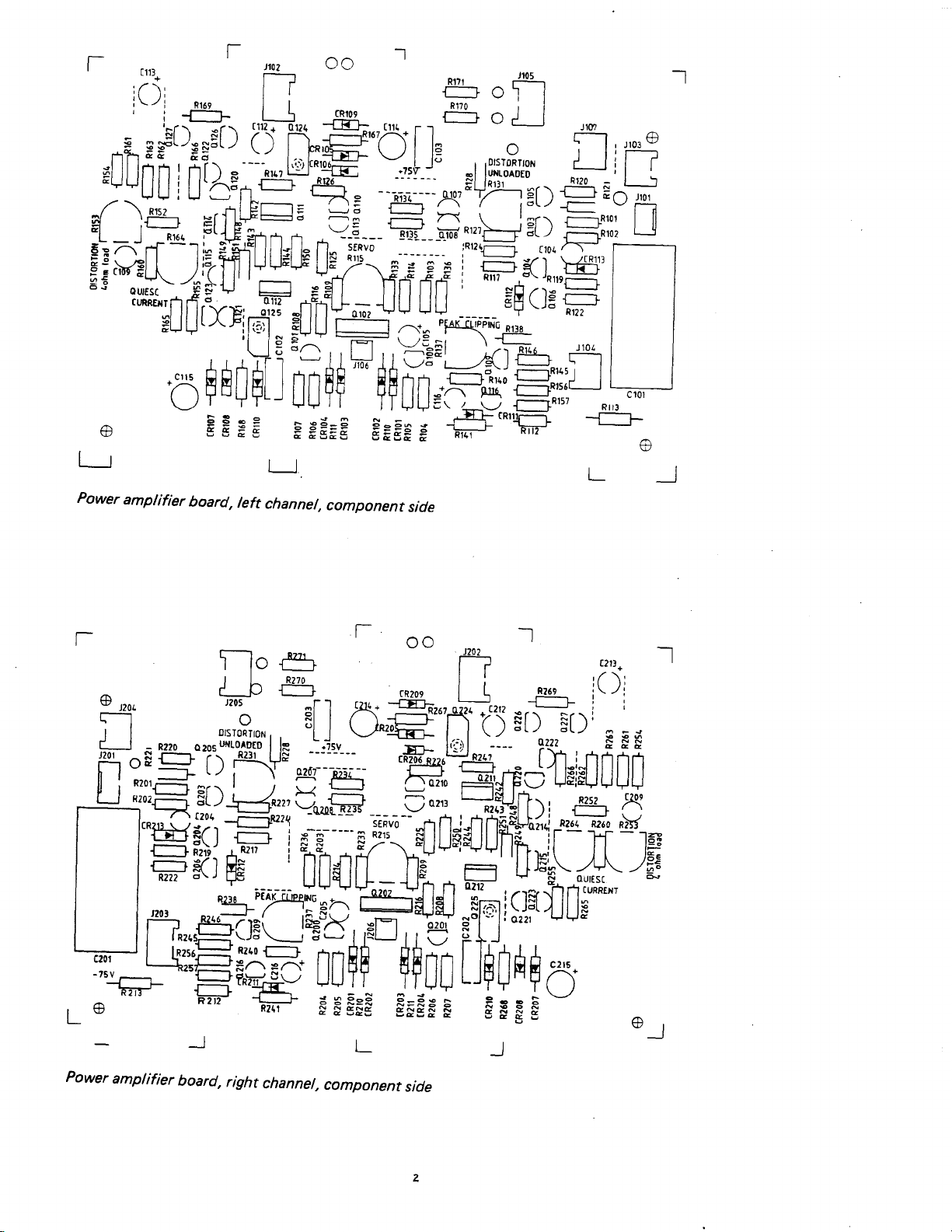
Power
amplifier
cCgE
board,
left
J102
I i
?L & c,,{
\
/'
1.. F
)-#"Ol
l;rc
frj
Efr=
=?:
I :;
1-'1 1.1 r
I n]-*-;;
lt tii tEI
LJEr-rE
=
-!#v;;,+3
0ll2
Adr
nilq_t_"=l|jLlLl
ol25
0l ll
FUL
LJUH-ii"x.i*..
:-''
3
3,*H1;.eFLkE-*,.+i i
lll H$ HEnn-.F*o
JU
?LJ
UU
:ge=g
BEi
channel,
oc
I
L
:
I
I
component
& o#r
&
--
Ir
.'rr-r.
-F'rq--H-'J,:t)
: \
.in-'-
-
-"m'
o
I-J
n,..g,,^' f
Fl ;s,1'*S].- #.iE
l-rr
;pr
F"51,.',H'I
i
;Fc:F
I
I
UUSr
e:cc
g
side
r_..__z
#f
H;;;{_J
]-JRlsi
(R"rr---J
Jrc?
1="C
Enror I li
=:/,
F'"11--s
Rr22
','*@
pi
I
I
L_,6_
Rr3
-G
-fF
-l
T
u
t2o'
il
r, |
_
Rzz'
o:oswroi3lo
?:5.f]
fi
!-r':+
iliEfi
l*Hift+=
t-lo
f
"o'-.
0,,,H,^,,
&
L ,R?70 I I r( )r
L.,
1__l
gll
/\ ffi"'PqT-.;'q nrH
tLJ
q;,hl
_lri,_u___
lJg
i-J'
g-
fr
Q*F
s
i
s..-n
ihh*lrl
l=trj Hf-
l **4;5$$ f-
4$..'=-.#.
F"-r
e
#
-Jlr
F
,
tlft
ss$s
*,
oo
f*P
rRzoe
,&,Llk
#.
on''*B{f'f
e
u*
*ii,'L.ililEiilff,i*11f
trl-'-=
t$,ffi
ftlil
eFsiE
l_
I
c2
f.'l
,R?6e i
str*u,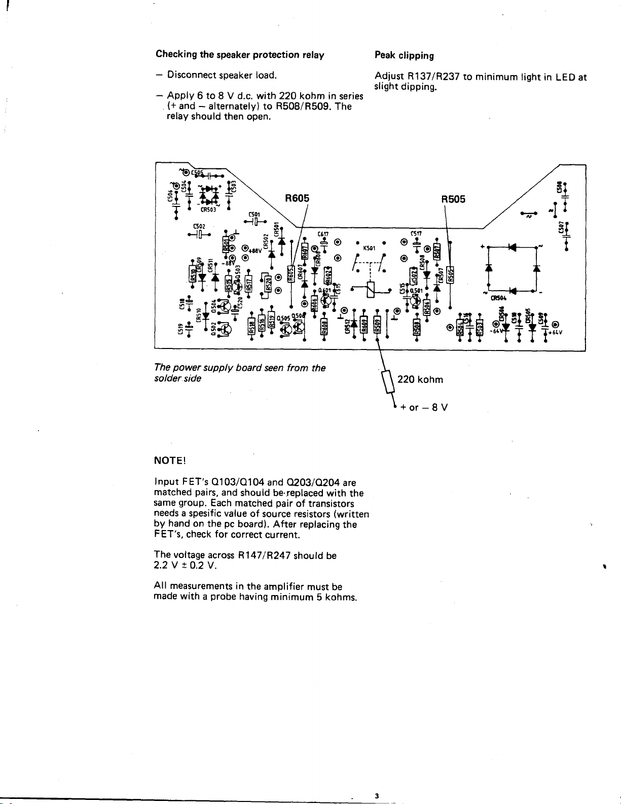
Checking
the
speaker
protection
relay
Peak
clipping
Disconnect
Apply
-
(+
and
relay
should then
speaker
6 to 8 V d.c.
alternatelv) to
-
load.
with 220 kohm in
R508/R509.
open.
Adjust
slight
series
The
bEqF\
fl+ffilf\
T.cRsos-.c5or\l
'
o.r,
-
-10-'
.
1" ffi*"'%1
,ffiffiF!{i
;;'+;gsHBHHt{
R6os
ErY
/g
t617
!l
gc
'fg
r&i
o
+(
o
f,
t4
1o
t'1fi
r
/l
.o
;.
GI
I3
I
?
power
The
solder
supply board
side
seen from
the
R1371R237
dipping.
*.4
'
t,-Et
t
tHt€
_--lq I tu
frItsor' I
-l
=5rl
a I
-
'
9IYE;
-
B'
220
kohm
to
minimum
F
tight
in
LED at
NOTE!
lnput FET's
matched
group.
same
needs
by hand
FET's,
The
voltage
2.2Y t 0.2 V.
All
measurements
made
with
0103/0104
pairs,
Each
a
spesific value
on
the
check
across
probe
a
and
pc
for
correct
matched
in
and O203/O2O4
should be.replaced
board).
R147
having
pair
of
source resistors
After replacing
current.
/R247 should be
the
amplifier
minimum
are
with
of transistors
must be
5
the
(written
the
kohms.
+or-8V
Page 4

or
arl!..
?\
V
---l.:-
*
6rtrn
\ @toeL
H_r__]-r1
/
os
oo,+lQ-6o7dr
; :L'-a
ir.
-1-
l
te
Eg !E
| iJ
-i{54(ftir
g-
-q.
i-
t
'"
r--
ai''"
-----
'iili
F1-4
ir ,.,
'Lii
.f--r :
i-I
POWER
AI.,IP
L.CH
l4
I
tt-
1A
"^'
i
lLTI
sEl rli
r
I
l
Circuit diagram
Page 5

OUTPUT
t________-l
i
POWER L.CH
I
i",
.ln
dr
S.
d t*..
tm
1?C
s0
tr
ll,
ll
r.
t
.Blt.
-a,
Pt
lk
li
tk
tt
ll
6
.td. li lq
rfrril
h
-!t-
t-
.\
FFI:
*I
"I
|
-Tf -ousa"
lii95'tr"
lGr
B
;i
Laf,r
I I
L+.-€H+-
i
POWER
SUPPLY
I
I
I
I
I
**l
I
I
I
I
I
I
I
I
I
I
|
I
:
L-_--_-
fr Oll/a/ar/8
erbt&br.tdfifrth
htur-r t.
ts
.dd.{
aBrd
2rsaol
2X5a5a
2NSr59 2r5452
I
Fr0 R9
d..l6Al
!20
6-?
?-c
1tro
8-9
?t0
9- r0
3!0
I
l0i
!90
6rc
..,-r'ffi!-
h4r.-rrffhEb.'g
ld$
----J
:ola
\rf
\t(
OUTPUT POWTR
L-_----------J
(.lt (.1(
'g:
It.rt 6.il
llr.t ilstr
&{to
a(!..
Itt.r trrBltG!
.rq
ral'
{u^rr
\r!
l&0r
40C0.
^il
gar
R.IH
:
jr \9
?!^n.?
?*r.a?
t
?gral
6xt
l$rt
T*"
r
I
IPART
I
I
INPUT I
I OUTPUI
I
L
I
I
I
I
A
oic
s
LJt
ao.n
&rrt
o G)
'lr
r
\r/
\7
(1
II
ilt'
*'
OH
9
I
--J
""
Notal
lf
vou
with 2N5401 the
changed
The collector
on these
replace
to 82O ohm.
transistors.
.-----_-__J
0120 with 2N5551 end 0121
and
Rl54
base
R155 must be
and
legs are
reversed
Page 6

Dismantling
o Top
cover,
r Top
cover, front
o Rear
r
o
panel (3)
panel (4)
Front
Bottom
Dismantling
rear
cover
the rear
(5)
(1
(2)
)
and top
covers.
w
llit,l
tiii-
lFt
=l
I-I
II
t-l
l-t
=I
=t
l-l
\--\ \-\\
r- \ \-\\
\-l r\\\
r-\ \-\\
l-l l-\\[
l-\ \-\\
l- I l-\\\\
T
\\r
Dismantling the
Adjustments
Test conditions
Approx. 30 minutes
applied. The top and bottom cover should
signal
not be removed,
covered.
Distortion, unloaded
Adjust R131/R231
12 V output, 1 kHz,
should
D.c. offset adjustment
- Solder
-
be
two LED's
opposite
connect
(right)
J206
(collectors
Adjust R115
LED's are switched
front and
otherwise the unit must
less
than
polarity
them
to the contacts
on the
on O'102
(left)
bottom
warming
minimum
to
no load.
and
0.004%.
(light
emitting
together
power
left and
R215
and
off
.
covers.
up time without
distortion, at
The distortion
parallel
in
J106
amplifier
Q202 right).
(right)
be
diodes) with
and
(left)
and
boards
both
until
eG\e
,/
Removethe
on the output terminals.
less
be
Ouiescent current
quiescent
The
load
and
Adjust
output amplifier boards
(left)
and
board.
Distortion,
Apply a signal of 1 kHz and drive the amplifier
on the
12 V
4 ohms.
Adjust
minimum distortion. The
less than 0.005%.
{}--
LED'sand
than t 35 mV.
current
no
signal applied
R164
R605
loaded
output terminals
R131
(left)
(right)
(left)
should
and
and
N
measurethed.c.
The d.c. voltage
be
adjusted
at the input terminals.
(right)
R264
to
35 mV across
on
power
the
when
(right)
R231
distortion should
the
voltage
shou
without
on the
R505
supply
is
load
to
be
ld
to
Page 7

I
I
l
oot
.___rFs....-
i
7/t
tr+fu
Power
Output
-io-
H*"'11
ffi1
ri,1a&;E
Ei-,=s
supply
power
ffi? F!+{
*;,
qdEeq
"f*"r
l6>J
.t!il
<
DR
'...G-
board,
solder side
R 303/(03
OAIE
.
I
l
,
osz62
fl
amplifier board, solder side
t
+ Hl los,
cnnor
*Ht
i $
Ho L.-.-.1
{lg
iffi
6
i
'*so,'
t'
i" lfii
d--
uB'+tH6["'F.
tT.
o-6
6T
.a
EtH
+l
.l
ffi6
"6
R30!O.
U
gcEl
--.-P
DtArFaro|{e
rilrE f
OO
I
I g-
r
+
orgot
nrn
tF
/€q ?
t.=
rdrRcE
I
loltE
RIr/&r
-L__-ts
crl"tl
a
-{
Rgldt
cluaol
crt
*|lq
ta
|
lgte
f4
*rRcE
o
o
o
d=
5
.B-
*oe
t
5
LED board,
.l....
l
I
l-
I
Jo
loooo
lo
lnput board, solder
solder
ooo ooo
0q
o
side
H
H
o o
side
o
o
.$g
*ot*
o
6
+o
o
G
Page 8

Tandberg
Power
Amplifier
TPA
3006 A
,l
Technical Data
Power
requirements:
Powcr
conatmption:
Dimcnsions:
Technicaf
Continuour
ohms, 20
{8
Frequency
Sansitivity:
A-w€ightod
{Ref.
Data according to
Averaga
20.000
-
Rcapon$:
S ignal-to-[{oi3o Retio :
1 W/8 ohms}
Power
Hz, THD <
Output:
l
15/230 Vr
50-770W
Width: 17 1/8"
Depth: 1 3 %"
Heigth: 3 %"
Weight: 25 lbs
10%.50/60
IHF-A-2O2,1978
0.05%)
2xl50W
20.0@ Hz,
20 -
mV
8O
dB
94
{43.5
(35.0
(
8.3
(11.3
+
97- 9.1
Hz
cm)
cm}
cm)
kg)
Secondary
Output
Widcband
SMPTE
I H F
Trsnrient
Reactiye
Rcective
Sepuation:
Diffor€nca
69
Other
Frequenry
Output lmpadanca
Slew
A-w.ighted
(Ref.
Rile
Specifications
without
Disclosures
lmpedancr.(20
Drmping Fector:
I ntermoduletion
I ntermodulation
Ove?load
Load Frctor:
Load Rsting:
Frcguency
of
Technical
Rcgonts:
(20
rato:
ign!l-toJVoir.
S
150
W/8
ohmsl
time:
are
notice.
Hzl:
2O.Od)
-
Oirtortion
Oi3tortion:
Rccovory
Recpon$:
Time:
0.04
200
:
0.05%
0.05%
lmmeasurable
1.7
2.3 dB
>75d8
< 0.1
Data
0.15
+o/-3dB
H:):
2O.OOO
-
Ratio
subject to change for funher
:
0.04 ohms
250 V/sS
117d8
0.9
ss
ohms
dB
Hz
1.5 MHz
-
improvement
.,1
Tandberg
Fetveien
A/S
Box 53
@
'i
o
(\
sl
T
r
z
!?
@
g
tt
<f
o
F
Q
3
q
o
3
z
o
€
N-2007
Kjeller,
Norway
N
F
(D
 Loading...