

T
Enhancement Mode
MOSFET (N-Channel)
Enhancement Mode MOSFET (N-Channel)
Features
• High density cell design for low R
• Voltage controlled small signal switch
• Rugged and reliable
• High saturation current capability
• RoHS Compliance
Mechanical Data
Case:
Terminals:
Weight:
Maximum Ratings (T
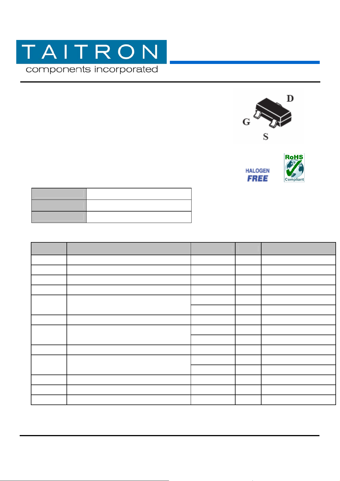
SOT-23, Plastic Package
Solderable per MIL-STD-202G, Method 208
0.008 gram
=25ºC unless noted otherwise)
Ambient
DS(ON)
2N7002
SOT-23
Symbol Description 2N7002 Unit Conditions
VDSS
VDGR
VGSS
VGSM
ID
IDM
PD
RthJA
PD
RthJA
TJ
TSTG
Drain-Source Voltage 60 V
Drain-Gate Voltage (RGS≤1MΩ) 60 V
Gate-Source Voltage Continuous ±20 V
Gate-Source Voltage Non-repetitive (tp≤50µS) ±40 V
Drain Current Continuous (Note 1)
Drain Current Pulsed (Note 2) 800 mA
Total Device Dissipation FR-5 Board (Note 3)
Max. Thermal Resistance, Junction to Ambient 556 ° C/W
Total Device Dissipation Alumina Substrate (Note 4)
Max. Thermal Resistance, Junction to Ambient 417 ° C/W
Junction Temperature
Storage Temperature Range
115 mA TC=25 ˚C
75 mA T
225 mW TA=25 ˚C
1.8 mW/° C Derate above 25 ˚C
300 mW TA=25 ˚C
2.4 mW/° C Derate above 25 ˚C
-55 to +150 ° C
-55 to +150 ° C
C=100 ˚C
Note: 1. The Power Dissipation of thepackage may result in a lower continuous drain current.
TAITRON COMPONEN
Tel: (800)-TAITRON (800)-824-8766 (661)-257-6060
Fax: (800)-TAITFAX (800)-824-8329 (661)-257-6415
S INCORPORATED www.taitroncomponents.com
Rev. B/AH
Page 1 of 6
)
Enhancement Mode MOSFET (N-Channel
2N7002
2. PulseTest: Pulse Width ≤ 300μs, Duty Cycle ≤ 2.0%.
3. FR-5=1.0 x 0.75 x 0.062 in.
4. Alumina=0.4 x 0.3 x 0.025 in 99.5% alumina.
Electrical Characteristics
(T
=25ºC unless noted otherwise)
Ambient
Off Characteristics
Symbol Description Min. Typ. Max. Unit Conditions
V(BR)DSS
IDSS
IGSSF
IGSSR
Drain-Source Breakdown Voltage
Zero Gate Voltage Drain Current
Gate-Body Leakage, Forward - - 0.1 V
Gate-Body Leakage, Reverse - - -0.1
60 - - V V
- - 1 VDS=60V, VGS=0V
- - 500 V
μA
GS=0V, ID=10µA
DS=60V, VGS=0V, TJ=125 ˚C
DS=0V, VGS=20V
DS=0V, VGS=-20V
V
On Characteristics (Note 5)
Symbol Description Min. Typ. Max. Unit Conditions
VGS(th)
Gate Threshold Voltage 1.0 1.6 2.0 V VDS=VGS, ID=250μA
- 1.4 7.5 VGS=10V, ID=500mA
RDS(ON)
VDS(ON)
ID(ON)
gFS
Drain-Source ON Resistance
Drain-Source ON Voltage
On State Drain Current 500 2700 - mA
Forward Transconductance
www.taitroncomponents.com
- 1.7 13.5 VGS=10V, ID=500mA, TJ=125 ˚C
- 1.8 7.5 VGS=5V, ID=50mA
- 2.4 13.5
- 0.6 3.75 VGS=10V, ID=500mA
- 0.09 0.375
80 320 - mS V
Ω
V
V
GS=5V, ID=50mA, TJ=125 ˚C
V
GS=5V, ID=50mA
V
GS=10V,
DS≥2VDS(ON)
V
DS≥2VDS(ON), ID=200mA
Rev. B/AH
Page 2 of 6
)
Enhancement Mode MOSFET (N-Channel
2N7002
Dynamic Characteristics (T
Symbol Description Min. Typ. Max. Unit Conditions
Ciss
Crss
Coss
Input Capacitance - 17 50
Reverse Transfer Capacitance - 2.5 5.0
Output Capacitance - 10 25
=25ºC unless noted otherwise)
Ambient
pF
DS=25V, VGS=0V,
V
f=1MHz
Switching Characteristics
Symbol Description Min. Typ. Max. Unit Conditions
ton
toff
Turn-On Delay Time - 7 20
Turn-Off Delay Time - 11 40
(T
=25ºC unless noted oth er wise )
Ambient
nS
V
DD=25V, RL=50Ω
D=500mA, VGS=10V,
I
R
Drain-Source Diode Ratings and Maximum Ratings
G=25Ω
Symbol Description Min. Typ. Max. Unit Conditions
ID
IDM
VSD
Continuous Drain-Source Diode Forward
Current
Pulsed Drain-Source Diode Forward Current - - 800 mA
Source-Drain Forward Voltage - 0.88 1.5 V VGS=0V, ID=115mA
Note: 5. Pulse Test: Pulse Width≤300μs, Duty Cycle≤2%
www.taitroncomponents.com
- - 115 mA
Rev. B/AH
Page 3 of 6

)
(
)
Enhancement Mode MOSFET (N-Channel
2N7002
Typical Characteristics Curves
Drain Current ID (A)
Fig.3- Temperature vs. Static Drain-Source On-
RDS(ON) (Ω)
Normalized
Fig.1- Ohmic Region
Drain-Source Voltage
Resistance
VDS (V)
Fig.2- Transfer Characteristics
ID (A)
Drain Current
Fig.4- Temperature vs. Gate Threshold Voltage
GS(th) (V)
(Normalized)
Gate-Source Voltage
VGS (V)
Static Drain-Source On-Resistance
Junction Temperature T
J (° C)
Gate-Source Thresh ol d V o lta g e V
Junction Temperature T
J (° C)
Rev. B/AH
www.taitroncomponents.com
Page 4 of 6

)
Enhancement Mode MOSFET (N-Channel
2N7002
Equivalent Circuit
Marking Information:
X: Date Code
Rev. B/AH
www.taitroncomponents.com
Page 5 of 6

)
Enhancement Mode MOSFET (N-Channel
2N7002
Dimensions in mm
How to contact us:
SOT-23
US HEADQUARTERS
28040 WEST HARRISON PARKWAY, VALENCIA, CA 91355-4162
Tel: (800) TAITRON (800) 824-8766 (661) 257-6060
Fax: (800) TAITFAX (800) 824-8329 (661) 257-6415
Email: taitron@taitroncomponents.com
Http://www.taitroncomponents.com
TAITRON COMPONENTS MEXICO, S.A .DE C.V.
BOULEVARD CENTRAL 5000 INTERIOR 5 PARQUE INDUSTRIAL ATITALAQUIA, HIDALGO C.P.
42970 MEXICO
Tel: +52-55-5560-1519
Fax: +52-55-5560-2190
TAITRON COMPONENTS INCORPORATED REPRESENTAÇÕES DO BRASIL LTDA
RUA DOMINGOS DE MORAIS, 2777, 2.ANDAR, SALA 24 SAÚDE - SÃO PAULO-SP 04035-001 BRAZIL
Tel: +55-11-5574-7949
Fax: +55-11-5572-0052
TAITRON COMPONENTS INCORPORATED, SHANGHAI REPRESENTATIVE OFFICE
METROBANK PLAZA, 1160 WEST YAN’ AN ROAD, SUITE 1503, SHANGHAI, 200052, CHINA
Tel: +86-21-5424-9942
Fax: +86-21-5424-9931
Rev. B/AH
www.taitroncomponents.com
Page 6 of 6

 Loading...