

Page 1

X11DPH-I
X11DPH-T
X11DPH-TQ
USER’S MANUAL
Revision 1.2b
Page 2

The information in this user’s manual has been carefully reviewed and is believed to be accurate. The vendor assumes
no responsibility for any inaccuracies that may be contained in this document, and makes no commitment to update
or to keep current the information in this manual, or to notify any person or organization of the updates. Please Note:
For the most up-to-date version of this manual, please see our website at
www.supermicro.com.
Super Micro Computer, Inc. ("Supermicro") reserves the right to make changes to the product described in this manual
at any time and without notice. This product, including software and documentation, is the property of Supermicro and/
or its licensors, and is supplied only under a license. Any use or reproduction of this product is not allowed, except
as expressly permitted by the terms of said license.
IN NO EVENT WILL SUPER MICRO COMPUTER, INC. BE LIABLE FOR DIRECT, INDIRECT, SPECIAL,
INCIDENTAL, SPECULATIVE OR CONSEQUENTIAL DAMAGES ARISING FROM THE USE OR INABILITY TO
USE THIS PRODUCT OR DOCUMENTATION, EVEN IF ADVISED OF THE POSSIBILITY OF SUCH DAMAGES.
IN PARTICULAR, SUPER MICRO COMPUTER, INC. SHALL NOT HAVE LIABILITY FOR ANY HARDWARE,
SOFTWARE, OR DATA STORED OR USED WITH THE PRODUCT, INCLUDING THE COSTS OF REPAIRING,
REPLACING, INTEGRATING, INSTALLING OR RECOVERING SUCH HARDWARE, SOFTWARE, OR DATA.
Any disputes arising between manufacturer and customer shall be governed by the laws of Santa Clara County in the
State of California, USA. The State of California, County of Santa Clara shall be the exclusive venue for the resolution
of any such disputes. Supermicro's total liability for all claims will not exceed the price paid for the hardware product.
FCC Statement: This equipment has been tested and found to comply with the limits for a Class A digital device
pursuant to Part 15 of the FCC Rules. These limits are designed to provide reasonable protection against harmful
interference when the equipment is operated in a commercial environment. This equipment generates, uses, and can
radiate radio frequency energy and, if not installed and used in accordance with the manufacturer’s instruction manual,
may cause harmful interference with radio communications. Operation of this equipment in a residential area is likely
to cause harmful interference, in which case you will be required to correct the interference at your own expense.
California Best Management Practices Regulations for Perchlorate Materials: This Perchlorate warning applies only
to products containing CR (Manganese Dioxide) Lithium coin cells. “Perchlorate Material-special handling may apply.
See
www.dtsc.ca.gov/hazardouswaste/perchlorate”.
WARNING: This product can expose you to chemicals including
lead, known to the State of California to cause cancer and birth
!
defects or other reproductive harm. For more information, go
to www.P65Warnings.ca.gov
.
The products sold by Supermicro are not intended for and will not be used in life support systems, medical equipment,
nuclear facilities or systems, aircraft, aircraft devices, aircraft/emergency communication devices or other critical
systems whose failure to perform be reasonably expected to result in signifi cant injury or loss of life or catastrophic
property damage. Accordingly, Supermicro disclaims any and all liability, and should buyer use or sell such products
for use in such ultra-hazardous applications, it does so entirely at its own risk. Furthermore, buyer agrees to fully
indemnify, defend and hold Supermicro harmless for and against any and all claims, demands, actions, litigation, and
proceedings of any kind arising out of or related to such ultra-hazardous use or sale.
Manual Revision 1.2b
Release Date: September 10, 2019
Unless you request and receive written permission from Super Micro Computer, Inc., you may not copy any part of this
document. Information in this document is subject to change without notice. Other products and companies referred
to herein are trademarks or registered trademarks of their respective companies or mark holders.
Copyright © 2019 by Super Micro Computer, Inc.
All rights reserved.
Printed in the United States of America
Page 3

Preface
Preface
About This Manual
This manual is written for system integrators, IT technicians, and knowledgeable end users.
It provides information for the installation and use of the X11DPH-i/T(q) motherboard.
About This Motherboard
The X11DPH-i/X11DPH-T/X11DPH-Tq motherboard supports dual Intel® Xeon Scalable-SP
and 2nd Generation Intel® Xeon Scalable-SP (Socket P) processors with the TDP (Thermal
Design Power) of up to 205W and three UltaPath Interconnect (UPI) links of up to 10.4 GT/s.
With the Intel C621/C622/C627* chipset built-in, this motherboard supports seven PCI-E
3.0 x16/x8 slots, two PCI-E 3.0 x4 M.2 slots, ten SATA3 ports, seven USB 3.0 connections,
and up to 4TB of 3DS LRDIMM/LRDIMM/3DS RDIMM/RDIMM/NV-DIMM DDR4 ECC
2933**/2666/2400/2133 MHz memory in 16 memory slots. (See Notes 1, 2 below.) It also
supports up to 5TB memory with DCPMM*** modules. (See Note 3 below.) This motherboard
is optimized for PCI-E expansion with fl exible IO support, and is ideal for high-performance,
general-purpose server platforms. Please note that this motherboard is intended to be installed
and serviced by professional technicians only. For processor/memory updates, please refer
to our website at http://www.supermicro.com/products/.
Notes:
1. Intel C621 is used for X11DPH-i, C622 for X11DPH-T, and C627 for X11DPT-Tq.
2. 2933 MHz memory is supported by the 2nd Generation Intel Xeon Scalable-SP
(82xx/62xx series) processors only.
3. DCPMM memory is supported by the 2nd Generation Intel Xeon Scalable-SP
(82xx/62xx/52xx/42xx series) processors only.
4. UPI/memory speeds are dependent on the processors installed in your system.
Manual organization
Chapter 1 describes the features, specifi cations, and performance of the motherboard. It
provides detailed information on the Intel processors and chipset.
Chapter 2 provides hardware installation instructions. Read this chapter when installing the
processor, memory modules, and other hardware components into the system.
Chapter 3 describes troubleshooting procedures for video, memory, and system setup stored
in the CMOS.
Chapter 4 includes an introduction to the BIOS, and provides detailed information on running
the CMOS setup utility.
3
Page 4

Super X11DPH-i/X11DPH-T/X11DPH-Tq User's Manual
Appendix A provides BIOS Error Beep codes.
Appendix B lists software installation instructions.
Appendix C lists standardized warning statements in various languages.
Appendix D contains UEFI BIOS Recovery instructions.
Appendix E provides information on how to confi gure VROC RAID settings.
Appendix F provides information on how to confi gure secure boot settings.
Appendix G provides information on how to confi gure iSCSI settings.
Appendix H provides information on how to confi gure Network Interface Card (NIC) settings.
4
Page 5

Contacting Supermicro
Headquarters
Address: Super Micro Computer, Inc.
980 Rock Ave.
San Jose, CA 95131 U.S.A.
Tel: +1 (408) 503-8000
Fax: +1 (408) 503-8008
Email: marketing@supermicro.com (General Information)
support@supermicro.com (Technical Support)
Contacting Supermicro
Website:
Europe
Address: Super Micro Computer B.V.
Tel: +31 (0) 73-6400390
Fax: +31 (0) 73-6416525
Email: sales@supermicro.nl (General Information)
Website:
Asia-Pacifi c
Address: Super Micro Computer, Inc.
www.supermicro.com
Het Sterrenbeeld 28, 5215 ML
's-Hertogenbosch, The Netherlands
support@supermicro.nl (Technical Support)
rma@supermicro.nl (Customer Support)
www.supermicro.nl
3F, No. 150, Jian 1st Rd.
Zhonghe Dist., New Taipei City 235
Taiwan (R.O.C)
Tel: +886-(2) 8226-3990
Fax: +886-(2) 8226-3992
Email: support@supermicro.com.tw
Website:
www.supermicro.com.tw
5
Page 6

Super X11DPH-i/X11DPH-T/X11DPH-Tq User's Manual
Table of Contents
Chapter 1 Introduction
1.1 Checklist ...............................................................................................................................8
1.2 Processor and Chipset Overview .......................................................................................18
1.3 Special Features ................................................................................................................19
1.4 System Health Monitoring ..................................................................................................19
1.5 ACPI Features ....................................................................................................................20
1.6 Power Supply .....................................................................................................................20
1.7 Advanced Power Management ..........................................................................................20
1.8 Intel® QuickAssist Technology (For the X11DPH-Tq only) ................................................21
1.9 Intel® Optane DC Persistent Memory Overview ...............................................................21
Chapter 2 Installation
2.1 Static-Sensitive Devices .....................................................................................................22
2.2 Motherboard Installation .....................................................................................................23
2.3 Processor and Heatsink Installation ...................................................................................25
2.4 Memory Support and Installation .......................................................................................33
Memory Support ................................................................................................................33
General Memory Population Requirements ......................................................................33
DDR4 Memory Support for Intel Xeon Scalable-SP Processors ......................................34
DDR4 Memory Support for 2nd Gen Intel Xeon Scalable-SP Processors .......................34
DIMM Population Guidelines for Optimal Performance ....................................................35
DIMM Population Table .....................................................................................................36
DIMM Installation ..............................................................................................................38
DIMM Module Removal .....................................................................................................38
2.5 Rear I/O Ports ....................................................................................................................39
2.6 Front Control Panel ............................................................................................................44
2.7 Connectors .........................................................................................................................49
2.8 Jumper Settings .................................................................................................................59
2.9 LED Indicators ....................................................................................................................62
Chapter 3 Troubleshooting
3.1 Troubleshooting Procedures ..............................................................................................64
3.2 Technical Support Procedures ...........................................................................................68
3.3 Frequently Asked Questions ..............................................................................................69
3.4 Battery Removal and Installation .......................................................................................70
6
Page 7

Table of Contents
3.5 Returning Merchandise for Service ....................................................................................71
Chapter 4 UEFI BIOS
4.1 Introduction .........................................................................................................................72
4.2 Main Setup .........................................................................................................................73
4.3 Advanced Setup Confi gurations .........................................................................................75
4.4 Event Logs .......................................................................................................................122
4.5 IPMI ..................................................................................................................................124
4.6 Security Settings ..............................................................................................................127
4.7 Boot Settings ....................................................................................................................131
4.8 Save & Exit .......................................................................................................................134
Appendix A BIOS Codes
A.1 BIOS Error POST (Beep) Codes .....................................................................................136
A.2 Additional BIOS POST Codes ..........................................................................................137
Appendix B Software
B.1 Microsoft Windows OS Installation ...................................................................................138
B.2 Driver Installation ..............................................................................................................140
B.3 SuperDoctor
B.4 IPMI ..................................................................................................................................142
®
5 .................................................................................................................141
Appendix C Standardized Warning Statements
Appendix DUEFI BIOS Recovery
Appendix E Confi guring VROC RAID Settings
E.1 All Intel® VMD Controllers Features ................................................................................151
E.2 Confi guring RAID Settings ...............................................................................................158
E.3 Use of Journaling Drive ....................................................................................................171
Appendix F Secure Boot Settings
F.1 Boot mode select Feature ................................................................................................175
F.2 Secure Boot/ Secure Boot Mode/ CSM Support Features ..............................................176
F.3 Secure Boot Settings .......................................................................................................177
F.4 Key Management Settings ...............................................................................................180
Appendix G Confi guring iSCSI Settings
G.1 PCIe/PCI/PnP Features ....................................................................................................197
G.2 Confi guring iSCSI Settings ...............................................................................................200
Appendix H Confi guring Network Interface Card (NIC) Settings
H.1 Network Interface Card (NIC) Settings ............................................................................220
7
Page 8

Super X11DPH-i/X11DPH-T/X11DPH-Tq User's Manual
Chapter 1
Introduction
Congratulations on purchasing your computer motherboard from an industry leader.
Supermicro motherboards are designed to provide you with the highest standards in quality
and performance.
In addition to the motherboard, several important parts that are included with your shipment
are listed below. If anything listed is damaged or missing, please contact your retailer.
1.1 Checklist
Main Parts List
Description Part Number Quantity
Supermicro motherboard (X11DPH-i/X11DPH-T/X11DPH-Tq) MNL-1912 1
SATA cables CBL-0044L (x2) 2
I/O Shield MCP-260-00042-ON 1
Important Links
For your system to work properly, please follow the links below to download all necessary
drivers/utilities and the user’s manual for your system.
• Supermicro product manuals: http://www.supermicro.com/support/manuals/
• Product drivers and utilities: http://www.supermicro.com/wftp
• Product safety info: http://www.supermicro.com/about/policies/safety_information.cfm
• If you have any questions, please contact our support team at: support@supermicro.com
his manual may be periodically updated without notice. Please check the Supermicro website
T
for possible updates to the manual revision level.
8
Page 9
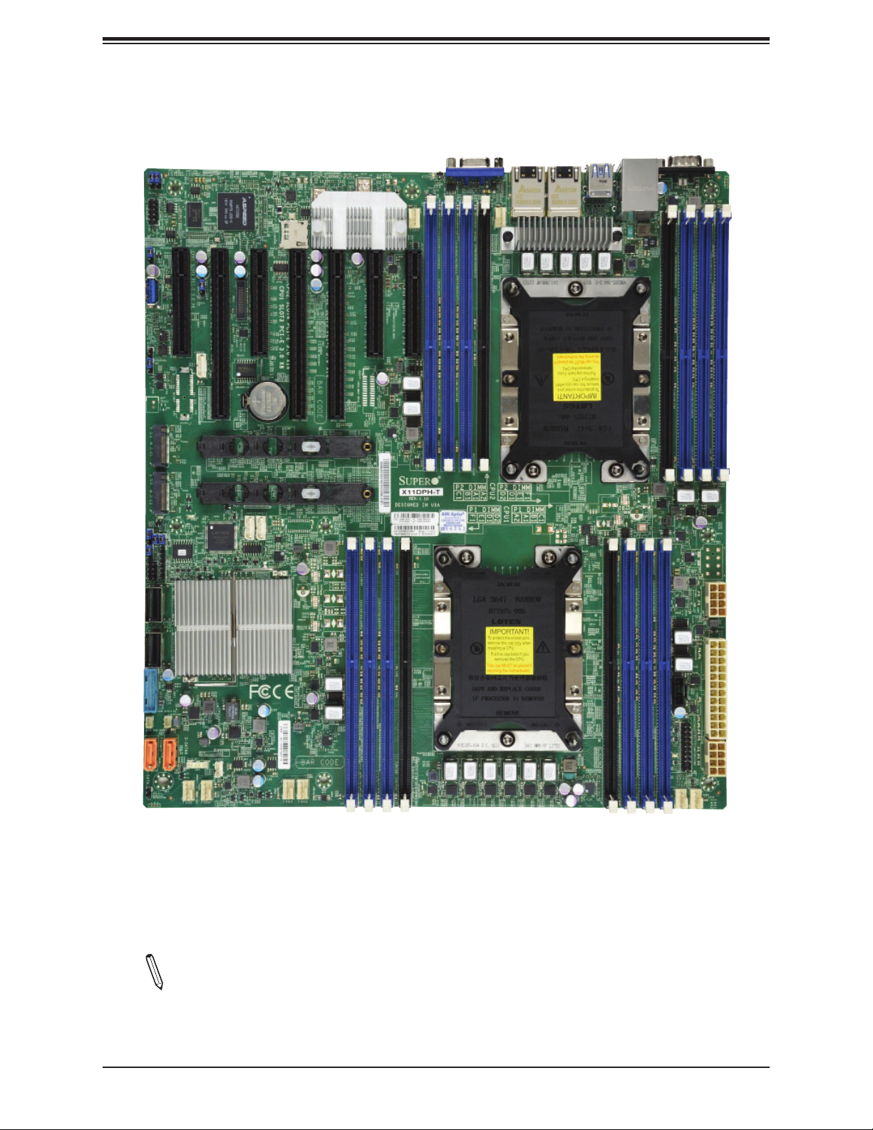
X11DPH-i/T(q) Motherboard Image
Chapter 1: Introduction
Note: All graphics shown in this manual were based upon the latest PCB revision
available at the time of publication of the manual. The motherboard you received may
or may not look exactly the same as the graphics shown in this manual.
9
Page 10
Super X11DPH-i/X11DPH-T/X11DPH-Tq User's Manual
USB 2/3(3.0)
LE1
JUIDB1
JTPM1
JPME2
CPU1 SLOT1 PCI-E 3.0 x8
USB 6 (3.0)
BMC
LEDM1
ASPEED
AST2500
CPU2 SLOT2 PCI-E 3.0 x16
CPU1 SLOT3 PCI-E 3.0 x8
JNCSI
JSDCARD1
CPU2 SLOT5 PCI-E 3.0 x16
CPU2 SLOT4 PCI-E 3.0 x16
LAN
CTRL
CPU1 SLOT6 PCI-E 3.0 x8
FAN6
CPU1 SLOT7 PCI-E 3.0 x8
VGA
FAN5
LAN2
LAN1
IPMI_LAN
USB 0/1(3.0)
COM1
JD1
JP4
M.2-C1
M.2-C2
LE4
JWD1
T-SGPIO1
JSD1
SATA2
JL1
BIOS
I- SATA 0~3
I- SATA 4~7
USB 4/5(3.0)
JSD2
S-SATA0
S-SATA1
SATA1
FANB
LE3
JRK1
JIPMB1
FANA
Intel
PCH
JSTBY1
CPU1-HSSI GPIO
P1-DIMMD2
JHSSI
P2-DIMMA2
P2-DIMMA1
P2-DIMMB1
P2-DIMMC1
MAC CODE
BAR CODE
BIOS LICENSE
X11DPH-i
REV: 1.10
Battery
+
BT1
MH4
MH11
P1-DIMMD1
P1-DIMME1
JBT1
P1-DIMMF1
CPU2
P1-DIMMA1
P1-DIMMA2
P2-DIMMD2
P1-DIMMC1
P1-DIMMB1
P2-DIMMD1
P2-DIMME1
JPWR4
JPWR2
P2-DIMMF1
CPU1
JPWR3
JPI2C1
JF1
IPMI CODE
FAN4 FAN 3
LE2
JPWR1
FAN2
FAN1
Note: All graphics shown in this manual were based upon the latest PCB revision
available at the time of publication of the manual. The motherboard you received may
or may not look exactly the same as the graphics shown in this manual.
10
Page 11
Chapter 1: Introduction
JTPM1
JPME2
USB6 (3.0)
JD1
JIPMB1
JP4
BT1
M.2-C1
M.2-C2
LE3
LE4
JWD1
JBT1
T-SGPIO1
I-SATA 0~3
I-SATA 4~7
USB4/5 (3.0)
JSD2
JSD1
S-SATA1
S-SATA0
JL1
LEDM1
SLOT1
JTPM1
JPME2
USB 6 (3.0)
JD1
JP4
M.2-C1
M.2-C2
LE4
JWD1
T-SGPIO1
USB 4/5(3.0)
JSD1
S-SATA1
SATA2
JL1
FANB
JRK1
SLOT3
JNCSI
SLOT2
BMC
LEDM1
ASPEED
AST2500
CPU2 SLOT2 PCI-E 3.0 x16
CPU1 SLOT1 PCI-E 3.0 x8
JIPMB1
LE3
BIOS
I-S ATA 0~3
JSD2
S-SATA0
FANB
JRK1
FANA
Intel
PCH
JSTBY1
I-S ATA 4~7
SATA1
JSTBY1
FANA
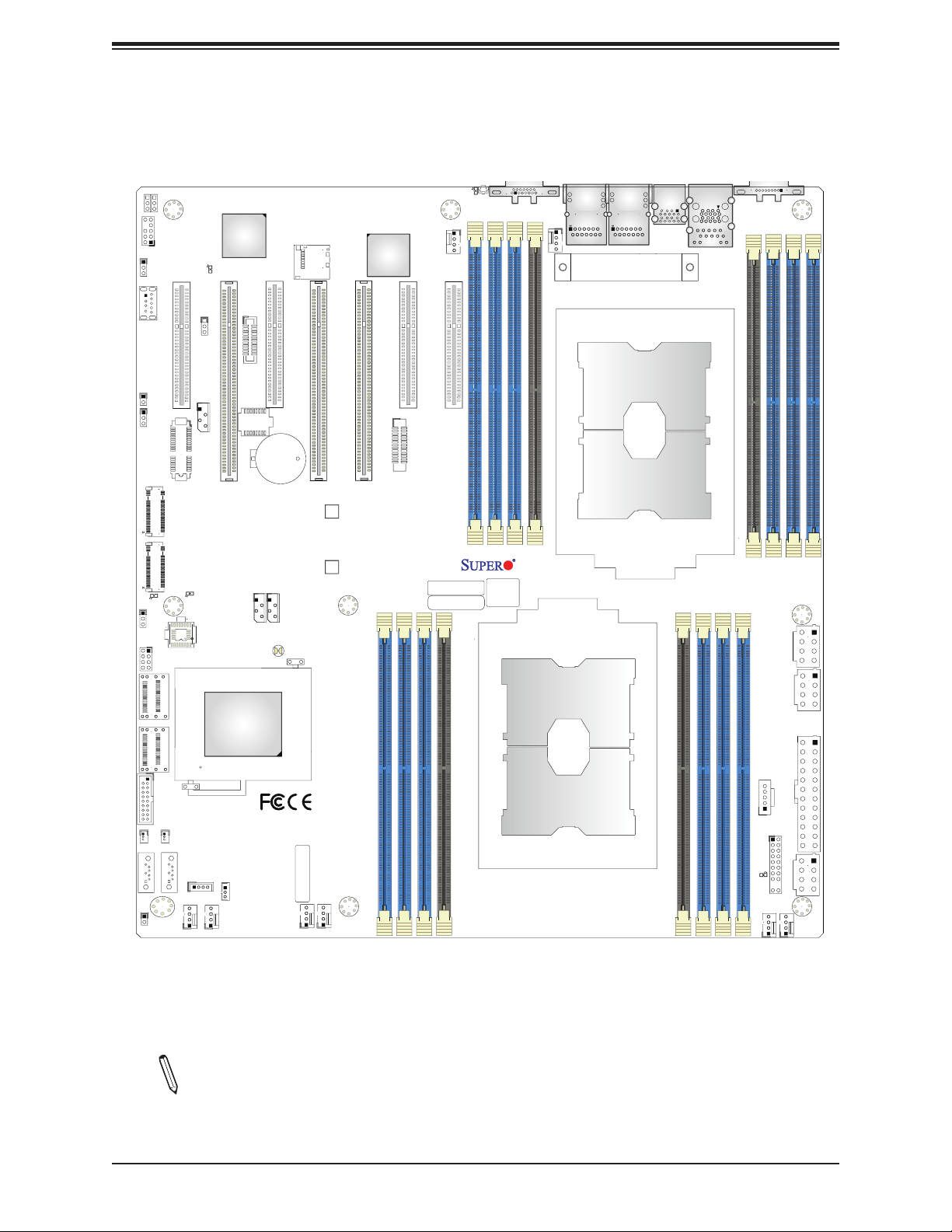
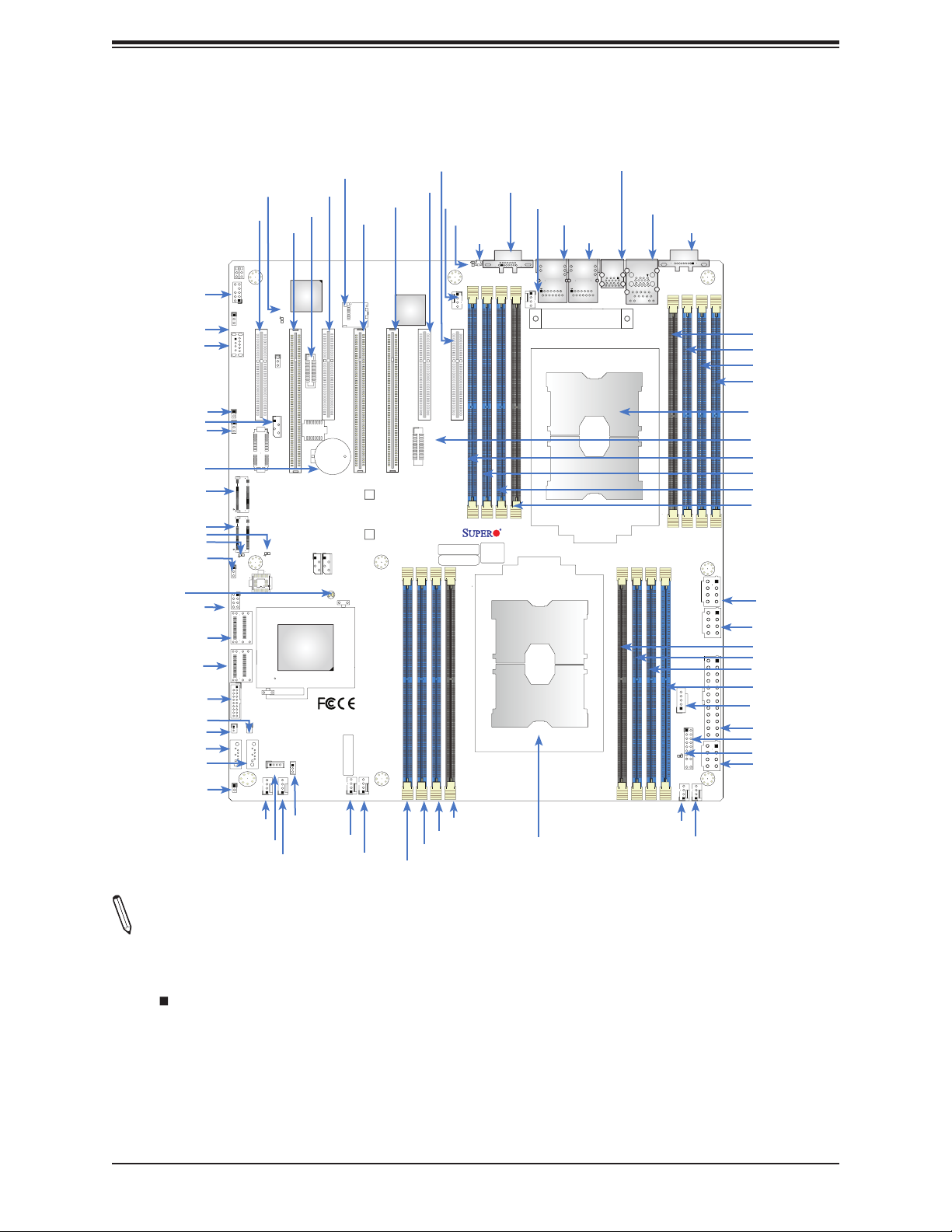
X11DPH-i/T(q) Motherboard Layout
(not drawn to scale)
JSDCARD1
SLOT4
JSDCARD1
CPU1 SLOT3 PCI-E 3.0 x8
CPU2 SLOT4 PCI-E 3.0 x16
JNCSI
Battery
+
BT1
JBT1
IPMI CODE
FAN4 FAN3
FAN4
FAN3
SLOT5
MH4
MH11
SLOT7
SLOT6
LAN
CTRL
CPU2 SLOT5 PCI-E 3.0 x16
CPU1 SLOT6 PCI-E 3.0 x8
CPU1-HSSI GPIO
JHSSI
P1-DIMMD2
P1-DIMMD1
P1-DIMME1
P1-DIMMF1
P1-DIMMD1
P1-DIMME1
P1-DIMMF1
FAN6
VGA
LE1
JUIDB1
LE1
JUIDB1
FAN6
CPU1 SLOT7 PCI-E 3.0 x8
P2-DIMMA2
P2-DIMMA1
P2-DIMMB1
P2-DIMMC1
MAC CODE
BIOS LICENSE
BAR CODE
P1-DIMMD2
FAN5
VGA
FAN5
X11DPH-i
REV: 1.10
LAN2
LAN2
CPU1
CPU1
USB2/3 (3.0)
LAN1
USB 2/3(3.0)
LAN1
CPU2
IPMI LAN
USB0/1 (3.0)
IPMI_LAN
USB 0/1(3.0)
P2-DIMMD2
P1-DIMMA1
P1-DIMMA2
P1-DIMMC1
P1-DIMMB1
JPI2C1
FAN2
COM1
COM1
P2-DIMMD1
JF1
LE2
FAN2
FAN1
P2-DIMME1
JPWR4
JPWR2
JPWR3
JPWR1
FAN1
P2-DIMMF1
P2-DIMMD2
P2-DIMMD1
P2-DIMME1
P2-DIMMF1
CPU2
JHSSI
P2-DIMMC1
P2-DIMMB1
P2-DIMMA1
P2-DIMMA2
JPWR4
JPWR2
P1-DIMMA2
P1-DIMMA1
P1-DIMMB1
P1-DIMMC1
JPI2C1
JPWR3
JF1
LE2
JPWR1
Notes:
• See Chapter 2 for detailed information on jumpers, I/O ports, and JF1 front panel con-
nections.
• " " indicates the location of Pin 1.
• Jumpers/LED indicators not documented in this user manual are reserved for internal
testing only.
• Use only the correct type of onboard CMOS battery as specifi ed by the manufacturer. Do
not install the onboard battery upside down to avoid possible explosion.
11
Page 12

Super X11DPH-i/X11DPH-T/X11DPH-Tq User's Manual
Quick Reference Table
Jumper Description Default Setting
JBT1 CMOS Clear Open (Normal)
JPME2 ME Manufacturing Mode Pins 1-2 (Normal)
JWD1 Watch Dog Timer Enable Pins 1-2 (Reset)
Connector Description
BT1 Onboard CMOS battery
COM1 COM port on the I/O back panel
FAN1-6, FANA/FANB System/cooling fan headers
IPMI_LAN Dedicated IPMI LAN port
I-SATA0~3, I-SATA4~7 SATA 3.0 Ports supported by the Intel PCH
JD1 Speaker/buzzer header (use in conjunction with an external speaker/buzzer) (optional)
JF1 Front control panel header
JHSSI High-Speed Serial Interface (HSSI) card header
JIPMB1 4-pin External I2C Header (for an IPMI card)
JL1
JNCSI Network Controller Sideband Interface (NCSI) header
JPI2C1 Power I2C System Management Bus (SMBus) header
JPWR1, JPWR2, JPWR4 8-pin power supply connectors
JPWR3 24-pin ATX main power supply connector
JRK1 Intel RAID key for NVMe SSD (Solid State Devices)
JSD1, JSD2 SATA DOM (Device-on-Module) power connectors
JSDCARD1 Micro SD card slot
JSTBY1 Standby power header
JTPM1 Trusted Platform Module (TPM)/Port 80 connector
JUIDB1 Unit Identifi er (UID) switch
LAN1, LAN2 10GbE LAN ports (for the X11DPH-T(q)) and Gigabit LAN ports (for the X11DPH-i)
M.2-C1, M.2-C2 PCI-E M.2 slots (w/VMD support) (See the notes below.)
MH4, MH11 M.2 mounting holes
(CPU1) SLOT1, SLOT3,
SLOT6, SLOT7
(CPU2) SLOT2, SLOT4,
SLOT5
S-SATA0, S-SATA1
Chassis intrusion header (For this feature to work properly, please connect an optional external
speaker to the onboard speaker header at JD1.)
PCI-Express 3.0 x8 Slots supported by CPU1 (See the notes below.)
PCI-Express 3.0 x16 Slot supported by CPU2 (See the notes below.)
Powered SATA 3.0 ports with support of Supermicro SuperDOM (Disk-On-Module)
Note 1: Intel VMD is supported by PCI-E Slot 1 - Slot 7, M.2-C1 ,and M.2-C2 slots. 2:
After you’ve enabled VMD in the BIOS on a PCI-E slot of your choice, this PCI-E slot
will be dedicated for VMD use only, and it will no longer support any PCI-E device.
To re-activate this slot for PCI-E use, please disable VMD in the BIOS. 3: To avoid
interference with other components, please be sure to use an add-on card that is fully
compliant with the PCI Standards on a PCI slot.
12
Page 13

Chapter 1: Introduction
Connector Description
T-SGPIO1 Serial_Link General Purpose I/O (GPI/O) port
USB0/1, USB2/3 Back Panel Universal Serial Bus (USB) 3.0 ports
USB4/5 Internal USB 3.0 header with two USB (USB4/5) connections supported for front access
USB6 Type A USB 3.0 header for front access
VGA VGA port
LED Description Status
LE1 Unit Identifi er (UID) LED Solid Blue: Unit Identifi ed
LE2 Onboard power LED Solid Green: Power On
LEDM1 BMC Heartbeat LED Blinking Green: BMC normal
13
Page 14

Super X11DPH-i/X11DPH-T/X11DPH-Tq User's Manual
Motherboard Features
Motherboard Features
CPU
• Dual Intel Xeon Scalable-SP or 2nd Generation Intel Xeon Scalable-SP (Socket P) processors with support of three
UltraPath Interconnect (UPI) links of up to 10.4 GT/s. (Note: QAT is supported by X11DPH-Tq only.)
Note: Both processors need to be installed for full access to the PCI-E slots, DIMM slots, and onboard controllers.
Refer to the block diagram to determine which slots or devices may be affected.
Memory
• Integrated memory controller supports up to 4TB of 3DS Load Reduced DIMM (3DS LRDIMM), Load Reduced DIMM
(LRDIMM), 3DS Registered DIMM (3DS RDIMM), Registered DIMM (RDIMM), Non-Volatile DIMM (NV-DIMM) DDR4
(288-pin) ECC memory with speeds of 2933*/2666/2400/2133 in 16 slots
Notes: 1. Up to 5TB of memory is supported with DCPMM modules installed. 2. 2933 MHz memory is supported
by 2nd Gen Intel Xeon Scalable-SP (82xx/62xx series) processors only.
DIMM Size
• Up to 256GB at 1.2V
Note 1: Memory speed support depends on the processors used in the system.
Note 2: For the latest CPU/memory updates, please refer to our website at http://www.supermicro.com/products/
motherboard.
Chipset
• Intel C621/C622/C627 Chipset (C621: is for X11DPH-i, C622 for X11DPH-T, and C627: X11DPT-Tq.)
Expansion Slots
• Four (4) PCI-Express 3.0 X8 slots supported by CPU1 (SLOT1, SLOT3, SLOT6, SLOT7 3; No Slot1 for X11DPH-Tq)
• Three (3) PCI-Express 3.0 X16 slots supported by CPU2 (SLOT2, SLOT4, SLOT5)
Baseboard Management Controller (BMC)
• ASPEED AST2500 BMC with IPMI 2.0 support
Graphics
• Graphics controller via ASPEED AST2500 BMC
Network Connection
• Intel C627 supports two 10 Gigabit LAN ports on the X11DPH-Tq
• Intel C622 supports two 10 Gigabit LAN ports on the X11DPH-T
• Intel C621 supports two Gigabit LAN ports (X11DPH-i)
• One (1) Dedicated IPMI LAN located on the rear I/O panel
I/O Devices
• Serial (COM) Port • One (1) serial port on the rear I/O panel
• SATA 3.0
• Eight (8) SATA 3.0 ports (I-SATA0~3, I-SATA4~7)
• Two (2) SATA 3.0 ports with SATA DOM power (S-SATA0, S-SATA1)
• RAID (PCH) • RAID 0, 1, 10
Note: Please refer to the Memory Confi guration User Guide for the X11 UP/DP/MP
Motherboards posted on our website for detailed information on memory support.
14
Page 15

Chapter 1: Introduction
Motherboard Features
Peripheral Devices
• Four (4) USB 3.0 ports on the I/O back panel (USB 0/1, USB2/3)
• One (1) USB 3.0 header with two (2) USB connections for front access (USB4/5)
• One (1) USB 3.0 Type A header (USB6)
BIOS
• 64MB SPI AMI BIOS® SM Flash UEFI BIOS
• ACPI 3.0 or later, USB keyboard, Plug-and-Play (PnP), SPI dual/quad speed support, and SMBIOS 2.7 or later
Power Management
• ACPI power management
• SuperDoctor® 5
• Power button override mechanism
• Power-on mode for AC power recovery
• Intel® Intelligent Power Node Manager 4.0 (available when the Supermicro Power Manager [SPM] is installed and a
special power supply is used
• Management Engine (ME)
System Health Monitoring
• Onboard voltage monitoring for +5V, +/-12V, +3.3V Standby, +5V Standby, HT, memory, PCH temperature, system
temperature, and memory temperature
• 6+1 CPU switch phase voltage regulator for CPU1
• 5+1 CPU switch phase voltage regulator for CPU2
• CPU thermal trip support
• Status monitor for on/off control
• CPU Thermal Design Power (TDP) support of up to 165W
Fan Control
• Fan status monitoring via IPMI
• Eight 4-pin fan headers
• Dual cooling zone
• Multi-speed fan control via onboard BMC
System Management
• Trusted Platform Module (TPM) support
• PECI (Platform Environment Control Interface) 2.0 support
• System resource alert via SuperDoctor® 5
• SuperDoctor® 5, Watch Dog, NMI, RoHS
• Power supply monitoring
• Chassis intrusion header and detection (when an optional external speaker is connected to the onboard speaker header
at JD1)
15
Page 16

Super X11DPH-i/X11DPH-T/X11DPH-Tq User's Manual
Motherboard Features
LED Indicators
• CPU/Overheating
• Power/Suspend-state indicator
• Fan failure
• UID/remote UID.
• HDD activity
• LAN activity.
Dimensions
•
13" (W) x 12" (L) (330.2 mm x 304.8 mm)
Note 1: The CPU maximum thermal design power (TDP) is subject to chassis and
heatsink cooling restrictions. For proper thermal management, please check the chassis and heatsink specifi cations for proper CPU TDP sizing.
Note 2: For IPMI confi guration instructions, please refer to the Embedded IPMI Con-
fi guration User's Guide available at http://www.supermicro.com/support/manuals/.
Note 3: It is strongly recommended that you change BMC log-in information upon initial
system power-on. The manufacturer default username is ADMIN and the password
is ADMIN. For proper BMC confi guration, please refer to http://www.supermicro.com/
products/info/fi les/IPMI/Best_Practices_BMC_Security.pdf
16
Page 17
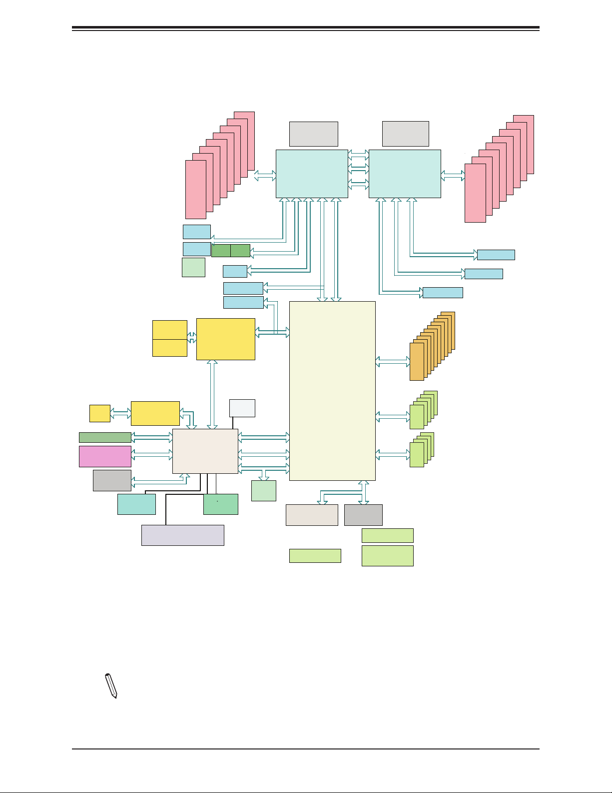
System Block Diagram
Chapter 1: Introduction
RJ45
DDR4
BMC Boot Flash
BIOS
(OPTION)
* TBD
LAN3
RTL8211E-VB-CG
SPI
SPI
VGA CONN
Temp Sensor
EMC1402-1 *2 at diff SMBUS
SLOT 7
(HSSI)
SLOT 6
(HSSI)
10G
1G
10G
1G
#B-0
#A-1
#A-0
DDR4
2133/2666/2933*
PCI-E x8
PCI-E x8
HSSI
GPIO
LAN
Intel X557-AT2
Marvell 88E1512
RGRMII
BMC
AST2500
#F-0
#E-0
#D-1
#D-0
#C-0
PCI-E X8/X8 G3 (Reversal)
M.2
M.2
SLOT 3
PCI-E x8 G3 (Reversal)
PCI-E x8
SLOT 1
PCI-E x8
PCI-E x1
(QAT AOC)
RMII/NCSI
Micro
SDCard
PCI-E x1 G2
USB 2.0
COM1
Connector
#3
PCI-E x4/x4 G3
PCI-E x8 G3(Opt)
4x10G(Opt)
ESPI
ESPI
Header
VCCP0 12v
VR13
6+1 PHASE
up to 255W
VCCP0
SNB CORE
DDR4
#2C #1B/A
#2A/B
KR/KX/SFI
#5
#12 USB2.0
TPM HEADER
Debug Card
FRONT PANEL
X11DPH
10.4/11.2G
P0
P1
PECI: 30
SOCKET ID: 0
DMI3
PCI-E x8 G3 (Opt x16)
DMI3
PCH
(QAT: Optional x16)
VCCP1 12v
VR13
P1
P0
P2P2
#1
5+1 PHASE
VCCP1
SNB CORE
DDR4
SOCKET ID: 1
#2
#3
PCI-E x16 G3 (Reversal)
PCI-E x16 G3
#3
#2
#1
#0
6.0 Gb/S
USB 2.0
USB 3.0
PECI: 31
DMI2
PCI-E x16 G3 (Reversal)
#6
#5
#4
SATA
USB
USB
UPI
UPI
UPI
UPI
*Note: 2933 memory is supported
by 2nd Gen Intel Xeon Scalable-SP
SPI
(82xx/62xx series) processors only.
BIOS
SYSTEM POWER
FAN SPEED
CTRL
PCI-E x16
SLOT 2
#9
#8
#7
6 CH6 CH
iPass 4x2
SuperDOM x2
Rear x4
Header x2
Type A x1
#H-0
#G-1
#G-0
DDR4
2133/2666/2933*
PCI-E x16
SLOT 4
PCI-E x16
SLOT 5
#J-0
#K-0
#K-1
#L-0
#M-0
Note: This is a general block diagram and may not exactly represent the features on
your motherboard. See the previous pages for the actual specifi cations of your moth-
erboard.
17
Page 18

Super X11DPH-i/X11DPH-T/X11DPH-Tq User's Manual
1.2 Processor and Chipset Overview
Built upon the functionality and capability of Intel Xeon Scalable-SP and 2nd Generation
Intel Xeon Scalable-SP processors (Socket P) with support of the Intel C621/C622/C627
chipset (Note 1), the X11DPH-i/X11DPH-T/X11DPH-Tq motherboard provides superb system
performance, effi cient power management, and a rich feature set based on cutting-edge
technologies to address the needs of next-generation computer users. It offers innovative
solutions with unprecedented system reliability and scalability to meet the demands of High
Performance Computing (HPC) platforms.
Features Supported by Intel Xeon Scalable-SP Processors
Intel Xeon Scalable-SP processors support the following features:
• Intel AVX-512 instruction support to handle complex workloads
• 1.5x memory bandwidth increased to 6 channels
• Hot plug and enclosure management with Intel Volume Management Device (Intel VMD)
• Rich set of available IOs with increased PCI-E lanes (48 lanes)
• Integrated Intel Ethernet Connection X722 with iWARP RDMA
New features supported by 2nd Generation Intel Xeon Scalable-SP Processors
2nd Generation Intel Xeon Scalable-SP processors support the following features:
• Higher performance for a wider range of workloads with per-core performance in-
crease
• Support of Optane DC Persistent Memory (DCPMM) with affordable, persistent, and
large capacity
• Up to 2993 MHz memory supported (Refer to Section 1.9 for details.)
• Vector Neural Network Instruction (VNNI) support for Accelerate Deep Learning & Arti-
fi cial Intelligence (AI) workloads
• Speed Select Technology provides multiple CPU profi les that can be set in the BIOS.
(This feature is available on select CPU SKUs).
• Seamless hardware security mitigations & performance/frequency fl exibility
Notes: 1. Intel C621 is used for X11DPH-i, C622 for X11DPH-T, and C627 for
X11DPT-Tq. 2. DCPMM memory is supported by 2nd Gen Intel Xeon Scalable-SP
(82xx/62xx/52xx/42xx series) processors. 3. 2933 MHz memory is supported by 2nd
Gen Intel Xeon Scalable-SP (82xx/62xx series) processors only.
18
Page 19

Chapter 1: Introduction
1.3 Special Features
This section describes the health monitoring features of the motherboard. The motherboard
has an onboard ASPEED AST 2500 Baseboard Management Controller (BMC) that supports
system health monitoring.
Recovery from AC Power Loss
The Basic I/O System (BIOS) provides a setting that determines how the system will respond
when AC power is lost and then restored to the system. You can choose for the system to
remain powered off (-in which case you must press the power switch to turn it back on), or
for it to automatically return to the power-on state. See the Advanced BIOS Setup section
for this setting. The default setting is Last State.
1.4 System Health Monitoring
This section describes the health monitoring features of the X11DPH-i/T(q) motherboard. The
motherboard has an onboard Baseboard Management Controller (BMC) chip that supports
system health monitoring.
Onboard Voltage Monitors
The onboard voltage monitor will continuously scan crucial voltage levels. Once a voltage
becomes unstable, it will give a warning or send an error message to the IPMI WebGUI and
IPMIView. Real time readings of these voltage levels are all displayed in the BIOS.
Fan Status Monitor with Firmware Control
The system health monitor embedded in the BMC chip can check the RPM status of the
cooling fans. The CPU and chassis fans are controlled via lPMI.
Environmental Temperature Control
System Health sensors in the BMC monitor the temperatures and voltage settings of onboard
processors and the system in real time via the IPMI interface. Whenever the temperature of
the CPU or the system exceeds a manufacturer-defi ned threshold, system/CPU cooling fans
will be turned on to prevent the CPU or the system from overheating.
Note: To avoid possible system overheating, please be sure to provide adequate airfl ow to your system.
19
Page 20

Super X11DPH-i/X11DPH-T/X11DPH-Tq User's Manual
System Resource Alert
This feature is available when used with Supermicro® SuperDoctor 5. SuperDoctor 5 is used
to notify the user of certain system events. For example, you can confi gure SuperDoctor 5 to
provide you with warnings when the system temperature, CPU temperatures, voltages and
fan speeds go beyond a predefi ned range.
1.5 ACPI Features
ACPI stands for Advanced Confi guration and Power Interface. The ACPI specifi cation defi nes
a fl exible and abstract hardware interface that provides a standard way to integrate power
management features throughout a computer system including its hardware, operating system
and application software. This enables the system to automatically turn on and off peripherals
such as network cards, hard disk drives and printers.
In addition to enabling operating system-directed power management, ACPI also provides a
generic system event mechanism for Plug and Play, and an operating system-independent
interface for confi guration control. ACPI leverages the Plug and Play BIOS data structures
while providing a processor architecture-independent implementation that is compatible with
appropriate Windows operating systems. For detailed information on OS support, please refer
to our website at www.supermicro.com.
1.6 Power Supply
As with all computer products, a stable power source is necessary for proper and reliable
operation. It is even more important for processors that have high CPU clock rates. It is
recommended that you also install a power surge protector to help avoid problems caused
by power surges.
1.7 Advanced Power Management
The following new advanced power management features are supported by the motherboard.
Intel® Intelligent Power Node Manager (IPNM)
Intel's Intelligent Power Node Manager (IPNM) provides your system with real-time thermal
control and power management for maximum energy effi ciency. IPNM is available when the
Supermicro Power Manager (SPM) is installed. Although IPNM Specifi cation Version 2.0 or
3.0 is supported by the BMC (Baseboard Management Controller), your system must also
have the IPNM-compatible Management Engine (ME) fi rmware installed to use this feature.
Note: Support for IPNM 2.0/3.0 is dependent on the power supply used in the system.
20
Page 21

Chapter 1: Introduction
Management Engine (ME)
The Management Engine, which is an ARC controller embedded in the IOH (I/O Hub), provides
Server Platform Services (SPS) to your system. The services provided by SPS are different
from those provided by the ME on client platforms.
1.8 Intel® QuickAssist Technology (For the X11DPH-Tq
only)
This X11DPH-T(q) supports Intel QuickAssist Technolog (QAT) that offers a software-based
platform for data compression, security, and authentication. These features greatly enhance
system performance and effi ciency across applications and platforms. The improvements
include data symmetric/asymmetric encryption, authentication, public key functions, data
compression and decompression. With Intel QAT technology support, this motherboard is
optimized for the following applications:
For High Computing Platform (HCP):
• This motherboard offers secure browsing, email searching, data transferring, and multi-
tenancy.
For Networking:
• This motherboard offers secure routing, fi rewalls, web proxy, WAN optimization, authenti-
cation, and 3G/4G wireless.
For Big Data:
• This motherboard supports Affi nity Analytic (HADOOP).
For Storage:
• This motherboard provides real-time data compression and secure storage.
1.9 Intel® Optane DC Persistent Memory Overview
2nd Generation Intel Xeon Scalable-SP (82xx/62xx/52xx/42xx series) processors support
new DCPMM (Optane™ DC Persistent Memory Modules) technology that offers data
persistence with higher capacity than existing memory modules and lower latency than
NVMe SSDs. DCPMM memory provides hyper-speed storage capability for high performance
computing platforms with fl exible confi guration options.
21
Page 22

Super X11DPH-i/X11DPH-T/X11DPH-Tq User's Manual
Chapter 2
Installation
2.1 Static-Sensitive Devices
Electrostatic Discharge (ESD) can damage electronic com ponents. To avoid damaging
your motherboard and your system, it is important to handle it very carefully. The following
measures are generally suffi cient to protect your equipment from ESD.
Precautions
• Use a grounded wrist strap designed to prevent static discharge.
• Touch a grounded metal object before removing the motherboard from the antistatic bag.
• Handle the motherboard by its edges only; do not touch its components, peripheral chips,
memory modules or gold contacts.
• When handling chips or modules, avoid touching their pins.
• Put the motherboard and peripherals back into their antistatic bags when not in use.
• For grounding purposes, make sure that your chassis provides excellent conductivity be-
tween the power supply, the case, the mounting fasteners, and the motherboard.
• Use only the correct type of CMOS onboard battery as specifi ed by the manufacturer. Do
not install the CMOS battery upside down, which may result in a possible explosion.
Unpacking
The motherboard is shipped in antistatic packaging to avoid static damage. When unpacking
the motherboard, make sure that the person handling it is static protected.
22
Page 23
Chapter 2: Installation
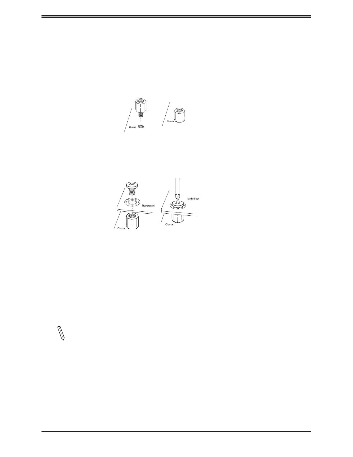
2.2 Motherboard Installation
All motherboards have standard mounting holes to fi t different types of chassis. Make sure
that the locations of all the mounting holes for both the motherboard and the chassis match.
Although a chassis may have both plastic and metal mounting fasteners, metal ones are
highly recommended because they ground the motherboard to the chassis. Make sure that
the metal standoffs click in or are screwed in tightly.
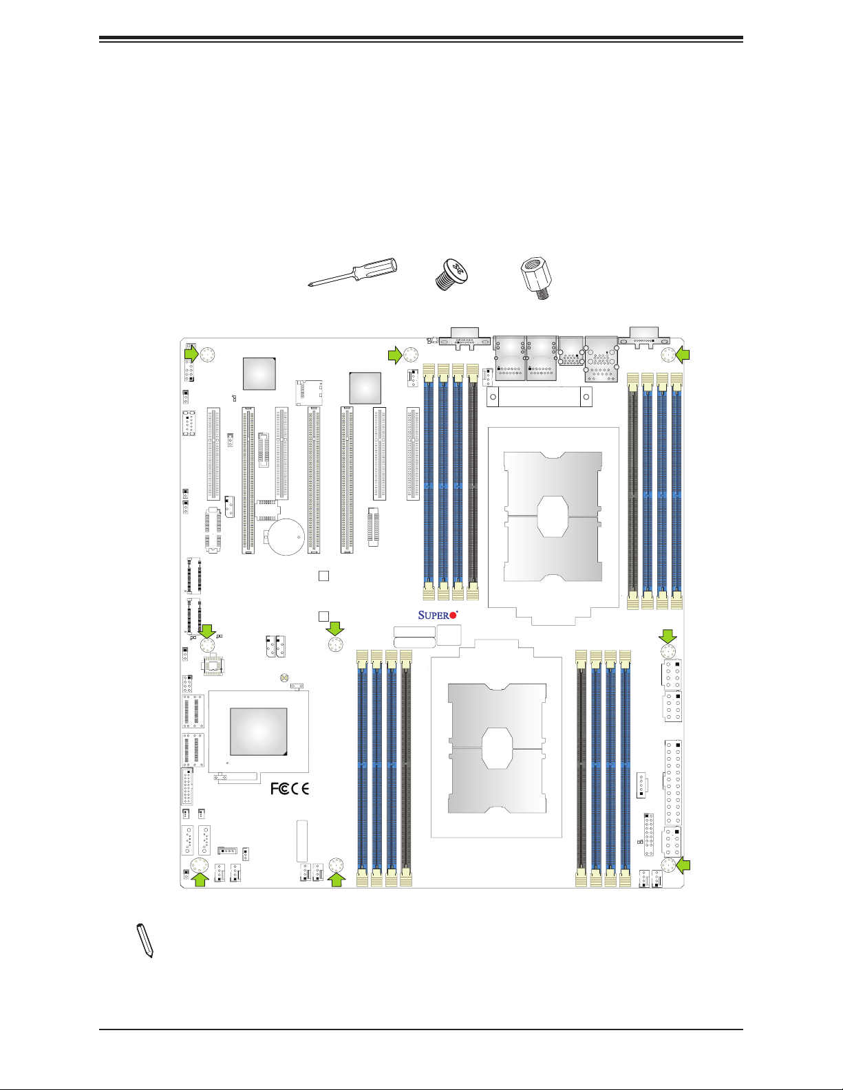
Tools Needed
JTPM1
JPME2
CPU1 SLOT1 PCI-E 3.0 x8
USB 6 (3.0)
JD1
JP4
M.2-C1
M.2-C2
LE4
JWD1
T-SGPIO1
BIOS
I-S ATA 0~3
BMC
LEDM1
ASPEED
AST2500
CPU2 SLOT2 PCI-E 3.0 x16
JNCSI
JIPMB1
+
LE3
JSDCARD1
CPU1 SLOT3 PCI-E 3.0 x8
CPU2 SLOT4 PCI-E 3.0 x16
Battery
BT1
MH4
MH11
JBT1
LAN
CTRL
CPU2 SLOT5 PCI-E 3.0 x16
CPU1 SLOT6 PCI-E 3.0 x8
CPU1-HSSI GPIO
JHSSI
P1-DIMMD2
P1-DIMMD1
P1-DIMME1
P1-DIMMF1
Screws (9)
LE1
JUIDB1
VGA
FAN6
CPU1 SLOT7 PCI-E 3.0 x8
P2-DIMMA2
P2-DIMMA1
P2-DIMMB1
P2-DIMMC1
X11DPH-i
MAC CODE
BAR CODE
REV: 1.10
BIOS LICENSE
Standoffs (9) as Needed
USB 2/3(3.0)
FAN5
LAN1
LAN2
CPU2
IPMI_LAN
USB 0/1(3.0)
P1-DIMMA1
P1-DIMMA2
P1-DIMMC1
P1-DIMMB1
P2-DIMMD2
COM1
P2-DIMMD1
P2-DIMME1
JPWR4
JPWR2
P2-DIMMF1
I-S ATA 4~7
Intel
PCH
CPU1
JSD1
SATA2
JL1
USB 4/5(3.0)
JSD2
S-SATA0
S-SATA1
SATA1
FANB
JRK1
FANA
IPMI CODE
JSTBY1
FAN4 FAN3
JPI2C1
LE2
FAN2
JPWR3
JF1
JPWR1
FAN1
Location of Mounting Holes
Notes: 1. To avoid damaging the motherboard and its components, please do not use
a force greater than 8 lb/inch on each mounting screw during motherboard installation.
2. Some components are very close to the mounting holes. Please take precautionary
measures to avoid damaging these components when installing the motherboard to
the chassis.
23
Page 24
Super X11DPH-i/X11DPH-T/X11DPH-Tq User's Manual
Installing the Motherboard
1. Install the I/O shield into the back of the chassis if needed.
2. Locate the mounting holes on the motherboard. See the previous page for the location.
3. Locate the matching mounting holes on the chassis. Align the mounting holes on the
motherboard against the mounting holes on the chassis.
4. Install standoffs in the chassis as needed.
5. Install the motherboard into the chassis carefully to avoid damaging other motherboard
components.
6. Using the Phillips screwdriver, insert a Pan head #6 screw into a mounting hole on the
motherboard and its matching mounting hole on the chassis.
7. Repeat Step 5 to insert Pan head #6 screws into all mounting holes.
8. Make sure that the motherboard is securely placed in the chassis.
Note: Images displayed in this manual are for illustration only. Your chassis or
components might look different from those shown in this manual.
24
Page 25

Chapter 2: Installation
2.3 Processor and Heatsink Installation
Warning: When handling the processor package, avoid placing direct pressure on the label
area of the CPU or CPU socket. Also, improper CPU installation or socket misalignment can
cause serious damage to the CPU or motherboard which may result in RMA repairs. Please
read and follow all instructions thoroughly before installing your CPU and heatsink.
Notes:
• Always connect the power cord last, and always remove it before adding, removing, or
changing any hardware components. Please note that the processor and heatsink should
be assembled together fi rst to form the Processor Heatsink Module (PHM), and then install
the entire PHM into the CPU socket.
• When you receive a motherboard without a processor pre-installed, make sure that the
plastic CPU socket cap is in place and that none of the socket pins are bent; otherwise,
contact your retailer immediately.
• Refer to our website at www.Supermicro.com for CPU support updates.
• Please follow the instructions given in the ESD Warning section on the fi rst page of this
chapter before handling, installing, or removing system components.
Intel Xeon Scalable-SP and 2nd Gen Intel Xeon Scalable-SP
Processors
Note: All graphics, drawings, and pictures shown in this manual are for illustration only.
The components that came with your system may or may not look exactly the same
as those shown in this manual.
25
Page 26
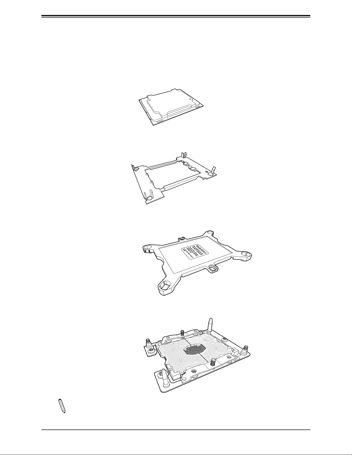
Super X11DPH-i/X11DPH-T/X11DPH-Tq User's Manual
Overview of the Processor Socket Assembly
The processor socket assembly contains 1) the Intel Xeon Scalable-SP or
2nd Generation Intel Xeon Scalable-SP processor, 2) the narrow processor clip, 3) the dust
cover, and 4) the CPU socket.
1. Intel Processor
2. Narrow processor clip (the plastic processor package carrier used for the CPU)
3. Dust Cover
4. CPU Socket
Note: Be sure to cover the CPU socket with the dust cover when the CPU is not in-
stalled.
26
Page 27
Chapter 2: Installation
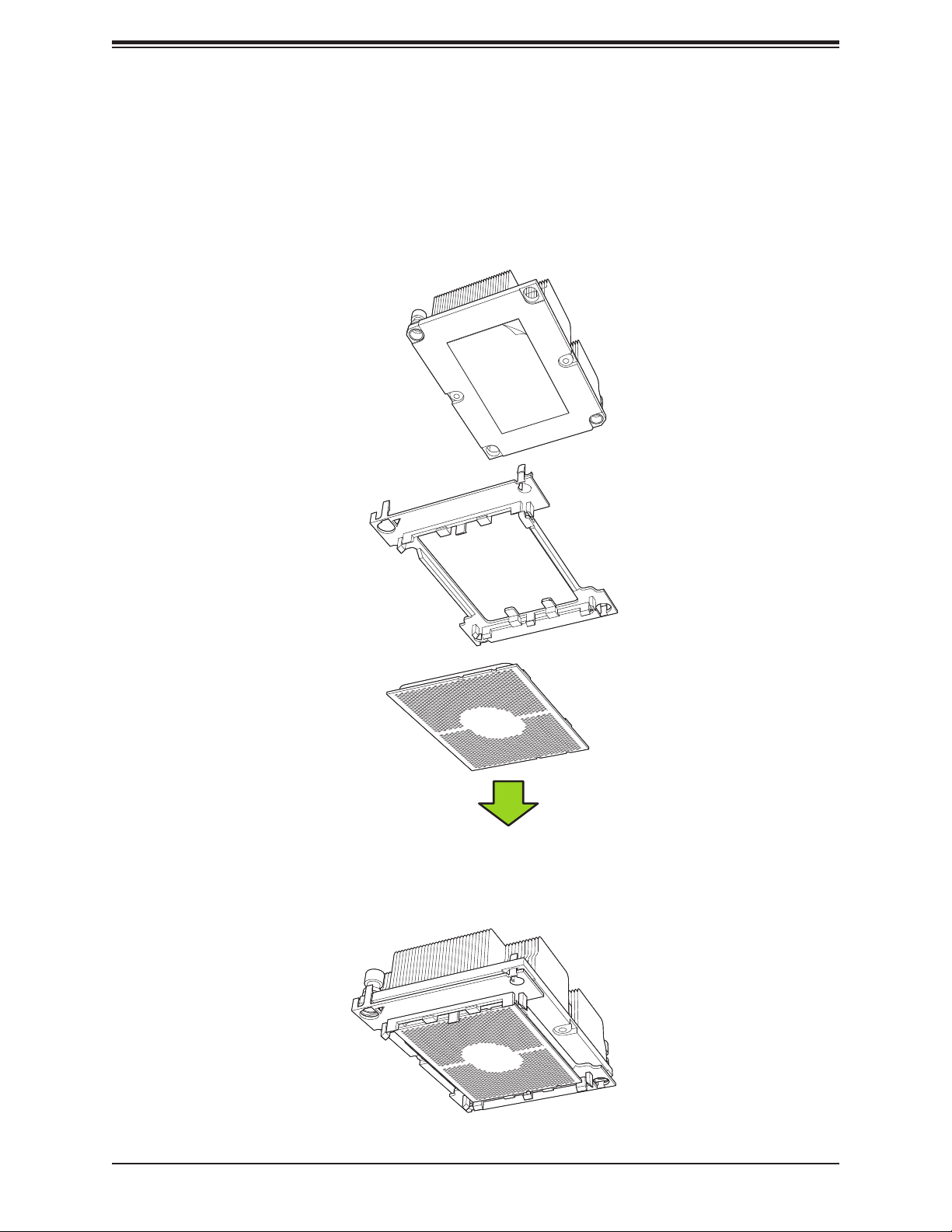
Overview of the Processor Heatsink Module (PHM)
The Processor Heatsink Module (PHM) contains 1) a heatsink, 2) a narrow processor clip,
and 3) Intel Xeon Scalable-SP or 2nd Generation Intel Xeon Scalable-SP processor.
1. Heatsink
2. Narrow processor clip
3. Intel Processor
Processor Heatsink Module (PHM)
(Bottom View)
27
Page 28
Super X11DPH-i/X11DPH-T/X11DPH-Tq User's Manual
Attaching the Processor to the Narrow Processor Clip to Create
the Processor Package Assembly
To properly install the CPU into the narrow processor clip, please follow the steps below.
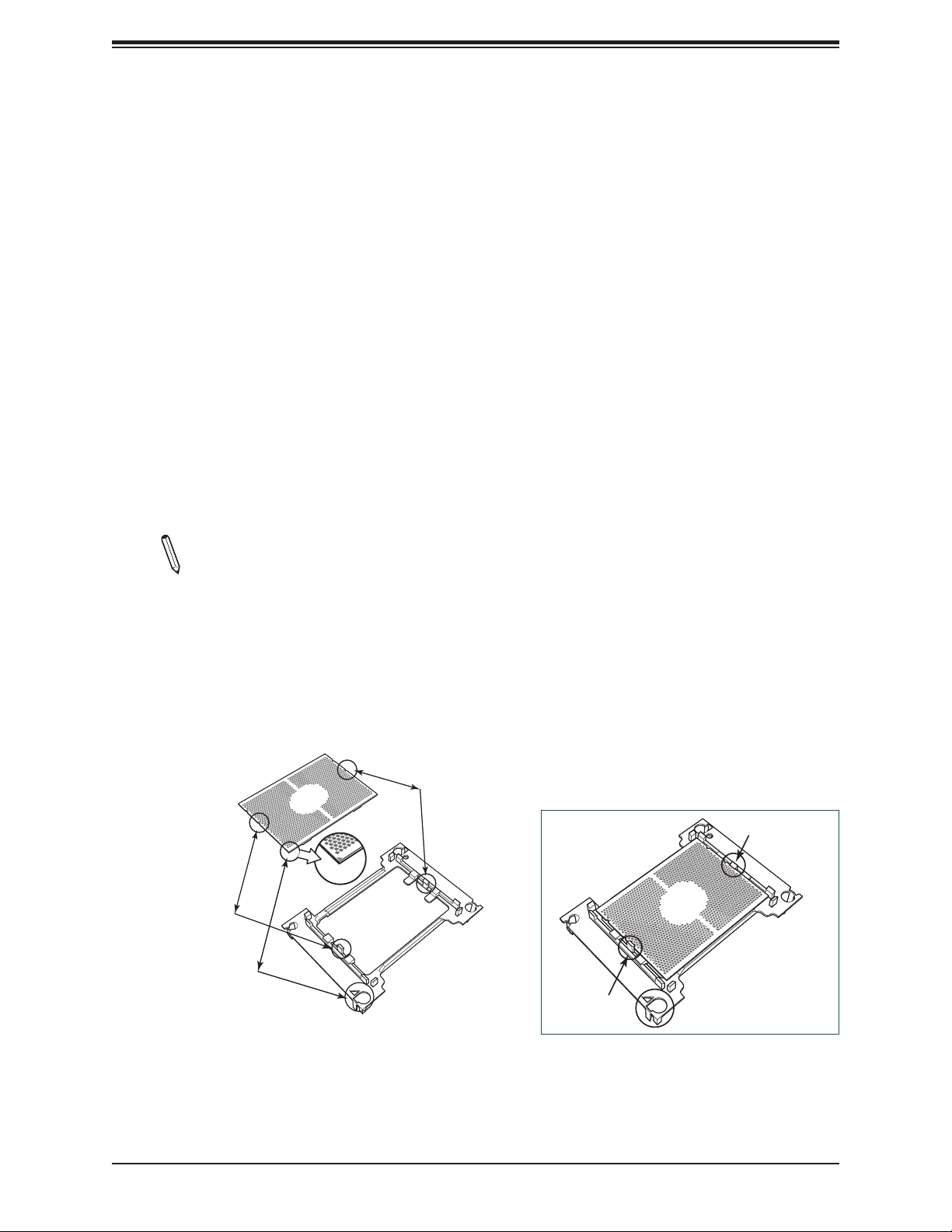
1. Locate pin 1 (notch A), which is the triangle located on the top of the narrow processor
clip. Also locate notch B and notch C on the processor clip.
2. Locate pin 1 (notch A), which is the triangle on the substrate of the CPU. Also, locate
notch B and notch C on the CPU as shown below.
3. Align pin 1 (the triangle on the substrate) of the CPU with pin 1 (the triangle) of
the narrow processor clip. Once they are aligned, carefully insert the CPU into the
processor clip by sliding notch B of the CPU into notch B of the processor clip, and
sliding notch C of the CPU into notch C of the processor clip.
4. Examine all corners of the CPU to ensure that it is properly seated on the processor
clip. Once the CPU is securely attached to the processor clip, the processor package
assembly is created.
Note: Please exercise extreme caution when handling the CPU. Do not touch the
CPU LGA-lands to avoid damaging the LGA-lands or the CPU. Be sure to wear ESD
gloves when handling components.
CPU (Upside Down)
w/CPU LGA Lands up
Align Notch B of the CPU
and Notch B of the Processor Clip
Align CPU Pin 1
C
Align Notch C of the CPU
and Notch C of the Processor Clip
B
Allow Notch C to
latch on to CPU
A
Pin 1
C
C
B
CPU/Heatsink Package
(Upside Down)
A
Allow Notch B to
latch on to CPU
B
A
Processor Package Carrier (w/CPU mounted
on the Processor Clip)
28
Page 29
Chapter 2: Installation
Attaching the Processor Package Assembly to the Heatsink to
Form the Processor Heatsink Module (PHM)
After you have made a processor package assembly by following the instructions on the
previous page, please follow the steps below to mount the processor package assembly onto
the heatsink to create the Processor Heatsink Module (PHM).
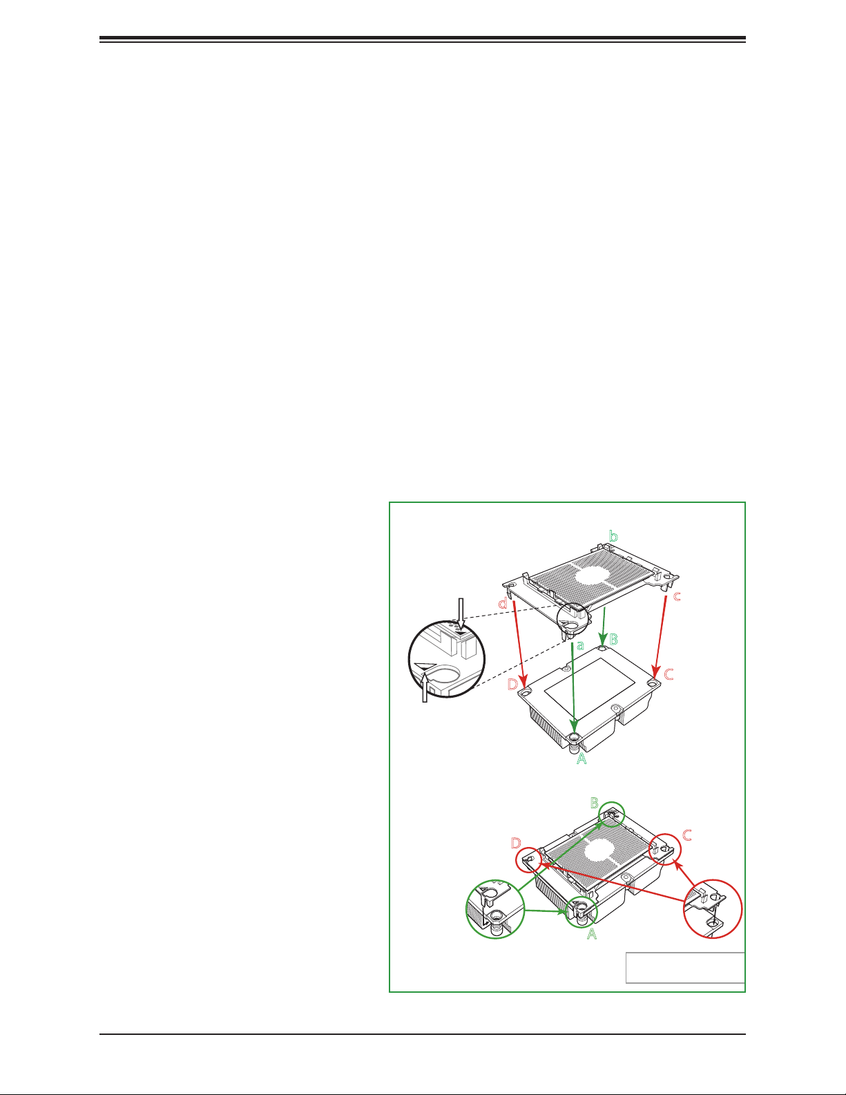
1. Locate "1" on the heatsink label and the triangular corner next to it on the heatsink.
With your index fi nger pressing against the screw at this triangular corner, carefully hold
and turn the heatsink upside down with the thermal-grease side facing up. Remove the
protective thermal fi lm if present, and apply the proper amount of the thermal grease
as needed. (Skip this step if you have a new heatsink because the necessary thermal
grease is pre-applied in the factory.)
2. Holding the processor package assembly at the center edge, turn it upside down. With
the thermal-grease side facing up, locate the hollow triangle located at the corner of the
processor carrier assembly ("a" in the graphic). Note a larger hole and plastic mounting
clicks located next to the hollow triangle. Also locate another set of mounting clicks and
a larger hole at the diagonal corner
of the same (reverse) side of the
processor carrier assembly ("b" in
the graphic).
3. With the back of heatsink and
the reverse side of the processor
package assembly facing up, align
the triangular corner on the heatsink
("A" in the graphic) against the
mounting clips next to the hollow
triangle ("a") on the processor
package assembly.
4. Also align the triangular corner ("B")
at the diagonal side of the heatsink
with the corresponding clips on the
processor package assembly ("b").
Triangle on the CPU
Triangle on the
Processor Clip
Non-Fabric CPU and Processor Clip
(Upside Down)
b
d
B
a
D
Heatsink
(Upside Down)
A
On Locations of (C, D), the notches
snap onto the heat sink’s
B
c
C
mounting holes
5. Once the mounting clips on the
processor package assembly
are properly aligned with the
corresponding holes on the back
of heatsink, securely attach the
heatsink to the processor package
assembly by snapping the mounting
clips at the proper places on the
heatsink to create the processor
heatsink module (PHM).
29
D
A
On Locations (A, B), the notches
snap onto the heatsink’s sides
C
Make sure Mounting
Notches snap into place
Page 30
Super X11DPH-i/X11DPH-T/X11DPH-Tq User's Manual
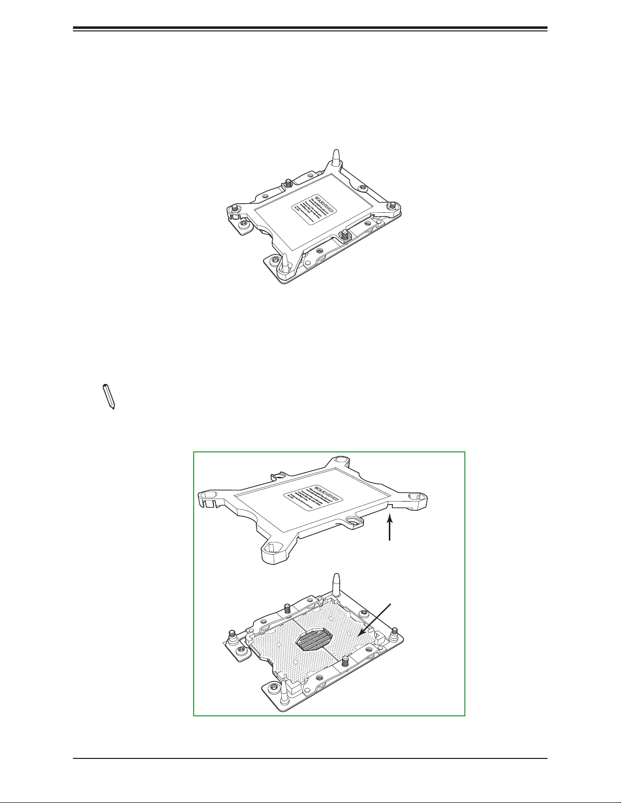
Preparing the CPU Socket for Installation
This motherboard comes with the CPU socket pre-assembled in the factory. The CPU socket
contains 1) a dust cover, 2) a socket bracket, 3) the CPU (P0) socket, and 4) a back plate.
These components are pre-installed on the motherboard before shipping.
CPU Socket w/Dust Cover On
Removing the Dust Cover from the CPU Socket
Remove the dust cover from the CPU socket, exposing the CPU socket and socket pins as
shown on the illustration below.
Note: Do not touch the socket pins to avoid damaging them, causing the CPU to
malfunction.
Dusk Cover
Remove the dust cover from
the CPU socket. Do not
touch the socket pins!
Socket Pins
CPU Socket
30
Page 31

Chapter 2: Installation
Installing the Processor Heatsink Module (PHM)
1. Once you have assembled the processor heatsink module (PHM), you are ready to
install the processor heatsink module (PHM) into the CPU socket on the motherboard.
To install the PHM into the CPU socket, follow the instructions below.
2. Locate the triangle (pin 1) on the CPU socket, and locate the triangle (pin 1) at the
corner of the PHM that is closest to "1." (If you have diffi culty locating pin 1 of the PHM,
turn the PHM upside down. With the LGA-lands side facing up, you will note the hollow
triangle located next to a screw at the corner. Turn the PHM right side up, and you will
see a triangle marked on the processor clip at the same corner of hollow triangle.)
3. Carefully align pin 1 (the triangle) on the PHM against pin 1 (the triangle) on the CPU
socket.
4. Once they are properly aligned, insert the two diagonal oval holes on the heatsink into
the guiding posts.
5. Using a T30 Torx-bit screwdriver, install four screws into the mounting holes on the
socket to securely attach the PHM onto the motherboard starting with the screw marked
"1" (in the sequence of 1, 2, 3, and 4).
Note: Do not use excessive force when tightening the screws to avoid damaging the
LGA-lands and the processor.
31
Page 32

Super X11DPH-i/X11DPH-T/X11DPH-Tq User's Manual
Removing the Processor Heatsink Module (PHM) from the
Motherboard
Before removing the processor heatsink module (PHM), unplug power cord from the power
outlet.
1. Using a T30 Torx-bit screwdriver, turn the screws on the PHM counterclockwise to
loosen them from the socket, starting with screw marked #4 (in the sequence of 4, 3, 2,
1).
2. After all four screws are removed, wiggle the PHM gently and pull it up to remove it
from the socket.
Note: To properly remove the processor heatsink module, be sure to loosen and remove the screws on the PHM in the sequence of 4, 3, 2, 1 as shown below.
#1
Removing the screws in
the sequence of 4, 3, 2, 1
#4
#2
#3
Printed Triangle on Motherboard
CPU Socket
After removing the screws,
lift the Processor Heatsink
Module off the CPU socket.
32
Page 33

Chapter 2: Installation
2.4 Memory Support and Installation
Note: Check Supermicro's website for recommended memory modules. Exercise ex-
treme care when installing or removing DIMM modules to prevent any damage.
Memory Support
The motherboard supports up to 4TB of 3DS Load Reduced DIMM (3DS LRDIMM), Load
Reduced DIMM (LRDIMM), 3DS Registered DIMM (3DS RDIMM), Registered DIMM (RDIMM),
Non-Volatile DIMM (NV-DIMM) DDR4 (288-pin) ECC 2933*/2666/2400/2133 MHz memory
in 16 slots (*Note below). This motherboard also supports up to 5TB memory with DCPMM
modules installed based on the DCPMM population table on page 38.
Notes: 1. 2933 MHz memory is supported by 2nd Gen Intel Xeon Scalable-SP
(82xx/62xx series) processors only. 2. Populating DDR4 memory modules in a twoDIMMs per-channel (2DPC) confi guration on this motherboard will affect memory
bandwidth and performance.
Memory Installation Sequence
Memory modules for this motherboard are populated using the "Fill First" method. The blue
memory slot of each channel is considered the "fi rst DIMM module" of the channel, and the
black slot, the second module of the channel. When installing memory modules, be sure to
populate the blue memory slots fi rst and then populate the black slots.
General Memory Population Requirements
1. Be sure to use the memory modules of the same type and the same speed on the same
motherboard. Mixing of memory modules of different types and speeds is not allowed.
2. Using unbalanced memory topology such as populating two DIMMs in one channel while
populating one DIMM in another channel on the same motherboard will result in reduced
memory performance.
3. Populating memory slots with a pair of DIMM modules of the same type and size will
result in interleaved memory, which will improve memory performance.
33
Page 34

Super X11DPH-i/X11DPH-T/X11DPH-Tq User's Manual
DDR4 Memory Support for Intel Xeon Scalable-SP Processors
DDR4 Memory Support
Type
RDIMM SRx4 4GB 8GB 2666 2666 2666
RDIMM SRx8 8GB 16GB 2666 2666 2666
RDIMM DRx8 8GB 16GB 2666 2666 2666
RDIMM DRx4 16GB 32GB 2666 2666 2666
RDIMM 3Ds QRX4 N/A 2H-64GB 2666 2666 2666
RDIMM 3Ds 8RX4 N/A 4H-128GB 2666 2666 2666
LRDIMM QRx4 32GB 64GB 2666 2666 2666
LRDIMM 3Ds QRX4 N/A 2H-64GB 2666 2666 2666
LRDIMM 3Ds 8Rx4 N/A 4H-128GB 2666 2666 2666
Ranks Per
DIMM & Data
Width
DIMM Capacity (GB)
DRAM Density
4Gb* 8Gb 1.2 V 1.2 V 1.2 V
Speed (MT/s); Voltage (V); Slots Per Channel (SPC) and DIMMs Per Channel
1 Slot Per Channel 2 Slots Per Channel
1DPC (1-DIMM
Per Channel)
(DPC)
1DPC (1-DIMM Per
Channel)
2DPC (2-DIMM Per
Channel)
DDR4 Memory Support for 2nd Gen Intel Xeon Scalable-SP
Processors
DDR4 Memory Support
Ranks
Type
RDIMM SRx4 4GB 8GB 16GB 2933 2933 2933
RDIMM SRx8 8GB 16GB 32GB 2933 2933 2933
RDIMM DRx8 8GB 16GB 32GB 2933 2933 2933
RDIMM DRx4 16GB 32GB 64GB 2933 2933 2933
RDIMM 3Ds QRX4 N/A 2H-64GB 2H-128GB 2933 2933 2933
RDIMM 3Ds 8RX4 N/A 4H-128GB 4H-256GB 2933 2933 2933
LRDIMM QRx4 32GB 64GB 128GB 2933 2933 2933
LRDIMM 3Ds QRX4 N/A 2H-64GB 2H-128GB 2933 2933 2933
LRDIMM 3Ds 8Rx4 N/A 4H-128GB 4H-256GB 2933 2933 2933
Per DIMM
&
Data Width
DIMM Capacity (GB)
DRAM Density
4Gb* 8Gb 16Gb 1.2 V 1.2 V 1.2 V
Speed (MT/s); Voltage (V); Slots Per Channel (SPC) and DIMMs Per Chan-
1 Slot Per Channel 2 Slots Per Channel
1DPC (1-DIMM
Per Channel)
nel (DPC)
1DPC (1-DIMM
Per Channel)
2DPC (2-DIMM
Per Channel)
Notes: 1. 2933 MHz memory support in two-DIMMs per-channel (2DPC) confi guration
can be achieved by using memory purchased from Supermicro. 2. 2933 MHz memory
is supported by 2nd Gen Intel Xeon Scalable-SP (82xx/62xx series) processors only.
34
Page 35

Chapter 2: Installation
DIMM Population Guidelines for Optimal Performance
For optimal memory performance, follow the instructions listed in the tables below when
populating memory modules.
Key Parameters for DIMM Confi guration
Key Parameters for DIMM Confi gurations
Parameters Possible Values
Number of Channels 1, 2, 3, 4, 5, or 6
Number of DIMMs per Channel 1DPC (1 DIMM Per Channel) or 2DPC (2 DIMMs Per Channel)
DIMM Type RDIMM (w/ECC), 3DS RDIMM, LRDIMM, 3DS LRDIMM
DIMM Construction non-3DS RDIMM Raw Cards: A/B (2Rx4), C (1Rx4), D (1Rx8), E (2Rx8)
DIMM Mixing Guidelines
3DS RDIMM Raw Cards: A/B (4Rx4)
non-3DS LRDIMM Raw Cards: D/E (4Rx4)
3DS LRDIMM Raw Cards: A/B (8Rx4)
General DIMM Mixing Guidelines
DIMM Mixing Rules
• All DIMMs must be all DDR4 DIMMs.
• x4 and x8 DIMMs can be mixed in the same channel.
• Mixing of LRDIMMs and RDIMMs is not allowed in the same channel, across different channels, and across
different sockets.
• Mixing of non-3DS and 3DS LRDIMM is not allowed in the same channel, across different channels, and across
different sockets.
Mixing of DIMM Types within a Channel
DIMM Types
RDIMM Allowed Not Allowed Not Allowed
LRDIMM Not Allowed Allowed Not Allowed
3DS LRDIMM Not Allowed Not Allowed Allowed
RDIMM LRDIMM 3DS LRDIMM
35
Page 36

Super X11DPH-i/X11DPH-T/X11DPH-Tq User's Manual
DIMM Population Table
Note. Unbalanced memory confi guration decreases memory performance and is not
recommended for Supermicro motherboards.
DDR4 Memory Population Table for the Motherboard Using Intel Xeon
Scalable-SP and 2nd Gen Intel Xeon Scalable-SP Processors
Memory Population Table for the X11DP Motherboard w/16 DIMM Slots Onboard
When 1 CPU is used: Memory Population Sequence
1 CPU & 1 DIMM CPU1: P1-DIMMA1
1 CPU & 2 DIMMs CPU1: P1-DIMMA1/P1-DIMMD1
1 CPU & 3 DIMMs CPU1: P1-DIMMC1/P1-DIMMB1/P1-DIMMA1
1 CPU & 4 DIMMs CPU1: P1-DIMMB1/P1-DIMMA1/P1-DIMMD1/P1-DIMME1
1 CPU & 5 DIMMs
(Unbalanced: not recommended)
1 CPU & 6 DIMM CPU1: P1-DIMMC1/P1-DIMMB1/P1-DIMMA1/P1-DIMMD1/P1-DIMME1/P1-DIMMF1
1 CPU & 7 DIMMs
(Unbalanced: not recommended)
1 CPU & 8 DIMMs
(Unbalanced: not recommended)
When 2 CPUs are used: Memory Population Sequence
2 CPUs & 2 DIMMs
2 CPUs & 4 DIMMs
2 CPUs & 6 DIMMs
2 CPUs & 8 DIMMs
2 CPUs & 10 DIMMs
2 CPUs & 12 DIMMs
2 CPUs & 14 DIMMs
(Unbalanced: not recommended)
2 CPUs & 16 DIMMs
(Unbalanced: not recommended)
CPU1: P1-DIMMC1/P1-DIMMB1/P1-DIMMA1/P1-DIMMD1/P1-DIMME1
CPU1:P1-DIMMC1/P1-DIMMB1/P1-DIMMA1/P1-DIMMA2/P1-DIMMD1/P1-DIMME1/P1-DIMMF1
CPU1: P1-DIMMC1/P1-DIMMB1/P1-DIMMA1/P1-DIMMA2/P1-DIMMD2/P1-DIMMD1/P1-DIMME1/P1-DIMMF1
CPU1: P1-DIMMA1
CPU2: P2-DIMMA1
CPU1: P1-DIMMA1/P1-DIMMD1
CPU2: P2-DIMMA1/P2-DIMMD1
CPU1: P1-DIMMC1/P1-DIMMB1/P1-DIMMA1
CPU2: P2-DIMMC1/P2-DIMMB1/P2-DIMMA1
CPU1: P1-DIMMB1/P1-DIMMA1/P1-DIMMD1/P1-DIMME1
CPU2: P2-DIMMB1/P2-DIMMA1/P2-DIMMD1/P2-DIMME1
CPU1: P1-DIMMC1/P1-DIMMB1/P1-DIMMA1/P1-DIMMD1/P1-DIMME1/P1-DIMMF1
CPU2: P2-DIMMB1/P2-DIMMA1/P2-DIMMD1/P2-DIMME1
CPU1: P1-DIMMC1/P1-DIMMB1/P1-DIMMA1/P1-DIMMD1/P1-DIMME1/P1-DIMMF1
CPU2: P2-DIMMC1/P2-DIMMB1/P2-DIMMA1/P2-DIMMD1/P2-DIMME1/P2-DIMMF1
CPU1: P1-DIMMC1/P1-DIMMB1/P1-DIMMA1/P1-DIMMA2/P1-DIMMD1/P1-DIMME1/P1-DIMMF1
CPU2: P2-DIMMC1/P2-DIMMB1/P2-DIMMA1/P2-DIMMA2/P2-DIMMD1/P2-DIMME1/P2-DIMMF1
CPU1: P1-DIMMC1/P1-DIMMB1/P1-DIMMA1/P1-DIMMA2/P1-DIMMD2/P1-DIMMD1/P1-DIMME1/P1-DIMMF1
CPU2: P2-DIMMC1/P2-DIMMB1/P2-DIMMA1/P2-DIMMA2/P2-DIMMD2/P2-DIMMD1/P2-DIMME1/P2-DIMMF1
Note: Please refer to the Memory Confi guration User Guide for the X11 UP/DP/MP
Motherboards that is posted on our website for detailed information on memory support for this motherboard.
36
Page 37

Chapter 2: Installation
DCPMM Memory Population Tables for 2nd Gen Intel Xeon Scalable-SP
Processors
Note: Only 2nd Gen Intel Xeon Scalable-SP (82xx/62xx/52xx/42xx series) processors
support DCPMM memory.
Symmetric Population within 1 CPU Socket
Modes P1-DIMMF1 P1-DIMME1 P1-DIMMD1 P1-DIMMD2 P1-DIMMA2 P1-DIMMA1 P1-DIMMB1 P1-DIMMC1 Channel Confi g.
AD DRAM1 DRAM1 DRAM1 DCPMM DCPMM DRAM1 DRAM1 DRAM1 2-1-1
MM DRAM2 DRAM2 DRAM2 DCPMM DCPMM DRAM2 DRAM2 DRAM2 2-1-1
AD + MM DRAM3 DRAM3 DRAM3 DCPMM DCPMM DRAM3 DRAM3 DRAM3 2-1-1
AD DCPMM DRAM1 DRAM1 - - DRAM1 DRAM1 DCPMM 1-1-1
MM DCPMM DRAM1 DRAM1 - - DRAM1 DRAM1 DCPMM 1-1-1
AD + MM DCPMM DRAM3 DRAM3 - - DRAM3 DRAM3 DCPMM 1-1-1
Asymmetric Population within 1 CPU Socket
Modes P1-DIMMF1 P1-DIMME1 P1-DIMMD1 P1-DIMMD2 P1-DIMMA2 P1-DIMMA1 P1-DIMMB1 P1-DIMMC1 Channel Confi g.
AD DRAM1 DRAM1 DRAM1 - DCPMM DRAM1 DRAM1 DRAM1 2-1-1
AD* DRAM1 DRAM1 DRAM1 - DCPMM DRAM1 DRAM1 DRAM1 2-1-1
(for the two tables above)
DDR4 Type Capacity
DRAM1 RDIMM 3DS RDIMM LRDIMM 3DS LRDIMM
DRAM2 RDIMM - - -
DRAM3 RDIMM 3DS RDIMM LRDIMM -
Note: DDR4 single rank x8 is not available for DCPMM Memory Mode or App-Direct Mode.
DCPMM Any Capacity (Uniformly for all channels for a given confi guration)
Legend
Refer to Validation Matrix (DDR4 DIMMs validated with
Legend
(for the fi rst two tables above)
Capacity
DCPMM) below.
• * 2nd socket has no DCPMM DIMM
• For MM, general NM/FM ratio is between 1:4 and 1:16. Excessive capacity for FM can be used for AD. (NM = Near
Memory; FM = Far Memory)
• For each individual population, rearrangements between channels are allowed as long as the resulting population is
compliant with the memory rules for 2nd Gen Intel Xeon Scalable-SP (82xx/62xx/52xx/42xx series) processors.
• For each individual population, please use the same DDR4 DIMM in all slots.
• For each individual population, sockets are normally symmetric with exceptions for 1 DCPMM per socket and 1 DCPMM
per node case. Currently, DCPMM modules operate at 2666 MHz.
• No mixing of DCPMM and NVMDIMMs within the same platform is allowed.
• These DCPMM population tables target a balanced DCPMM-to-DRAM-cache ratio in MM and MM + AD modes.
Validation Matrix (DDR4 DIMMs Validated w/DCPMM)
DIMM Type
RDIMM
LRDIMM 4Rx4 N/A 64GB
LRDIMM 3DS 8Rx4 (4H) N/A 128GB
Ranks Per DIMM
& Data Width
(Stack)
1Rx4 8GB 16GB
2Rx8 8GB 16GB
2Rx4 16GB 32GB
DIMM Capacity (GB)
DRAM Density
4Gb 8Gb
37
Page 38

Super X11DPH-i/X11DPH-T/X11DPH-Tq User's Manual
DIMM Installation
1. Follow the instructions given in the
memory population tables provided in the
previous section to install memory modules
on your motherboard. For the system
to work properly, please use memory
modules of the same type and speed on
the motherboard.
2. Push the release tabs outwards on both
ends of the DIMM slot to unlock it.
3. Align the key of the DIMM module with the
receptive point on the memory slot.
4. Align the notches on both ends of the
module against the receptive points on the
ends of the slot.
5. Use two thumbs together to press both
ends of the module straight down into the
slot until the module snaps into place.
JWD1
T-SGPIO1
JPME2
USB 6 (3.0)
JD1
JP4
M.2-C1
M.2-C2
LE4
JSD1
SATA2
JL1
JTPM1
USB 4/5(3.0)
S-SATA1
BMC
LEDM1
ASPEED
AST2500
CPU2 SLOT2 PCI-E 3.0 x16
CPU1 SLOT1 PCI-E 3.0 x8
JIPMB1
LE3
BIOS
I-SATA 0 ~3
Intel
I-SATA 4 ~7
PCH
JSD2
S-SATA0
JSTBY1
SATA1
JRK1
FANA
FANB
JSDCARD1
CPU1 SLOT3 PCI-E 3.0 x8
CPU2 SLOT4 PCI-E 3.0 x16
JNCSI
Battery
+
BT1
JBT1
IPMI CODE
FAN4 FA N3
CPU2 SLOT5 PCI-E 3.0 x16
MH4
MH11
P1-DIMMD2
P1-DIMMD1
P1-DIMME1
P1-DIMMF1
LAN
CTRL
CPU1 SLOT6 PCI-E 3.0 x8
CPU1-HSSI GPIO
JHSSI
LE1
JUIDB1
FAN6
CPU1 SLOT7 PCI-E 3.0 x8
P2-DIMMA2
P2-DIMMA1
P2-DIMMB1
P2-DIMMC1
MAC CODE
BIOS LICENSE
BAR CODE
VGA
X11DPH-i
REV: 1.10
USB 2/3(3.0)
FAN5
LAN1
LAN2
CPU2
CPU1
P1-DIMMA2
IPMI_LAN
USB 0/1(3.0)
P1-DIMMA1
P1-DIMMB1
P2-DIMMD2
P1-DIMMC1
FAN2
COM1
LE2
P2-DIMMD1
JPWR4
JPWR2
JPWR3
JF1
JPWR1
P2-DIMME1
FAN1
P2-DIMMF1
6. Press the release tabs to the lock positions
Notches
to secure the DIMM module into the slot.
Release Tabs
DIMM Module Removal
Press the release tabs on both ends of the DIMM socket to release the DIMM module from
the socket as shown in the drawing on the right.
Warnings: 1. Please do not use excessive force when pressing the release tabs on the ends
of the DIMM socket to avoid causing any damage to the DIMM module or the DIMM socket.
2. Please handle DIMM modules with care. Carefully follow all the instructions given on Page
1 of this chapter to prevent ESD-related damages to your memory modules or components.
38
Page 39

Chapter 2: Installation
2.5 Rear I/O Ports
See the drawings below for the locations and descriptions of the various I/O ports on the
rear side of your system.
M.2-C1
M.2-C2
LE4
JWD1
T-SGPIO1
JTPM1
JPME2
USB 6 (3.0)
JD1
JP4
USB 4/5(3.0)
JSD1
S-SATA1
SATA2
JL1
BMC
LEDM1
ASPEED
AST2500
CPU2 SLOT2 PCI-E 3.0 x16
CPU1 SLOT1 PCI-E 3.0 x8
JIPMB1
LE3
BIOS
I-SATA 0~3
Intel
I-SATA 4~7
PCH
JSD2
S-SATA0
JSTBY1
SATA1
JRK1
FANA
FANB
JSDCARD1
CPU1 SLOT3 PCI-E 3.0 x8
CPU2 SLOT4 PCI-E 3.0 x16
JNCSI
Battery
+
BT1
JBT1
IPMI CODE
FAN4 FAN3
CPU2 SLOT5 PCI-E 3.0 x16
MH4
MH11
P1-DIMMD2
P1-DIMMD1
P1-DIMME1
P1-DIMMF1
LAN
CTRL
CPU1 SLOT7 PCI-E 3.0 x8
CPU1 SLOT6 PCI-E 3.0 x8
CPU1-HSSI GPIO
JHSSI
MAC CODE
BAR CODE
FAN6
P2-DIMMA2
P2-DIMMA1
P2-DIMMB1
P2-DIMMC1
LE1
JUIDB1
VGA
FAN5
X11DPH-i
REV: 1.10
BIOS LICENSE
CPU1
USB 2/3(3.0)
LAN1
LAN2
CPU2
IPMI_LAN
USB 0/1(3.0)
P1-DIMMA2
P1-DIMMA1
P1-DIMMB1
COM1
P2-DIMMD2
P1-DIMMC1
FAN2
P2-DIMMD1
JF1
LE2
P2-DIMME1
JPWR4
JPWR2
JPWR3
JPWR1
FAN1
P2-DIMMF1
Back panel I/O Port Locations and Defi nitions
4
6
1
3
5
7
98
10
2
Back Panel I/O Ports
No. Description No. Description
1. COM1 6. USB 3 (USB 3.0)
2. USB 0 (USB 3.0) 7. GLAN1 (X11DPH-i), 10G_LAN1 (X11DPH-T/X11DPH-Tq)
3. USB 1 (USB 3.0) 8. GLAN2 (X11DPH-i), 10G_LAN2 (X11DPH-T/X11DPH-Tq)
4. IPMI LAN 9. VGA
5. USB 2 (USB 3.0) 10. Unit Identifi er Switch (UID)
39
Page 40

Super X11DPH-i/X11DPH-T/X11DPH-Tq User's Manual
VGA Port
The onboard VGA port is located next to IPMI LAN port on the I/O back panel. Use this
connection for VGA display.
Serial Port
There is one COM port (COM1) on the I/O back panel on the motherboard. The COM port
provides serial communication support. See the table below for pin defi nitions.
Pin# Defi nition Pin# Defi nition
1 DCD 6 DSR
2 RXD 7 RTS
3 TXD 8 CTS
4 DTR 9 RI
5 Ground 10 N/A
LE4
JWD1
T-SGPIO1
JTPM1
JPME2
USB 6 (3.0)
JD1
JP4
M.2-C1
M.2-C2
USB 4/5(3.0)
JSD1
S-SATA1
SATA2
JL1
BMC
LEDM1
ASPEED
AST2500
CPU2 SLOT2 PCI-E 3.0 x16
CPU1 SLOT1 PCI-E 3.0 x8
JIPMB1
LE3
BIOS
I-SATA 0~3
Intel
I-SATA 4~7
PCH
JSD2
S-SATA0
JSTBY1
SATA1
JRK1
FANA
FANB
JSDCARD1
CPU1 SLOT3 PCI-E 3.0 x8
CPU2 SLOT4 PCI-E 3.0 x16
JNCSI
Battery
+
BT1
JBT1
IPMI CODE
FAN4 FAN3
LAN
CTRL
CPU2 SLOT5 PCI-E 3.0 x16
MH4
MH11
P1-DIMMD2
P1-DIMMD1
P1-DIMME1
P1-DIMMF1
FAN6
CPU1 SLOT7 PCI-E 3.0 x8
CPU1 SLOT6 PCI-E 3.0 x8
CPU1-HSSI GPIO
JHSSI
P2-DIMMB1
P2-DIMMC1
MAC CODE
BAR CODE
LE1
P2-DIMMA2
P2-DIMMA1
JUIDB1
BIOS LICENSE
1
VGA
X11DPH-i
REV: 1.10
IPMI_LAN
USB 0/1(3.0)
2
COM1
1. VGA Port
2. COM1
USB 2/3(3.0)
FAN5
LAN1
LAN2
CPU2
P2-DIMMD1
P2-DIMMF1
P2-DIMME1
P2-DIMMD2
P1-DIMMA1
P1-DIMMA2
P1-DIMMC1
P1-DIMMB1
JPWR4
JPWR2
CPU1
JPWR3
JF1
LE2
JPWR1
FAN2
FAN1
2
1
40
Page 41

Chapter 2: Installation
Universal Serial Bus (USB) Ports
Four USB 3.0 ports (USB 0/1, USB 2/3) are located on the I/O back panel. An internal USB
header, located next to SATA 4~7, provides two USB 3.0 connections (USB2/3) for front
access. In addition, A Type A USB header (USB6), next to PCI-E Slot 1, also provides USB
3.0 connection for front access. The onboard headers can be used to provide front USB
access with appropriate cables (not included).
Back Panel USB 0/1, 2/3 (3.0)
Pin Defi nitions
Pin# Defi nition Pin# Defi nition
A1 VBUS B1 Power
A2 D- B2 USB_N
A3 D+ B3 USB_P
A4 GND B4 GND
A5 Stda_SSRX- B5 USB3_RN
A6 Stda_SSRX+ B6 USB3_RP
A7 GND B7 GND
A8 Stda_SSTX- B8 USB3_TN
A9 Stda_SSTX+ B9 USB3_TP
JTPM1
BMC
LEDM1
ASPEED
6
5
JPME2
CPU1 SLOT1 PCI-E 3.0 x8
USB 6 (3.0)
JD1
JP4
M.2-C1
M.2-C2
LE4
JWD1
T-SGPIO1
USB 4/5(3.0)
JSD1
S-SATA1
SATA1
SATA2
JL1
LE3
BIOS
I-SATA 0~3
I-SATA 4~7
JSD2
S-SATA0
JRK1
FANA
FANB
AST2500
CPU1 SLOT3 PCI-E 3.0 x8
CPU2 SLOT2 PCI-E 3.0 x16
JNCSI
JIPMB1
Battery
+
BT1
JBT1
Intel
PCH
JSTBY1
JSDCARD1
CPU2 SLOT5 PCI-E 3.0 x16
CPU2 SLOT4 PCI-E 3.0 x16
MH4
MH11
P1-DIMMD1
P1-DIMME1
P1-DIMMF1
IPMI CODE
FAN4 FAN3
LAN
CTRL
CPU1 SLOT6 PCI-E 3.0 x8
CPU1-HSSI GPIO
JHSSI
P1-DIMMD2
FAN6
CPU1 SLOT7 PCI-E 3.0 x8
P2-DIMMA2
P2-DIMMA1
P2-DIMMB1
P2-DIMMC1
MAC CODE
BAR CODE
Front Panel USB 4/5 (3.0)
Pin Defi nitions
Pin# Defi nition Pin# Defi nition
1
VBUS 19 Power
2
Stda_SSRX- 18 USB3_RN
3
Stda_SSRX+ 17 USB3_RP
4
GND 16 GND
5
Stda_SSTX- 15 USB3_TN
6
Stda_SSTX+ 14 USB3_TP
7
GND 13 GND
8
D- 12 USB_N
9
D+ 11 USB_P
10 x
Type A USB 6 (3.0)
Pin Defi nitions
Pin# Defi nition Pin# Defi nition
1 VBUS 5 SSRX-
2 USB_N 6 SSRX+
LE1
JUIDB1
VGA
FAN5
USB 2/3(3.0)
LAN1
LAN2
IPMI_LAN
USB 0/1(3.0)
COM1
3 USB_P 7 GND
4 Ground 8 SSTX-
9 SSTX+
1. USB0 (3.0)
2. USB1 (3.0)
CPU2
3. USB2 (3.0)
4. USB3 (3.0)
5. USB4/5 (3.0)
6. USB6 (3.0)
4
3
BIOS LICENSE
X11DPH-i
REV: 1.10
CPU1
P1-DIMMA2
P1-DIMMA1
P1-DIMMB1
P2-DIMMD2
P1-DIMMC1
LE2
FAN2
P2-DIMMD1
JPWR4
JPWR2
JPWR3
JF1
JPWR1
P2-DIMMF1
P2-DIMME1
FAN1
2
1
41
Page 42

Super X11DPH-i/X11DPH-T/X11DPH-Tq User's Manual
Unit Identifi er Switch/UID LED Indicator
A Unit Identifi er (UID) switch and a rear UID LED (LE1) are located on the I/O back panel.
A front UID switch is located on pins 7 & 8 of the front panel control (JF1). When you press
the front or the rear UID switch, both front and rear UID LEDs will be turned on. Press the
UID switch again to turn off the LED indicators. The UID indicators provide easy identifi cation
of a system that may be in need of service. (Note: UID can also be triggered via IPMI on
the motherboard. For more information, please refer to the IPMI User's Guide posted on our
website at http://www.supermicro.com.)
UID Switch
Pin Defi nitions
Pin# Defi nition
1 Ground
2 Ground
3 Button In
4 Button In
Pin Defi nitions
Color Status
Blue: On Unit Identifi ed
UID LED
Power Button
Reset Button
3.3V
UID LED
3.3V Stby
3.3V Stby
3.3V Stby
3.3V
NMI
X
12
19
20
Ground
Ground
Power Fail LED
OH/PWR/Fail/Fan Fail LED
NIC2 Active LED
NIC1 Active LED
HDD LED
PWR LED
X
Ground
USB 6 (3.0)
M.2-C1
M.2-C2
LE4
JWD1
T-SGPIO1
JL1
JPME2
JD1
JP4
JSD1
SATA2
JTPM1
USB 4/5(3.0)
S-SATA1
BMC
LEDM1
ASPEED
AST2500
CPU2 SLOT2 PCI-E 3.0 x16
CPU1 SLOT1 PCI-E 3.0 x8
JIPMB1
LE3
BIOS
I-SATA 0~3
Intel
I-SATA 4~7
PCH
JSD2
S-SATA0
JSTBY1
SATA1
JRK1
FANA
FANB
JSDCARD1
CPU1 SLOT3 PCI-E 3.0 x8
CPU2 SLOT4 PCI-E 3.0 x16
JNCSI
Battery
+
BT1
JBT1
IPMI CODE
FAN4 FAN3
LAN
CTRL
CPU2 SLOT5 PCI-E 3.0 x16
MH4
MH11
P1-DIMMD2
P1-DIMMD1
P1-DIMME1
P1-DIMMF1
2
FAN6
CPU1 SLOT7 PCI-E 3.0 x8
CPU1 SLOT6 PCI-E 3.0 x8
CPU1-HSSI GPIO
JHSSI
P2-DIMMA1
P2-DIMMB1
P2-DIMMC1
MAC CODE
BAR CODE
1
LE1
P2-DIMMA2
JUIDB1
BIOS LICENSE
VGA
X11DPH-i
REV: 1.10
USB 2/3(3.0)
FAN5
LAN1
LAN2
CPU2
CPU1
IPMI_LAN
USB 0/1(3.0)
P1-DIMMA2
P1-DIMMA1
P1-DIMMC1
P1-DIMMB1
COM1
P2-DIMMD2
LE2
FAN2
P2-DIMMD1
P2-DIMME1
JPWR4
JPWR2
JPWR3
JF1
JPWR1
P2-DIMMF1
FAN1
1. UID
2. UID LED
1
42
Page 43

Chapter 2: Installation
Ethernet Ports
Two Ethernet ports (LAN1, LAN2) are located on the I/O back panel. These Ethernet ports
support 10GbE LAN connections on the X11DPH-T/X11DPH-Tq, and 1 GbE LAN connections
on the X11DPH-i. In addition, an IPMI-dedicated LAN that supports 1 GbE LAN is located
above USB 0/1 ports on the back panel. All Ethernet ports accept RJ45 type cables. Please
refer to the LED Indicator section for LAN LED information.
LAN Ports
Pin Defi nition
Pin# Defi nition Pin# Defi nition
1 P2V5SB 10 SGND
2 TD0+ 11 Act LED
3 TD0- 12 P3V3SB
4 TD1+ 13 Link 100 LED
5 TD1- 14 Link 1000 LED
6 TD2+ 15 Ground
7 TD2- 16 Ground
8 TD3+ 17 Ground
9 TD3- 18 Ground
(Yellow, +3V3SB)
(Yellow, +3V3SB)
USB 6 (3.0)
M.2-C1
M.2-C2
LE4
JWD1
T-SGPIO1
JL1
JPME2
JD1
JP4
JSD1
SATA2
JTPM1
USB 4/5(3.0)
S-SATA1
BMC
LEDM1
ASPEED
AST2500
CPU2 SLOT2 PCI-E 3.0 x16
CPU1 SLOT1 PCI-E 3.0 x8
JIPMB1
LE3
BIOS
I-SATA 0~3
Intel
I-SATA 4~7
PCH
JSD2
S-SATA0
JSTBY1
SATA1
JRK1
FANA
FANB
JSDCARD1
CPU1 SLOT3 PCI-E 3.0 x8
CPU2 SLOT4 PCI-E 3.0 x16
JNCSI
Battery
+
BT1
JBT1
IPMI CODE
FAN4 FAN3
LAN
CTRL
CPU2 SLOT5 PCI-E 3.0 x16
MH4
MH11
P1-DIMMD2
P1-DIMMD1
P1-DIMME1
P1-DIMMF1
FAN6
CPU1 SLOT7 PCI-E 3.0 x8
CPU1 SLOT6 PCI-E 3.0 x8
CPU1-HSSI GPIO
JHSSI
P2-DIMMA1
P2-DIMMB1
P2-DIMMC1
MAC CODE
BAR CODE
(NC: No Connection)
2
1
LE1
P2-DIMMA2
JUIDB1
BIOS LICENSE
VGA
X11DPH-i
REV: 1.10
FAN5
CPU1
USB 2/3(3.0)
LAN1
LAN2
CPU2
IPMI_LAN
USB 0/1(3.0)
3
P1-DIMMA2
P1-DIMMA1
P1-DIMMC1
P1-DIMMB1
COM1
P2-DIMMD2
LE2
FAN2
P2-DIMMD1
P2-DIMME1
JPWR4
JPWR2
JPWR3
JF1
JPWR1
1. GLAN1 (for X11DPH-i)
(10G LAN for X11DPH-T/X11DPH-Tq)
2. GLAN2 (for X11DPH-i)
(10G LAN for X11DPH-T/X11DPH-Tq)
3. IPMI LAN
P2-DIMMF1
3
FAN1
1
2
43
Page 44

Super X11DPH-i/X11DPH-T/X11DPH-Tq User's Manual
2.6 Front Control Panel
JF1 contains header pins for various buttons and indicators that are normally located on a
control panel at the front of your system. These connectors are designed specifi cally for use
with Supermicro chassis. See the drawing below for the descriptions of the front control panel
buttons and LED indicators.
JTPM1
JPME2
CPU1 SLOT1 PCI-E 3.0 x8
USB 6 (3.0)
JD1
JP4
M.2-C1
M.2-C2
LE4
JWD1
T-SGPIO1
I-SATA 0~3
I-SATA 4~7
USB 4/5(3.0)
JSD2
JSD1
S-SATA1
SATA1
SATA2
JL1
LEDM1
CPU2 SLOT2 PCI-E 3.0 x16
JIPMB1
LE3
BIOS
S-SATA0
JRK1
FANA
FANB
BMC
ASPEED
AST2500
CPU1 SLOT3 PCI-E 3.0 x8
JNCSI
+
Intel
PCH
JSTBY1
JSDCARD1
CPU2 SLOT4 PCI-E 3.0 x16
Battery
BT1
JBT1
IPMI CODE
FAN4 FAN3
LAN
CTRL
CPU2 SLOT5 PCI-E 3.0 x16
MH4
MH11
P1-DIMMD2
P1-DIMMD1
P1-DIMME1
P1-DIMMF1
FAN6
CPU1 SLOT7 PCI-E 3.0 x8
CPU1 SLOT6 PCI-E 3.0 x8
CPU1-HSSI GPIO
JHSSI
P2-DIMMA1
P2-DIMMB1
P2-DIMMC1
MAC CODE
BAR CODE
LE1
P2-DIMMA2
JUIDB1
BIOS LICENSE
VGA
X11DPH-i
REV: 1.10
USB 2/3(3.0)
FAN5
LAN1
LAN2
CPU2
CPU1
IPMI_LAN
USB 0/1(3.0)
P1-DIMMA2
P1-DIMMA1
P1-DIMMB1
COM1
P2-DIMMD2
P1-DIMMC1
LE2
FAN2
P2-DIMMD1
P2-DIMME1
JPWR4
JPWR2
JPWR3
JF1
JPWR1
P2-DIMMF1
FAN1
Power Button
Reset Button
3.3V
UID LED
3.3V Stby
3.3V Stby
3.3V Stby
3.3V
NMI
JF1 Header Pins
12
Ground
Ground
Power Fail LED
OH/PWR/Fail/Fan Fail LED
NIC2 Active LED
NIC1 Active LED
HDD LED
PWR LED
X
X
Ground
19
20
44
Page 45

Chapter 2: Installation
Power Button
The Power Button connection is located on pins 1 and 2 of JF1. Momentarily contacting
both pins will power on/off the system. This button can also be confi gured to function as a
suspend button (with a setting in the BIOS - see Chapter 4). To turn off the power when the
system is in the suspend mode, press the button for 4 seconds or longer. Refer to the table
below for pin defi nitions.
Power Button
Pin Defi nitions (JF1)
Pins Defi nition
1 Signal
2 Ground
Reset Button
The Reset Button connection is located on pins 3 and 4 of JF1. Attach it to a hardware reset
switch on the computer case to reset the system. Refer to the table below for pin defi nitions.
JTPM1
JPME2
CPU1 SLOT1 PCI-E 3.0 x8
USB 6 (3.0)
JD1
JP4
M.2-C1
M.2-C2
LE4
JWD1
T-SGPIO1
I-SATA 0~3
I-SATA 4~7
USB 4/5(3.0)
JSD1
S-SATA1
SATA1
SATA2
JL1
LE3
BIOS
JSD2
S-SATA0
JRK1
FANA
FANB
BMC
LEDM1
ASPEED
AST2500
CPU1 SLOT3 PCI-E 3.0 x8
CPU2 SLOT2 PCI-E 3.0 x16
JNCSI
JIPMB1
Battery
+
BT1
JBT1
Intel
PCH
JSTBY1
JSDCARD1
CPU2 SLOT5 PCI-E 3.0 x16
CPU2 SLOT4 PCI-E 3.0 x16
MH4
MH11
P1-DIMME1
P1-DIMMF1
IPMI CODE
FAN4 FAN3
LAN
CTRL
CPU1 SLOT6 PCI-E 3.0 x8
CPU1-HSSI GPIO
JHSSI
P1-DIMMD2
P1-DIMMD1
LE1
JUIDB1
FAN6
CPU1 SLOT7 PCI-E 3.0 x8
P2-DIMMA2
P2-DIMMA1
P2-DIMMB1
P2-DIMMC1
MAC CODE
BIOS LICENSE
BAR CODE
VGA
X11DPH-i
REV: 1.10
Reset Button
Pin Defi nitions (JF1)
Pins Defi nition
3 Reset
4 Ground
USB 2/3(3.0)
FAN5
LAN1
LAN2
CPU2
P1-DIMMA2
IPMI_LAN
USB 0/1(3.0)
P1-DIMMA1
P1-DIMMB1
COM1
P2-DIMMD2
P1-DIMMC1
P2-DIMMD1
P2-DIMME1
JPWR4
JPWR2
1
Power Button
2
Reset Button
P2-DIMMF1
UID LED
3.3V Stby
3.3V Stby
3.3V Stby
CPU1
JPWR3
JF1
LE2
JPWR1
FAN2
FAN1
1. PWR Button
2. Reset Button
12
3.3V
3.3V
X
NMI
19
20
Ground
Ground
Power Fail LED
OH/PWR/Fail/Fan Fail LED
NIC2 Active LED
NIC1 Active LED
HDD LED
PWR LED
X
Ground
45
Page 46

Super X11DPH-i/X11DPH-T/X11DPH-Tq User's Manual
Power Fail LED
The Power Fail LED connection is located on pins 5 and 6 of JF1. Refer to the table below
for pin defi nitions.
Power Fail LED
Pin Defi nitions (JF1)
Pin# Defi nition
5 3.3V
6 PWR Supply Fail
OH/Fan Fail/PWR Fail/UID LED
Connect an LED cable to pins 7 and 8 of the Front Control Panel (JF1) to use the UID/
Overheat/Fan Fail/PWR Fail LED connections. Pin 7 of JF1 (blue LED) is used as Front UID
LED. Pin 8 of JF1 (red LED) provides warnings for possible overheating, power failure, or
fan failure. Refer to the tables below for more information.
Information LED (UID/OH/PWR Fail/Fan Fail LED)
Pin Defi nitions (Pin 7 & Pin 8 of JF1)
Status Description
Solid red An overheat condition has occurred. (This may be caused by cable congestion).
Blinking red (1Hz) Fan failure: check for an inoperative fan.
Blinking red (0.25Hz) Power failure: check for a non-operational power supply
Solid blue Local UID is activated. Use this function to locate a unit in a rack mount
environment that might be in need of service.
Blinking blue (300 msec) Remote UID is on. Use this function to identify a unit from a remote location that
might be in need of service.
USB 2/3(3.0)
LAN1
LAN2
CPU2
IPMI_LAN
USB 0/1(3.0)
COM1
1. Power Fail LED
2. UID/OH/PWR Fail/Fan Fail LED
12
P1-DIMMA2
P1-DIMMA1
P1-DIMMC1
P1-DIMMB1
P2-DIMMD2
LE2
FAN2
P2-DIMMD1
P2-DIMME1
JPWR4
JPWR2
JPWR3
JF1
JPWR1
P2-DIMMF1
FAN1
Power Button
Reset Button
3.3V
UID LED
3.3V Stby
3.3V Stby
3.3V Stby
3.3V
X
NMI
19
Ground
Ground
Power Fail LED
1
OH/PWR/Fail/Fan Fail LED
NIC2 Active LED
NIC1 Active LED
HDD LED
PWR LED
X
Ground
20
USB 6 (3.0)
M.2-C1
M.2-C2
LE4
JWD1
T-SGPIO1
JL1
JPME2
JD1
JP4
JSD1
SATA2
JTPM1
USB 4/5(3.0)
S-SATA1
BMC
LEDM1
ASPEED
AST2500
CPU2 SLOT2 PCI-E 3.0 x16
CPU1 SLOT1 PCI-E 3.0 x8
JIPMB1
LE3
BIOS
I-SATA 0~3
Intel
I-SATA 4~7
PCH
JSD2
S-SATA0
JSTBY1
SATA1
JRK1
FANA
FANB
JSDCARD1
CPU1 SLOT3 PCI-E 3.0 x8
CPU2 SLOT4 PCI-E 3.0 x16
JNCSI
Battery
+
BT1
JBT1
IPMI CODE
FAN4 FAN3
LAN
CTRL
CPU2 SLOT5 PCI-E 3.0 x16
MH4
MH11
P1-DIMMD2
P1-DIMMD1
P1-DIMME1
P1-DIMMF1
FAN6
CPU1 SLOT7 PCI-E 3.0 x8
CPU1 SLOT6 PCI-E 3.0 x8
CPU1-HSSI GPIO
JHSSI
P2-DIMMA1
P2-DIMMB1
P2-DIMMC1
MAC CODE
BAR CODE
LE1
P2-DIMMA2
JUIDB1
BIOS LICENSE
VGA
X11DPH-i
REV: 1.10
FAN5
CPU1
2
46
Page 47

Chapter 2: Installation
NIC1/NIC2 (LAN1/LAN2)
The NIC (Network Interface Controller) LED connection for LAN port 1 is located on pins
11 and 12 of JF1, and LAN port 2 is on pins 9 and 10. Attach the NIC LED cables here to
display network activity. Refer to the table below for pin defi nitions.
LAN1/LAN2 LED
Pin Defi nitions (JF1)
Pin# Defi nition
9 NIC 2 Activity LED
11 NIC 1 Activity LED
HDD LED
The HDD LED connection is located on pins 13 and 14 of JF1. Attach a cable here to show
hard drive activity. Refer to the table below for pin defi nitions.
USB 6 (3.0)
M.2-C1
M.2-C2
LE4
JWD1
T-SGPIO1
JL1
JPME2
JD1
JP4
JSD1
SATA2
JTPM1
USB 4/5(3.0)
S-SATA1
BMC
LEDM1
ASPEED
AST2500
CPU2 SLOT2 PCI-E 3.0 x16
CPU1 SLOT1 PCI-E 3.0 x8
JIPMB1
LE3
BIOS
I-SATA 0~3
Intel
I-SATA 4~7
PCH
JSD2
S-SATA0
JSTBY1
SATA1
JRK1
FANA
FANB
JSDCARD1
CPU1 SLOT3 PCI-E 3.0 x8
CPU2 SLOT4 PCI-E 3.0 x16
JNCSI
Battery
+
BT1
JBT1
IPMI CODE
FAN4 FAN3
CPU2 SLOT5 PCI-E 3.0 x16
MH4
MH11
P1-DIMMD2
P1-DIMMD1
P1-DIMME1
P1-DIMMF1
LAN
CTRL
CPU1 SLOT6 PCI-E 3.0 x8
CPU1-HSSI GPIO
JHSSI
LE1
JUIDB1
FAN6
CPU1 SLOT7 PCI-E 3.0 x8
P2-DIMMA2
P2-DIMMA1
P2-DIMMB1
P2-DIMMC1
MAC CODE
BIOS LICENSE
BAR CODE
VGA
X11DPH-i
REV: 1.10
HDD LED
Pin Defi nitions (JF1)
Pins Defi nition
13 3.3V Stdby
14 HDD Active
USB 2/3(3.0)
FAN5
LAN1
LAN2
IPMI_LAN
USB 0/1(3.0)
COM1
1. NIC2 LED
2. NIC1 LED
3. HDD LED
CPU1
CPU2
P1-DIMMA2
P1-DIMMA1
P1-DIMMB1
P2-DIMMD2
P1-DIMMC1
LE2
FAN2
P2-DIMMD1
JF1
P2-DIMME1
JPWR4
JPWR2
JPWR3
JPWR1
FAN1
P2-DIMMF1
Power Button
Reset Button
UID LED
3.3V Stby
3.3V Stby
3.3V Stby
3.3V
3.3V
NMI
12
X
19
Ground
Ground
Power Fail LED
OH/PWR/Fail/Fan Fail LED
NIC2 Active LED
NIC1 Active LED
HDD LED
1
2
3
PWR LED
X
Ground
20
47
Page 48

Super X11DPH-i/X11DPH-T/X11DPH-Tq User's Manual
Power LED
The Power LED connection is located on pins 15 and 16 of JF1. Refer to the table below
for pin defi nitions.
Power LED
Pin Defi nitions (JF1)
Pins Defi nition
15 3.3V
16 PWR LED
NMI Button
The non-maskable interrupt (NMI) button header is located on pins 19 and 20 of JF1. Refer
to the table below for pin defi nitions.
NMI Button
Pin Defi nitions (JF1)
Pins Defi nition
19 Control
20 Ground
LE4
JWD1
T-SGPIO1
JTPM1
JPME2
USB 6 (3.0)
JD1
JP4
M.2-C1
M.2-C2
USB 4/5(3.0)
JSD1
S-SATA1
SATA2
JL1
BMC
LEDM1
ASPEED
AST2500
CPU2 SLOT2 PCI-E 3.0 x16
CPU1 SLOT1 PCI-E 3.0 x8
JIPMB1
LE3
BIOS
I-SATA 0 ~3
Intel
I-SATA 4 ~7
PCH
JSD2
S-SATA0
JSTBY1
SATA1
JRK1
FANA
FANB
JSDCARD1
CPU1 SLOT3 PCI-E 3.0 x8
CPU2 SLOT4 PCI-E 3.0 x16
JNCSI
Battery
+
BT1
JBT1
IPMI CODE
FAN4 FAN3
CPU2 SLOT5 PCI-E 3.0 x16
MH4
MH11
P1-DIMMD2
P1-DIMMD1
P1-DIMME1
P1-DIMMF1
LAN
CTRL
CPU1 SLOT6 PCI-E 3.0 x8
CPU1-HSSI GPIO
JHSSI
LE1
JUIDB1
FAN6
CPU1 SLOT7 PCI-E 3.0 x8
P2-DIMMA2
P2-DIMMA1
P2-DIMMB1
P2-DIMMC1
MAC CODE
BIOS LICENSE
BAR CODE
VGA
X11DPH-i
REV: 1.10
USB 2/3(3.0)
FAN5
LAN1
LAN2
IPMI_LAN
USB 0/1(3.0)
COM1
1. PWR LED
2. NMI
12
CPU1
CPU2
P1-DIMMA2
P1-DIMMA1
P1-DIMMC1
P1-DIMMB1
P2-DIMMD2
JF1
LE2
FAN2
P2-DIMMD1
JPWR4
JPWR2
JPWR3
JPWR1
P2-DIMME1
FAN1
P2-DIMMF1
Power Button
Reset Button
3.3V
UID LED
3.3V Stby
3.3V Stby
3.3V Stby
3.3V
NMI
2
X
19
20
Ground
Ground
Power Fail LED
OH/PWR/Fail/Fan Fail LED
NIC2 Active LED
NIC1 Active LED
HDD LED
PWR LED
1
X
Ground
48
Page 49

Chapter 2: Installation
2.7 Connectors
Power Connector
ATX Main Connector
JPWR3 is the 24-pin ATX main power supply connector. This primary power supply connector
meets the ATX SSI EPS 24-pin specifi cation. You must also connect the 8-pin (JPWR1/
JPWR2/JPWR4) power connectors to your power supply (See the next page for more info
on 8-pin power connectors.)
ATX Power 24-pin Connector
Pin Defi nitions
Pin# Defi nition Pin# Defi nition
13 +3.3V 1 +3.3V
14 NC 2 +3.3V
15 Ground 3 Ground
16 PS_ON 4 +5V
17 Ground 5 Ground
18 Ground 6 +5V
19 Ground 7 Ground
20 Res (NC) 8 PWR_OK
21 +5V 9 5VSB
22 +5V 10 +12V
23 +5V 11 +12V
24 Ground 12 +3.3V
USB 6 (3.0)
M.2-C1
M.2-C2
LE4
JWD1
T-SGPIO1
JL1
JTPM1
JPME2
JD1
JP4
JSD1
S-SATA1
SATA2
USB 4/5(3.0)
BMC
LEDM1
ASPEED
AST2500
CPU2 SLOT2 PCI-E 3.0 x16
CPU1 SLOT1 PCI-E 3.0 x8
JIPMB1
LE3
BIOS
I-SATA 0~3
Intel
I-SATA 4~7
PCH
JSD2
S-SATA0
JSTBY1
SATA1
JRK1
FANA
FANB
JSDCARD1
CPU1 SLOT3 PCI-E 3.0 x8
CPU2 SLOT4 PCI-E 3.0 x16
JNCSI
Battery
+
BT1
JBT1
IPMI CODE
FAN4 FAN3
CPU2 SLOT5 PCI-E 3.0 x16
MH4
MH11
P1-DIMMD2
P1-DIMMD1
P1-DIMME1
P1-DIMMF1
LAN
CTRL
CPU1 SLOT6 PCI-E 3.0 x8
CPU1-HSSI GPIO
JHSSI
LE1
JUIDB1
FAN6
CPU1 SLOT7 PCI-E 3.0 x8
P2-DIMMA2
P2-DIMMA1
P2-DIMMB1
P2-DIMMC1
MAC CODE
BIOS LICENSE
BAR CODE
VGA
X11DPH-i
REV: 1.10
USB 2/3(3.0)
FAN5
LAN1
LAN2
CPU2
CPU1
IPMI_LAN
USB 0/1(3.0)
P1-DIMMA2
P1-DIMMA1
P1-DIMMB1
COM1
P2-DIMMD2
P1-DIMMC1
P2-DIMMD1
P2-DIMME1
JPWR4
JPWR2
JPWR3
1. ATX 24-pin Power Supply (JPWR3)
P2-DIMMF1
1
JF1
LE2
JPWR1
FAN2
FAN1
49
Page 50

Super X11DPH-i/X11DPH-T/X11DPH-Tq User's Manual
12V 8-pin CPU Power Connectors
JPWR1, JPWR2 and JPWR4 are 8-pin 12V DC power input connectors designated for CPU
use. These power connectors can also be used as alternative single power source for a special
enclosure when the 24-pin ATX power is not in use. Refer to the table below for pin defi nitions.
12V 8-pin Power
Pin Defi nitions
Pin# Defi nition
1 - 4 Ground
5 - 8 +12V
USB 6 (3.0)
M.2-C1
M.2-C2
LE4
JWD1
T-SGPIO1
JL1
JPME2
JD1
JP4
JSD1
SATA2
JTPM1
USB 4/5(3.0)
S-SATA1
BMC
LEDM1
ASPEED
AST2500
CPU2 SLOT2 PCI-E 3.0 x16
CPU1 SLOT1 PCI-E 3.0 x8
JIPMB1
LE3
BIOS
I-SATA 0~3
Intel
I-SATA 4~7
PCH
JSD2
S-SATA0
JSTBY1
SATA1
JRK1
FANA
FANB
JSDCARD1
CPU1 SLOT3 PCI-E 3.0 x8
CPU2 SLOT4 PCI-E 3.0 x16
JNCSI
Battery
+
BT1
JBT1
IPMI CODE
FAN4 FAN3
LAN
CTRL
CPU2 SLOT5 PCI-E 3.0 x16
MH4
MH11
P1-DIMMD2
P1-DIMMD1
P1-DIMME1
P1-DIMMF1
FAN6
CPU1 SLOT7 PCI-E 3.0 x8
CPU1 SLOT6 PCI-E 3.0 x8
CPU1-HSSI GPIO
JHSSI
P2-DIMMA1
P2-DIMMB1
P2-DIMMC1
MAC CODE
BAR CODE
LE1
P2-DIMMA2
JUIDB1
BIOS LICENSE
VGA
X11DPH-i
REV: 1.10
USB 2/3(3.0)
FAN5
LAN1
LAN2
IPMI_LAN
USB 0/1(3.0)
COM1
1. JPWR1
2. JPWR2
3. JPWR4
CPU2
P2-DIMMD1
P2-DIMMF1
P2-DIMME1
P2-DIMMD2
P1-DIMMA1
P1-DIMMA2
P1-DIMMC1
P1-DIMMB1
JPWR4
3
JPWR2
2
CPU1
JPWR3
JF1
LE2
JPWR1
1
FAN2
FAN1
50
Page 51

Chapter 2: Installation
Headers
Onboard Fan Header
Eight 4-pin fan headers (FAN1-6, FANA, FANB) are located on the motherboard to provide
CPU/system cooling. These fan headers support both 3-pin fans and 4-pin fans; however,
onboard fan speed control is available only when all 4-pin fans are used in the motherboard.
Fan speed control is supported by a thermal management setting in the BMC (Baseboard
Management Controller). See the table below for pin defi nitions.
Fan Header
Pin Defi nitions
Pin# Defi nition
1 Ground (Black)
2 +12V (Red)
3 Tachometer
4 PWM Control
JTPM1
JPME2
CPU1 SLOT1 PCI-E 3.0 x8
USB 6 (3.0)
JD1
JP4
M.2-C1
M.2-C2
LE4
JWD1
T-SGPIO1
I-SATA 4~7
USB 4/5(3.0)
JSD1
S-SATA1
SATA1
SATA2
JL1
LE3
BIOS
I-SATA 0~3
JSD2
S-SATA0
JRK1
FANA
FANB
8
BMC
LEDM1
ASPEED
AST2500
CPU1 SLOT3 PCI-E 3.0 x8
CPU2 SLOT2 PCI-E 3.0 x16
JNCSI
JIPMB1
Battery
+
BT1
JBT1
Intel
PCH
JSTBY1
7
JSDCARD1
CPU2 SLOT5 PCI-E 3.0 x16
CPU2 SLOT4 PCI-E 3.0 x16
MH4
MH11
P1-DIMMF1
IPMI CODE
FAN4 FAN3
34
LAN
CTRL
CPU1 SLOT6 PCI-E 3.0 x8
CPU1-HSSI GPIO
P1-DIMMD2
P1-DIMMD1
P1-DIMME1
6
FAN6
CPU1 SLOT7 PCI-E 3.0 x8
JHSSI
P2-DIMMA2
P2-DIMMA1
P2-DIMMB1
P2-DIMMC1
MAC CODE
BAR CODE
LE1
JUIDB1
5
VGA
FAN5
USB 2/3(3.0)
LAN1
LAN2
IPMI_LAN
USB 0/1(3.0)
COM1
1. FAN1
2. FAN2
3. FAN3
4. FAN4
CPU2
5. FAN5
6. FAN6
7. FANA
P2-DIMMD1
P2-DIMMF1
P2-DIMME1
BIOS LICENSE
X11DPH-i
REV: 1.10
CPU1
P1-DIMMA2
P1-DIMMA1
P1-DIMMC1
P1-DIMMB1
P2-DIMMD2
JF1
LE2
FAN2
2
8. FANB
JPWR4
JPWR2
JPWR3
JPWR1
FAN1
1
51
Page 52

Super X11DPH-i/X11DPH-T/X11DPH-Tq User's Manual
TPM Header
The JTPM1 header is used to connect a Trusted Platform Module (TPM)/Port 80, which
is available from Supermicro. A TPM/Port 80 connector is a security device that supports
encryption and authentication in hard drives. It allows the motherboard to deny access if the
TPM that is associated with the hard drive is not installed in the system. See the layout below
for the location of the TPM header.
Speaker Header (Optional for an External Speaker/Buzzer)
A speaker header, located at JD1, can be used in conjunction with an external speaker
(optional). Use an appropriate cable to connect this header to an external speaker or buzzer
for support of BIOS beep codes and system alarms. See the layout below for JD1 location.
1
2
USB 6 (3.0)
M.2-C1
M.2-C2
LE4
JWD1
T-SGPIO1
JL1
JTPM1
JPME2
JD1
JP4
USB 4/5(3.0)
JSD1
S-SATA1
SATA2
BMC
LEDM1
ASPEED
AST2500
CPU2 SLOT2 PCI-E 3.0 x16
CPU1 SLOT1 PCI-E 3.0 x8
JIPMB1
LE3
BIOS
I-SATA 0~3
Intel
I-SATA 4~7
PCH
JSD2
S-SATA0
JSTBY1
SATA1
JRK1
FANA
FANB
JSDCARD1
CPU1 SLOT3 PCI-E 3.0 x8
CPU2 SLOT4 PCI-E 3.0 x16
JNCSI
Battery
+
BT1
JBT1
IPMI CODE
FAN4 FAN3
CPU2 SLOT5 PCI-E 3.0 x16
MH4
MH11
P1-DIMMD2
P1-DIMMD1
P1-DIMME1
P1-DIMMF1
LAN
CTRL
CPU1 SLOT6 PCI-E 3.0 x8
CPU1-HSSI GPIO
JHSSI
LE1
JUIDB1
FAN6
CPU1 SLOT7 PCI-E 3.0 x8
P2-DIMMA2
P2-DIMMA1
P2-DIMMB1
P2-DIMMC1
MAC CODE
BIOS LICENSE
BAR CODE
VGA
X11DPH-i
REV: 1.10
USB 2/3(3.0)
FAN5
LAN1
LAN2
IPMI_LAN
USB 0/1(3.0)
COM1
1. TPM/Port 80 Header
2. Speaker Header
CPU2
P2-DIMMD1
P2-DIMMF1
P2-DIMME1
P2-DIMMD2
P1-DIMMA1
P1-DIMMA2
P1-DIMMC1
P1-DIMMB1
JPWR4
JPWR2
CPU1
JPWR3
JF1
LE2
JPWR1
FAN2
FAN1
52
Page 53

Chapter 2: Installation
SATA DOM Power Connector
The SATA Disk-On-Module (DOM) power connectors at JSD1 and JSD2 provide 5V power
to solid-state storage devices connected to the SATA ports. See the table below for pin
defi nitions.
DOM PWR
Pin Defi nitions
Pin# Defi nition
1 +5V
2 Ground
3 Ground
Power SMB (I
The Power System Management Bus (I
2
C) Header
2
C) connector (JPI2C1) monitors power supply, cooling
fan, and system temperatures. Refer to the table below for pin defi nitions.
Power SMB Header
Pin Defi nitions
Pin# Defi nition
1 Clock
2 Data
3 PMBUS_Alert
4 Ground
5 +3.3V
USB 2/3(3.0)
LAN1
LAN2
IPMI_LAN
USB 0/1(3.0)
COM1
1. JSD1
2. JSD2
3. Power SMB
CPU2
P2-DIMMD1
P2-DIMMF1
P2-DIMME1
P2-DIMMD2
P1-DIMMA1
P1-DIMMA2
P1-DIMMC1
P1-DIMMB1
JPWR4
JPWR2
3
JPWR3
JTPM1
JPME2
CPU1 SLOT1 PCI-E 3.0 x8
USB 6 (3.0)
JD1
JP4
M.2-C1
M.2-C2
LE4
JWD1
T-SGPIO1
USB 4/5(3.0)
LE3
BIOS
I-SATA 0~3
I-SATA 4~7
BMC
LEDM1
ASPEED
AST2500
CPU1 SLOT3 PCI-E 3.0 x8
CPU2 SLOT2 PCI-E 3.0 x16
JNCSI
JIPMB1
Battery
+
BT1
JBT1
Intel
PCH
JSDCARD1
CPU2 SLOT5 PCI-E 3.0 x16
CPU2 SLOT4 PCI-E 3.0 x16
MH4
MH11
P1-DIMMF1
LAN
CTRL
CPU1 SLOT6 PCI-E 3.0 x8
CPU1-HSSI GPIO
P1-DIMMD2
P1-DIMMD1
P1-DIMME1
FAN6
CPU1 SLOT7 PCI-E 3.0 x8
JHSSI
P2-DIMMA1
P2-DIMMB1
P2-DIMMC1
MAC CODE
BAR CODE
LE1
P2-DIMMA2
JUIDB1
BIOS LICENSE
VGA
X11DPH-i
REV: 1.10
FAN5
CPU1
JSD2
JSD1
2
1
S-SATA0
S-SATA1
SATA1
SATA2
JRK1
JL1
FANA
FANB
IPMI CODE
JSTBY1
FAN4 FAN3
JF1
LE2
JPWR1
FAN2
FAN1
53
Page 54

Super X11DPH-i/X11DPH-T/X11DPH-Tq User's Manual
RAID Key Header
A RAID Key header is located at JRK1 on the motherboard. The RAID key is used to support
NVMe Solid State Devices (SSD).
Intel RAID Key
Pin Defi nitions
Pin# Defi nition
1 Ground
2 3.3V Standby
3 Ground
4 PCH RAID Key
T-SGPIO1 Header
The T-SGPIO (Serial General Purpose Input/Output) header is used for the onboard SATA
devices to communicate with the enclosure management chip on the back panel. See the
table below for more information.
2
JTPM1
JPME2
CPU1 SLOT1 PCI-E 3.0 x8
USB 6 (3.0)
JD1
JP4
M.2-C1
M.2-C2
LE4
JWD1
T-SGPIO1
I-SATA 0~3
I-SATA 4~7
USB 4/5(3.0)
LEDM1
CPU2 SLOT2 PCI-E 3.0 x16
JIPMB1
LE3
BIOS
BMC
ASPEED
AST2500
CPU1 SLOT3 PCI-E 3.0 x8
JNCSI
+
Intel
PCH
JSDCARD1
CPU2 SLOT4 PCI-E 3.0 x16
Battery
BT1
JBT1
CPU2 SLOT5 PCI-E 3.0 x16
MH4
MH11
P1-DIMMD2
P1-DIMMD1
P1-DIMME1
P1-DIMMF1
LAN
CTRL
CPU1 SLOT6 PCI-E 3.0 x8
CPU1-HSSI GPIO
JHSSI
LE1
JUIDB1
FAN6
CPU1 SLOT7 PCI-E 3.0 x8
P2-DIMMA2
P2-DIMMA1
P2-DIMMB1
P2-DIMMC1
MAC CODE
BIOS LICENSE
BAR CODE
T-SGPIO1 Header
Pin Defi nitions
Pin# Defi nition Pin# Defi nition
1NC 2NC
3 Ground 4 DATA Out
5 Load 6 Ground
7 Clock 8 NC
NC = No Connection
VGA
X11DPH-i
REV: 1.10
USB 2/3(3.0)
FAN5
LAN1
LAN2
CPU2
CPU1
IPMI_LAN
USB 0/1(3.0)
P1-DIMMA1
P1-DIMMA2
P1-DIMMC1
P1-DIMMB1
COM1
P2-DIMMD1
P2-DIMMD2
P2-DIMME1
JPWR4
JPWR2
JPWR3
P2-DIMMF1
1. RAID Key
2. T-SGPIO1
JSD2
JSD1
S-SATA0
S-SATA1
1
SATA1
SATA2
JRK1
JL1
FANA
FANB
IPMI CODE
JSTBY1
FAN4 FAN3
JF1
LE2
JPWR1
FAN2
FAN1
54
Page 55

Chapter 2: Installation
4-pin BMC External I2C Header
A System Management Bus header for IPMI 2.0 is located at JIPMB1. Connect the appropriate
cable here to use the IPMB I
2
C connection on your system. Refer to the table below for pin
defi nitions.
Pin# Defi nition
1 Data
2 Ground
3 Clock
4 No Connection
Chassis Intrusion (Available when an Optional External Speaker is Installed)
A Chassis Intrusion header is located at JL1 on the motherboard. Connect an appropriate
cable from JL1 to the chassis so that you can be informed of a chassis intrusion when the
system case is opened. Please note that this feature will work properly when an optional
external speaker is connected to the onboard speaker header located at JD1. Refer to the
table below for pin defi nitions.
Chassis Intrusion
Pin Defi nitions
Pin# Defi nition
1 Intrusion Input
2 Ground
USB 6 (3.0)
M.2-C1
M.2-C2
LE4
JWD1
T-SGPIO1
2
JPME2
JD1
JP4
SATA2
JL1
JTPM1
USB 4/5(3.0)
JSD1
S-SATA1
BMC
LEDM1
ASPEED
AST2500
CPU2 SLOT2 PCI-E 3.0 x16
CPU1 SLOT1 PCI-E 3.0 x8
1
JIPMB1
LE3
BIOS
I-SATA 0~3
Intel
I-SATA 4~7
PCH
JSD2
S-SATA0
JSTBY1
SATA1
JRK1
FANA
FANB
JSDCARD1
CPU1 SLOT3 PCI-E 3.0 x8
CPU2 SLOT4 PCI-E 3.0 x16
JNCSI
Battery
+
BT1
JBT1
IPMI CODE
FAN4 FAN3
CPU2 SLOT5 PCI-E 3.0 x16
MH4
MH11
P1-DIMMD2
P1-DIMMD1
P1-DIMME1
P1-DIMMF1
LAN
CTRL
CPU1 SLOT6 PCI-E 3.0 x8
CPU1-HSSI GPIO
JHSSI
LE1
JUIDB1
FAN6
CPU1 SLOT7 PCI-E 3.0 x8
P2-DIMMA2
P2-DIMMA1
P2-DIMMB1
P2-DIMMC1
MAC CODE
BIOS LICENSE
BAR CODE
VGA
X11DPH-i
REV: 1.10
USB 2/3(3.0)
FAN5
LAN1
LAN2
IPMI_LAN
USB 0/1(3.0)
COM1
1. BMC External I2C Header
2. Chassis Intrusion (external
speaker is required)
CPU2
P2-DIMMD1
P2-DIMMF1
P2-DIMME1
P2-DIMMD2
P1-DIMMA1
P1-DIMMA2
P1-DIMMC1
P1-DIMMB1
JPWR4
JPWR2
CPU1
JPWR3
JF1
LE2
JPWR1
FAN2
FAN1
55
Page 56

Super X11DPH-i/X11DPH-T/X11DPH-Tq User's Manual
Standby Power
The Standby Power header is located at JSTBY1 on the motherboard. You must have a card
with a Standby Power connector and a cable to use this feature. Refer to the table below
for pin defi nitions.
Pin# Defi nition
1 +5V Standby
2 Ground
3 No Connection
JTPM1
JPME2
CPU1 SLOT1 PCI-E 3.0 x8
USB 6 (3.0)
JD1
JP4
M.2-C1
M.2-C2
LE4
JWD1
T-SGPIO1
USB 4/5(3.0)
JSD1
S-SATA1
SATA1
SATA2
JL1
LE3
BIOS
I-SATA 0~3
I-SATA 4~7
JSD2
S-SATA0
JRK1
FANA
FANB
BMC
LEDM1
ASPEED
AST2500
CPU1 SLOT3 PCI-E 3.0 x8
CPU2 SLOT2 PCI-E 3.0 x16
JNCSI
JIPMB1
Battery
+
BT1
JBT1
Intel
PCH
JSTBY1
1
JSDCARD1
CPU2 SLOT5 PCI-E 3.0 x16
CPU2 SLOT4 PCI-E 3.0 x16
MH4
MH11
P1-DIMME1
P1-DIMMF1
IPMI CODE
FAN4 FAN3
LAN
CTRL
CPU1 SLOT6 PCI-E 3.0 x8
CPU1-HSSI GPIO
JHSSI
P1-DIMMD2
P1-DIMMD1
LE1
JUIDB1
FAN6
CPU1 SLOT7 PCI-E 3.0 x8
P2-DIMMA2
P2-DIMMA1
P2-DIMMB1
P2-DIMMC1
MAC CODE
BIOS LICENSE
BAR CODE
VGA
X11DPH-i
REV: 1.10
1. Standby Power
USB 2/3(3.0)
FAN5
LAN1
LAN2
CPU2
CPU1
IPMI_LAN
USB 0/1(3.0)
P1-DIMMA1
P1-DIMMA2
P1-DIMMC1
P1-DIMMB1
COM1
P2-DIMMD1
P2-DIMMD2
JPI2C1
JF1
LE2
FAN2
P2-DIMME1
JPWR4
JPWR2
JPWR3
JPWR1
FAN1
P2-DIMMF1
56
Page 57

Chapter 2: Installation
PCI-E M.2 Slots
This motherboard has two PCI-E M.2 slots (M.2-C1/M.2-C2). M.2, formerly known as "Next
Generation Form Factor (NGFF)," replaces a mini PCI-E slot. M.2 allows for a variety of
card sizes and offers increased functionality and spatial effi ciency. The M.2 sockets on the
motherboard support PCI-E 3.0 X4 (32 Gb/s) SSD cards in the 2260, 2280 and 22110 form
factors.
A Holder
B Holder Mount
USB 6 (3.0)
M.2-C1
M.2-C2
LE4
JWD1
T-SGPIO1
JTPM1
JPME2
JD1
JP4
USB 4/5(3.0)
BMC
LEDM1
ASPEED
AST2500
CPU2 SLOT2 PCI-E 3.0 x16
CPU1 SLOT1 PCI-E 3.0 x8
JIPMB1
1
2
LE3
BIOS
I-SATA 0~3
Intel
I-SATA 4~7
PCH
JSDCARD1
CPU1 SLOT3 PCI-E 3.0 x8
CPU2 SLOT4 PCI-E 3.0 x16
JNCSI
Battery
+
BT1
JBT1
LAN
CTRL
CPU2 SLOT5 PCI-E 3.0 x16
MH4
MH11
P1-DIMMD2
P1-DIMMD1
P1-DIMME1
P1-DIMMF1
C Card Holder Mount
Turn 9 0 degrees
to lock
Press in here
Rectangle hole
on MB
LE1
JUIDB1
VGA
FAN5
FAN6
CPU1 SLOT7 PCI-E 3.0 x8
CPU1 SLOT6 PCI-E 3.0 x8
CPU1-HSSI GPIO
JHSSI
P2-DIMMA2
P2-DIMMA1
P2-DIMMB1
P2-DIMMC1
X11DPH-i
REV: 1.10
MAC CODE
BIOS LICENSE
BAR CODE
A
LAN2
CPU1
Locked position
Locked position
with M.2 card
A+B+C
B
C
USB 2/3(3.0)
LAN1
CPU2
Turn 9 0 degrees
to lock
D Plastic screw
STOP
Hole Location on the MB 42
M.2 Card 60 A+B+C
M.2 Card 80 A+B+C
M.2 Card 110 A+B+D
A+B+D
B
A
Copyright © 2017 by Super Micro Computer, Inc. All rights reserved.
COM1
IPMI_LAN
USB 0/1(3.0)
P2-DIMMD1
P2-DIMMF1
P2-DIMME1
P2-DIMMD2
P1-DIMMA1
P1-DIMMA2
P1-DIMMC1
P1-DIMMB1
JPWR4
JPWR2
JPWR3
Locked position
D
1. M.2-C1 Slot
2. M.2-C2 Slot
JSD2
JSD1
S-SATA0
S-SATA1
SATA1
SATA2
JRK1
JL1
FANA
FANB
IPMI CODE
JSTBY1
FAN4 FAN3
JF1
LE2
JPWR1
FAN2
FAN1
57
Page 58

Super X11DPH-i/X11DPH-T/X11DPH-Tq User's Manual
I-SATA 3.0 and S-SATA 3.0 Ports
This motherboard has ten SATA 3.0 ports (I-SATA0-3, 4-7) and S-SATA0/S-SATA1. These
SATA ports are supported by the Intel C621/C622/C627 chipset. S-SATA1/2 can be used with
Supermicro SuperDOMs, which are yellow SATA DOM connectors with power pins built in,
and do not require external power cables. Supermicro SuperDOMs are backward-compatible
with regular SATA HDDs or SATA DOMs that need external power cables.
SATA 3.0 Port
Pin Defi nitions
Pin# Signal
1 Ground
2 SATA_TXP
3 SATA_TXN
4 Ground
5 SATA_RXN
6 SATA_RXP
7 Ground
LE4
JWD1
T-SGPIO1
1
2
JTPM1
JPME2
CPU1 SLOT1 PCI-E 3.0 x8
USB 6 (3.0)
JD1
JP4
M.2-C1
M.2-C2
BIOS
I-SATA 0~3
I-SATA 4~7
USB 4/5(3.0)
JSD2
JSD1
S-SATA0
S-SATA1
SATA1
SATA2
JL1
FANB
BMC
LEDM1
ASPEED
AST2500
CPU2 SLOT2 PCI-E 3.0 x16
JNCSI
JIPMB1
+
LE3
Intel
PCH
34
JSTBY1
JRK1
FANA
JSDCARD1
CPU1 SLOT3 PCI-E 3.0 x8
CPU2 SLOT4 PCI-E 3.0 x16
Battery
BT1
MH4
MH11
JBT1
IPMI CODE
FAN4 FAN3
LAN
CTRL
CPU2 SLOT5 PCI-E 3.0 x16
CPU1 SLOT6 PCI-E 3.0 x8
CPU1-HSSI GPIO
JHSSI
P1-DIMMD2
P1-DIMMD1
P1-DIMME1
P1-DIMMF1
LE1
JUIDB1
FAN6
CPU1 SLOT7 PCI-E 3.0 x8
P2-DIMMA2
P2-DIMMA1
P2-DIMMB1
P2-DIMMC1
MAC CODE
BIOS LICENSE
BAR CODE
VGA
X11DPH-i
REV: 1.10
USB 2/3(3.0)
FAN5
LAN1
LAN2
IPMI_LAN
USB 0/1(3.0)
COM1
1. I-SATA0-3
2. I-SATA4-6
3. S-SATA1 (SuperDOM)
4. S-SATA2 (SuperDOM)
CPU2
P2-DIMMD1
P2-DIMMF1
P2-DIMME1
P2-DIMMD2
P1-DIMMA1
P1-DIMMA2
P1-DIMMC1
P1-DIMMB1
JPWR4
JPWR2
CPU1
JPWR3
JF1
LE2
JPWR1
FAN2
FAN1
58
Page 59

2.8 Jumper Settings
How Jumpers Work
Chapter 2: Installation
To modify the operation of the motherboard, jumpers can be
used to choose between optional settings. Jumpers create
Connector
Pins
3 2 1
shorts between two pins to change the function of the connector.
Pin 1 is identifi ed with a square solder pad on the printed circuit
Jumper
board. See the diagram at right for an example of jumping
pins 1 and 2. Refer to the motherboard layout page for jumper
locations.
Setting
3 2 1
Note: On two-pin jumpers, "Closed" means the jumper is
on and "Open" means the jumper is off the pins.
Manufacturing Mode Select
Close JPME2 to bypass SPI fl ash security and force the system to use Manufacturing Mode,
which will allow you to fl ash the system fi rmware from a host server to modify system settings.
See the table below for jumper settings.
Manufacturing Mode Select
Jumper Settings
Jumper Setting Defi nition
Pins 1-2 Normal (Default)
Pins 2-3 Manufacturing Mode
1
M.2-C2
LE4
JWD1
T-SGPIO1
JTPM1
JPME2
USB 6 (3.0)
JD1
JP4
M.2-C1
USB 4/5(3.0)
JSD1
S-SATA1
SATA2
JL1
BMC
LEDM1
ASPEED
AST2500
CPU2 SLOT2 PCI-E 3.0 x16
CPU1 SLOT1 PCI-E 3.0 x8
JIPMB1
LE3
BIOS
I-SATA 0~3
Intel
I-SATA 4~7
PCH
JSD2
S-SATA0
JSTBY1
SATA1
JRK1
FANA
FANB
JSDCARD1
CPU1 SLOT3 PCI-E 3.0 x8
CPU2 SLOT4 PCI-E 3.0 x16
JNCSI
Battery
+
BT1
JBT1
IPMI CODE
FAN4 FAN3
CPU2 SLOT5 PCI-E 3.0 x16
MH4
MH11
P1-DIMMD2
P1-DIMMD1
P1-DIMME1
P1-DIMMF1
LAN
CTRL
CPU1 SLOT7 PCI-E 3.0 x8
CPU1 SLOT6 PCI-E 3.0 x8
CPU1-HSSI GPIO
JHSSI
MAC CODE
BAR CODE
FAN6
P2-DIMMA2
P2-DIMMA1
P2-DIMMB1
P2-DIMMC1
LE1
JUIDB1
VGA
FAN5
X11DPH-i
REV: 1.10
BIOS LICENSE
CPU1
USB 2/3(3.0)
LAN1
LAN2
CPU2
IPMI_LAN
USB 0/1(3.0)
P1-DIMMA2
P1-DIMMA1
P1-DIMMB1
COM1
P2-DIMMD2
P1-DIMMC1
LE2
FAN2
P2-DIMMD1
JF1
P2-DIMME1
JPWR4
JPWR2
JPWR3
JPWR1
FAN1
P2-DIMMF1
1. Manufacturing Mode Select
59
Page 60

Super X11DPH-i/X11DPH-T/X11DPH-Tq User's Manual
CMOS Clear
JBT1 is used to clear CMOS, which will also clear any passwords. Instead of pins, this jumper
consists of contact pads to prevent accidentally clearing the contents of CMOS.
To Clear CMOS
1. First power down the system and unplug the power cord(s).
2. Remove the cover of the chassis to access the motherboard.
3. Remove the onboard battery from the motherboard.
4. Short the CMOS pads with a metal object such as a small screwdriver for at least four
seconds.
5. Remove the screwdriver (or shorting device).
6. Replace the cover, reconnect the power cord(s), and power on the system.
Note: Clearing CMOS will also clear all passwords.
Do not use the PW_ON connector to clear CMOS.
USB 2/3(3.0)
LAN1
LAN2
IPMI_LAN
USB 0/1(3.0)
COM1
CPU2
P2-DIMMD1
P2-DIMMD2
P1-DIMMA1
P1-DIMMA2
P1-DIMMC1
P1-DIMMB1
JPI2C1
JF1
LE2
FAN2
M.2-C1
M.2-C2
LE4
JWD1
T-SGPIO1
JTPM1
JPME2
USB 6 (3.0)
JD1
JP4
USB 4/5(3.0)
JSD1
S-SATA1
SATA2
JL1
BMC
LEDM1
ASPEED
AST2500
CPU2 SLOT2 PCI-E 3.0 x16
CPU1 SLOT1 PCI-E 3.0 x8
JIPMB1
LE3
BIOS
I-SATA 0~3
Intel
I-SATA 4~7
PCH
JSD2
S-SATA0
JSTBY1
SATA1
JRK1
FANA
FANB
JSDCARD1
CPU1 SLOT3 PCI-E 3.0 x8
CPU2 SLOT4 PCI-E 3.0 x16
JNCSI
Battery
+
BT1
JBT1
IPMI CODE
FAN4 FAN3
CPU2 SLOT5 PCI-E 3.0 x16
MH4
MH11
P1-DIMME1
P1-DIMMF1
1
LAN
CTRL
CPU1 SLOT6 PCI-E 3.0 x8
CPU1-HSSI GPIO
P1-DIMMD2
P1-DIMMD1
FAN6
CPU1 SLOT7 PCI-E 3.0 x8
JHSSI
P2-DIMMA1
P2-DIMMB1
P2-DIMMC1
MAC CODE
BAR CODE
LE1
JUIDB1
P2-DIMMA2
BIOS LICENSE
VGA
X11DPH-i
REV: 1.10
FAN5
CPU1
P2-DIMME1
JPWR4
JPWR2
JPWR3
JPWR1
FAN1
JBT1 contact pads
1. Clear CMOS
P2-DIMMF1
60
Page 61

Chapter 2: Installation
Watch Dog
JWD1 controls the Watch Dog function. Watch Dog is a monitor that can reboot the system
when a software application hangs. Jumping pins 1-2 will cause Watch Dog to reset the
system if an application hangs. Jumping pins 2-3 will generate a non-maskable interrupt
signal for the application that hangs. Watch Dog must also be enabled in BIOS. The default
setting is Reset.
Note: When Watch Dog is enabled, the user needs to write their own application
software to disable it.
Watch Dog
Jumper Settings
Jumper Setting Defi nition
Pins 1-2 Reset
Pins 2-3 NMI
Open Disabled
1
JTPM1
JPME2
CPU1 SLOT1 PCI-E 3.0 x8
USB 6 (3.0)
JD1
JP4
M.2-C1
M.2-C2
LE4
JWD1
T-SGPIO1
USB 4/5(3.0)
JSD1
S-SATA1
SATA2
JL1
LE3
BIOS
I-SATA 0~3
I-SATA 4~7
JSD2
S-SATA0
SATA1
JRK1
FANB
BMC
LEDM1
ASPEED
AST2500
CPU1 SLOT3 PCI-E 3.0 x8
CPU2 SLOT2 PCI-E 3.0 x16
JNCSI
JIPMB1
Battery
+
JBT1
Intel
PCH
JSTBY1
FANA
JSDCARD1
CPU2 SLOT4 PCI-E 3.0 x16
BT1
IPMI CODE
FAN4 FAN3
CPU2 SLOT5 PCI-E 3.0 x16
MH4
MH11
P1-DIMMD2
P1-DIMMD1
P1-DIMME1
P1-DIMMF1
LAN
CTRL
CPU1 SLOT7 PCI-E 3.0 x8
CPU1 SLOT6 PCI-E 3.0 x8
CPU1-HSSI GPIO
JHSSI
MAC CODE
BAR CODE
FAN6
P2-DIMMA2
P2-DIMMA1
P2-DIMMB1
P2-DIMMC1
LE1
JUIDB1
VGA
FAN5
USB 2/3(3.0)
LAN1
LAN2
IPMI_LAN
USB 0/1(3.0)
COM1
1. Watch Dog
CPU2
P2-DIMMD1
P2-DIMMF1
P2-DIMME1
BIOS LICENSE
X11DPH-i
REV: 1.10
P1-DIMMA1
P1-DIMMA2
P1-DIMMC1
P1-DIMMB1
P2-DIMMD2
JPWR4
JPWR2
CPU1
JPWR3
JF1
LE2
JPWR1
FAN2
FAN1
61
Page 62

Super X11DPH-i/X11DPH-T/X11DPH-Tq User's Manual
2.9 LED Indicators
LAN LEDs
Link LED
LAN 1/2
Activity LED
The LAN ports are located on the IO
Backplane on the motherboard. Each
Ethernet LAN port has two LEDs. The
green blinking LED on the right indicates
activity. The Link LED, located on the
left side of the LAN port, may be green,
amber or off, indicating the speed of the
connection. See the tables at right for more
information.
IPMI-Dedicated LAN LEDs
In addition to LAN 1/LAN 2, an IPMIdedicated LAN is located on the I/O
Backplane of the motherboard. The amber
blinking LED on the right indicates activity,
while the LED on the left indicates the
speed of the connection. See the tables at
right for more information.
GLAN Activity Indicator (Right)
LED Settings
Color State Defi nition
Green Flashing Active
LAN Link Indicator (Left)
LED Settings
LED Color Defi nition
Off No Connection, 10 or 100 Mbps
Green 10 Gbps (X11DPH-T/Tq Only)
Amber 1 Gbps
IPMI LAN
Link LED
Activity LED
IPMI LAN Link LED (Left) &
Activity LED (Right)
Color State Defi nition
Link (Left) Green: Solid 100 Mbps
Activity (Right) Amber:
Blinking
Active
USB 6 (3.0)
M.2-C1
M.2-C2
LE4
JWD1
T-SGPIO1
JPME2
JD1
JP4
JSD1
SATA2
JL1
JTPM1
USB 4/5(3.0)
S-SATA1
BMC
LEDM1
ASPEED
AST2500
CPU2 SLOT2 PCI-E 3.0 x16
CPU1 SLOT1 PCI-E 3.0 x8
JIPMB1
LE3
BIOS
I-SATA 0~3
Intel
I-SATA 4~7
PCH
JSD2
S-SATA0
JSTBY1
SATA1
JRK1
FANA
FANB
JSDCARD1
CPU1 SLOT3 PCI-E 3.0 x8
CPU2 SLOT4 PCI-E 3.0 x16
JNCSI
Battery
+
BT1
JBT1
IPMI CODE
FAN4 FAN3
LAN
CTRL
CPU2 SLOT5 PCI-E 3.0 x16
MH4
MH11
P1-DIMMD2
P1-DIMMD1
P1-DIMME1
P1-DIMMF1
FAN6
CPU1 SLOT7 PCI-E 3.0 x8
CPU1 SLOT6 PCI-E 3.0 x8
CPU1-HSSI GPIO
JHSSI
P2-DIMMA1
P2-DIMMB1
P2-DIMMC1
MAC CODE
BAR CODE
LE1
P2-DIMMA2
JUIDB1
BIOS LICENSE
VGA
X11DPH-i
REV: 1.10
1
FAN5
LAN2
CPU1
2
USB 2/3(3.0)
LAN1
CPU2
IPMI_LAN
USB 0/1(3.0)
P1-DIMMA2
P1-DIMMA1
P1-DIMMB1
COM1
P2-DIMMD2
P1-DIMMC1
JPI2C1
FAN2
P2-DIMMD1
JF1
LE2
P2-DIMME1
JPWR4
JPWR2
JPWR3
JPWR1
FAN1
P2-DIMMF1
2
1. LAN1/LAN2 LEDs
2. IPMI LAN LEDs
1
62
Page 63

Chapter 2: Installation
BMC Heartbeat LED
LEDM1 is the BMC heartbeat LED. When the LED is blinking green, BMC is functioning
normally. See the table below for the LED status.
Onboard Power LED Indicator
LED Color Defi nition
Green:
Blinking
BMC Normal
Onboard Power LED
The Onboard Power LED is located at LE2 on the motherboard. When this LED is on, the
system is on. Be sure to turn off the system and unplug the power cord before removing or
installing components. Refer to the table below for more information.
Onboard Power LED Indicator
LED Color Defi nition
System Off
Off
Green System On
(power cable not
connected)
JTPM1
JPME2
CPU1 SLOT1 PCI-E 3.0 x8
USB 6 (3.0)
JD1
JP4
M.2-C1
M.2-C2
LE4
JWD1
T-SGPIO1
I-S ATA 0~3
I-S ATA 4~7
USB 4/5(3.0)
JSD2
JSD1
S-SATA1
SATA1
SATA2
JL1
LEDM1
CPU2 SLOT2 PCI-E 3.0 x16
JIPMB1
LE3
BIOS
S-SATA0
JRK1
FANA
FANB
BMC
ASPEED
AST2500
1
CPU1 SLOT3 PCI-E 3.0 x8
JNCSI
+
Intel
PCH
JSTBY1
JSDCARD1
CPU2 SLOT4 PCI-E 3.0 x16
Battery
BT1
JBT1
IPMI CODE
FAN4 FAN 3
LAN
CTRL
CPU2 SLOT5 PCI-E 3.0 x16
MH4
MH11
P1-DIMMD2
P1-DIMMD1
P1-DIMME1
P1-DIMMF1
FAN6
CPU1 SLOT7 PCI-E 3.0 x8
CPU1 SLOT6 PCI-E 3.0 x8
CPU1-HSSI GPIO
JHSSI
P2-DIMMA1
P2-DIMMB1
P2-DIMMC1
MAC CODE
BAR CODE
LE1
JUIDB1
P2-DIMMA2
BIOS LICENSE
VGA
FAN5
X11DPH-i
REV: 1.10
CPU1
LAN2
LAN1
CPU2
USB 2/3(3.0)
IPMI_LAN
USB 0/1(3.0)
P1-DIMMA1
P1-DIMMA2
P1-DIMMC1
P1-DIMMB1
COM1
P2-DIMMD1
P2-DIMMD2
JPI2C1
JF1
2
LE2
FAN2
P2-DIMME1
JPWR4
JPWR2
JPWR3
JPWR1
FAN1
1. BMC Heartbeat LED
2. Onboard Power LED
P2-DIMMF1
63
Page 64

Super X11DPH-i/X11DPH-T/X11DPH-Tq User's Manual
Chapter 3
Troubleshooting
3.1 Troubleshooting Procedures
Use the following procedures to troubleshoot your system. If you have followed all of the
procedures below and still need assistance, refer to the ‘Technical Support Procedures’ and/
or ‘Returning Merchandise for Service’ section(s) in this chapter. Always disconnect the AC
power cord before adding, changing or installing any non hot-swap hardware components.
Before Power On
1. Check that the power LED on the motherboard is on.
2. Make sure that the power connector is connected to your power supply.
3. Make sure that no short circuits exist between the motherboard and chassis.
4. Disconnect all cables from the motherboard, including those for the keyboard and
mouse.
5. Remove all add-on cards.
6. Install a CPU, a heatsink*, and connect the power LED to the motherboard. Check all
jumper settings as well. (Make sure that the heatsink is fully seated.)
7. Use the correct type of onboard CMOS battery as recommended by the manufacturer.
To avoid possible explosion, do not install the CMOS battery upside down.
No Power
1. Make sure that there are no short circuits between the motherboard and the chassis.
2. Verify that all jumpers are set to their default positions.
3. Check that the 115V/230V switch on the power supply is properly set.
4. Turn the power switch on and off to test the system.
5. The battery on your motherboard may be old. If it is too old, replace it with a new one.
64
Page 65

Chapter 3: Troubleshooting
No Video
1. If the power is on but you have no video, remove all the add-on cards and cables.
2. Use the speaker to determine if any beep codes exist. (For error beep codes to function
properly, please connect an optional external speaker/buzzer to the onboard speaker
header located at JD1.) Refer to Appendix A for details on beep codes.
System Boot Failure
If the system does not display POST (Power-On-Self-Test) or does not respond after the
power is turned on, check the following:
3. Check for any error beep from the motherboard. (For error beep codes to function
properly, please connect an optional external speaker/buzzer to the onboard speaker
header located at JD1.)
• If there is no error beep, try to turn on the system without DIMM modules installed. If there
is still no error beep, replace the motherboard.
• If there are error beeps, clear the CMOS settings by unplugging the power cord and
contacting both pads on the CMOS Clear Jumper (JBT1). Refer to chapter 2.
4. Remove all components from the motherboard, especially the DIMM modules. Make
sure that system power is on and that memory error beeps are activated.
5. Turn on the system with only one DIMM module installed. If the system boots, check for
bad DIMM modules or slots by following the Memory Errors Troubleshooting procedure
in this Chapter.
Memory Errors
1. Make sure that the DIMM modules are properly and fully installed.
2. Confi rm that you are using the correct memory. Also, it is recommended that you use
the same memory type and speed for all DIMMs in the system. See Section 2.4 for
memory details.
3. Check for bad DIMM modules or slots by swapping modules between slots and noting
the results.
4. Check the power supply voltage 115V/230V switch.
65
Page 66

Super X11DPH-i/X11DPH-T/X11DPH-Tq User's Manual
Losing the System's Setup Confi guration
1. Make sure that you are using a high quality power supply. A poor quality power supply
may cause the system to lose the CMOS setup information. Refer to Section 1.6 for
more information on power supplies.
2. The battery on your motherboard may be old. If it is too old, replace it with a new one.
3. If the above steps do not fi x the setup confi guration problem, contact your vendor for
repairs.
When the System Becomes Unstable
A. If the system becomes unstable during or after OS installation, check the following:
1. CPU/BIOS support: Make sure that your CPU is supported and that you have the latest
BIOS installed in your system.
2. Memory support: Make sure that the memory modules are supported by testing the
modules using memtest86 or a similar utility.
Note: Refer to the product page on our website at http:\\www.supermicro.com for
memory and CPU support and updates.
3. HDD support: Make sure that all hard disk drives (HDDs) work properly. Replace the
bad HDDs with good ones.
4. System cooling: Check the system cooling to make sure that all heatsink fans and CPU/
system fans, etc., work properly. Check the hardware monitoring settings in the IPMI
to make sure that the CPU and system temperatures are within the normal range. Also
check the front panel Overheat LED and make sure that it is not on.
5. Adequate power supply: Make sure that the power supply provides adequate power to
the system. Make sure that all power connectors are connected. Please refer to our
website for more information on the minimum power requirements.
6. Proper software support: Make sure that the correct drivers are used.
B. If the system becomes unstable before or during OS installation, check the following:
1. Source of installation: Make sure that the devices used for installation are working
properly, including boot devices such as CD.
2. Cable connection: Check to make sure that all cables are connected and working
properly.
66
Page 67

Chapter 3: Troubleshooting
3. Using the minimum confi guration for troubleshooting: Remove all unnecessary
components (starting with add-on cards fi rst), and use the minimum confi guration (but
with a CPU and a memory module installed) to identify the trouble areas. Refer to the
steps listed in Section A above for proper troubleshooting procedures.
4. Identifying bad components by isolating them: If necessary, remove a component in
question from the chassis, and test it in isolation to make sure that it works properly.
Replace a bad component with a good one.
5. Check and change one component at a time instead of changing several items at the
same time. This will help isolate and identify the problem.
6. To fi nd out if a component is good, swap this component with a new one to see if the
system will work properly. If so, then the old component is bad. You can also install the
component in question in another system. If the new system works, the component is
good and the old system has problems.
67
Page 68

Super X11DPH-i/X11DPH-T/X11DPH-Tq User's Manual
3.2 Technical Support Procedures
Before contacting Technical Support, please take the following steps. Also, note that as a
motherboard manufacturer, we do not sell directly to end-users, so it is best to fi rst check with
your distributor or reseller for troubleshooting services. They should know of any possible
problem(s) with the specifi c system confi guration that was sold to you.
1. Please review the ‘Troubleshooting Procedures’ and 'Frequently Asked Questions'
(FAQs) sections in this chapter or see the FAQs on our website before contacting
Technical Support.
2. BIOS upgrades can be downloaded from our website. Note: Not all BIOS can be
fl ashed depending on the modifi cations to the boot block code.
3. If you still cannot resolve the problem, include the following information when contacting
us for technical support:
• Motherboard model and PCB revision number
• BIOS release date/version (this can be seen on the initial display when your system fi rst
boots up)
• System confi guration
An example of a Technical Support form is posted on our website.
Distributors: For immediate assistance, please have your account number ready when
contacting our technical support department by e-mail.
68
Page 69

Chapter 3: Troubleshooting
3.3 Frequently Asked Questions
Question: What type of memory does my motherboard support?
Answer: This motherboard supports up 4TB of 3DS Load Reduced DIMM (3DS LRDIMM),
Load Reduced DIMM (LRDIMM), 3DS Registered DIMM (3DS RDIMM), Registered DIMM
(RDIMM), Non-Volatile DIMM (NV-DIMM) DDR4 (288-pin) ECC 2933*/2666/2400/2133 MHz
memory in 16 slots (*Note below.) See Section 2.4 for details on installing memory.
Note: 2933 MHz memory is supported by the 2nd Generation Intel Xeon Scalable-SP
(82xx/62xx series) processors only.
Question: How do I update my BIOS?
Answer: It is recommended that you do not upgrade your BIOS if you are not experiencing
any problems with your system. Updated BIOS fi les are located on our website at
supermicro.com
update your BIOS on our website. Select your motherboard model and download the BIOS
fi le to your computer. Also, check the current BIOS revision to make sure that it is newer
than your BIOS before downloading. You can choose from the zip fi le and the .exe fi le. If
you choose the zip BIOS fi le, please unzip the BIOS fi le onto a bootable USB device. Run
the batch fi le using the format FLASH.BAT fi lename.rom from your bootable USB device to
fl ash the BIOS. Then, your system will automatically reboot.
. Please check our BIOS warning message and the information on how to
http://www.
Question: Why can't I turn off the power using the momentary power on/off switch?
Answer: The instant power off function is controlled in the BIOS by the Power Button Mode
setting (in the Advanced submenu). When the On/Off feature is enabled, the motherboard
will have instant off capabilities as long as the BIOS has control of the system. When the
Standby or Suspend feature is enabled or when the BIOS is not in control such as during
memory count (the fi rst screen that appears when the system is turned on), the momentary
on/off switch must be held for more than four seconds to shut down the system. This feature
is required to implement the ACPI features on the motherboard.
69
Page 70

Super X11DPH-i/X11DPH-T/X11DPH-Tq User's Manual
3.4 Battery Removal and Installation
Battery Removal
To remove the onboard battery, follow the steps below:
1. Power off your system and unplug your power cable.
2. Using a tool such as a pen or a small screwdriver, push the battery lock outwards to
unlock it. Once unlocked, the battery will pop out from the holder.
3. Remove the battery.
Proper Battery Disposal
Please handle used batteries carefully. Do not damage the battery in any way; a damaged
battery may release hazardous materials into the environment. Do not discard a used battery
in the garbage or a public landfi ll. Please comply with the regulations set up by your local
hazardous waste management agency to dispose of your used battery properly.
Battery Installation
1. To install an onboard battery, follow the steps 1 & 2 above and continue below:
2. Identify the battery's polarity. The positive (+) side should be facing up.
3. Insert the battery into the battery holder and push it down until you hear a click to
ensure that the battery is securely locked.
Important: When replacing a battery, be sure to only replace it with the same type.
OR
70
Page 71

Chapter 3: Troubleshooting
3.5 Returning Merchandise for Service
A receipt or copy of your invoice marked with the date of purchase is required before any
warranty service will be rendered. You can obtain service by calling your vendor for a Returned
Merchandise Authorization (RMA) number. When returning to the manufacturer, the RMA
number should be prominently displayed on the outside of the shipping carton and mailed
prepaid or hand-carried. Shipping and handling charges will be applied for all orders that
must be mailed when service is complete.
For faster service, RMA authorizations may be requested online (
support/rma/
This warranty only covers normal consumer use and does not cover damages incurred in
shipping or from failure due to the alteration, misuse, abuse or improper maintenance of
products.
During the warranty period, contact your distributor fi rst for any product problems.
).
http://www.supermicro.com/
71
Page 72

Super X11DPH-i/X11DPH-T/X11DPH-Tq User's Manual
Chapter 4
UEFI BIOS
4.1 Introduction
This chapter describes the AMIBIOS™ setup utility for the X11DPH-i/X11DPH-T/X11DPH-Tq
motherboard. The BIOS is stored on a chip and can be easily upgraded using a fl ash program.
Note: Due to periodic changes to the BIOS, some settings may have been added
or deleted and might not yet be recorded in this manual. Please refer to the Manual
Download area of our website for any changes to the BIOS that may not be refl ected
in this manual.
Starting the Setup Utility
To enter the BIOS setup utility, press the <Delete> key while the system is booting-up. (In
most cases, the <Delete> key is used to invoke the BIOS setup screen. There are a few
cases when other keys are used, such as <F1>, <F2>, etc.) Each main BIOS menu option
is described in this manual.
The Main BIOS screen has two main frames. The left frame displays all the options that can
be confi gured. “Grayed-out” options cannot be confi gured. The right frame displays the key
legend. Above the key legend is an area reserved for a text message. When an option is
selected in the left frame, it is highlighted in white. Often a text message will accompany it.
(Note that BIOS has default text messages built in. We retain the option to include, omit, or
change any of these text messages.) Settings printed in Bold are the default values.
A "
" indicates a submenu. Highlighting such an item and pressing the <Enter> key will
open the list of settings within that submenu.
The BIOS setup utility uses a key-based navigation system called hot keys. Most of these
hot keys (<F1>, <F2>, <F3>, <F4>, <Enter>, <ESC>, <Arrow> keys, etc.) can be used at
any time during the setup navigation process.
72
Page 73

Chapter 4: UEFI BIOS
4.2 Main Setup
When you fi rst enter the AMI BIOS setup utility, you will see the Main setup screen. You can
always return to the Main setup screen by selecting the Main tab on the top of the screen.
The Main BIOS setup screen is shown below.
System Date/System Time
Use this item to change the system date and time. Highlight System Date or System Time
using the arrow keys. Enter new values using the keyboard. Press the <Tab> key or the arrow
keys to move between fi elds. The date must be entered in Day MM/DD/YYYY format. The
time is entered in HH:MM:SS format.
Note: The time is in the 24-hour format. For example, 5:30 P.M. appears as 17:30:00.
The date's default value is the BIOS build date after the RTC (Real Time Clock) reset.
Supermicro X11DPH
BIOS Version
This feature displays the version of the BIOS ROM used in the system.
Build Date
This feature displays the date when the version of the BIOS ROM used in the system was built.
CPLD Version
This feature displays the version of the CPLD (Complex-Programmable Logical Device) used
in the system.
73
Page 74

Super X11DPH-i/X11DPH-T/X11DPH-Tq User's Manual
Memory Information
Total Memory
This feature displays the total size of memory available in the system.
Memory Speed
This feature displays the default speed of the memory modules installed in the system.
74
Page 75

Chapter 4: UEFI BIOS
4.3 Advanced Setup Confi gurations
Use the arrow keys to select the Advanced submenu and press <Enter> to access the
submenu items:
Warning: Take Caution when changing the Advanced settings. An incorrect value, an improper
DRAM frequency, or a wrong BIOS timing setting may cause the system to malfunction. When
this occurs, restore the setting to the manufacturer default setting.
Boot Confi guration
Quiet Boot
Use this feature to select the screen between displaying POST messages or the OEM logo
at bootup. Select Disabled to display the POST messages. Select Enabled to display the
OEM logo instead of the normal POST messages. The options are Enabled and Disabled.
Note: POST message is always displayed regardless of the item setting.
Option ROM Messages
Use this feature to set the display mode for the Option ROM. Select Keep Current to use
the current AddOn ROM display settings. Select Force BIOS to use the Option ROM display
mode set by the system BIOS. The options are Force BIOS and Keep Current.
Bootup NumLock State
Use this feature to set the Power-on state for the Numlock key. The options are Off and On.
75
Page 76

Super X11DPH-i/X11DPH-T/X11DPH-Tq User's Manual
Wait For 'F1' If Error
Select Enabled to force the system to wait until the <F1> key is pressed if an error occurs.
The options are Disabled and Enabled.
INT19 Trap Response
Interrupt 19 is the software interrupt that handles the boot disk function. When this feature
is set to Immediate, the ROM BIOS of the host adaptors will "capture" Interrupt 19 at bootup
immediately and allow the drives that are attached to these host adaptors to function as
bootable disks. If this item is set to Postponed, the ROM BIOS of the host adaptors will not
capture Interrupt 19 immediately to allow the drives attached to these adaptors to function
as bootable devices at bootup. The options are Immediate and Postponed.
Re-try Boot
When EFI (Extensible Firmware Interface) Boot is selected, the system BIOS will automatically
reboot the system from an EFI boot device after an initial boot failure. Select Legacy Boot to
allow the BIOS to automatically reboot the system from a Legacy boot device after an initial
boot failure. The options are Disabled, Legacy Boot, and EFI Boot.
Install Windows 7 USB Support
Select Enabled to install Windows 7 and the XHCI drivers for USB keyboard/mouse support.
After you've installed the Windows 7 and XHCI drivers, be sure to set this feature to "Disabled"
(default). The options are Disabled and Enabled.
Port 61h Bit-4 Emulation
Select Enabled for I/O Port 61h-Bit 4 emulation support to enhance system performance. The
options are Enabled and Disabled.
Power Confi guration
Watch Dog Function
Select Enabled to allow the Watch Dog timer to reboot the system when it is inactive for more
than 5 minutes. The options are Enabled and Disabled.
Restore on AC Power Loss
Use this feature to set the power state after a power outage. Select Power Off for the system
power to remain off after a power loss. Select Power On for the system power to be turned
on after a power loss. Select Last State to allow the system to resume its last power state
before a power loss. The options are Stay Off, Power On, and Last State.
Power Button Function
This feature controls how the system shuts down when the power button is pressed. Select 4
Seconds Override for the user to power off the system after pressing and holding the power
button for 4 seconds or longer. Select Instant Off to instantly power off the system as soon
as the user presses the power button. The options are 4 Seconds Override and Instant Off.
76
Page 77

Chapter 4: UEFI BIOS
CPU Confi guration
Warning: Setting the wrong values in the following sections may cause the system to malfunc-
tion.
Processor Confi guration
The following CPU information will be displayed:
• Processor BSP Revision
• Processor Socket
• Processor ID
• Processor Frequency
• Processor Max Ratio
• Processor Min Ratio
• Microcode Revision
• L1 Cache RAM
• L2 Cache RAM
• L3 Cache RAM
• Processor 0 Version
• Processor 1 Version
Hyper-Threading (ALL)
Select Enable to use Intel Hyper-Threading Technology to enhance CPU performance. The
options are Enable and Disable.
Core Enabled
Use this feature to enable or disable CPU cores in the processor specifi ed by the user. Use
the <+> key and the <-> key on the keyboard to set the desired number of CPU cores you
want to enable in a processor. Please note that the maximum of 16 CPU cores are currently
available in each CPU package. The default setting is 0.
Monitor/Mwait
Select Enable to support Monitor and Mwait, which are two instructions in Streaming
SIMD Extension 3 (SSE3), to improve synchronization between multiple threads for CPU
performance enhancement. The options are Auto, Enable, and Disable.
Execute Disable Bit (Available if supported by the OS & the CPU)
Select Enable for Execute Disable Bit support which will allow the processor to designate
areas in the system memory where an application code can execute and where it cannot,
thus preventing a worm or a virus from fl ooding illegal codes to overwhelm the processor,
damaging the system during a virus attack. The options are Enable and Disable. (Refer to
Intel and Microsoft websites for more information.)
77
Page 78

Super X11DPH-i/X11DPH-T/X11DPH-Tq User's Manual
Intel Virtualization Technology (Available when two processors are installed on the
motherboard)
Select Enable to use Intel Virtualization Technology which will allow multiple workloads to
share the same set of common resources. On shared virtualized hardware, various workloads
(or tasks) can co-exist, sharing the same resources, while functioning in full independence
from each other, and migrating freely across multi-level infrastructures and scale as needed.
The settings are Enable and Disable.
PPIN Control
Select Unlock/Enable to use the Protected-Processor Inventory Number (PPIN) in the system.
The options are Unlock/Enable and Lock/Disable.
Hardware Prefetcher (Available when supported by the CPU)
If this feature is set to Enable, the hardware prefetcher will prefectch data from the main
system memory to Level 2 cache to help expedite data transaction for memory performance
ehancement. The options are Disable and Enable.
Adjacent Cache Prefetch (Available when supported by the CPU)
Select Enable for the CPU to prefetch both cache lines for 128 bytes as comprised. Select
Disable for the CPU to prefetch both cache lines for 64 bytes. The options are Disable and
Enable.
Note: Please power off and reboot the system for the changes you've made to take
effect. Please refer to Intel’s website for detailed information.
DCU Streamer Prefetcher (Available when supported by the CPU)
If this feature is set to Enable, the DCU (Data Cache Unit) streamer prefetcher will prefetch
data streams from the cache memory to the DCU (Data Cache Unit) to speed up data
accessing and processing to enhance CPU performance. The options are Disable and Enable.
DCU IP Prefetcher
This feature allows the system to use the sequential load history, which is based on the
instruction pointer of previous loads, to determine whether the system will prefetch additional
lines. The options are Enable and Disable.
LLC Prefetch
If this feature is set to Enable, LLC (hardware cache) prefetching on all threads will be
supported. The options are Disable and Enable.
Extended APIC (Extended Advanced Programmable Interrupt Controller)
Based on the Intel Hyper-Threading technology, each logical processor (thread) is assigned
256 APIC IDs (APIDs) in 8-bit bandwidth. When this feature is set to Enable, the APIC ID
will be expanded from 8 bits to 16 bits to provide 512 APIDs to each thread to enhance CPU
performance. The options are Disable and Enable.
78
Page 79

Chapter 4: UEFI BIOS
AES-NI
Select Enable to use the Intel Advanced Encryption Standard (AES) New Instructions (NI) to
ensure data security. The options are Enable and Disable.
Advanced Power Management Confi guration
Power Technology
Select Energy Effi cient to support power-saving mode. Select Custom to customize system
power settings. Select Disabled to disable power-saving settings. The options are Disable,
Energy Effi cient, and Custom.
Power Performance Tuning (Available when "Power Technology" is set to Custom)
Select BIOS to allow the system BIOS to confi gure the Power-Performance Tuning Bias
setting. The options are BIOS Controls EPB and OS Controls EPB.
ENERGY_PERF_BIAS_CFG Mode (ENERGY PERFORMANCE BIAS
CONFIGURATION Mode) (Available when "Power Performance Tuning" is set to
BIOS Controls EPB)
Use this feature to confi gure the optimal operation setting for your machine by achieving
the desired system performance level and energy saving (effi ciency) level at the same time.
Select Maximum Performance to maximize system performance to its highest potential;
however, this may consume maximal amount of power as energy is needed to fuel the
processor frequency. (In other words, system performance is gained at the cost of system
power effi ciency, depending on the workload.) Select Maximum Power Effi ciency to minimize
power use; however, system performance will be greatly impacted as the result of power
saving. The options are Maximum Performance, Performance, Balanced Performance,
Balanced Power, Power, and Max (Maximum) Power Effi cient.
CPU P State Control (Available when "Power Technology" is set to
Custom)
SpeedStep (P-States)
EIST (Enhanced Intel SpeedStep Technology) allows the system to automatically adjust
processor voltage and core frequency in an effort to reduce power consumption and heat
dissipation. Please refer to Intel’s website for detailed information. The options are Disable
and Enable.
79
Page 80

Super X11DPH-i/X11DPH-T/X11DPH-Tq User's Manual
*If SpeedStep (P-States) is set to Enable, the following items will display:
Confi g (Confi guring) TDP (Available when SpeedStep is set to Enable and when
the 2nd Gen Intel Xeon Scalable-SP 8260Y/6240Y/4214Y Processors are Used)
This feature allows the user to confi gure the maximum CPU TDP (Thermal Design Power)
level for the system. The TDP level is subject to chassis and heatsink cooling restrictions.
For proper thermal management, please check the chassis and heatsink specifi cations
for proper CPU TDP sizing. The options are Normal, Level 1 and Level 2.
Intel Speed Select (Available when SpeedStep is set to Enable and when the 2nd
Gen Intel Xeon Scalable-SP 8260Y/6240Y/4214Y Processors are Used)
This feature allows the user to confi gure up to two additional base frequency settings
for the processors used in your system as shown in the display below. The options are
Base, Confi g (Confi guration) 1 and Confi g (Confi guration) 2.
Activate PBF (Available when SpeedStep is set to Enable and when the 2nd Gen
Intel Xeon Scalable-SP 6252N/6230N/5218N Processors are Used)
Select Enable to support Prioritized Base Frequency (PBF), which will increase the base
frequency on high-priority cores and decrease the base frequency on low-priority cores
to improve CPU performance. The options are Disable and Enable.
Confi gure PBF (Available when Activate PBF is set to Enable)
Select Enable to allow the BIOS to confi gure high priority CPU cores as Prioritized Base
Frequency (PBF) so that software programs do not have to confi gure the PBF settings.
This feature is available when it is supported by the CPUs used in the system. The options are Enable and Disable.
80
Page 81

Chapter 4: UEFI BIOS
EIST PSD Function (Available when SpeedStep is set to Enable)
Use this feature to confi gure the processor's P-State coordination settings. During a P-State,
the voltage and frequency of the processor will be reduced when it is in operation. This
makes the processor more energy effi cient, resulting in further energy gains. The options
are HW_ALL, SW_ALL and SW-ANY.
Turbo Mode (Available when SpeedStep is set to Enable)
Select enable to allow the CPU to operate at the manufacturer-defi ned turbo speed by
increasing CPU clock frequency. This feature is available when it is supported by the CPUs
used in the system. The options are Disable and Enable.
Hardware PM (Power Management) State Control (Available when
"Power Technology" is set to Custom)
Hardware P-States
If this feature is set to Disable, system hardware will choose a P-state setting for the
system based on an OS request. If this feature is set to Native Mode, hardware will choose
a P-state setting based on OS guidance. If this feature is set to Native Mode with No
Legacy Support, system hardware will choose a P-state setting independently without OS
guidance. The options are Disable, Native Mode, Out of Band Mode, and Native Mode
with No Legacy Support.
CPU C State Control
Autonomous Core C-State
Select Enable to support Autonomous Core C-State control which will allow the processor
core to control its C-State setting automatically and independently. The options are Disable
and Enable.
CPU C6 Report (Available when Autonomous Core C-State is set to Disable)
Select Enable to allow the BIOS to report the CPU C6 state (ACPI C3) to the operating
system. During the CPU C6 state, power to all caches is turned off. The options are Auto,
Enable, and Disable.
Enhanced Halt State (C1E) (Available when Autonomous Core C-State is set to
Disable)
Select Enable to enable "Enhanced Halt State" support, which will signifi cantly reduce the
CPU's power consumption by minimizing CPU's clock cycles and reduce voltage during a
"Halt State." The options are Disable and Enable.
81
Page 82

Super X11DPH-i/X11DPH-T/X11DPH-Tq User's Manual
Package C State Control (Available when "Power Technology" is set
to Custom)
Package C State
This feature is used to optimize and reduce CPU package power consumption in idle mode.
Please note that the changes you've made in this setting will affect all CPU cores or the
circuits of the entire system. The options are C0/C1 state, C2 state, C6 (non-Retention)
state, C6 (Retention) state, No Limit, and Auto.
CPU T State Control Available when "Power Technology" is set to
Custom)
Software Controlled T-States
If this feature is set to Enable, CPU throttling settings will be supported by the software of
the system. The options are Enable and Disable.
Chipset Confi guration
Warning: Setting the wrong values in the following items may cause the system to malfunction.
North Bridge
This feature allows the user to confi gure the settings for the Intel North Bridge.
UPI (Ultra Path Interconnect) Confi guration
This section displays the following UPI General Confi guration information:
• Number of CPU
• Number of Active UPI Link
• Current UPI Link Speed
• Current UPI Link Frequency
• UPI Global MMIO Low Base/Limit
• UPI Global MMIO High Base/Limit
• UPI PCI-E Confi guration Base/Size
Degrade Precedence
Use this feature to select the degrading precedence option for Ultra Path Interconnect (UPI)
connections. Select Topology Precedent to degrade UPI features if system options are in
82
Page 83

Chapter 4: UEFI BIOS
confl ict. Select Feature Precedent to degrade UPI topology if system options are in confl ict.
The options are Topology Precedence and Feature Precedence.
Link L0p Enable
Select Enable for the system BIOS to enable Link L0p support which will allow the CPU
to reduce the UPI links from full width to half width in the event when the CPU's workload
is low in an attempt to save power. This feature is available for the system that uses Intel
processors with UPI technology support. The options are Disable, Enable, and Auto.
Note: You can change the performance settings for non-standard applications by using this parameter. It is recommended that the default settings be used for standard
applications.
Link L1 Enable
Select Enable for the BIOS to activate Link L1 support which will power down the UPI links
to save power when the system is idle. This feature is available for the system that uses
Intel processors with UPI technology support. The options are Disable, Enable, and Auto.
Note: Link L1 is an excellent feature for an idle system. L1 is used during Package
C-States when its latency is hidden by other components during a wakeup.
IO Directory Cache (IODC)
Select Enable for the IODC (I/O Directory Cache) to generate snoops instead of generating
memory lockups for remote IIO (InvIToM) and/or WCiLF (Cores). Select Auto for the IODC to
generate snoops (instead of memory lockups) for WCiLF (Cores). The options are Disable,
Auto, Enable for Remote InvItoM Hybrid Push, InvItoM AllocFlow, Enable for Remote
InvItoM Hybrid AllocNonAlloc, and Enable for Remote InvItoM and Remote WCiLF.
SNC
Select Enable to use "Sub NUMA Clustering" (SNC), which supports full SNC (2-cluster)
interleave and 1-way IMC interleave. Select Auto for 1-cluster or 2-cluster support depending
on the status of IMC (Integrated Memory Controller) Interleaving. The options are Disable,
Enable, and Auto.
XPT Prefetch
Select Enable for XPT (Extended Prediction Table) Prefetch support which will allow an
LLC request to be duplicated and sent to an appropriate memory controller based on the
recent LLC history to reduce latency. The options are Enable, and Disable.
KTI Prefetch
If this feature is set to Enable, the KTI prefetcher will preload the L1 cache with data
deemed relevant to allow the memory read to start earlier on a DDR bus in an effort to
reduce latency. The options are Enable and Disable.
83
Page 84

Super X11DPH-i/X11DPH-T/X11DPH-Tq User's Manual
Local/Remote Threshold
This feature allows the user to set the threshold for the Interrupt Request (IRQ) signals,
which handle hardware interruptions. The options are Disable, Auto, Low, Medium, and
High.
Stale AtoS (A to S)
The in-memory directory has three states: I, A, and S states. The I (-invalid) state indicates
that the data is clean and does not exist in the cache of any other sockets. The A (-snoop
All) state indicates that the data may exist in another socket in an exclusive or modifi ed
state. The S state (-Shared) indicates that the data is clean and may be shared in the
caches across one or more sockets. When the system is performing "read" on the memory
and if the directory line is in A state, we must snoop all other sockets because another
socket may have the line in a modifi ed state. If this is the case, a "snoop" will return the
modifi ed data. However, it may be the case that a line "reads" in an A state, and all the
snoops come back with a "miss". This can happen if another socket reads the line earlier
and then has silently dropped it from its cache without modifying it. If the "Stale AtoS"
feature is enabled, a line will transition to the S state when the line in the A state returns
only snoop misses. That way, subsequent reads to the line will encounter it in the S state
and will not have to snoop, saving the latency and snoop bandwidth. Stale "AtoS" may be
benefi cial in a workload where there are many cross-socket reads. The options are Disable,
Enable, and Auto.
LLC Dead Line Alloc
Select Enable to opportunistically fi ll the deadlines in the LLC. The options are Enable,
Disable, and Auto.
Isoc Mode
Select Enable to enable Isochronous support to meet QoS (Quality of Service) requirements.
This feature is especially important for the Virtualization Technology. The options are
Disable, Enable, and Auto.
Memory Confi guration
Enforce POR (Plan of Record)
Select POR to enforce POR restrictions for DDR4 memory frequency and voltage
programming. The options are POR and Disable.
PPR Type
Post Package Repair (PPR) is a new feature available for the DDR4 Technology. PPR
provides additional spare capacity within a DDR4 DRAM module that is used to replace
faulty cell areas detected during system boot. PPR offers two types of memory repairs.
Soft Post Package Repair (sPPR) provides a quick, temporary fi x on a raw element in a
bank group of a DDR4 DRAM device, while hard Post Package Repair (hPPR) will take a
84
Page 85

Chapter 4: UEFI BIOS
longer time to provide a permanent repair on a raw element. The options are Auto, Soft
PPR, Hard PPR, and PPR Disabled.
Memory Frequency
Use this feature to set the maximum memory frequency for onboard memory modules. The
options are Auto, 1866, 2000, 2133, 2400, 2666, and 2933*. (Note: Support for 2933 MHz
is dependent on the CPU SKU.)
Data Scrambling for DDR4
Select Enable to enable data scrambling for DDR4 memory to enhance system performance
and security. Select Auto for the default setting of the Memory Reference Code (MRC) to
set confi gure data scrambling for DDR4 setting. The options are Auto, Disable, and Enable.
tCCD_L Relaxation
If this feature is set to Auto, SPD (Serial Presence Detect) will automatically override
tCCD_L ("Column to Column Delay-Long", or “Command to Command Delay-Long” on the
column side) based on memory frequency. If this feature is set to Disable, tCCD_L will be
enforced based on the memory frequency. The options are Auto, and Disable.
tRWSR (Read to Write turnaround time for Same Rank) Relaxation
Select Enable to use the same tRWSR DDR timing setting among all memory channels,
and in which case, the worst case value among all channels will be used. Select Disable
to use different values for the tRWSR DDR timing settings for different channels as trained.
The options are Disable, and Enable.
2X Refresh
Select Enable for memory 2X refresh support to enhance memory performance. The options
are Enable, and Auto.
Page Policy
Use this feature to set the page policy for onboard memory support. The options are Closed,
Adaptive, and Auto.
IMC Interleaving
Use this feature to confi gure interleaving settings for the IMC (Integrated Memory
Controller), which will improve memory performance. The options are 1-way Interleave,
2-way Interleave, and Auto.
85
Page 86

Super X11DPH-i/X11DPH-T/X11DPH-Tq User's Manual
Memory Topology
This item displays the information of onboard memory modules as detected by the BIOS
(See fi gure below).
Memory RAS (Reliability_Availability_Serviceability) Confi guration
Use this submenu to confi gure the following Memory RAS settings.
Static Virtual Lockstep Mode
Select Enable to support Static Virtual Lockstep mode to enhance memory performance.
The options are Enable and Disable.
Mirror Mode
Use this feature to confi gure the mirror mode settings for all 1LM/2LM memory modules
installed in the system which will create a duplicate copy of data stored in the memory to
increase memory security, but it will reduce the memory capacity into half. The options are
Disable, Mirror Mode 1LM, and Mirror Mode 2LM.
Memory Rank Sparing
Select Enable to support memory-rank sparing to optimize memory performance. The
options are Enable and Disable.
86
Page 87

Chapter 4: UEFI BIOS
Note: This item will not be available when memory mirror mode is set to Mirror Mode
1LM or an AEP device is plugged in.
Correctable Error Threshold
Use this item to enter the threshold value for correctable memory errors. The default setting
is 512.
Intel Run Sure
Select Enable to use Intel Run Sure Technology which will enhance critical data protection
and increase system uptime and resiliency. The options are Enable and Disable.
SDDC/SDDC Plus One
SDDC (Single Device Data Correction) checks and corrects single-bit or multiple-bit (4-bit
max.) memory faults that affect an entire single x4 DRAM device. SDDC Plus One, an
enhanced feature to SDDC, copies data stored in a faulty DRAM device to a spare device
when an SDDC event has occurred. After the event, the SDDC+1 ECC mode is activated
to protect against any additional memory failure caused by a ‘single-bit’ error in the same
memory rank. The options are Enable and Disable. (Note: SDDC or SDDC Plus One is
available when it is supported by the processors installed on the motherboard.)
ADDDC Sparing (Available when Intel Run Sure is set to Enable)
Select Enable for ADDDC (Adaptive Double Device Data Correction) support, which will
not only provide memory error checking and correction but will also prevent the system
from issuing a performance penalty before a device fails. Please note that virtual lockstep
mode will only start to work for ADDDC after a faulty DRAM module is spared. The options
are Enable and Disable.
Patrol Scrub
Patrol Scrubbing is a process that allows the CPU to correct correctable memory errors
detected in a memory module and send the corrections to the requestor (the original
source). When this feature is set to Enable, the IO hub will read and write back one cache
line every 16K cycles if there is no delay caused by internal processing. By using this
method, roughly 64 GB of memory behind the IO hub will be scrubbed every day. The
options are Enable and Disable.
Patrol Scrub Interval (Available when Patrol Scrub is set to Enable)
Use this item to specify the number of hours (between 0 to 24) required for the system to
complete a full patrol scrubbing. Enter 0 for patrol scrubbing to be performed automatically.
The default setting is 24.
87
Page 88

Super X11DPH-i/X11DPH-T/X11DPH-Tq User's Manual
IIO Confi guration
EV DFX (Device Function On-Hide) Features
When this feature is set to Enable, the EV_DFX Lock Bits that are located in a processor
will always remain clear during electric tuning. The options are Disable and Enable.
CPU1 Confi guration/CPU2 Confi guration
IOU0 (IIO PCIe Br1)
Use this feature to confi gure the PCI-E Bifurcation setting for a PCI-E port specifi ed by the
user. The options are x4x4x4x4, x4x4x8, x8x4x4, x8x8, x16, and Auto.
IOU1 (IIO PCIe Br2)
Use this feature to confi gure the PCI-E Bifurcation setting for a PCI-E port specifi ed by the
user. The options are x4x4x4x4, x4x4x8, x8x4x4, x8x8, x16, and Auto.
IOU2 (IIO PCIe Br3)
Use this feature to confi gure the PCI-E Bifurcation setting for a PCI-E port specifi ed by the
user. The options are x4x4x4x4, x4x4x8, x8x4x4, x8x8, x16, and Auto.
CPU1 PCI-E Br0D00F0 - Port 0/DMI (Available for CPU 1
Confi guration only)
Link Speed
Use this feature to confi gure the link speed of a PCI-E port specifi ed by the user. The
options are Auto, Gen 1 (Generation 1) (2.5 GT/s), Gen 2 (Generation 2) (5 GT/s), and
Gen 3 (Generation 3) (8 GT/s)
The following information will be displayed:
• PCI-E Port Link Status
• PCI-E Port Link Max
• PCI-E Port Link Speed
PCI-E Port Max (Maximum) Payload Size (Available for CPU 1 Confi guration only)
Select Auto for the system BIOS to automatically set the maximum payload value for a
PCI-E device specifi ed by to user for system performance enhancement. The options are
Auto, 128B, and 256B.
88
Page 89

Chapter 4: UEFI BIOS
IOAT Confi guration
Disable TPH
TPH (TLP Processing Hint) is used for data-tagging with a destination ID and a few
important attributes. It can send critical data to a particular cache without writing through
to memory. Select No in this item for TLP Processing Hint support, which will allow a "TPL
request" to provide "hints" to help optimize the processing of each transaction occurred in
the target memory space. The options are Yes and No.
Prioritize TPH (TLP Processing Hint)
Select Yes to prioritize the TPL requests that will allow the "hints" to be sent to help facilitate
and optimize the processing of certain transactions in the system memory. The options are
Enable and Disable.
Relaxed Ordering
Select Enable to allow certain transactions to be processed and completed before other
transactions that have already been enqueued. The options are Disable and Enable.
Intel VT for Directed I/O (VT-d)
Intel® VT for Directed I/O (VT-d)
Select Enable to use Intel Virtualization Technology support for Direct I/O VT-d by reporting
the I/O device assignments to the VMM (Virtual Machine Monitor) through the DMAR
ACPI tables. This feature offers fully-protected I/O resource sharing across Intel platforms,
providing greater reliability, security and availability in networking and data-sharing. The
options are Enable and Disable.
ACS (Access Control Services) Control
Select Enable to program Access Control Services to Chipset PCI-E Root Port Bridges.
Select Disable to program Access Control Services to all PCI-E Root Port Bridges. The
options are Enable and Disable.
Interrupt Remapping
If this feature is set to Enable, I/O DMA transfer remapping and device-generated interrupts
will be supported. The options are Enable and Disable.
PassThrough DMA
Select Enable for the Non-Isoch VT-d engine to pass through DMA (Direct Memory Access)
to enhance system performance. The options are Enable and Disable.
ATS
Select Enable to enable ATS (Address Translation Services) support for the Non-Isoch VT-d
engine to enhance system performance. The options are Enable and Disable.
89
Page 90

Super X11DPH-i/X11DPH-T/X11DPH-Tq User's Manual
Posted Interrupt
Select Enable to support VT_D Posted Interrupt which will allow external interrupts to be
sent directly from a direct-assigned device to a client machine in non-root mode to improve
virtualization effi ciency by simplifying interrupt migration and lessening the need of physical
interrupts. The options are Enable and Disable.
Coherency Support (Non-Isoch)
Select Enable for the Non-Isoch VT-d engine to pass through DMA (Direct Memory Access)
to enhance system performance. The options are Enable and Disable.
Intel® VMD Technology
This section describes the confi guration settings for the Intel Volume Management Device
(VMD) Technology.
Notes: 1. After you’ve enabled VMD in the BIOS on a PCI-E slot of your choice, this
PCI-E slot will be dedicated for VMD use only, and it will no longer support any PCI-E
device. To re-activate this slot for PCI-E use, please disable VMD in the BIOS. 2. PCI-E
slots and naming differ depending on the PCI-E devices installed on your motherboard.
Intel® VMD for Volume Management Device on CPU1
VMD Confi guration for PStack0/VMD Confi guration for PStack1/VMD
Confi guration for PStack2
Intel® VMD for Volume Management Device for PStack0/Intel® VMD for Volume
Management Device for PStack1/Intel® VMD for Volume Management Device for
PStack2
Select Enable to enable Intel Volume Management Device Technology support for the
root port specifi ed by the user. The options are Enable and Disable.
*If Intel® VMD for Volume Management Device for PStack0 is set to Enable, the
following item will display.
CPU1 Slot1 PCI-E 3.0 x 8 VMD
Select Enable to enable Intel Volume Management Device Technology support for the
PCI-E slot specifi ed by the user. The options are Enable and the Disable.
Hot Plug Capable
Select Enable to enable Hot Plug support for the root ports specifi ed by the user, which
will allow the user to change the devices on those root ports without shutting down the
system. The options are Disable and Enable.
*If Intel® VMD for Volume Management Device for PStack1 is set to Enable, the
following item will display.
90
Page 91

Chapter 4: UEFI BIOS
CPU1 M.2 C-2 PCI-E 3.0 x 4 VMD
Select Enable to enable Intel Volume Management Device Technology support for the
PCI-E slot specifi ed by the user. The options are Enable and the Disable.
CPU1 M.2 C-1 PCI-E 3.0 x 4 VMD
Select Enable to enable Intel Volume Management Device Technology support for the
PCI-E slot specifi ed by the user. The options are Enable and the Disable.
CPU1 Slot3 PCI-E 3.0 x 8 VMD
Select Enable to enable Intel Volume Management Device Technology support for the
PCI-E slot specifi ed by the user. The options are Enable and the Disable.
Hot Plug Capable
Select Enable to enable Hot Plug support for the root ports specifi ed by the user, which
will allow the user to change the devices on those root ports without shutting down the
system. The options are Disable and Enable.
*If Intel® VMD for Volume Management Device for PStack2 is set to Enable, the
following item will display.
CPU1 Slot6 PCI-E 3.0 x 8 VMD/CPU1 Slot7 PCI-E 3.0 x 8 VMD
Select Enable to enable Intel Volume Management Device Technology support for the
PCI-E slot specifi ed by the user. The options are Enable and the Disable.
Hot Plug Capable
Select Enable to enable Hot Plug support for the root ports specifi ed by the user, which
will allow the user to change the devices on those root ports without shutting down the
system. The options are Disable and Enable.
Intel® VMD for Volume Management Device on CPU2
VMD Confi guration for PStack0/VMD Confi guration for PStack1/VMD
Confi guration for PStack2
Intel® VMD for Volume Management Device for PStack0/Intel® VMD for Volume
Management Device for PStack1/Intel® VMD for Volume Management Device for
PStack2
Select Enable to enable Intel Volume Management Device Technology support for the
root port specifi ed by the user. The options are Enable and Disable.
*If Intel® VMD for Volume Management Device for PStack0 is set to Enable, the
following item will display.
CPU2 Slot2 PCI-E 3.0 x16 VMD
Select Enable to enable Intel Volume Management Device Technology support for the
PCI-E slot specifi ed by the user. The options are Enable and the Disable.
91
Page 92

Super X11DPH-i/X11DPH-T/X11DPH-Tq User's Manual
Hot Plug Capable
Select Enable to enable Hot Plug support for the root ports specifi ed by the user, which
will allow the user to change the devices on those root ports without shutting down the
system. The options are Disable and Enable.
*If Intel® VMD for Volume Management Device for PStack1 is set to Enable, the
following item will display.
CPU2 Slot5 PCI-E 3.0 x16 VMD
Select Enable to enable Intel Volume Management Device Technology support for the
PCI-E slot specifi ed by the user. The options are Enable and the Disable.
Hot Plug Capable
Select Enable to enable Hot Plug support for the root ports specifi ed by the user, which
will allow the user to change the devices on those root ports without shutting down the
system. The options are Disable and Enable.
*If Intel® VMD for Volume Management Device for PStack2 is set to Enable, the
following item will display.
CPU2 Slot4 PCI-E 3.0 x16 VMD
Select Enable to enable Intel Volume Management Device Technology support for the
PCI-E slot specifi ed by the user. The options are Enable and the Disable.
Hot Plug Capable
Select Enable to enable Hot Plug support for the root ports specifi ed by the user, which
will allow the user to change the devices on those root ports without shutting down the
system. The options are Disable and Enable.
IIO-PCIE Express Global Options
IIO-PCIE Express Global Options
The section allows the user to confi gure the following PCI-E global option:
PCI-E Completion Timeout (Global) Disable
Use this feature to select the PCI-E Completion Time-out settings. The options are Yes,
No, and Per-Port.
South Bridge
The following South Bridge information will display:
• USB Module Version
• USB Devices
92
Page 93

Chapter 4: UEFI BIOS
Legacy USB Support
Select Enabled to support onboard legacy USB devices. Select Auto to disable legacy support
if there are no legacy USB devices present. Select Disable to have all USB devices available
for EFI applications only. The options are Enabled, Disabled and Auto.
XHCI Hand-Off
This is a work-around solution for operating systems that do not support XHCI (Extensible
Host Controller Interface) hand-off. The XHCI ownership change should be claimed by the
XHCI driver. The options are Disabled and Enabled.
Port 60/64 Emulation
Select Enabled for I/O port 60h/64h emulation support, which in turn, will provide complete
legacy USB keyboard support for the operating systems that do not support legacy USB
devices. The options are Enabled and Disabled.
PCIe PLL SSC
Select Enabled for PCH PCI-E Spread Spectrum Clocking support, which will allow the BIOS
to monitor and attempt to reduce the level of Electromagnetic Interference caused by the
components whenever needed. The options are Enabled and Disabled.
Server ME (Management Engine) Confi guration
This feature displays the following system ME confi guration settings.
• General ME Confi guration
• Oper. (Operational) Firmware Version
• Backup Firmware Version
• Recovery Firmware Version
• ME Firmware Status #1/ME Firmware Status #2
• Current State
• Error Code
• Suppress PTT Commands (Disable)
PTT Support (Available when TPM Confi guration is set to Disable.)
Select Enable to support Intel® Platform Trust Technology (PTT) to enhance system security
and data integrity. Intel PTT technology integrates the Host software stack, the system BIOS,
Manageability Engine (ME) features, and the PCH to run on Intel's TCG (Trusted Computing
Group) in conjunction with the TPM (Trusted Platform Module) fi rmware installed in your
system to ensure data security and integrity. The options are Disable and Enable.
93
Page 94

Super X11DPH-i/X11DPH-T/X11DPH-Tq User's Manual
Suppress PTT Commands (Available when PTT Support is set to Enable.)
Select Enable to bypass TPM2 commands and submit the system to the PTT (Platform Trust
Technology) Firmware.
PCH SATA Confi guration
When this submenu is selected, the AMI BIOS automatically detects the presence of the SATA
devices that are supported by the Intel PCH chip and displays the following items:
SATA Controller
This item enables or disables the onboard SATA controller supported by the Intel PCH chip.
The options are Enable and Disable.
Confi gure SATA as (Available when SATA Controller is set to Enable)
Select AHCI to confi gure a SATA drive specifi ed by the user as an AHCI drive. Select RAID
to confi gure a SATA drive specifi ed by the user as a RAID drive. The options are AHCI and
RAID. (Note: This item is hidden when the SATA Controller item is set to Disabled.)
SATA HDD Unlock (Available when SATA Controller is set to Enable)
Select Enable to unlock SATA HDD password in the OS. The options are Enable and Disable.
SATA RSTe Boot Select (Available when Confi gure SATA as is set to RAID)
Select Enable for full int13h support which will allow the system to boot using a device attached
to the SATA controller. The options are Disable and Enable.
Aggressive Link Power Management
When this feature is set to Enable, the SATA AHCI controller manages the power use of the
SATA link. The controller will put the link in a low power mode during an extended period of
I/O inactivity, and will return the link to an active state when I/O activity resumes. The options
are Enable and Disable.
SATA RAID Option ROM/UEFI Driver (Available when Confi gure SATA as is set to
RAID)
Select EFI to load the EFI driver for system boot. Select Legacy to load a legacy driver for
system boot. The options are Disable, EFI, and Legacy.
SATA Port 0 - SATA Port 7
Hot Plug
Select Enable to support Hot-plugging for the device installed on a selected SATA port
which will allow the user to replace the device installed in the slot without shutting down
the system. The options are Enable and Disable.
94
Page 95

Chapter 4: UEFI BIOS
Spin Up Device
When this feature is set to Enable, the SATA device installed on the SATA port specifi ed by
the user will start a COMRESET initialization when an edge is detected from 0 to 1. The
options are Enable and Disable.
SATA Device Type
Use this feature to specify if the device installed on the SATA port specifi ed by the user
should be connected to a Solid State drive or a Hard Disk Drive. The options are Hard
Disk Drive and Solid State Drive.
PCH sSATA Confi guration
When this submenu is selected, the AMI BIOS automatically detects the presence of the
sSATA devices that are supported by the sSATA controller and displays the following items:
sSATA Controller
This item enables or disables the onboard sSATA controller supported by the Intel PCH. The
options are Enable and Disable.
Confi gure sSATA as (Available when sSATA Controller is set to Enable)
Select AHCI to confi gure an sSATA drive specifi ed by the user as an AHCI drive. Select RAID
to confi gure an sSATA drive specifi ed by the user as a RAID drive. The options are AHCI
and RAID. (Note: This feature is hidden when the sSATA Controller item is set to Disabled.)
SATA HDD Unlock (Available when sSATA Controller is set to Enable)
Select Enable to unlock sSATA HDD password in the OS. The options are Enable and Disable.
SATA RSTe Boot Select (Available when Confi gure SATA as is set to RAID)
Select Enable for full int13h support which will allow the system to boot using a device attached
to the SATA controller. The options are Disable and Enable.
Aggressive Link Power Management
When this feature is set to Enable, the sSATA AHCI controller manages the power use of the
sSATA link. The controller will put the link in a low power mode during an extended period of
I/O inactivity, and will return the link to an active state when I/O activity resumes. The options
are Disable and Enable.
sSATA RAID Option ROM/UEFI Driver (Available when Confi gure sSATA as is set to
RAID)
Select EFI to load the EFI driver for system boot. Select Legacy to load a legacy driver for
system boot. The options are Disable, EFI, and Legacy.
95
Page 96

Super X11DPH-i/X11DPH-T/X11DPH-Tq User's Manual
sSATA Port 4 - sSATA Port 5
Hot Plug
Select Enable to support Hot-plugging for the device installed on an sSATA port specifi ed by
the user which will allow the user to replace the device installed in the slot without shutting
down the system. The options are Enable and Disabled.
Spin Up Device
This setting allows the SATA device installed on the SATA port specifi ed by the user to
start a COMRESET initialization when an edge is detected from 0 to 1. The options are
Enable and Disable.
sSATA Device Type
Use this feature to specify if the device installed on the sSATA port specifi ed by the user
should be connected to a Solid State drive or a Hard Disk Drive. The options are Hard
Disk Drive and Solid State Drive.
PCIe/PCI/PnP Confi guration
The following PCI information will be displayed:
• PCI Bus Driver Version
• PCI Devices Common Settings
Above 4G Decoding (Available if the system supports 64-bit PCI decoding)
Select Enabled to decode a PCI device that supports 64-bit in the space above 4G Address.
The options are Enabled and Disabled.
SR-IOV Support (Available if the system supports Single-Root Virtualization)
Select Enabled for Single-Root IO Virtualization support. The options are Enabled and
Disabled.
MMIOHBase
Use this feature to select the base memory size according to memory-address mapping for
the IO hub. The base memory size must be between 4032G to 4078G. The options are 56T,
40T, 24T, 16T, 4T, and 1T.
MMIO High Granularity Size
Use this feature to select the high memory size according to memory-address mapping for
the IO hub. The options are 1G, 4G, 16G, 64G, 256G, and 1024G.
96
Page 97

Chapter 4: UEFI BIOS
Maximum Read Request
Select Auto for the system BIOS to automatically set the maximum size for a read request
for a PCI-E device to enhance system performance. The options are Auto, 128 Bytes, 256
Bytes, 512 Bytes, 1024 Bytes, 2048 Bytes, and 4096 Bytes.
MMCFG Base
This feature determines how the lowest MMCFG (Memory-Mapped Confi guration) base is
assigned to onboard PCI devices. The options are 1G, 1.5G, 1.75G. 2G, 2.25G, and 3G.
NVMe Firmware Source
This feature determines which type of the NVMe fi rmware should be used in your system.
The options are Vendor Defi ned Firmware and AMI Native Support.
VGA Priority
Use this feature to select the graphics device to be used as the primary video display for
system boot. The options are Onboard and Offboard.
PCI Devices Option ROM Settings
CPU1 Slot 1 PCI-E 3.0 x8 OPROM/CPU2 Slot 2 PCI-E 3.0 x16 OPROM/CPU1 Slot
3 PCI-E 3.0 x8 OPROM/CPU2 Slot 4 PCI-E 3.0 x16 OPROM/CPU2 Slot 5 PCI-E x16
OPROM/CPU1 Slot 6 PCI-E 3.0 x 8 OPROM/CPU1 Slot 7 PCI-E 3.0 x 8 OPROM/
M.2-C1 PCI-E 3.0 x4 OPROM/M.2-C2 PCI-E 3.0 x4 OPROM
Select EFI to allow the user to boot the computer using an EFI (Extensible Firmware Interface)
device installed on the PCI-E slot specifi ed by the user. Select Legacy to allow the user to
boot the computer using a legacy device installed on the PCI-E slot specifi ed by the user. The
options are Disabled, Legacy and EFI. (Note: Riser card names may differ in each system.)
Bus Master Enable
If this setting is set to Enabled, the PCI Bus Driver will enable the Bus Master Attribute for
DMA transactions. If this setting is set to Disabled, the PCI Bus Driver will disable the Bus
Master Attribute for Pre-Boot DMA protection. The options are Disabled and Enabled.
Onboard LAN Device
Select Enable to use onboard LAN devices. The options are Disabled and Enabled.
Onboard LAN1 Option ROM
Use this feature to select the type of device installed in LAN Port1, which will be used for
system boot. The options are PXE, iSCSI, EFI and Disabled.
Onboard LAN2 Option ROM
Use this feature to select the type of device installed in LAN Port2, which will be used for
system boot. The options are PXE and Disabled.
97
Page 98

Super X11DPH-i/X11DPH-T/X11DPH-Tq User's Manual
Onboard Video OPROM (Option ROM)
Use this feature to select the Onboard Video Option ROM type. The options are Disabled,
Legacy and UEFI.
Network Stack Confi guration
Network Stack
Select Enabled to enable PXE (Preboot Execution Environment) or UEFI (Unifi ed Extensible
Firmware Interface) for network stack support. The options are Enabled and Disabled.
*If "Network Stack" is set to Enabled, the following items will display:
IPv4 PXE Support
Select Enabled to enable IPv4 PXE boot support. If this feature is disabled, it will not create
the IPv4 PXE boot option. The options are Disabled and Enabled.
IPv4 HTTP Support
Select Enabled to enable IPv4 HTTP boot support. If this feature is disabled, it will not create
the IPv4 HTTP boot option. The options are Enabled and Disabled.
IPv6 PXE Support
Select Enabled to enable IPv4 PXE boot support. If this feature is disabled, it will not create
the IPv4 PXE boot option. The options are Disabled and Enabled.
IPv6 HTTP Support
Select Enabled to enable IPv4 HTTP boot support. If this feature is disabled, it will not create
the IPv4 HTTP boot option. The options are Enabled and Disabled.
PXE Boot Wait Time
Use this feature to select the wait time to press the <ESC> key to abort the PXE boot. The
default is 0.
Media Detect Time
Use this feature to select the wait time in seconds for the BIOS ROM to detect the LAN media
(Internet connection or LAN port). The default is 1.
Super IO Confi guration
Super IO Chip AST2500
98
Page 99

Chapter 4: UEFI BIOS
Serial Port 1 Confi guration
Serial Port 1
Select Enabled to enable Serial Port 1. The options are Enabled and Disabled.
Device Settings (Available when the item above "Serial Port (1)" is set to Enabled)
This item displays the base I/O port address and the Interrupt Request address of a serial
port specifi ed by the user.
Change Settings
This feature specifi es the base I/O port address and the Interrupt Request address of Serial
Port 1. Select Auto for the BIOS to automatically assign the base I/O and IRQ address to a
serial port specifi ed.
The options for Serial Port 1 are Auto, (IO=3F8h; IRQ=4), (IO=2F8h; IRQ=4), (IO=3E8h;
IRQ=4), and (IO=2E8h; IRQ=4).
Serial Port 2 Confi guration
Serial Port 2
Select Enabled to enable Serial Port 2. The options are Enabled and Disabled.
Device Settings (Available when the item above "Serial Port ((2))" is set to Enabled)
This feature displays the base I/O port address and the Interrupt Request address of a serial
port specifi ed by the user.
Change Settings
This feature specifi es the base I/O port address and the Interrupt Request address of Serial
Port 2. Select Auto for the BIOS to automatically assign the base I/O and IRQ address to a
serial port specifi ed.
The options for Serial Port 2 are Auto, (IO=2F8h; IRQ=3), (IO=3F8h; IRQ=3), (IO=3E8h;
IRQ=3); and (IO=2E8h; IRQ=3).
Serial Port 2 Attribute
Select SOL to use COM Port 2 as a Serial_Over_LAN (SOL) port for console redirection.
The options are COM and SOL.
Serial Port Console Redirection
COM 1 Console Redirection
Select Enabled to enable COM Port 1 for Console Redirection, which will allow a client
machine to be connected to a host machine at a remote site for networking. The options are
Enabled and Disabled.
99
Page 100

Super X11DPH-i/X11DPH-T/X11DPH-Tq User's Manual
*If the item above set to Enabled, the following items will become available for confi guration:
COM 1
Console Redirection Settings (for COM 1)
Terminal Type
Use this feature to select the target terminal emulation type for Console Redirection.
Select VT100 to use the ASCII Character set. Select VT100+ to add color and function key
support. Select ANSI to use the Extended ASCII Character Set. Select VT-UTF8 to use
UTF8 encoding to map Unicode characters into one or more bytes. The options are ANSI,
VT100, VT100+, and VT-UTF8.
Bits Per second
Use this feature to set the transmission speed for a serial port used in Console Redirection.
Make sure that the same speed is used in the host computer and the client computer. A
lower transmission speed may be required for long and busy lines. The options are 9600,
19200, 38400, 57600 and 115200 (bits per second).
Data Bits
Use this feature to set the data transmission size for Console Redirection. The options are
7 (Bits) and 8 (Bits).
Parity
A parity bit can be sent along with regular data bits to detect data transmission errors.
Select Even if the parity bit is set to 0, and the number of 1's in data bits is even. Select
Odd if the parity bit is set to 0, and the number of 1's in data bits is odd. Select None if you
do not want to send a parity bit with your data bits in transmission. Select Mark to add a
mark as a parity bit to be sent along with the data bits. Select Space to add a Space as a
parity bit to be sent with your data bits. The options are None, Even, Odd, Mark and Space.
Stop Bits
A stop bit indicates the end of a serial data packet. Select 1 Stop Bit for standard serial
data communication. Select 2 Stop Bits if slower devices are used. The options are 1 and 2.
Flow Control
Use this feature to set the fl ow control for Console Redirection to prevent data loss caused
by buffer overfl ow. Send a "Stop" signal to stop sending data when the receiving buffer
is full. Send a "Start" signal to start sending data when the receiving buffer is empty. The
options are None and Hardware RTS/CTS.
VT-UTF8 Combo Key Support
Select Enabled to enable VT-UTF8 Combination Key support for ANSI/VT100 terminals.
The options are Enabled and Disabled.
100
 Loading...