

Page 1

A2SAP-H/-E/-L
USER’S MANUAL
Revision 1.0
Page 2

The information in this user’s manual has been carefully reviewed and is believed to be accurate. The vendor assumes
no responsibility for any inaccuracies that may be contained in this document, and makes no commitment to update
or to keep current the information in this manual, or to notify any person or organization of the updates. Please Note:
For the most up-to-date version of this manual, please see our website at www.supermicro.com.
Super Micro Computer, Inc. ("Supermicro") reserves the right to make changes to the product described in this manual
at any time and without notice. This product, including software and documentation, is the property of Supermicro and/
or its licensors, and is supplied only under a license. Any use or reproduction of this product is not allowed, except
as expressly permitted by the terms of said license.
IN NO EVENT WILL Super Micro Computer, Inc. BE LIABLE FOR DIRECT, INDIRECT, SPECIAL, INCIDENTAL,
SPECULATIVE OR CONSEQUENTIAL DAMAGES ARISING FROM THE USE OR INABILITY TO USE THIS PRODUCT
OR DOCUMENTATION, EVEN IF ADVISED OF THE POSSIBILITY OF SUCH DAMAGES. IN PARTICULAR, SUPER
MICRO COMPUTER, INC. SHALL NOT HAVE LIABILITY FOR ANY HARDWARE, SOFTWARE, OR DATA STORED
OR USED WITH THE PRODUCT, INCLUDING THE COSTS OF REPAIRING, REPLACING, INTEGRATING,
INSTALLING OR RECOVERING SUCH HARDWARE, SOFTWARE, OR DATA.
Any disputes arising between manufacturer and customer shall be governed by the laws of Santa Clara County in the
State of California, USA. The State of California, County of Santa Clara shall be the exclusive venue for the resolution
of any such disputes. Supermicro's total liability for all claims will not exceed the price paid for the hardware product.
FCC Statement: This equipment has been tested and found to comply with the limits for a Class A digital device
pursuant to Part 15 of the FCC Rules. These limits are designed to provide reasonable protection against harmful
interference when the equipment is operated in a commercial environment. This equipment generates, uses, and can
radiate radio frequency energy and, if not installed and used in accordance with the manufacturer’s instruction manual,
may cause harmful interference with radio communications. Operation of this equipment in a residential area is likely
to cause harmful interference, in which case you will be required to correct the interference at your own expense.
California Best Management Practices Regulations for Perchlorate Materials: This Perchlorate warning applies only
to products containing CR (Manganese Dioxide) Lithium coin cells. “Perchlorate Material-special handling may apply.
See www.dtsc.ca.gov/hazardouswaste/perchlorate”.
WARNING: Handling of lead solder materials used in this product may expose you to lead, a
chemical known to the State of California to cause birth defects and other reproductive harm.
The products sold by Supermicro are not intended for and will not be used in life support systems, medical equipment,
nuclear facilities or systems, aircraft, aircraft devices, aircraft/emergency communication devices or other critical
systems whose failure to perform be reasonably expected to result in signicant injury or loss of life or catastrophic
property damage. Accordingly, Supermicro disclaims any and all liability, and should buyer use or sell such products
for use in such ultra-hazardous applications, it does so entirely at its own risk. Furthermore, buyer agrees to fully
indemnify, defend and hold Supermicro harmless for and against any and all claims, demands, actions, litigation, and
proceedings of any kind arising out of or related to such ultra-hazardous use or sale.
Manual Revision 1.0
Release Date: January 19, 2018
Unless you request and receive written permission from Super Micro Computer, Inc., you may not copy any part of this
document. Information in this document is subject to change without notice. Other products and companies referred
to herein are trademarks or registered trademarks of their respective companies or mark holders.
Copyright © 2018 by Super Micro Computer, Inc.
All rights reserved.
Printed in the United States of America
Page 3
Preface
Preface
About This Manual
This manual is written for system integrators, IT technicians and knowledgeable end users.
It provides information for the installation and use of the A2SAP-H/-E/-L motherboard.
About This Motherboard
The A2SAP-H/-E/-L motherboard provides powerful graphics and increased media processing
performance with multi-frame technology. Paired with the Intel® Atom SoC (System-on-aChip) processor, the A2SAP-H/-E/-L delivers more computing power for faster memory speeds
and bandwidth while maintaining energy efciency. Utilizing Intel® TCC (Time Coordinated
Computing) Technology, the A2SAP-H/-E/-L resolves latency issues in applications and
improves determinism across connected devices. The motherboard features advanced
technologies such as Intel® Virtualization to improve security and reliabity of systems, and
Thermal Monitoring to reduce power consumption. It also comes with more I/O ports and
high-speed connectivity.
Please note that this motherboard is intended to be installed and serviced by professional
technicians only. For processor/memory updates, please refer to our website at http://www.
supermicro.com/products/.
Conventions Used in the Manual
Special attention should be given to the following symbols for proper installation and to prevent
damage done to the components or injury to yourself:
Warning! Indicates important information given to prevent equipment/property damage
or personal injury.
Warning! Indicates high voltage may be encountered when performing a procedure.
Important: Important information given to ensure proper system installation or to
relay safety precautions.
Note: Additional Information given to differentiate various models or provides information for correct system setup.
3
Page 4

A2SAP-H/-E/-L User's Manual
Contacting Supermicro
Headquarters
Address: Super Micro Computer, Inc.
980 Rock Ave.
San Jose, CA 95131 U.S.A.
Tel: +1 (408) 503-8000
Fax: +1 (408) 503-8008
Email: marketing@supermicro.com (General Information)
support@supermicro.com (Technical Support)
Website: www.supermicro.com
Europe
Address: Super Micro Computer B.V.
Het Sterrenbeeld 28, 5215 ML
's-Hertogenbosch, The Netherlands
Tel: +31 (0) 73-6400390
Fax: +31 (0) 73-6416525
Email: sales@supermicro.nl (General Information)
support@supermicro.nl (Technical Support)
rma@supermicro.nl (Customer Support)
Website: www.supermicro.nl
Asia-Pacic
Address: Super Micro Computer, Inc.
3F, No. 150, Jian 1st Rd.
Zhonghe Dist., New Taipei City 235
Taiwan (R.O.C)
Tel: +886-(2) 8226-3990
Fax: +886-(2) 8226-3992
Email: support@supermicro.com.tw
Website: www.supermicro.com.tw
4
Page 5

Preface
Table of Contents
Chapter 1 Introduction
1.1 Checklist ...............................................................................................................................7
Quick Reference ...............................................................................................................14
Quick Reference Table ......................................................................................................15
Motherboard Features .......................................................................................................16
1.2 Processor Overview ...........................................................................................................19
1.3 Special Features ................................................................................................................19
Recovery from AC Power Loss .........................................................................................20
1.4 ACPI Features ....................................................................................................................20
1.5 Power Supply .....................................................................................................................20
1.6 Super I/O ............................................................................................................................21
1.7 Advanced Power Management ..........................................................................................21
Management Engine (ME) ................................................................................................21
Chapter 2 Installation
2.1 Static-Sensitive Devices .....................................................................................................22
Precautions .......................................................................................................................22
Unpacking .........................................................................................................................22
2.2 Motherboard Installation .....................................................................................................23
Tools Needed ....................................................................................................................23
Location of Mounting Holes ..............................................................................................23
Installing the Motherboard.................................................................................................24
2.3 Memory Support and Installation .......................................................................................25
Memory Support ................................................................................................................25
SO-DIMM Installation ........................................................................................................26
SO-DIMM Removal ...........................................................................................................26
2.4 Rear I/O Ports ....................................................................................................................27
2.5 Front Control Panel ............................................................................................................30
2.6 Connectors .........................................................................................................................33
Power Connections ...........................................................................................................33
Headers and Connectors ..................................................................................................34
2.7 Jumper Settings .................................................................................................................44
5
Page 6

A2SAP-H/-E/-L User's Manual
How Jumpers Work ...........................................................................................................44
2.8 LED Indicators ....................................................................................................................46
Chapter 3 Troubleshooting
3.1 Troubleshooting Procedures ..............................................................................................47
Before Power On ..............................................................................................................47
No Power ..........................................................................................................................47
Memory Errors ..................................................................................................................48
Losing the System's Setup Conguration .........................................................................48
When the System Becomes Unstable ..............................................................................48
3.2 Technical Support Procedures ...........................................................................................50
3.3 Frequently Asked Questions ..............................................................................................51
3.4 Battery Removal and Installation .......................................................................................52
Battery Removal ................................................................................................................52
Proper Battery Disposal ....................................................................................................52
Battery Installation .............................................................................................................52
3.5 Returning Merchandise for Service ....................................................................................53
Chapter 4 BIOS
4.1 Introduction .........................................................................................................................54
Starting the Setup Utility ...................................................................................................54
4.2 Main Setup .........................................................................................................................55
4.3 Advanced ............................................................................................................................57
4.4 Security ...............................................................................................................................78
4.5 Boot ....................................................................................................................................82
4.6 Save & Exit .........................................................................................................................84
Appendix A Software Installation
A.1 Installing Software Programs .............................................................................................86
A.2 SuperDoctor® 5 ...................................................................................................................87
Appendix B Standardized Warning Statements
Battery Handling ................................................................................................................88
Product Disposal ...............................................................................................................90
Appendix C UEFI BIOS Recovery
6
Page 7
Chapter 1: Introduction
Chapter 1
Introduction
Congratulations on purchasing your computer motherboard from an industry leader. Supermicro
boards are designed to provide you with the highest standards in quality and performance.
In additon to the motherboard, several important parts that are included with the system are
listed below. If anything listed is damaged or missing, please contact your retailer.
1.1 Checklist
Main Parts List (Retail Single Package)
Description Part Number Quantity
Supermicro Motherboard A2SAP-H/-E/-L 1
Heatsink (A2SAP-H/-E) SNK-C0115L 1
Heatsink (A2SAP-L) SNK-C0116L 1
Audio cable (20cm) (A2SAP-E/-L) CBL-OTHR-0986 1
SATA power cable (20cm) (A2SAP-E/-L) CBL-PWEX-1030 1
USB 2.0 cable (20cm) (A2SAP-E/-L) CBL-CUSB-0983 1
COM cable (20cm) (A2SAP-E/-L) CBL-CUSB-0984 1
SATA data cables (29cm) (A2SAP-E/-L) CBL-SAST-0538 1
Power input cable (15cm) (A2SAP-E/-L) CBL-PWEX-1029 1
Screw bag with four M3L4.5 screws and
four M4 Standoff 11mm in height (A2SAP-H)
MCP-110-00096-0N 1
Main Parts List (Bulk Package)
Description Part Number Quantity
Supermicro Motherboard A2SAP-H/-E/-L 1
Heatsink (A2SAP-E) SNK-C0115L 1
Heatsink (A2SAP-L) SNK-C0116L 1
SATA power cable (20cm) (A2SAP-E/-L) CBL-PWEX-1030 1
SATA data cables (29cm) (A2SAP-E/-L) CBL-SAST-0538 1
Power input cable (15cm) (A2SAP-E/-L) CBL-PWEX-1029 1
Screw bag with four M3L4.5 screws and
four M4 Standoff 11mm in height (A2SAP-H)
MCP-110-00096-0N 1
Note: The A2SAP-H bulk package does not include thermal solution.
7
Page 8

A2SAP-H/-E/-L User's Manual
Important Links
For your system to work properly, please follow the links below to download all necessary
drivers/utilities and the user’s manual for your server.
• Supermicro product manuals: http://www.supermicro.com/support/manuals/
• Product drivers and utilities: ftp://ftp.supermicro.com
• Product safety info: http://www.supermicro.com/about/policies/safety_information.cfm
• If you have any questions, please contact our support team at: support@supermicro.com
This manual may be periodically updated without notice. Please check the Supermicro website
for possible updates to the manual revision level.
8
Page 9
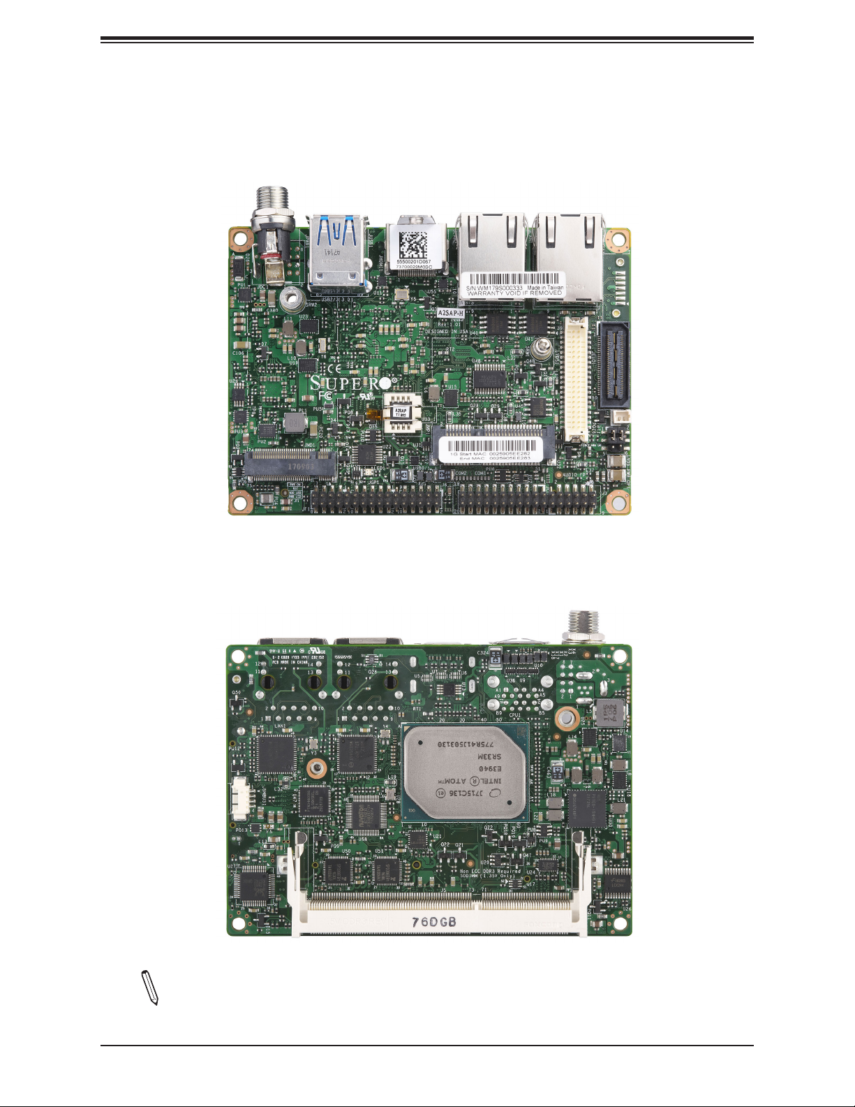
Figure 1-1. A2SAP-H Motherboard Image
Motherboard Bottom side
Chapter 1: Introduction
Motherboard TopSide
Note: All graphics shown in this manual were based upon the latest PCB revision
available at the time of publication of the manual. The motherboard you received may
or may not look exactly the same as the graphics shown in this manual.
9
Page 10
A2SAP-H/-E/-L User's Manual
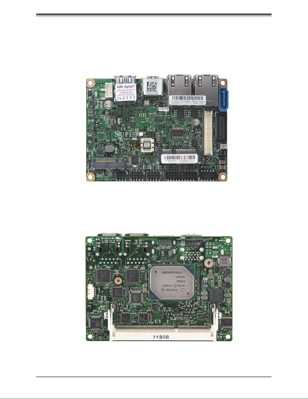
Figure 1-2. A2SAP-E/-L Motherboard Image
Motherboard Bottom side
Motherboard Topside
10
Page 11
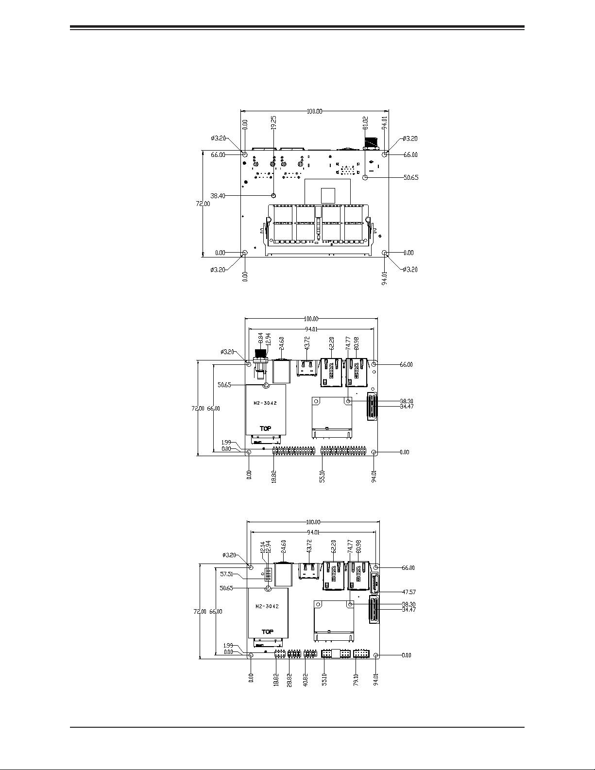
Figure 1-3. Motherboard Mechanical Drawings
A2SAP-H/-E/-L Motherboard Topside
Chapter 1: Introduction
A2SAP-H Motherboard Bottom Side
A2SAP-E/-L Motherboard Bottom Side
11
Page 12
A2SAP-H/-E/-L User's Manual
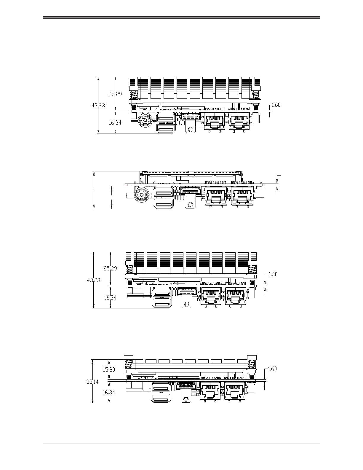
Figure 1-4. A2SAP-H/-E/-L Back Panel Mechanical Drawings
A2SAP-H Back Panel I/O with Heatsink
A2SAP-H Back Panel I/O without Heatsink
1.60
27.04
16.34
A2SAP-E Back Panel I/O with Heatsink
A2SAP-L Back Panel I/O with Heatsink
12
Page 13
Chapter 1: Introduction
JDC
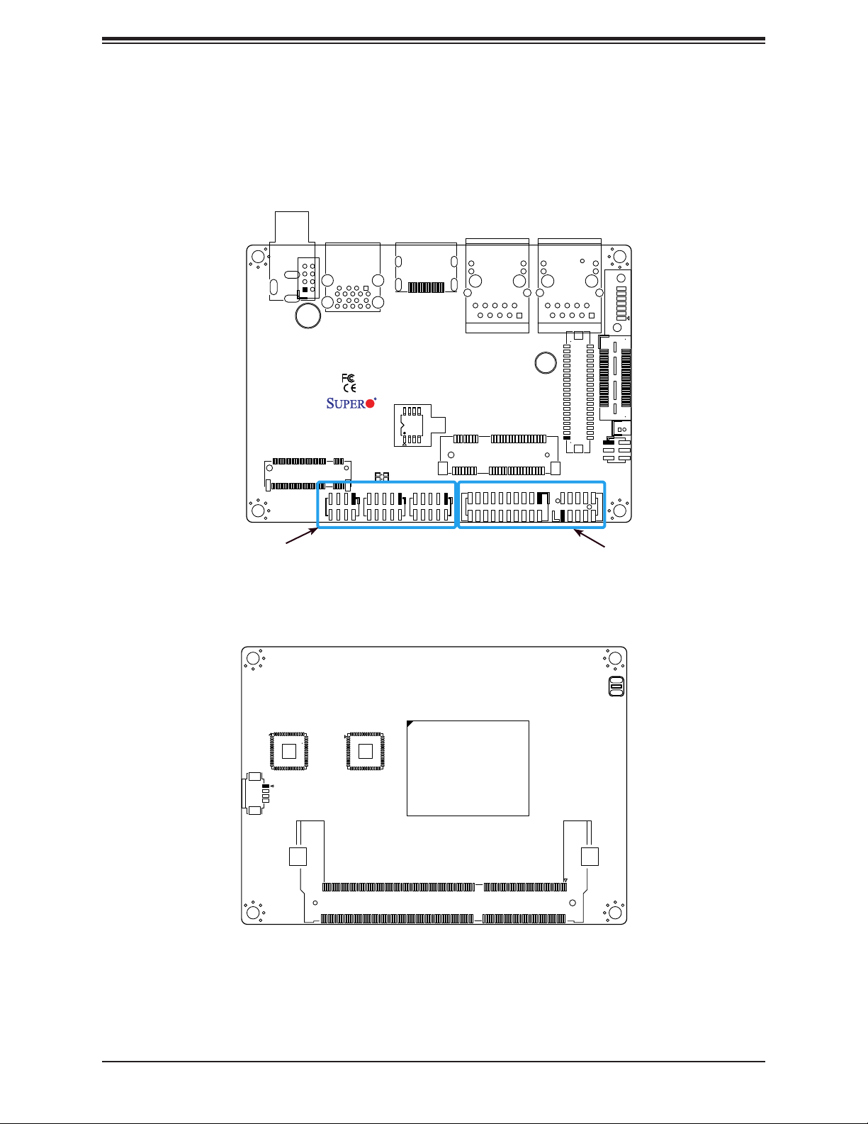
Figure 1-5. Motherboard Layout
(not drawn to scale)
A2SAP-H/-E/-L Bottom Layout
JPWR1
JHDMI1
JUSB1
USB2/3 (3.0)
SRW2
JMD1
JF1
JGP1
LED1
A2SAP-L
Rev:1.01
DESIGNED IN USA
J6: USB0/1
JLAN2
JMP1
JCOM1: COM1/COM2
SRW1
JLAN1
J3: AUDIO FP
LVDS1
JEIO1
BT1
JLCDPWR1
I-SATA1
1
32-Pin Connector A
(JF1 + JGP1 + J6)
(A2SAP-H only)
A2SAP-H/-E/-L Topside Layout
JSMBUS1
34-Pin Connector B
(JCOM1 + J3)
(A2SAP-H only)
PEC1
CPU1
J5
13
Page 14
A2SAP-H/-E/-L User's Manual
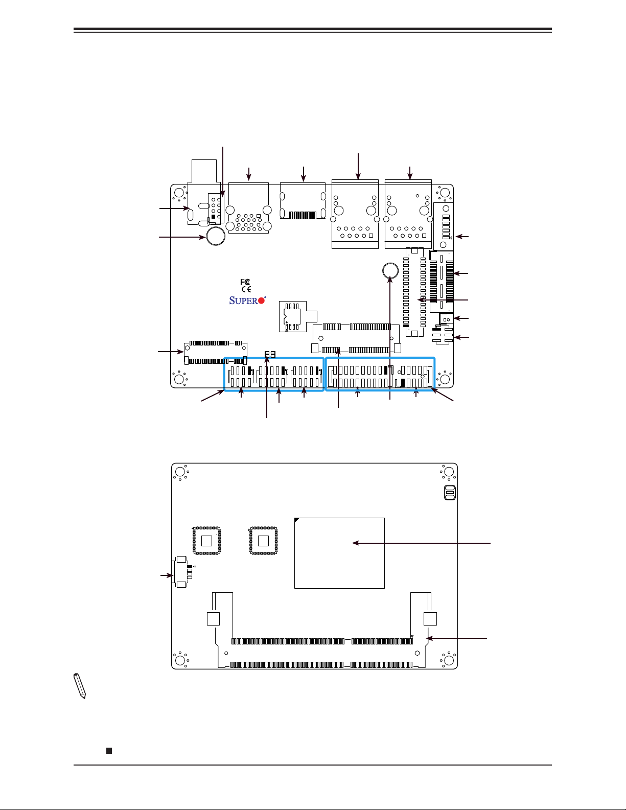
Quick Reference
Bottom Layout
JDC
SRW2
JMD1
32-Pin Connector A
(JF1 + JGP1 + J6)
(A2SAP-H only)
JDC
JPWR1
JPWR1
SRW2
JMD1
JF1
JUSB1
JUSB1
USB2/3 (3.0)
JF1
JGP1
LED1
LED1
JGP1
JHDMI1
JHDMI1
A2SAP-L
Rev:1.01
DESIGNED IN USA
J6: USB0/1
J6
JLAN2
JLAN2
JMP1
JCOM1: COM1/COM2
JCOM1
JMP1
SRW1
JLAN1
SRW1
JLAN1
LVDS1
J3: AUDIO FP
J3
I-SATA1
I-SATA1
JEIO1
JEIO1
LVDS1
BT1
BT1
1
JLCDPWR1
JLCDPWR1
34-Pin Connector B
(JCOM1 + J3)
(A2SAP-H only)
Topside Layout
PEC1
CPU1
CPU
JSMBUS1
JSMBUS1
J5
SODIMM
Notes:
• See Chapter 2 for detailed information on jumpers, I/O ports, and JF1 front panel connec-
tions. Jumpers and LED indicators not indicated are used for testing only.
• " " indicates the location of Pin 1.
14
Page 15

Chapter 1: Introduction
Quick Reference Table
Jumper Description Jumper Setting (Default *)
FORCE POWER ON
JLCDPWR1
LVDS Panel Power Source Selection
LED Description Status
LED1 Power LED
Connector Description
Battery Connector
BT1
I-SATA1 Intel® PCH SATA 3.0 Port
J3 Front Panel Audio Header (Mic-In/Headphone-out)
J6 Two USB 2.0 Headers
JCOM1 Two COM Headers (two RS232/422/485)
JDC 12V DC Jack Power Connector (for A2SAP-H)
JEIO1
JF1 Front Control Panel Header (Power/HDD LED, Reset, Power button)
JGP1 8-bit General Purpose I/O Header
JHDMI1 High Denition Multimedia Interface (HDMI) Port
JLAN1/JLAN2 LAN1/LAN2 (RJ45 LAN) Ports
JMD1 M.2 Slot (B-KEY 2242/3042) (SATA 3.0 / PCI-E x1 Gen2 / one USB 2.0)
JMP1 Half-Size Mini PCI-E Slot (supports PCI-E x1 Gen2 / one USB 2.0)
(To Clear CMOS, remove the battery, short pins 1-2 for more than 10 seconds and
install the battery.)
Supermicro Extension I/O
(DP/HDMI, two PCI-E x1, two USB 2.0, LPC, SATA, SMBus, SMBus,12Vsb 2A, 5Vsb
2.8A)
Notes: A2SAP-E/-L does NOT support SATA signal. The DP signal is supported
through a requested BIOS update.
Pins 2-4* (FORCE POWER ON)
Pins 4-6 (POWER BUTTON ON)
Pins 1-3* (3.3V)
Pins 3-5 (5V)
Solid Green: S0 mode
Solid Red: S3/S4/S5 modes
JPWR1 One 2x4-Pin 12V Power Connector (For A2SAP-E/L)
JSMBUS1 SMBus and 5V/1A SATA Power Box Header
JUSB1 Two Back Panel USB 3.0 Ports
LVDS1 Dual Channel 48-bit LVDS Connector
SRW1 - SRW2 M.2 and Mini PCI-E Mounting Holes
32-Pin Connector A Front panel, 8-bit GPIO and USB 2.0 x 2 (JF1 + JGP1 + J6) (A2SAP-H only)
34-Pin Connector B RS232/422/485 x 2 and Audio (JCOM1 + J3) (A2SAP-H only)
Note: Components not documented are for internal testing only.
15
Page 16
A2SAP-H/-E/-L User's Manual
Motherboard Features
Motherboard Features
CPU
• A2SAP-H/-E: Intel® Atom™ x5-E3940 Processor, Quad Core, 2 MB L2 Cache, 1.6GHz-1.8GHz, 9.5W
• A2SAP-L: Intel® Atom™ x5-E3930 Processor, Dual Core, 2 MB L2 Cache, 1.3GHz-1.8GHz, 6.5W
Memory
• Integrated memory controller supports up to 8GB of DDR3L 1333/1600/1866MHz Non-ECC 204-pin SO-DIMM
DIMM Size
• Single channel Non-ECC SO-DIMM, DDR3L 1333/1600/1866MHz up to 8GB
Expansion Slots
• One (1) Half-Size Mini PCI-E Slot (supports PCI-E x1 Gen2 / one USB 2.0)
• One (1) M.2 Slot (B-KEY 2242/3042) (SATA 3.0 / PCI-E x1 Gen2 / USB 2.0)
Network
• Dual Intel I210 controller
Graphics
• Features: OpenGL 5.0, DirectX 12, OpenCL 2.1
• Hardware Decode: AVC/H.264, MPEG2, VC1/WMV9, JPEG/MJPEG,
• Intel® HD Graphics GT Series
HEVC/H.265, VP8, VP9, MVC
• Hardware Encode: AVC/H.264, JPEG/MJPEG, HEVC/H.265, VP8, VP9, MVC
• Display: HDMI 1.4 (resolution up to 3840x2160 at 30Hz), LVDS (dual channel
48-bit, resolution up to 1920x1200 at 60Hz)
I/O Devices
• COM Header • Two (2) front accessible ports (JCOM1 supports two RS232/RS422/RS485)
• SATA Port • One (1) SATA 3.0 port (I-SATA1)
• Audio Port
• One (1) HD Audio header with Mic-in/Headphone-out (Realtek ALC888S) (Audio
on A2SAP-H/-E/-L only supports 0-60ºC)
• SMBus Header • One (1) SMBus box header
• One (1) Supermicro EI/O Header (DP/HDMI, two PCI-E x1, two USB 2.0, LPC,
• SMCI EI/O
SATA, SMBus, SMBus,12Vsb 2A, 5Vsb 2.8A)
Notes: A2SAP-E/-L does NOT support SATA signal. The DP signal is supported
through a requested BIOS update.
Peripheral Devices
• One (1) USB 3.0 port on the rear I/O panel (JUSB1)
• One (1) USB 2.0 header (J6)
BIOS
• 128Mb SPI AMI BIOS
®
• ACPI 3.0, SMBIOS 2.7, PCI F/W 3.0, BIOS rescue hot-key, RTC (Real Time Clock) wakeup
Note: The table above is continued on the next page.
16
Page 17

Chapter 1: Introduction
Motherboard Features
Power Management
• ACPI power management
• S3, S4, S5
• Power button override mechanism
• Power-on mode for AC power recovery
• Wake-On-LAN
• TXE Management Engine
• Force Power On by Jumper
• RTC Battery (typical voltage: 3.0V, normal discharge capacity: 220mAh)
System Health Monitoring
• Onboard voltage monitoring for +3.3V,+3.3V standby, VBAT, Vcore, system temperature, and memory voltage
• CPU switching phase voltage regulator
• CPU thermal trip support
System Management
• SuperDoctor® 5, Watch Dog, NMI, RoHs
LED Indicators
• Power/Suspend State Indicator LED
Dimensions
• 2.83" (L) x 3.93" (W) (72mm x 100mm) SBCs
• Height: A2SAP-H/-E 42.93mm, A2SAP-L 32.94mm
Environment
• Operating Temperature Range: A2SAP-H/-E support -30°C ~ 75°C (-22°F - 167°F), A2SAP-L supports -30°C ~ 60°C
(-22°F - 140°F). Note: The audio function operating temperature is 0~60°C.
• Non-Operating Temperature Range: -40°C - 85°C (-40°F - 185°F)
• Operating Relative Humidity Range: 8% - 90% (non-condensing)
• Non-Operating Relative Humidity Range: 10% - 95% (non-condensing)
Note 1: The CPU maximum thermal design power (TDP) is subject to chassis and
heatsink cooling restrictions. For proper thermal management, please check the chas-
sis and heatsink specications for proper CPU TDP sizing.
17
Page 18
A2SAP-H/-E/-L User's Manual
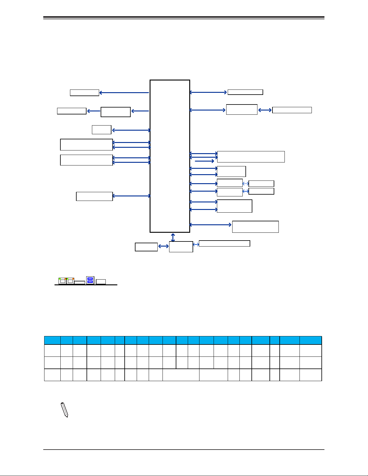
Figure 1-6.
System Block Diagram
HDMI connector
LVDS Connector
Rear USB3.0 connector (USB 0)
Rear USB3.0 connector (USB 1)
Rear USB3.0 connector (USB 2)
Rear USB3.0 connector (USB 3)
SMBUS_HEADER
I/O Panel Layout
USB 3.0
LAN1 LAN2
USB 3.0
HDMI
21
DP to LVDSBridge
FLASH
SPI 128Mb
DC_IN
PTN3460
DDI0
5.0Gb/s
5.0Gb/s
480Mb/s
480Mb/s
SMBUS
SPI
eDP
8-Bit GPIO
Intel
DDR3L non ECC SKU
FST_SPI
USB 2.0 [0]
USB 3.0 [0]
USB 2.0 [1]
USB 3.0 [1]
USB 2.0 [2]
USB 3.0 [3]
PCIE[4/5]
USB2.0 [4,5]
USB2.0[7]
PCIE[2]
PCIE[1]
PCIE[0]
SATA[1]
SATA[0]
LPC
NCT5523
Audio
SIO
SINGLE CHANNEL
DDR3L
1866/1600/1333 MHz
High Definition
PCIe Gen2 x 2
DDI1
PCIe Gen2 x 1
5.0GT/s
480Mb/s
PCIe Gen2 x 1
5.0GT/s
PCIe Gen2 x 1
5.0GT/s
PCIe Gen2 x 1
5.0GT/s
SATA
6Gb/s
COM 1 / 2 (RS232 / 422 / 485)
EIO (2 ports PCIe X1 / 2 ports USB 2.0 /
HDMI / LPC / SATA / SMBus)
Mini-PCIe Slot
GLAN2 (LAN2)
INTEL I210
GLAN2 (LAN1)
INTEL I210
M.2 SLOT (B KEY)
SATA 6Gb/s
MAX. 8G SO-DIMM SUPPORTED
Non-ECC-SODIMM0
REALTEK
ALC888S-VD2-GR
RJ45 (JLAN2)
RJ45 (JLAN1)
I-SATA0 (For A2SAP-E/-L)
JEIO1 (For A2SAP-H)
FRONT AUDIO Header
Figure 1-7.
A2SAP Series Specication Chart
Base
Turbo
Model CPU GbE HDMI LVDS
A2SAP-E E3940 2 Yes 21.8GHz1.66GHz 9.5W Yes 2 Yes 8-bit Yes 2 1 N/A Box header 1 -30°C ~ 75°C
A2SAP-L E3930 2 Yes 21.8GHz1.3GHz 6.5W Yes 2 Yes 8-bit Yes 2 1 N/A Box header 1 -30°C ~ 60°C
A2SAP-H E3940 2 Yes 21.8GHz1.66GHz 9.5W Yes 32-pin connector A 34-pin connector B N/A Yes DC Jack
Freq.
Freq.
CPU
TDP
USB3.0 USB2.0
Front
GPIO Audio COM SATA
Panel
EI/O
SATA
Power
conn
EI/O Temp.
1 -30°C~ 75°C
Note 1: Audio function operating temperature is 0~60°C only
Note 2: This is a general block diagram and may not exactly represent the features
on your motherboard. See the previous pages for the actual specications of your
motherboard.
18
Passive
Heatsink
25mm height
(SNK-C0115L)
15mm height
(SNK-C0116L)
25mm height
(SNK-C0115L)
Page 19

Chapter 1: Introduction
1.2 Processor Overview
Built upon the functionality and capability of the Intel® Atom SoC series processor, the
A2SAP-H/-E/-L motherboard offers maximum I/O expandability, energy efciency, and data
reliability in a 14-nm process architecture, and is optimized for embedded storage solutions,
networking applications, or cloud-computing platforms. The A2SAP-H/-E/-L drastically
increases system performance for a multitude of server applications.
The A2SAP-H/-E/-L supports the following features:
• Intel Virtualization Technology for Directed I/O (Intel VT-d)
• Enhanced Intel SpeedStep® Technology
• Video Connectors: HDMI and LVDS
• Adaptive Thermal Management/Monitoring
• Mini-PCI-E slot with PCI-E Gen2 X1 with transfer rates of up to 5Gb/s
• SATA port with SATA Gen3 with transfer rates of up to 6Gb/s
• System Management Bus (SMBus) Specication, Version 2.0
• M.2 slot with B-key 2242/3042 module
• Integrated Sensor Hub (ISH)
• Intel® Identity Protection Technology
1.3 Special Features
This section describes the health monitoring features of the A2SAP-H/-E/-L motherboard.
The motherboard has an onboard System Hardware Monitor chip that supports system health
monitoring.
19
Page 20

A2SAP-H/-E/-L User's Manual
Recovery from AC Power Loss
The Basic I/O System (BIOS) provides a setting that determines how the system will respond
when AC power is lost and then restored to the system. You can choose for the system to
remain powered off (in which case you must press the power switch to turn it back on), or
for it to automatically return to the power-on state. See the Advanced BIOS Setup section
for this setting. The default setting is Last State.
Note: Before setting the Recovery from AC Power Loss function in the BIOS, please
adjust force power on jumper JLCDPWR1 to pins 4-6 to disable the force power-on
function.
1.4 ACPI Features
ACPI stands for Advanced Conguration and Power Interface. The ACPI specication denes
a exible and abstract hardware interface that provides a standard way to integrate power
management features throughout a computer system including its hardware, operating system
and application software. This enables the system to automatically turn on and off peripherals
such as network cards, hard disk drives and printers.
In addition to enabling operating system-directed power management, ACPI also provides a
generic system event mechanism for Plug and Play and an operating system-independent
interface for conguration control. ACPI leverages the Plug and Play BIOS data structures
while providing a processor architecture-independent implementation that is compatible with
Windows® 10.
1.5 Power Supply
As with all computer products, a stable power source is necessary for proper and reliable
operation. It is even more important for processors that have high CPU clock rates. In areas
where noisy power transmission is present, you may choose to install a line lter to shield
the computer from noise. It is recommended that you also install a power surge protector to
help avoid problems caused by power surges.
20
Page 21

Chapter 1: Introduction
1.6 Super I/O
The Super I/O (NCT5523 chip) provides two high-speed, 16550 compatible serial
communication ports (UARTs), one of which supports serial infrared communication. Each
UART includes a 16-byte send/receive FIFO, a programmable baud rate generator, complete
modem control capability and a processor interrupt system. Both UARTs provide legacy speed
with baud rate of up to 115.2 Kbps as well as an advanced speed with baud rates of 250 K,
500 K, or 1 Mb/s, which support higher speed modems.
The Super I/O provides functions that comply with ACPI (Advanced Conguration and Power
Interface), which includes support of legacy and ACPI power management through a SMI
or SCI function pin. It also features auto power management to reduce power consumption.
The IRQs, DMAs and I/O space resources of the Super I/O can be exibly adjusted to meet
ISA PnP requirements, which support ACPI and APM (Advanced Power Management).
1.7 Advanced Power Management
The following new advanced power management features are supported by the motherboard.
Management Engine (ME)
Intel Atom SoC only supports the TXE function, also called CSE (Converged Security Engine),
which is the lite ME function.
21
Page 22

A2SAP-H/-E/-L User's Manual
Chapter 2
Installation
2.1 Static-Sensitive Devices
Electrostatic Discharge (ESD) can damage electronic com ponents. To prevent damage to your
motherboard, it is important to handle it very carefully. The following measures are generally
sufcient to protect your equipment from ESD.
Precautions
• Use a grounded wrist strap designed to prevent static discharge.
• Touch a grounded metal object before removing the board from the antistatic bag.
• Handle the board by its edges only; do not touch its components, peripheral chips, memory
modules or gold contacts.
• When handling chips or modules, avoid touching their pins.
• Put the motherboard and peripherals back into their antistatic bags when not in use.
• For grounding purposes, make sure that your chassis provides excellent conductivity be-
tween the power supply, the case, the mounting fasteners and the motherboard.
• Use only the correct type of CMOS onboard battery as specied by the manufacturer.
Unpacking
The motherboard is shipped in antistatic packaging to avoid static damage. When unpacking
the motherboard, make sure that the person handling it is static protected.
22
Page 23
Chapter 2: Installation
2.2 Motherboard Installation
All motherboards have standard mounting holes to t different types of chassis. Make sure
that the locations of all the mounting holes for both the motherboard and the chassis match.
Although a chassis may have both plastic and metal mounting fasteners, metal ones are
highly recommended because they ground the motherboard to the chassis. Make sure that
the metal standoffs click in or are screwed in tightly.
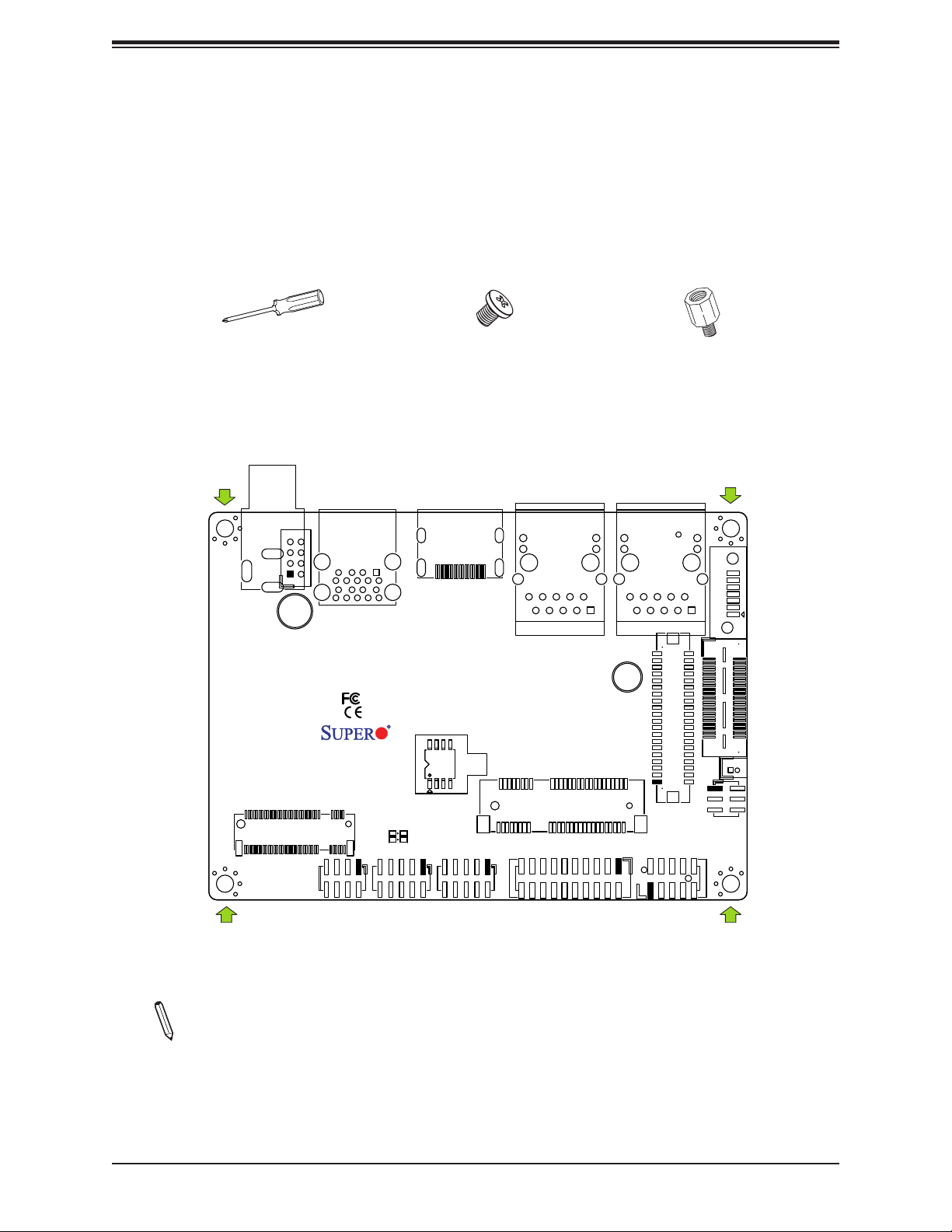
Phillips Screwdriver (1)
Tools Needed
JPWR1
JDC
SRW2
JMD1
JF1
JUSB1
USB2/3 (3.0)
Phillips Screws (4)
JHDMI1
Rev:1.01
DESIGNED IN USA
LED1
JGP1
J6: USB0/1
JLAN2
SRW1
JMP1
JCOM1: COM1/COM2
Standoffs (4)
Only if Needed
JLAN1
JEIO1
LVDS1
BT1
JLCDPWR1
J3: AUDIO FP
I-SATA1
1
Location of Mounting Holes
Note: 1) To avoid damaging the motherboard and its components, please do not use
a force greater than 8 lb/inch on each mounting screw during motherboard installation.
2) Some components are very close to the mounting holes. Please take precautionary
measures to avoid damaging these components when installing the motherboard to
the chassis.
23
Page 24
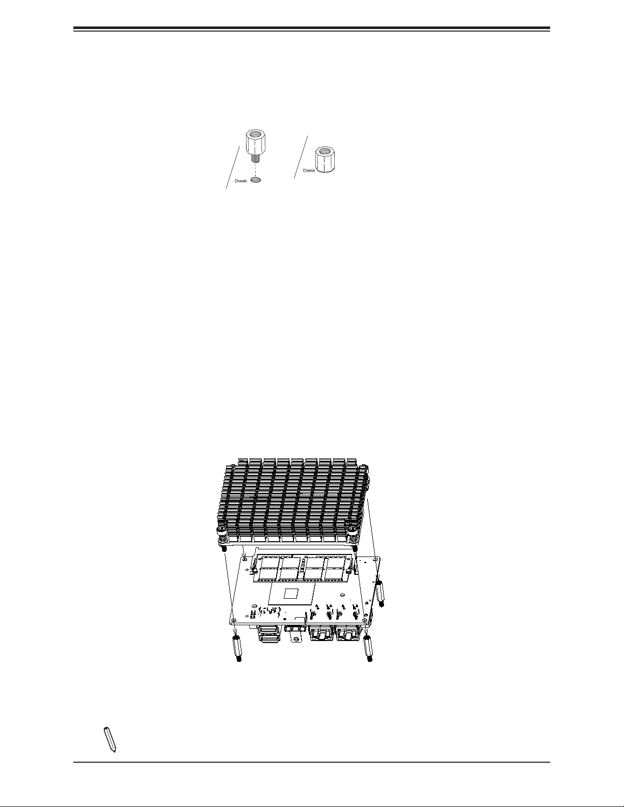
A2SAP-H/-E/-L User's Manual
Installing the Motherboard
1. Locate the mounting holes on the motherboard. See the previous page for the location.
2. Install standoffs in the chassis.
3. Install the memory. Follow section 2.3 - Memory Support and Installation
4. After the memory installation is complete, install the heatsink.
5. The thermal solution kit that comes with the motherboard includes one heatsink with
thermal grease and four copper standoffs that are 19mm in height. The copper standoff
type is determined by the customer's chassis design. The copper standoffs that are
19mm in height are recommended only.
6. To install the heatsink, remove the plastic cover on the bottom of the heatsink to expose
the thermal grease. Then place the heatsink directly on the CPU and make sure the
thermal grease is in contact with the CPU.
7. Turn the motherboard over and tighten the standoffs on the chassis with the
corresponding screws by using the Phillips screwdriver. Install the motherboard into the
chassis carefully to avoid damaging other motherboard components.
8. Make sure that the motherboard is securely placed in the chassis.
Note: Images displayed are for illustration only. Your chassis or components might
look different from those shown in this manual.
24
Page 25
Chapter 2: Installation
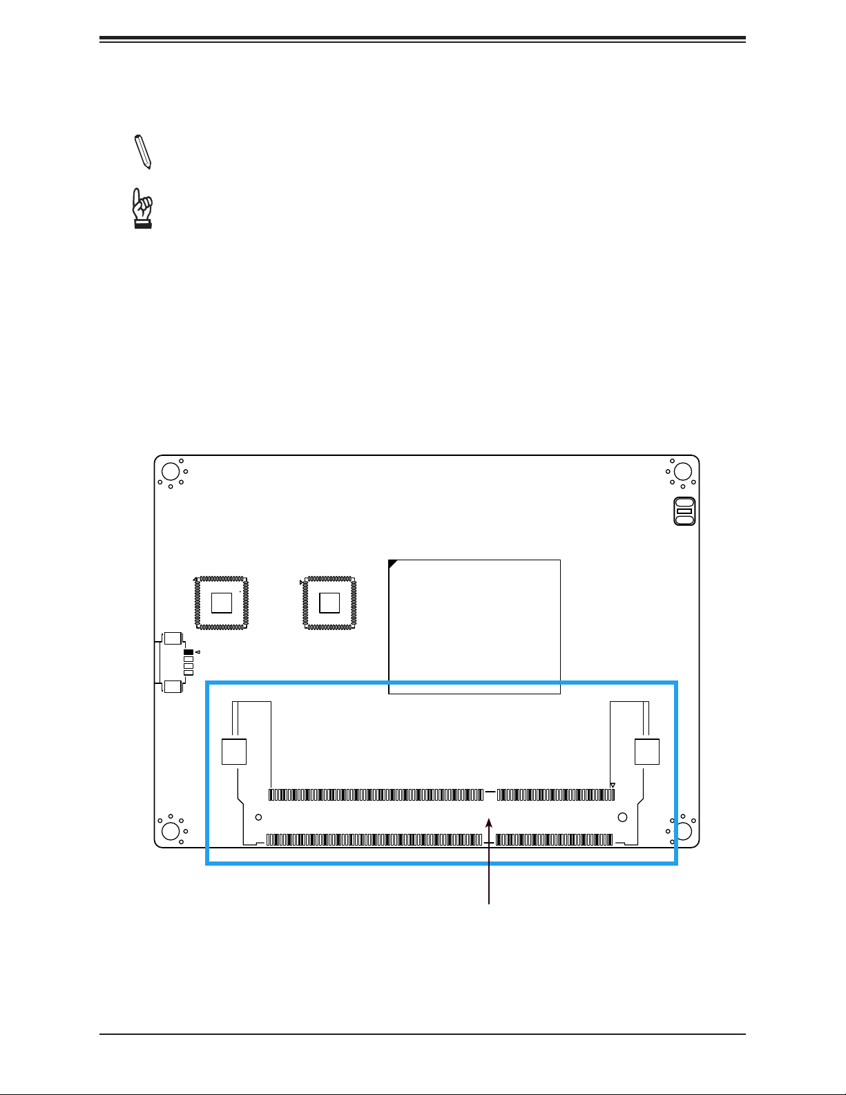
2.3 Memory Support and Installation
Note: Check the Supermicro website for recommended memory modules.
Important: Exercise extreme care when installing or removing DIMM modules to pre-
vent any possible damage.
Memory Support
The A2SAP-H/-E/-L supports up to 8GB of DDR3L Non-ECC SO-DIMM with speeds of
1333/1600/1866MHz in one memory slot on the bottom side of the motherboard.
Bottom Layout
JSMBUS1
PEC1
CPU1
J5
SO-DIMM Socket
25
Page 26
A2SAP-H/-E/-L User's Manual
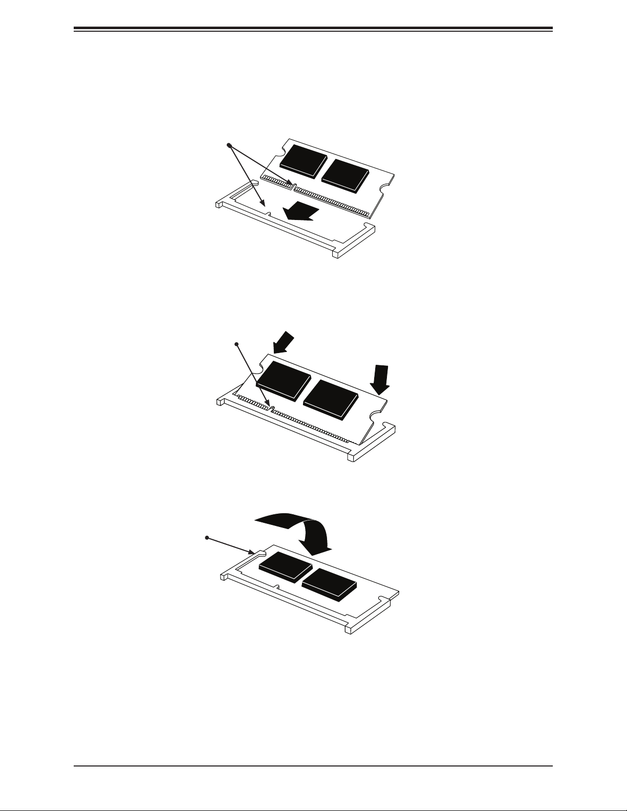
SO-DIMM Installation
1. Position the SO-DIMM module's bottom key so it aligns with the receptive point on the
slot.
Align
2. Insert the SO-DIMM module vertically at about a 45 degree angle. Press down until the
module locks into place.
Insert this end rst Press down until the module
locks into place.
3. The side clips will automatically secure the SO-DIMM module, locking it into place.
Locking clip
SO-DIMM Removal
1. Push the side clips at the end of the slot to release the SO-DIMM module. Pull the SODIMM module up to remove it from the slot.
26
Page 27
Chapter 2: Installation
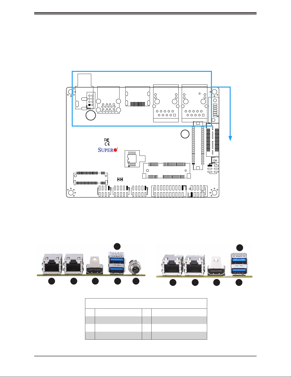
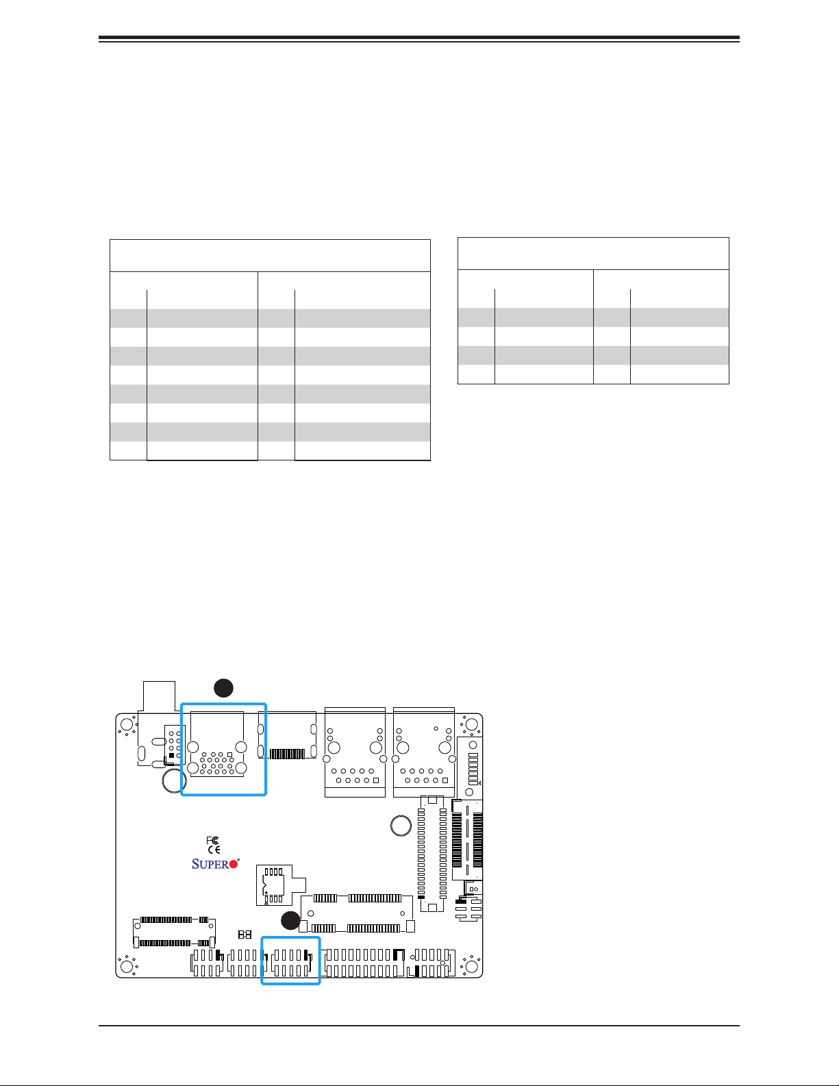
2.4 Rear I/O Ports
See Figure 2-1 below for the locations and descriptions of the various I/O ports on the rear
of the motherboard.
JPWR1
LED1
JHDMI1
Rev:1.01
DESIGNED IN USA
J6: USB0/1
JLAN2
SRW1
JMP1
JCOM1: COM1/COM2
JLAN1
JEIO1
LVDS1
BT1
JLCDPWR1
J3: AUDIO FP
JDC
SRW2
JMD1
JF1
JUSB1
USB2/3 (3.0)
JGP1
Figure 2-1. I/O Port Locations and Denitions
A2SAP-H A2SAP-E/-L
I-SATA1
1
4
1
6532
1 532
4
Rear I/O Ports
# Description # Description
1. LAN1 4. USB2
2. LAN2 5. USB1
3. HDMI 6. JDC
27
Page 28
A2SAP-H/-E/-L User's Manual
LAN Ports
Two LAN ports (JLAN1 - JLAN2) are located on the I/O back panel. These ports accept RJ45
type cables. Please refer to the LED Indicator section for LAN LED information. Refer to the
table below for pin dentions.
LAN Port
Pin Denition
Pin# Denition Pin# Denition
1 GND 9 TRD1+
2 CT_VCC 10 TRD1-
3 TRD4+ 11 GRN+/ORG-
4 TRD4- 12 GRN-/ORG+
5 TRD3+ 13 YEL+
6 TRD3- 14 YEL-
7 TRD2+ 15 SH1
8 TRD2- 16 SH2
HDMI Port
The HDMI (High-Denition Multimedia Interface) port is used to display both high denition
video and digital sound through an HDMI-capable display, using the same cable.
3
2
1
1. JLAN1
JPWR1
2. JLAN2
3. HDMI
LED1
JHDMI1
Rev:1.01
DESIGNED IN USA
J6: USB0/1
JLAN2
SRW1
JMP1
JCOM1: COM1/COM2
JLAN1
J3: AUDIO FP
LVDS1
JEIO1
BT1
JLCDPWR1
I-SATA1
1
JDC
SRW2
JMD1
JF1
JUSB1
USB2/3 (3.0)
JGP1
28
Page 29
Chapter 2: Installation
Universal Serial Bus (USB) Ports
There are two USB 3.0 ports (JUSB1) on the I/O back panel. The motherboard has two
additional USB 2.0 connections via the JEIO1 header. J6 also provides two front panel USB
2.0 connections. The onboard headers can be used to provide front side USB access with a
cable. Two USB 2.0 cables for front panel support are included with the motherboard single
retail package.
Back Panel USB 3.0
Pin Denition
Pin# Denition Pin# Denition
A1 VBUS B1 VBUS
A2 D1-N B2 D2-N
A3 D1-P B3 D2-P
A4 GND B4 GND
A5 Stda_SSRX1-N B5 Stda_SSRX2-N
A6 Stda_SSRX1-P B6 Stda_SSRX2-P
A7 GND_DRAIN B7 GND_DRAIN
A8 Stda_SSTX1-N B8 Stda_SSTX2-N
A9 Stda_SSTX1-P B9 Stda_SSTX2-P
Front Panel USB 2.0 Header
Pin Denition
Pin# Denition Pin# Denition
1 P5V_DUAL_F 2 P5V_DUAL_F
3 USBCON_N0 4 USBCON_N1
5 USBCON_P0 6 USBCON_P1
7 GND 8 GND
9 N/A 10 N/A
JDC
JPWR1
SRW2
JMD1
JF1
1
JUSB1
USB2/3 (3.0)
JGP1
LED1
JHDMI1
Rev:1.01
DESIGNED IN USA
2
J6: USB0/1
JLAN2
SRW1
JMP1
JCOM1: COM1/COM2
JLAN1
J3: AUDIO FP
29
LVDS1
JEIO1
BT1
JLCDPWR1
1. JUSB1
2. J6
I-SATA1
1
Page 30

A2SAP-H/-E/-L User's Manual
2.5 Front Control Panel
JF1 contains header pins for various buttons and indicators that are normally located on a
control panel at the front of the chassis. These connectors are designed specically for use
with Supermicro chassis. Refer to the gure below for the descriptions of the front control
panel buttons and LED indicators.
JPWR1
JDC
SRW2
JMD1
JF1
JHDMI1
JUSB1
USB2/3 (3.0)
Rev:1.01
DESIGNED IN USA
LED1
JGP1
J6: USB0/1
JCOM1: COM1/COM2
Figure 2-2. JF1 Header Pins
JLAN2
JMP1
SRW1
JLAN1
J3: AUDIO FP
LVDS1
JEIO1
BT1
JLCDPWR1
I-SATA1
1
PWR
Reset
Power Button
Reset Button
3.3V
3.3V Stby
1
78
30
2
Ground
Ground
HDD LED
Power LED
Page 31

Chapter 2: Installation
Power Button
The Power Button connection is located on pins 1 and 2 of JF1. Momentarily contacting both
pins will power on/off the system. This button can also be congured to function as a suspend
button (with a setting in the BIOS - see Chapter 4). To turn off the power in the suspend
mode, press the button for at least 4 seconds. Refer to the table below for pin denitions.
Power Button
Pin Denition (JF1)
Pin# Denition
1 Power Button
2 GND
Reset Button
The Reset Button connection is located on pins 3 and 4 of JF1. Attach it to a hardware reset
switch on the computer case to reset the system. Refer to the table below for pin denitions.
1
2
PWR
Reset
Power Button
Reset Button
3.3V
3.3V Stby
Reset Button
Pin Denition (JF1)
Pin# Denition
3 Reset
4 Ground
2
1
Ground
Ground
HDD LED
Power LED
1. Power Button
2. Reset Button
78
31
Page 32

A2SAP-H/-E/-L User's Manual
HDD LED
The HDD LED connection is located on pins 5 and 6 of JF1. Attach a cable here to indicate
the status of HDD-related activities, including SATA activities. Refer to the table below for
pin denitions.
HDD LED
Pin Denition (JF1)
Pin# Denition
5 +3.3V
6 HDD Active LOW
Power LED
The Power LED connection is located on pins 7 and 8 of JF1. Refer to the table below for
pin denitions.
PWR
Reset
Power Button
Reset Button
Power LED
Pin Denition (JF1)
Pin# Denition
7 +3.3VSB
8 Power LED LOW
2
1
Ground
Ground
1. HDD LED
2. Power LED
3.3V
3.3V Stby
78
HDD LED
Power LED
32
1
2
Page 33

Chapter 2: Installation
2.6 Connectors
Power Connections
12V DC Power Connector
JPWR1 is only available on the A2SAP-E/-L. It is a 2x4-pin, 2.0mm pitch box header, 12V
DC power source for the motherboard. The cable package includes a 2x4-pin to 2x2-pin
power cable.
12V DC Power
Pin Denition
Pin# Denition
1-4 P12VSB
5-8 GND
JDC
JDC, only available on the A2SAP-H, is a lockable DC jack power connector.
12V Stdby Power
Pin Denition
Pin# Denition
1 P12VSB
2 GND
3 GND
2
JPWR1
1
1. 12V DC Power
(JPWR1: 2x4 pin box
JDC
SRW2
JUSB1
USB2/3 (3.0)
JHDMI1
Rev:1.01
DESIGNED IN USA
JLAN2
JLAN1
SRW1
JEIO1
LVDS1
header)
I-SATA1
2. 12V DC Jack (JDC:
DC Jack)
JMD1
JF1
JGP1
LED1
J6: USB0/1
JMP1
JCOM1: COM1/COM2
33
JLCDPWR1
J3: AUDIO FP
BT1
1
Page 34

A2SAP-H/-E/-L User's Manual
Headers and Connectors
Front Panel Audio Header
A 10-pin front panel audio header located on the motherboard allows you to use the onboard
sound for audio playback. Connect an audio cable to the this header to use this feature. Refer
to the table below for pin denitions.
Audio Header
Pin Denition
Pin# Denition Pin# Denition
1 MIC_Left 2 AUDIO_GND
3 MIC_Right 4 AUDIO_Detect
5 LINE2_Right 6 MIC2_JD
7 Front AUDIO_JD 8 NC
9 LINE2_Left 10 LINE2_JD
Battery Connector
BT1 is a two-pin connector for an external CMOS battery. Refer to Chapter 3 for battery
installation instructions. This connector is also used to clear the CMOS. To clear the CMOS,
remove the battery, short pins 1-2 for more than 10 seconds and then install the battery.
JPWR1
1. Audio Header
2. Battery connector
JDC
SRW2
JUSB1
USB2/3 (3.0)
JHDMI1
Rev:1.01
DESIGNED IN USA
JLAN2
I-SATA1
JLAN1
SRW1
JEIO1
LVDS1
JMD1
JF1
JGP1
LED1
J6: USB0/1
JMP1
JCOM1: COM1/COM2
34
1
JLCDPWR1
J3: AUDIO FP
BT1
2
1
Page 35

Chapter 2: Installation
COM Headers
The JCOM1 header provides two RS232/422/485 COM connections. Refer to the table below
for pin denitions. Refer to pins 1 -10 for COM1 and pins 11 - 20 for COM2.
Serial COM Ports
Pin Denition
Pin# Denition Pin# Denition
DCD
1
or RS-485/422_COM1_TX- (Full Duplex)
or RS-485_COM1_Data- (Half Duplex)
RXD
3
or RS-485/422_COM1_TX+ (Full Duplex)
or RS-485_COM1_Data+ (Half Duplex)
5 TXD or RS-485/422_COM1_RX+ (Full Duplex) 6 CTS
7 DTR or RS-485/422_COM1_RX- (Full Duplex) 8 RI_N
9 GND 10 N/A
DCD
11
or RS-485/422_COM2_TX- (Full Duplex)
or RS-485_COM2_Data- (Half Duplex)
RXD
13
or RS-485/422_COM2_TX+ (Full Duplex)
or RS-485_COM2_Data+ (Half Duplex)
15 TXD or RS-485/422_COM2_RX+ (Full Duplex) 16 CTS
17 DTR or RS-485/422_COM2_RX- (Full Duplex) 18 RI_N
19 GND 20 N/A
DSR
2
RTS
4
DSR
12
RTS
14
SATA Ports
The A2SAP-E/-L has one SATA 3.0 port (I-SATA1) that is supported by the Intel® Atom SoC.
A2SAP-H doesn't have a SATA port (I-SATA1). The A2SAP-H SATA signal passes through
the EI/O (JEIO) connector.
JPWR1
2
1. JCOM1
2. I-SATA1
JGP1
LED1
JHDMI1
Rev:1.01
DESIGNED IN USA
J6: USB0/1
JLAN2
SRW1
JMP1
1
JCOM1: COM1/COM2
JLAN1
LVDS1
J3: AUDIO FP
JEIO1
BT1
JLCDPWR1
I-SATA1
1
JDC
SRW2
JMD1
JF1
JUSB1
USB2/3 (3.0)
35
Page 36

A2SAP-H/-E/-L User's Manual
LVDS Connector
LVDS1 is the LVDS connector. LVDS (low-voltage differential signaling) is a high-speed
digital interface that operates at low power. It is a type of connection that is used with a
LVDS LCD panel. The connector combines LCD VCC Power (pins 9-10), LVDS high speed
digital interface, backlight power 3.3V (pin 7) and 12V (pins 1-5), backlight enable (pin 15),
and dimming control (pin 13). Select the correct LCD VCC power according to the LCD
specication by JLCDPWR1 (short pins 1-3 for 3.3V, short pins 3-5 for 5V) before enabling
the LVDS panel. Tho choose the LCD VCC power, short JLCDPWR1 pins 1-3 for 3.3V or
short pins 3-5 for 5V. Refer to the tables below for vendor part number, mating, and crimping
contact connector information before making the LVDS/backlight cable.
LVDS Connector
Connector Vendor Manufacture P/N Description
Onboard LVDS
Connector
HIROSE DF13E-40DP-1.25V(51)
Mating Connector HIROSE DF13-40DS-1.25C
BOX HEADER, BOARD TO WIRE, 2X20, PITCH 1.25MM,
VERT, 1A/PIN, WHITE, 0.2UM GOLD, PA9T, MATING
HEIGHT 5.8MM
Headers and Wire Housings 1.25MM RECEPT HSNG 40P
DUAL ROW CRIMP
Crimping Contact
Connector
JPWR1
JDC
USB2/3 (3.0)
SRW2
JMD1
JF1
HIROSE
1. LVDS Connector
JHDMI1
JUSB1
Rev:1.01
DESIGNED IN USA
LED1
JGP1
J6: USB0/1
DF13G-2630SCFA
JLAN2
JLAN1
SRW1
1
JMP1
JCOM1: COM1/COM2
LVDS1
J3: AUDIO FP
Headers and Wire Housings SOCKET CONTACT/REEL
AWG26-30
LVDS Connector
Pin Denitions
Pin# Denition Pin# Denition
39 GND 40 GND
37 LVDSB D3N 38 LVDSB D3P
35 LVDSB CLKN 36 LVDSB CLKP
33 LVDSB D2N 34 LVDSB D2P
31 LVDSB D1N 32 LVDSB D1P
29 LVDSB D0N 30 LVDSB D0P
27 GND 28 GND
25 LVDSA D3N 26 LVDSA D3P
23 LVDSA CLKN 24 LVDSA CLKP
I-SATA1
21 LVDSA D2N 22 LVDSA D2P
19 LVDSA D1N 20 LVDSA D1P
JEIO1
17 LVDSA D0N 18 LVDSA D0P
15 BKLTEN 16 GND
BT1
1
13 BKLTCTL 14 PVCCEN
11 DDC CLK 12 DDC DATA
JLCDPWR1
9 LCDVCC 10 LCDVCC
7 3.3V 8 GND
5 12V 6 GND
3 12V 4 12V
1 12V 2 12V
36
Page 37

Chapter 2: Installation
General Purpose I/O Header
The JGP1 (General Purpose Input/Output) header is an 8-bit general purpose I/O expander
on a pin header via the SMBus. Refer to the table below for pin denitions.
GPIO Header
Pin Denition
Pin# Denition Pin# Denition
1 P3V3SB 2 GND
3 GP_P3V3_GP0 4 GP_P3V3_GP4
5 GP_P3V3_GP1 6 GP_P3V3_GP5
7 GP_P3V3_GP2 8 GP_P3V3_GP6
9 GP_P3V3_GP3 10 GP_P3V3_GP7
M.2 Slot
M.2 is formerly known as Next Generation Form Factor (NGFF) and is located at JMD1 on
the motherboard. The M.2 slot is designed for internal mounting devices. The A2SAP-H/-E/-L
motherboard deploys a B-KEY for SATA/PCI-E SSD devices or USB/PCI-E WWAN or GNSS
card. The A2SAP-H/-E/-L deploys a 2242/3042 screw hole location for a 2242/3042 M.2
module.
JDC
JPWR1
SRW2
2
JMD1
JF1
JUSB1
USB2/3 (3.0)
1
JGP1
LED1
JHDMI1
Rev:1.01
DESIGNED IN USA
J6: USB0/1
JLAN2
SRW1
JMP1
JCOM1: COM1/COM2
37
JLAN1
J3: AUDIO FP
LVDS1
JEIO1
BT1
JLCDPWR1
1. General Purpose
Header
2. M.2 Slot
I-SATA1
1
Page 38

A2SAP-H/-E/-L User's Manual
JEIO1
This Supermicro EI/O header provides exibility support for the following functions: DP/HDMI,
PCIe x2, two USB 2.0, LPC, SATA, SMBus, and Power, so that it allows customers to make
their own I/O module to t different kinds of vertical market I/O demands.
The A2SAP-E/-L does NOT support
the SATA signal through the EI/O
header. The DP signal is supported
through a requested BIOS update.
Functions
SATA
PCI Express
USB
LPC
SMBus
DDI
Power
Misc
GND
1. Supermicro EI/O Header
JPWR1
JDC
SRW2
JMD1
JF1
JUSB1
USB2/3 (3.0)
JHDMI1
JLAN1
JLAN2
Rev:1.01
DESIGNED IN USA
LED1
JGP1
J6: USB0/1
SRW1
JMP1
JCOM1: COM1/COM2
1
LVDS1
J3: AUDIO FP
JEIO1
BT1
JLCDPWR1
1
Pin# Denition Pin# Denition
1 PCIE_EIO_RX_DP0 61
3 PCIE_EIO_RX_DN0 4 PCIE_EIO_TX_DN0
5 GND 6 GND
7 PCIE_EIO_RX_DP1 8 PCIE_EIO_TX_DP1
9 PCIE_EIO_RX_DN1 10 PCIE_EIO_TX_DN0
11 GND 12 GND
13 CLK_100M_EIO_DP 14 USB_P5_DP
15 CLK_100M_EIO_DN 16 USB_P5_DN
17 GND 62
19 DDI1_TXP2 20 USB_P4_DN
21 DDI1_TXN2 22 GND
23 GND 24 DDI1_TXP3
25 DDI1_TXP1 26 DDI1_TXN3
27 DDI1_TXN1 28 GND
29 GND 30 DDI_HPD
31 DDI1_TXP0 32 SOC_WAKE_EIO_N
33 DDI1_TXN0 63
35 GND 36 DDI1_DDC_P1V8_
37 DDI1_AUXP 38 SOC_SMB_CLK
39 DDI1_AUXN 40 SOC_SMB_DAT
41 P5VSB 42 P3VSB
43 P5VSB 44 LPC_LFRAME_N
45 P12VSB 46 LPC_AD3
47 SOC_LPC_CLKOUT1 64
I-SATA1
49 PLTR_
TPM_80PORT_N
51 LPC_SERIRQ 52 LPC_AD0
53 P3V3 54 P5V
55 PS_ON_N 56 GND
57 EIO_SATA_TXP0 58 EIO_SATA_RXN0
59 EIO_SATA_TXN0 60 EIO_SATA_RXP0
Supermicro EI/O
Pin Denition
2 PCIE_EIO_TX_DP0
GND
18 USB_P4_DP
GND
34 DDI1_DDC_P1V8_
GND
48 LPC_AD2
GND
50 LPC_AD1
DAT
CLK
38
Page 39

Chapter 2: Installation
JEIO1 (continued)
The table below shows the EI/O connector size, part numbers, and information for board-toboard stackable mating connector for a user’s I/O module.
EI/O Connector
Connector Size Manufacture P/N
EI/O Connector
on A2SAP
Mating connector on
I/O module
Mating connector on
I/O module
Mating connector on
I/O module
0.5mm pitch, 60pin Samtec P/N: QSH-030-01-L-D-A-K-TR)
0.5mm pitch, 60pin
11mm height
0.5mm pitch, 60pin
16mm height
0.5mm pitch, 60pin
19mm height
Samtec P/N: QTH-030-03-L-D-A-K-TR
Samtec P/N: QTH-030-04-L-D-A-K-TR
Samtec P/N: QTH-030-05-L-D-A-K-TR
Note: Contact the Supermicro Sales department to obtain the board's 3D drawing
to make your own EI/O I/O module. Make sure the I/O module can be mechanically
assembled on the A2SAP.
39
Page 40

A2SAP-H/-E/-L User's Manual
JDC
SRW2
JPWR1
JLAN2
JLAN1
USB2/3 (3.0)
JHDMI1
I-SATA1
JUSB1
32-Pin Connector A (JF1 + JGP1 + J6) (A2SAP-H only)
A2SAP-H combines JF1, JGP1 and J6 into a 32-pin, 2.0mm pitch pin header, including the
front panel (power/HDD LED, power/reset button), 8-bit GPIO, and two USB 2.0 connections.
Refer to the table below for pin denitions and the female mating connector information.
The distance between the board-to-board stack is 11mm in height while using the male pin
header (PINREX P/N:225-97-16GBEW) to stack onto the female mating connector (PINREX
P/N: 620-92-16GB00).
32-Pin Connector A
Connector Supermicro P/N Vendor Manufacture P/N Description
Male Pin Header
on A2SAP-H
Female Mating
Connector
Function Pin# Silkscreen Pin # Denition Pin# Silkscreen Pin # Denition
Two USB 2.0
(J6: USB0/1)
N/A 11 N/A N/A 12 N/A N/A
8-bit GPIO
(JGP1)
N/A 23 N/A N/A 24 N/A N/A
Front Panel
(JF1)
HDR-0208L-0000-
PRX
HDR-0210L-0000-
PRX
PINREX 225-97-16GBEW
PINREX
620-92-16GB00
CNT, PIN/HEADER, 2X16 PIN, PITCH 2MM,
VERT, 1A/PIN, BLACK, GF, NY6T, SMD, CM
(-30 ~ 75C), ROHS
CNT, PIN FEMALE HEADER, 2X16 PIN,
PITCH 2MM, VERT,1A/PIN, BLACK, GF,
TL2.3MM, NY6T, DIP, EX (-40 ~ 105C), ROHS
32-Pin Connector A
Pin Denitions
1 1 P5V_DUAL_F 2 2 P5V_DUAL_F
3 3 USBCON_N0 4 4 USBCON_N1
5 5 USBCON_P0 6 6 USBCON_P1
7 7 GND 8 8 GND
9 9 N/A 10 10 N/A
13 1 P3V3SB 14 2 GND
15 3 GPIO_1 16 4 GPIO_5
17 5 GPIO_2 18 6 GPIO_6
19 7 GPIO_3 20 8 GPIO_7
21 9 GPIO_4 22 10 GPIO_8
25 1 Power Button 26 2 GND
27 3 Reset Button 28 4 GND
29 5 3.3V 30 6 SATA HDD LED
31 7 3.3Vstby 32 8 PWR LED
Rev:1.01
JGP1
1
LED1
DESIGNED IN USA
J6: USB0/1
JMD1
JF1
SRW1
JMP1
JCOM1: COM1/COM2
JEIO1
1. 32-Pin Connector A
LVDS1
BT1
1
2
JLCDPWR1
J3: AUDIO FP
2. 34-Pin Connector B (on the next
page)
40
Page 41

Chapter 2: Installation
34-Pin Connector B (JCOM1 + J3) (A2SAP-H only)
A2SAP-H combines JCOM1 and J3 into a 34-pin, 2.0mm pitch pin header, including two RS232/422/485 connections and an audio (Mic-in/Headphone-out) connection. Refer to the table
below for pin denitions and the female mating connector information. The distance between
board-to-board stack is 11mm in height while using male pin header (PINREX P/N:225-9717GBEW) to stack onto female mating connector (PINREX P/N:620-92-17GB00).
34-Pin Connector B
Connector Supermicro P/N Vendor Manufacture P/N Description
Male Pin Header
on A2SAP-H
Female Mating
Connector on I/O
Module
HDR-0209L-0000-
PRX
HDR-0211L-0000-
PRX
PINREX 225-97-17GBEW
PINREX
620-92-17GB00
CNT, PIN/HEADER, 2X17 PIN, PITCH 2MM,
VERT, 1A/PIN, BLACK, GF, NY6T, SMD, CM
(-30 ~ 75C), ROHS
CNT, PIN FEMALE HEADER, 2X17 PIN,
PITCH 2MM, VERT, 1A/PIN, BLACK, GF,
TL2.3MM, NY6T, DIP, EX (-40 ~ 105C), ROHS
34-Pin Connector B
Pin Denitions
Function Pin# Silkscreen
AUDIO
(J3: Audio FP)
N/A 11 N/A N/A 12 N/A N/A
N/A 13 N/A N/A 14 N/A N/A
Two
RS-232/422/485
(JCOM1: COM1/
COM2)
Pin #
1 10 LINE2_JD 2 9 LINE2_Left
3 8 NC 4 7 Front AUDIO_JD
5 6 MIC2_JD 6 5 LINE2_Right
7 4 AUDIO_Detect 8 3 MIC_Right
9 2 AUDIO_GND 10 1 MIC_Left
15 1 DCD
17 3 RXD
19 5 TXD
21 7 DTR
23 9 GND 24 10 N/A
25 11 DCD
27 13 RXD
29 15 TXD
31 17 DTR
33 19 GND 34 20 N/A
Denition Pin# Silkscreen
Pin #
16 2 DSR
or RS-485/422_COM1_TX- (Full Duplex)
or RS-485_COM1_Data- (Half Duplex)
18 4 RTS
or RS-485/422_COM1_TX- (Full Duplex)
or RS-485_COM1_Data- (Half Duplex)
20 6 CTS
or RS-485/422_COM1_RX+ (Full
Duplex)
22 8 RI_N
or RS-485/422_COM1_RX- (Full Duplex)
26 12 DSR
or RS-485/422_COM2_TX- (Full Duplex)
or RS-485_COM2_Data- (Half Duplex)
28 14 RTS
or RS-485/422_COM2_TX+ (Full Duplex)
or RS-485_COM2_Data+ (Half Duplex)
30 16 CTS
or RS-485/422_COM2_RX+ (Full
Duplex)
32 18 RI_N
or RS-485/422_COM2_RX- (Full Duplex)
Denition
41
Page 42

A2SAP-H/-E/-L User's Manual
Mini PCI-E Slot
The Mini PCI-E slot, located at JMP1 on the bottom side of the motherboard, is used to install
a compatible Mini PCI-E device. The Mini PCI-E slot supports modules which are USB or
PCI-E x1 devices, such as wireless, GNSS, and Bluetooth modules. See the table below for
pin denitions.
Mini PCI-E
Pin Denition
Pin# Denition Pin# Denition
52 +3.3Vaux 51 NC
50 GND 49 NC
48 +1.5V 47 NC
46 NC 45 NC
44 NC 43 NC
42 NC 41 +3.3Vaux
40 GND 39 NC
38 USB_D+ 37 GND
JDC
JPWR1
SRW2
JMD1
JF1
1. Mini PCI-E
JUSB1
USB2/3 (3.0)
JGP1
LED1
JHDMI1
Rev:1.01
DESIGNED IN USA
J6: USB0/1
JLAN2
SRW1
1
JMP1
JCOM1: COM1/COM2
JLAN1
LVDS1
J3: AUDIO FP
JEIO1
BT1
JLCDPWR1
1
36 USB_D- 35 GND
34 GND 33 PETp0
32 SMB_DATA 31 PETn0
30 SMB_CLK 29 GND
28 +1.5V 27 GND
26 GND 25 PERp0
24 +3.3Vaux 23 PERn0
22 PERST# 21 DET_CARD_
20 NC 19 NC
I-SATA1
18 GND 17 NC
16 NC 15 GND
14 NC 13 REFCLK+
12 NC 11 REFCLK-
10 NC 9 GND
8 NC 7 CLKREQ#
6 1.5V 5 NC
4 GND 3 NC
2 3.3Vaux 1 WAKE#
PLUG
42
Page 43

Chapter 2: Installation
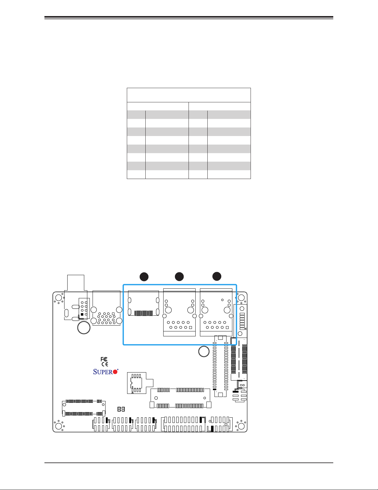
System Management Bus Header and SATA Power
A System Management Bus header for additional slave devices or sensors is located at
JSMBUS1 on the bottom side of the motherboard. This header also serves as a 5V/1A SATA
power box header. Refer to the table below for pin denitions.
Note: The SATA power cable is included in the retail and bulk packages. The
Supermicro part number is CBL-PWEX-1030.
SMBus Header
Pin Denition
Pin# Denition
1 SMB_CLK
2 SMB_DATA
3 GND
4 P5V
JSMBUS1
Bottom Layout
1. SMBus Header
PEC1
CPU1
1
J5
43
Page 44

A2SAP-H/-E/-L User's Manual
2.7 Jumper Settings
How Jumpers Work
To modify the operation of the motherboard, jumpers can be used to choose between optional
settings. Jumpers create shorts between two pins to change the function of the connector.
Pin 1 is identied with a square solder pad on the printed circuit board. See the diagram
below for an example of jumping pins 1 and 2. Refer to the motherboard layout page for
jumper locations.
Note: On two-pin jumpers, Closed means the jumper is on and Open means the
jumper is off the pins.
Connector
Pins
Jumper
Setting
3 2 1
3 2 1
44
Page 45

Chapter 2: Installation
JLCDPWR1
LVDS VCC Power Source Selection
Use this jumper to select the power voltage for the LVDS panel. Make sure that the
specications of the cable is compatible with the panel to prevent damage. See the table
below for jumper setting information.
Force power on
Use jumper JLCDPWR1 (Pins 2-4/4-6) to select the FORCE POWER ON function when the
AC power cord is plugged in. When enabling force power on and AC power recovery, the
system will boot up automatically without pressing the power button. See the table below for
jumper setting information.
LVDS VCC Power Source Selection
Jumper Settings
Jumper Setting Denition
Pins 1-3 3.3V (Default)
Pins 3-5 5V
JPWR1
JDC
SRW2
JUSB1
USB2/3 (3.0)
JHDMI1
Rev:1.01
DESIGNED IN USA
JLAN2
SRW1
JLAN1
LVDS1
Jumper Setting Denition
Pins 2-4
Pins 4-6
I-SATA1
JEIO1
FORCE POWER ON
Jumper Settings
FORCE POWER ON (Default)
(when the AC power cord is
plugged)
POWER BUTTON ON
(when the AC power cord is
plugged)
1. JLCDPWR1
JMD1
JMP1
BT1
1
1
LED1
JGP1
J6: USB0/1
JF1
JCOM1: COM1/COM2
JLCDPWR1
J3: AUDIO FP
45
Page 46

A2SAP-H/-E/-L User's Manual
2.8 LED Indicators
LAN Port LEDs
There are two LAN ports (JLAN1 and JLAN2) on the I/O back panel of the motherboard. Each
Ethernet LAN port has two LEDs. The green LED indicates activity, while the other Link LED
may be green, amber, or off to indicate the speed of the connection.
LAN1/2 LED
(Connection Speed
Indicator)
LED Color Denition
Off 10 Mb/s
Green 100 Mb/s
Amber 1 Gb/s
Power LED
LED1 is the Power LED. In S0 mode, this LED will be solid green. In S3/S4/S5 modes, this
LED will be solid red.
JDC
JPWR1
SRW2
JMD1
JF1
JUSB1
USB2/3 (3.0)
JGP1
3
LED1
Onboard Power LED Indicator
LED Color Denition
System Off
Off
(power cable not
connected)
Solid Green S0 mode
Solid Red S3/S4/S5 modes
2
JHDMI1
JLAN2
Rev:1.01
DESIGNED IN USA
JMP1
J6: USB0/1
JCOM1: COM1/COM2
SRW1
JLAN1
J3: AUDIO FP
1
LVDS1
JEIO1
BT1
JLCDPWR1
1. JLAN1 Port LED
2. JLAN2 Port LED
3. Power LED
I-SATA1
1
46
Page 47

Chapter 3: Troubleshooting
Chapter 3
Troubleshooting
3.1 Troubleshooting Procedures
Use the following procedures to troubleshoot your system. If you have followed all of the
procedures below and still need assistance, refer to the ‘Technical Support Procedures’ and/
or ‘Returning Merchandise for Service’ section(s) in this chapter. Always disconnect the AC
power cord before adding, changing or installing any non hot-swap hardware components.
Before Power On
1. Check that the power LED on the motherboard is on.
2. Make sure that the power connector is connected to your power supply.
3. Make sure that no short circuits exist between the motherboard and chassis.
4. Disconnect all cables from the motherboard, including those for the keyboard and
mouse.
5. Remove all add-on cards.
6. Install a heatsink and connect the power to the motherboard. Make sure that the
heatsink is fully seated. Check all jumper settings as well.
7. Use the correct type of CMOS battery (CR2032) as recommended by the manufacturer.
No Power
1. Make sure that no short circuits exist between the motherboard and the chassis.
2. Verify that all jumpers are set to their default positions.
3. Turn the power switch on and off to test the system.
4. The battery on your motherboard may be old. Check to verify that it still supplies
~3VDC. If it does not, replace it with a new one.
47
Page 48

A2SAP-H/-E/-L User's Manual
Memory Errors
1. Make sure that the DIMM modules are properly and fully installed.
2. Conrm that you are using the correct memory. Also, it is recommended that you use
the same memory type and speed for all DIMMs in the system. See Section 2.4 for
memory details.
3. Check for bad DIMM modules or slots by swapping modules between slots and noting
the results.
Losing the System's Setup Conguration
1. Make sure that you are using a high quality power supply. A poor quality power supply
may cause the system to lose the CMOS setup information. Refer to Section 1.5 for
details on recommended power supplies.
2. The battery on your motherboard may be old. Check to verify that it still supplies
~3VDC. If it does not, replace it with a new one.
3. If the above steps do not x the setup conguration problem, contact your vendor for
repairs.
When the System Becomes Unstable
A. If the system becomes unstable during or after OS installation, check the following:
1. Memory support: Make sure that the memory modules are supported by testing the
modules using memtest86 or a similar utility.
Note: Click on the Tested Memory List link on the motherboard product page to see
a list of supported memory.
2. HDD support: Make sure that all hard disk drives (HDDs) work properly. Replace the
bad HDDs with good ones.
3. Heatsink: Check that the heatsink is installed properly.
4. Adequate power supply: Make sure that the power supply provides adequate power to
the system. Make sure that all power connectors are connected. Please refer to our
website for more information on the minimum power requirements.
5. Proper software support: Make sure that the correct drivers are used.
48
Page 49

Chapter 3: Troubleshooting
B. If the system becomes unstable before or during OS installation, check the following:
1. Source of installation: Make sure that the devices used for installation are working
properly, including boot devices such as CD/DVD and CD/DVD-ROM.
2. Cable connection: Check to make sure that all cables are connected and working
properly.
3. Using the minimum conguration for troubleshooting: Remove all unnecessary
components (starting with add-on cards rst), and use the minimum conguration (but
with a CPU and a memory module installed) to identify the trouble areas. Refer to the
steps listed in Section A above for proper troubleshooting procedures.
4. Identifying bad components by isolating them: If necessary, remove a component in
question from the chassis, and test it in isolation to make sure that it works properly.
Replace a bad component with a good one.
5. Check and change one component at a time instead of changing several items at the
same time. This will help isolate and identify the problem.
6. To nd out if a component is good, swap this component with a new one to see if the
system will work properly. If so, then the old component is bad. You can also install the
component in question in another system. If the new system works, the component is
good and the old system has problems.
49
Page 50

A2SAP-H/-E/-L User's Manual
3.2 Technical Support Procedures
Before contacting Technical Support, please take the following steps. Also, note that as a
motherboard manufacturer, we do not sell directly to end-users, so it is best to rst check with
your distributor or reseller for troubleshooting services. They should know of any possible
problem(s) with the specic system conguration that was sold to you.
1. Please review the ‘Troubleshooting Procedures’ and 'Frequently Asked Questions'
(FAQs) sections in this chapter or see the FAQs on our website at http://www.
supermicro.com/FAQ/index.php before contacting Technical Support.
2. BIOS upgrades can be downloaded from our website at http://www.supermicro.com/
ResourceApps/BIOS_IPMI_Intel.html. Note: Not all BIOS can be ashed depending on
the modications to the boot block code.
3. If you still cannot resolve the problem, include the following information when contacting
us for technical support:
• Motherboard model and PCB revision number
• BIOS release date/version (this can be seen on the initial display when your system rst
boots up)
• System conguration
An example of a Technical Support form is posted on our website.
Distributors: For immediate assistance, please have your account number ready when
contacting our technical support department by e-mail.
50
Page 51

Chapter 3: Troubleshooting
3.3 Frequently Asked Questions
Question: What type of memory does my motherboard support?
Answer: The A2SAP-H/-E/-L motherboard supports up to 8GB of DDR3L 1867MHz Non-ECC
SO-DIMM. See Section 2.3 for details on installing memory.
Question: How do I update my BIOS?
Answer: It is recommended that you do not upgrade your BIOS if you are not experiencing
any problems with your system. Updated BIOS les are located on our website at http://
www.supermicro.com/ResourceApps/BIOS_IPMI_Intel.html. Please check our BIOS warning
message and the information on how to update your BIOS on our website. Select your
motherboard model and download the BIOS le to your computer. Also, check the current
BIOS revision to make sure that it is newer than your BIOS before downloading.
Follow the steps below to update the BIOS:
1. Save this BIOS update package to your computer.
2. Extract the les to a USB stick. The USB stick doesn't have to be bootable, but it has to
be formatted with the FAT/FAT32 le system.
3. Plug the USB stick into a USB port, boot to the Build-In UEFI Shell, and type FLASH.
nsh BIOSname#.### to start the BIOS update:
• Shell> fs0:
• fs0:\> ash.nsh A2SAP#.###
4. Do not interrupt the process until the BIOS update is complete.
5. When a message indicates that the BIOS update is complete, do the A/C power cycle.
6. Go to the BIOS setup screen and press F3 to load the default and then press F4 to
save and exit.
Question: Why can't I turn off the power using the momentary power on/off switch?
Answer: The instant power off function is controlled in BIOS by the Power Button Mode
setting. When the On/Off feature is enabled, the motherboard will have instant off capabilities
as long as the BIOS has control of the system. When the Standby or Suspend feature is
enabled or when the BIOS is not in control such as during memory count (the rst screen
that appears when the system is turned on), the momentary on/off switch must be held for
more than four seconds to shut down the system. This feature is required to implement the
ACPI features on the motherboard.
51
Page 52

A2SAP-H/-E/-L User's Manual
3.4 Battery Removal and Installation
Battery Removal
To remove the battery, follow the steps below:
1. Power off your system and unplug your power cable.
2. Remove the battery cable at the BT1 connector on the board.
3. Remove the battery.
Proper Battery Disposal
Please handle used batteries carefully. Do not damage the battery in any way; a damaged
battery may release hazardous materials into the environment. Do not discard a used battery
in the garbage or a public landll. Please comply with the regulations set up by your local
hazardous waste management agency to dispose of your used battery properly.
Battery Installation
1. Unplug the power cord.
2. Connect the battery cable into the battery connector (BT1) and push it down until you
hear a click to ensure that the cable is securely locked.
3. Use the foam tape on the back side of the battery to secure the battery to a at surface
on the bottom of the motherboard or a proper location in the system. DO NOT place the
battery on the heatsink.
52
Page 53

Chapter 3: Troubleshooting
3.5 Returning Merchandise for Service
A receipt or copy of your invoice marked with the date of purchase is required before any
warranty service will be rendered. You can obtain service by calling your vendor for a Returned
Merchandise Authorization (RMA) number. When returning to the manufacturer, the RMA
number should be prominently displayed on the outside of the shipping carton and mailed
prepaid or hand-carried. Shipping and handling charges will be applied for all orders that
must be mailed when service is complete.
For faster service, RMA authorizations may be requested online (http://www.supermicro.com/
support/rma/).
This warranty only covers normal consumer use and does not cover damages incurred in
shipping or from failure due to the alteration, misuse, abuse or improper maintenance of
products.
During the warranty period, contact your distributor rst for any product problems.
53
Page 54

A2SAP-H/-E/-L User's Manual
Chapter 4
BIOS
4.1 Introduction
This chapter describes the AMIBIOS™ Setup utility for the A2SAP-L motherboard. The BIOS
is stored on a chip and can be easily upgraded using a ash program.
Note: Due to periodic changes to the BIOS, some settings may have been added
or deleted and might not yet be recorded in this manual. Please refer to the Manual
Download area of our website for any changes to BIOS that may not be reected in
this manual.
Starting the Setup Utility
To enter the BIOS Setup Utility, hit the <Delete> key while the system is booting up. In most
cases, the <Delete> key is used to invoke the BIOS setup screen. There are a few cases when
other keys are used, such as <F1>, <F2>, etc.) Each main BIOS menu option is described
in this manual.
The Main BIOS screen has two main frames. The left frame displays all the options that can
be congured. “Grayed-out” options cannot be congured. The right frame displays the key
legend. Above the key legend is an area reserved for a text message. When an option is
selected in the left frame, it is highlighted in white. Often a text message will accompany it.
(Note that BIOS has default text messages built in. We retain the option to include, omit, or
change any of these text messages.) Settings printed in Bold are the default values.
A " " indicates a submenu. Highlighting such an item and pressing the <Enter> key will
open the list of settings within that submenu.
The BIOS setup utility uses a key-based navigation system called hot keys. Most of these
hot keys (<F1>, <F10>, <Enter>, <ESC>, <Arrow> keys, etc.) can be used at any time during
the setup navigation process.
54
Page 55

Chapter 4: BIOS
4.2 Main Setup
When you rst enter the AMI BIOS setup utility, you will enter the Main setup screen. You can
always return to the Main setup screen by selecting the Main tab on the top of the screen. The
Main BIOS setup screen is shown below. The following Main menu items will be displayed:
System Date/System Time
Use this option to change the system date and time. Highlight System Date or System Time
using the arrow keys. Enter new values using the keyboard. Press the <Tab> key or the arrow
keys to move between elds. The date must be entered in MM/DD/YYYY format. The time
is entered in HH:MM:SS format.
Note: The time is in the 24-hour format. For example, 5:30 P.M. appears as 17:30:00.
Supermicro A2SAP-L
BIOS Version
Build Date
Memory Information
Total Memory: This displays the total size of memory available in the system.
Memory Speed: This displays the memory speed.
55
Page 56

A2SAP-H/-E/-L User's Manual
MRC Version
TXE FW
GOP
56
Page 57

4.3 Advanced
Use this menu to congure Advanced settings.
Chapter 4: BIOS
Warning: Take caution when changing the Advanced settings. An incorrect value, a very high
DRAM frequency or an incorrect BIOS timing setting may cause the system to malfunction.
When this occurs, restore the setting to the manufacture default setting.
Boot Feature
Quiet Boot
Use this feature to select the screen display between POST messages or the OEM logo at
bootup. Select Disabled to display the POST messages. Select Enabled to display the OEM
logo instead of the normal POST messages. The options are Disabled and Enabled.
AddOn ROM Display Mode
This feature sets the display mode for the Option ROM. Select Keep Current to use the current
AddOn ROM display setting. Select Force BIOS to use the Option ROM display mode set by
the system BIOS. The options are Force BIOS and Keep Current.
Bootup NumLock State
This feature selects the Power-on state for the Numlock key. The options are Off and On.
57
Page 58

A2SAP-H/-E/-L User's Manual
Wait For "F1" If Error
This feature forces the system to wait until the F1 key is pressed if an error occurs. The
options are Disabled and Enabled.
INT19 Trap Response
Interrupt 19 is the software interrupt that handles the boot disk function. When this item is
set to Immediate, the ROM BIOS of the host adaptors will "capture" Interrupt 19 at bootup
immediately and allow the drives that are attached to these host adaptors to function as
bootable disks. If this item is set to Postponed, the ROM BIOS of the host adaptors will not
capture Interrupt 19 immediately and allow the drives attached to these adaptors to function
as bootable devices at bootup. The options are Immediate and Postponed.
Re-try Boot
If this item is enabled, the BIOS will automatically reboot the system from a specied boot
device after its initial boot failure. The options are Disabled and EFI Boot.
Power Conguration
Watch Dog Function
If enabled, the Watch Dog timer will allow the system to reboot when it is inactive for more
than 5 minutes. The options are Disabled and Enabled.
Power Button Function
This feature controls how the system shuts down when the power button is pressed. Select 4
Seconds Override for the user to power off the system after pressing and holding the power
button for 4 seconds or longer. Select Instant Off to instantly power off the system as soon
as the user presses the power button. The options are Instant Off and 4 Seconds Override.
Restore on AC Power Loss
Use this feature to set the power state after a power outage. Select Power Off for the system
power to remain off after a power loss. Select Power On for the system power to be turned
on after a power loss. Select Last State to allow the system to resume its last power state
before a power loss. The options are Stay Off, Power on, and Last State.
58
Page 59

CPU Conguration
The following CPU information will display:
• CPU model
• CPU Signature
• Microcode Patch
• Max CPU Speed
• Min CPU Speed
• Processor Cores
• Intel HT Technology
Chapter 4: BIOS
• Intel VT-x Technology
• L1 Data Cache
• L1 Code Cache
• L2 Cache
• L3 Cache
• Speed
• 64-bit
CPU Power Management
EIST
EIST (Enhanced Intel SpeedStep Technology) allows the system to automatically adjust
processor voltage and core frequency to reduce power consumption and heat dissipation.
The options are Disabled and Enabled.
Turbo Mode
Select Enabled for processor cores to run faster than the frequency specied by the
manufacturer. The options are Disabled and Enabled.
Boot performance mode
This feature allows the user to select the performance state that the BIOS will set before
the operating system handoff. The options are Max Performance and Max Power Saving.
59
Page 60

A2SAP-H/-E/-L User's Manual
Power Limit 1 Enable
Use this feature to set the power limit for the CPU. The options are Disabled and Enabled.
Power Limit 1
Power Limit 1 Clamp Mode
Use this feature to set the PL1 clamp bit. The options are Disabled and Enabled.
Power Limit 1 Power
Use this item to congure the value for Power Limit 1. The value is in milli watts and the
step size is 125mW. Use the number keys on your keyboard to enter the value. Enter Auto
to use the manufacture default setting.
Power Limit 1 Time Window
Use this feature to indicate the time window over which the TDP value should be maintained.
The options are Auto, 1, 2, 3, 4, 5, 6, 7, 8, 10, 12, 14, 16, 20, 24, 28, 32, 40, 48, 56, 64,
80, 96, 112, and 128.
Active Processor Cores
This feature determines how many CPU cores will be activated for each CPU. When Enabled
is selected, all cores in the CPU will be activated. Please refer to Intel's website for more
information. The options are Disabled and Enabled.
*If Active Processor Cores is set to Enabled, Core 0 - Core 1 will be available for
conguration:
Core 0
This feature is set to Enabled.
Core 1
Use this feature to enable or disable the CPU core. The options are Disabled and Enabled.
Intel® Virtualization Technology
Select Enable to use Intel Virtualization Technology to allow one platform to run multiple
operating systems and applications in independent partitions, creating multiple virtual systems
in one physical computer. The options are Disabled and Enabled.
VT-d
Select Enabled to enable Intel Virtualization Technology support for Direct I/O VT-d by
reporting the I/O device assignments to VMM through the DMAR ACPI Tables. This feature
offers fully-protected I/O resource-sharing across the Intel platforms, providing the user with
greater reliability, security and availability in networking and data-sharing. The options are
Disabled and Enabled.
60
Page 61

Chapter 4: BIOS
Monitor Mwait
Select Enabled to enable the Monitor/Mwait instructions. The Monitor instructions monitors
a region of memory for writes, and MWait instructions instruct the CPU to stop until the
monitored region begins to write. The options are Disabled and Enabled.
P-STATE Coordination
This feature allows the user to change the P-State (Power-Performance State) coordination
type. P-State is also known as "SpeedStep" for Intel processors. Select HW_ALL to change
the P-State coordination type for hardware components only. Select SW_ALL to change the
P-State coordination type for all software installed in the system. Select SW_ANY to change
the P-State coordination type for a software program in the system. The options are HW_All,
SW_ALL, and SW_ANY.
Chipset
Warning: Setting the wrong values in the following sections may cause the system to malfunction.
North Bridge
Memory Information
Memory Slot0
Max TOLUD
This feature sets the maximum TOLUD value, which species the "Top of Low Usable
DRAM" memory space to be used by internal graphics devices, GTT Stolen Memory, and
TSEG, respectively, if these devices are enabled. The options are 2 GB, 2.25 GB, 2.5 GB,
2.75 GB, and 3 GB.
Graphics Conguration
GOP Driver
The Graphics Output Protocol (GOP) driver is a replacement for legacy video BIOS that
accesses UEFI protocols. The options are Enable and Disable.
LVDS Panel Support
Use this feature to select the supported IGFX graphics device ouput to the LVDS panel.
The options are Disabled and Enable.
*If LVDS Panel Support is Enabled, the five features below are available for
conguration:
61
Page 62

A2SAP-H/-E/-L User's Manual
Panel select
Use this feature to select the panel resolution. The options are Disable, 800x600, 1024x768,
1280x1024, 1366x768, 1680x1050, and 1920x1080.
Panel Channel Type
Use this feature to select the Panel Channel Type. The options are Disabled, Odd Channel,
Even Channel, and Both Channel.
Dual LVDS mode
Use this feature to select a single or dual mode bus for the LVDS display. The options are
Disabled, Single LVDS Bus Mode, and Dual LVDS Bus Mode.
Panel Color Depth
Use this feature to select the panel color depth. The options are Disabled, VESA and
JEIDA18 bpp, VESA 24 bbp, and JEIDA 24 bpp.
Backlight Brightness
Use this feature to select the backlight brightness for the panel display. Select a range
from 1 to 16.
IGD Conguration
Integrate Graphics Device
When this feature is enabled, the onboard graphics device will be used as the primary
video display. The options are Disable and Enable.
Primary Display
Use this feature to select the primary video display. The options are IGD and PCIe.
RC6 (Render Standby)
Select Enabled to enable render standby support. This is a power saving feature for the
onboard display that reduces power consumption. The options are Disable and Enable.
GTT Size
Use this feature to set the memory size to be used by the graphics translation table (GTT).
The options are 2MB, 4MB, and 8MB.
Aperture Size
Use this feature to set the Aperture size, which is the size of system memory reserved by
the BIOS for graphics device use. The options are 128MB, 256MB, and 512 MB.
62
Page 63

Chapter 4: BIOS
DVMT Pre-Allocated
Dynamic Video Memory Technology (DVMT) allows dynamic allocation of system memory
to be used for video devices to ensure best use of available system memory based on the
DVMT 5.0 platform. The options are 64M, 96M, 128M, 160M, 192M, 224M, 256M, 288M,
320M, 352M, 384M, 416M, 448M, 480M, and 512M.
DVMT Total Gfx Mem
Use this feature to set the total memory size to be used by internal graphics devices based
on the DVMT 5.0 platform. The options are 128MB, 256MB, and MAX.
GT PM Support
Use this feature to enable the IGFX Power Management function. The options are Enable
and Disable.
PAVP Enable
Protected Audio Video Path (PAVP) decodes Intel integrated graphics encrypted video. The
options are Enable and Disable.
South Bridge
HD Audio Conguration
HD-Audio Conguration
HD-Audio Support
Use this feature to enable high-denition audio support. The options are Disable and
Enable.
PCI Express Conguration
JEIO Mini PCIe
ASPM
Use this feature to set the Active State Power Management (ASPM) level for a PCI-E
device. Select Auto for the system BIOS to automatically set the ASPM level based on
the system conguration. Select Disabled to disable ASPM support. The options are
Disable, L0s, L1, L0sL1, and Auto.
PCIe Speed
Uses this feature to select the PCI speed for the device installed in the slot. The options
are Auto, Gen1, and Gen2.
63
Page 64

A2SAP-H/-E/-L User's Manual
JEIO M.2
ASPM
Use this feature to set the Active State Power Management (ASPM) level for a PCI-E
device. Select Auto for the system BIOS to automatically set the ASPM level based on
the system conguration. Select Disabled to disable ASPM support. The options are
Disable, L0s, L1, L0sL1, and Auto.
PCIe Speed
Use this feature to select the PCI speed for the device installed in the M.2 slot. The options are Auto, Gen1, and Gen2.
M.2 Slot
ASPM
Use this feature to set the Active State Power Management (ASPM) level for a PCI-E
device. Select Auto for the system BIOS to automatically set the ASPM level based on
the system conguration. Select Disabled to disable ASPM support. The options are
Disable, L0s, L1, L0sL1, and Auto.
PCIe Speed
Use this feature to select the PCI speed for the device installed in the M.2 slot. The options are Auto, Gen1, and Gen2.
Intel I210 Gigabit LAN
ASPM
Use this feature to set the Active State Power Management (ASPM) level for a PCI-E
device. Select Auto for the system BIOS to automatically set the ASPM level based on
the system conguration. Select Disabled to disable ASPM support. The options are
Disable, L0s, L1, L0sL1, and Auto.
PCIe Speed
Use this feature to select the PCI speed for the device installed in the slot. The options
are Auto, Gen1, and Gen2.
64
Page 65

Chapter 4: BIOS
Intel I210 Gigabit LAN
ASPM
Use this feature to set the Active State Power Management (ASPM) level for a PCI-E
device. Select Auto for the system BIOS to automatically set the ASPM level based on
the system conguration. Select Disabled to disable ASPM support. The options are
Disable, L0s, L1, L0sL1, and Auto.
PCIe Speed
Use this feature to select the PCI speed for the device installed in the slot. The options
are Auto, Gen1, and Gen2.
Mini PCIe
ASPM
Use this feature to set the Active State Power Management (ASPM) level for a PCI-E
device. Select Auto for the system BIOS to automatically set the ASPM level based on
the system conguration. Select Disabled to disable ASPM support. The options are
Disable, L0s, L1, L0sL1, and Auto.
PCIe Speed
Use this feature to select the PCI speed for the device installed in the slot. The options
are Auto, Gen1, and Gen2.
USB Conguration
USB3.0 Support
Select Enable for USB 3.0 support. The options are Enable and Disable.
XHCI Pre-Boot Driver
Select Enabled to enable XHCI (Extensible Host Controller Interface) support on a pre-boot
drive specied by the user. The options are Enable and Disable.
XHCI Hand-Off
This is a work-around solution for operating systems that do not support XHCI (Extensible
Host Controller Interface) hand-off. The XHCI ownership change should be claimed by the
XHCI driver. The settings are Enabled and Disabled.
USB Mass Storage Driver Support
Select Enabled for USB mass storage device support. The options are Disabled and
Enabled.
65
Page 66

A2SAP-H/-E/-L User's Manual
SATA Conguration
Chipset SATA
This feature enables or disables the onboard SATA controller supported by the SoC. The
options are Enable and Disable.
SATA Mode Selection
Use this feature to select the mode for the installed SATA drives. The default is AHCI.
Aggressive LPM (Link Power Management) Support
When this feature is set to Enabled, the SATA AHCI controller manages the power usage of
the SATA link. The controller will put the link in a low power mode during extended periods of
I/O inactivity, and will return the link to an active state when I/O activity resumes. The options
are Enabled and Disabled.
SATA Frozen
Use thia feature to enable the HDD Security Frozen Mode. The options are Disabled and
Enabled.
I-SATA1
I-SATA1 Hot Plug
This feature designates the SATA port specied for hot plugging. Set this feature to Enabled
for hot-plugging support, which will allow the user to replace a SATA drive without shutting
down the system. The options are Enabled and Disabled.
Spin Up Device
When the value of an edge detect or the value of an image binary (pixel) of a device is from
0 to 1, select Enabled to allow the PCH to start a COMRESET initialization sequence on this
device. The options are Enabled and Disabled.
SATA Device Type
Use this feature to specify if the SATA port specied by the user is connected to a Solid State
drive or a Hard Disk Drive. The options are Hard Disk Drive and Solid State Drive.
I-SATA1 DevSlp
DEVSLP is a signal that is sent to a SATA disk drive to tell it to enter a very low power state.
The options are Disabled and Enabled.
M.2 SATA
M.2 SATA Hot Plug
This feature designates the SATA port specied for hot plugging. Set this feature to Enabled
for hot-plugging support, which will allow the user to replace a SATA drive without shutting
down the system. The options are Enabled and Disabled.
66
Page 67

Chapter 4: BIOS
Spin Up Device
When the value of an edge detect or the value of an image binary (pixel) of a device is from
0 to 1, select Enabled to allow the PCH to start a COMRESET initialization sequence on this
device. The options are Enabled and Disabled.
SATA Device Type
Use this feature to specify if the SATA port specied by the user is connected to a Solid State
drive or a Hard Disk Drive. The options are Hard Disk Drive and Solid State Drive.
M.2 SATA DevSlp
DEVSLP is a signal that is sent to a SATA disk drive to tell it to enter a very low power state.
The options are Disabled and Enabled.
ACPI Settings
ACPI Sleep State
Use this feature to select which sleep state mode the system will enter when the Suspend
button is pressed. The options are Suspend Disabled and S3 (Suspend to RAM).
High Precision Timer
Select Enabled to activate the High Performance Event Timer (HPET) that produces periodic
interrupts at a much higher frequency than a Real-time Clock (RTC) does in synchronizing
multimedia streams, providing smooth playback and reducing the dependency on other
timestamp calculation devices, such as an x86 RDTSC Instruction embedded in the CPU.
The High Performance Event Timer is used to replace the 8254 Programmable Interval Timer.
The options are Disable and Enable.
Super IO Conguration
Super IO Chip NCT5523D
Serial Port 1 Conguration
Serial Port
Select Enabled to enable the onboard serial port specied by the user. The options are
Disabled and Enabled.
Device Settings
This feature displays the base I/O port address and the Interrupt Request address of a
serial port specied by the user.
67
Page 68

A2SAP-H/-E/-L User's Manual
Change Settings
This feature species the base I/O port address and the Interrupt Request address of Serial
Port 1. Select Auto to allow the BIOS to automatically assign the base I/O and IRQ address
to a serial port specied. The options are Auto, (IO=3F8h; IRQ=4), (IO=3F8h; IRQ=3, 4,
5, 6, 7, 9, 10, 11, 12), (IO=2F8h; IRQ=3, 4, 5, 6, 7, 9, 10, 11, 12), (IO=3E8h; IRQ=3, 4, 5,
6, 7, 9, 10, 11, 12), and (IO=2E8h; IRQ=3, 4, 5, 6, 7, 9, 10, 11, 12).
COM Port Mode
Use this feature to select the COM port mode. The options are RS232 Mode, RS422 Mode,
and RS485 Mode.
Serial Port 2 Conguration
Serial Port
Select Enabled to enable the onboard serial port specied by the user. The options are
Disabled and Enabled
Device Settings
This feature displays the base I/O port address and the Interrupt Request address of a
serial port specied by the user.
Change Port Settings
This feature species the base I/O port address and the Interrupt Request address of Serial
Port 2. Select Auto to allow the BIOS to automatically assign the base I/O and IRQ address
to a serial port specied. The options are Auto, (IO=2F8h; IRQ=3), (IO=3F8h; IRQ=3, 4,
5, 6, 7, 9, 10, 11, 12), (IO=2F8h; IRQ=3, 4, 5, 6, 7, 9, 10, 11, 12), (IO=3E8h; IRQ=3, 4, 5,
6, 7, 9, 10, 11, 12), and (IO=2E8h; IRQ=3, 4, 5, 6, 7, 9, 10, 11, 12).
COM Port Mode
Use this item to select the COM port mode. The options are RS232 Mode, RS422 Mode,
and RS485 Mode.
Hardware Monitor
PC Health Status
• Peripheral temperature
• System temperature
• VCORE
• VDIMM
68
Page 69

Chapter 4: BIOS
• 3VCC
• 3VSB
• VBAT
• AVSB
Serial Port Console Redirection
COM1 Console Redirection
Select Enabled to enable console redirection support for a serial port specied by the user.
The options are Enabled and Disabled.
*If the feature above is Enabled, the following items will be available for conguration:
COM1 Console Redirection Settings
This feature allows the user to specify how the host computer will exchange data with the
client computer, which is the remote computer used by the user.
COM1 Terminal Type
This feature allows the user to select the target terminal emulation type for Console
Redirection. Select VT100 to use the ASCII Character set. Select VT100+ to add color
and function key support. Select ANSI to use the Extended ASCII Character Set. Select
VT-UTF8 to use UTF8 encoding to map Unicode characters into one or more bytes. The
options are VT100, VT100+, VT-UTF8, and ANSI.
COM1 Bits per second
Use this feature to set the transmission speed for a serial port used in Console Redirection.
Make sure that the same speed is used in the host computer and the client computer. A
lower transmission speed may be required for long and busy lines. The options are 9600,
19200, 38400, 57600, and 115200 (bits per second).
COM1 Data Bits
Use this feature to set the data transmission size for Console Redirection. The options are
7 and 8.
COM1 Parity
A parity bit can be sent along with regular data bits to detect data transmission errors. Select
Even if the parity bit is set to 0, and the number of 1's in data bits is even. Select Odd if
the parity bit is set to 0, and the number of 1's in data bits is odd. Select None if you do
not want to send a parity bit with your data bits in transmission. Select Mark to add a mark
as a parity bit to be sent along with the data bits. Select Space to add a Space as a parity
bit to be sent with your data bits. The options are None, Even, Odd, Mark, and Space.
69
Page 70

A2SAP-H/-E/-L User's Manual
COM1 Stop Bits
A stop bit indicates the end of a serial data packet. Select 1 Stop Bit for standard serial
data communication. Select 2 Stop Bits if slower devices are used. The options are 1 and 2.
COM1 Flow Control
Use this feature to set the ow control for Console Redirection to prevent data loss caused
by buffer overow. Send a Stop signal to stop sending data when the receiving buffer is full.
Send a Start signal to start sending data when the receiving buffer is empty. The options
are None and Hardware RTS/CTS.
COM1 VT-UTF8 Combo Key Support
Select Enabled to enable VT-UTF8 Combination Key support for ANSI/VT100 terminals.
The options are Disabled and Enabled.
COM1 Recorder Mode
Select Enabled to capture the data displayed on a terminal and send it as text messages
to a remote server. The options are Disabled and Enabled.
COM1 Resolution 100x31
Select Enabled for extended-terminal resolution support. The options are Disabled and
Enabled.
COM1 Legacy OS Redirection Resolution
Use this feature to select the number of rows and columns used in Console Redirection
for legacy OS support. The options are 80x24 and 80x25.
COM1 Putty KeyPad
This feature selects the settings for Function Keys and KeyPad used for Putty, which
is a terminal emulator designed for the Windows OS. The options are VT100, LINUX,
XTERMR6, SC0, ESCN, and VT400.
COM1 Redirection After BIOS POST
Use this feature to enable or disable legacy console redirection after BIOS POST. When
set to Bootloader, legacy console redirection is disabled before booting the OS. When set
to Always Enable, legacy console redirection remains enabled when booting the OS. The
options are Always Enable and Bootloader.
COM2 Console Redirection
Select Enabled to use the SOL port for Console Redirection. The options are Disabled
and Enabled.
*If the feature above is Enabled, the following items will be available for conguration:
70
Page 71

Chapter 4: BIOS
COM2 Console Redirection Settings
Use this feature to specify how the host computer will exchange data with the client
computer, which is the remote computer used by the user. The options are Enabled and
Disabled.
COM2 Terminal Type
Use this feature to select the target terminal emulation type for Console Redirection.
Select VT100 to use the ASCII Character set. Select VT100+ to add color and function
key support. Select ANSI to use the Extended ASCII Character Set. Select VT-UTF8 to
use UTF8 encoding to map Unicode characters into one or more bytes. The options are
VT100, VT100+, VT-UTF8, and ANSI.
COM2 Bits Per second
Use this feature to set the transmission speed for a serial port used in Console Redirection.
Make sure that the same speed is used in the host computer and the client computer. A
lower transmission speed may be required for long and busy lines. The options are 9600,
19200, 38400, 57600, and 115200 (bits per second).
COM2 Data Bits
Use this feature to set the data transmission size for Console Redirection. The options are
7 and 8.
COM2 Parity
A parity bit can be sent along with regular data bits to detect data transmission errors. Select
Even if the parity bit is set to 0, and the number of 1's in data bits is even. Select Odd if
the parity bit is set to 0, and the number of 1's in data bits is odd. Select None if you do
not want to send a parity bit with your data bits in transmission. Select Mark to add a mark
as a parity bit to be sent along with the data bits. Select Space to add a Space as a parity
bit to be sent with your data bits. The options are None, Even, Odd, Mark, and Space.
COM2 Stop Bits
A stop bit indicates the end of a serial data packet. Select 1 Stop Bit for standard serial
data communication. Select 2 Stop Bits if slower devices are used. The options are 1 and 2.
COM2 Flow Control
Use this feature to set the ow control for Console Redirection to prevent data loss caused
by buffer overow. Send a Stop signal to stop sending data when the receiving buffer is full.
Send a Start signal to start sending data when the receiving buffer is empty. The options
are None and Hardware RTS/CTS.
71
Page 72

A2SAP-H/-E/-L User's Manual
COM2 VT-UTF8 Combo Key Support
Select Enabled to enable VT-UTF8 Combination Key support for ANSI/VT100 terminals.
The options are Disabled and Enabled.
COM2 Recorder Mode
Select Enabled to capture the data displayed on a terminal and send it as text messages
to a remote server. The options are Disabled and Enabled.
COM2 Resolution 100x31
Select Enabled for extended-terminal resolution support. The options are Disabled and
Enabled.
COM2 Legacy OS Redirection Resolution
Use this feature to select the number of rows and columns used in Console Redirection
for legacy OS support. The options are 80x24 and 80x25.
COM2 Putty KeyPad
This feature selects Function Keys and KeyPad settings for Putty, which is a terminal
emulator designed for the Windows OS. The options are VT100, LINUX, XTERMR6, SCO,
ESCN, and VT400.
COM2 Redirection After BIOS POST
Use this feature to enable or disable legacy Console Redirection after BIOS POST. When
set to Bootloader, legacy Console Redirection is disabled before booting the OS. When
set to Always Enable, legacy Console Redirection remains enabled when booting the OS.
The options are Always Enable and Bootloader.
EMS Console Redirection Settings
This feature allows the user to specify how the host computer will exchange data with the
client computer, which is the remote computer used by the user.
Out-of-Band Mgmt Port
The feature selects a serial port in a client server to be used by the Microsoft Windows
Emergency Management Services (EMS) to communicate with a remote host server. The
options are COM1 and COM2.
Terminal Type
Use this feature to select the target terminal emulation type for Console Redirection.
Select VT100 to use the ASCII character set. Select VT100+ to add color and function
key support. Select ANSI to use the extended ASCII character set. Select VT-UTF8 to use
UTF8 encoding to map Unicode characters into one or more bytes. The options are VT100,
VT100+, VT-UTF8, and ANSI.
72
Page 73

Chapter 4: BIOS
Bits per second
This item sets the transmission speed for a serial port used in Console Redirection. Make
sure that the same speed is used in the host computer and the client computer. A lower
transmission speed may be required for long and busy lines. The options are 9600, 19200,
57600, and 115200 (bits per second).
Flow Control
Use this item to set the ow control for Console Redirection to prevent data loss caused
by buffer overow. Send a "Stop" signal to stop sending data when the receiving buffer
is full. Send a "Start" signal to start sending data when the receiving buffer is empty. The
options are None, Hardware RTS/CTS, and Software Xon/Xoff.
Data Bits
Parity
Stop Bits
PCIe/PCI/PnP Conguration
PCI Bus Driver Version A5.01.08
PCI Devices Common Settings:
Above 4G Decoding
Select Enabled for 64-bit devices to be decoded above the 4GB address space, if 64bit PCI
decoding is supported by the system. The options are Disabled and Enabled.
Mini PCIe OPROM
Use this feature to select which rmware type to be loaded for the add-on card in this slot.
The options are Disabled and EFI.
M.2 OPROM
Use this feature to select which rmware type to be loaded for the add-on card in this slot.
The options are Disabled and EFI.
Onboard LAN Option ROM Type
Use this feature to select which rmware type to be loaded for the add-on card in this slot.
The options are Disabled and EFI.
*If Onboard LAN Option ROM Type is set to Lagacy, Onboard LAN1/LAN2 Option ROM
will become available for conguration:
Onboard LAN1 Option ROM
Use this feature to select which LAN1 rmware type to be loaded. The options are Disabled,
PXE, and iSCSI.
73
Page 74

A2SAP-H/-E/-L User's Manual
Onboard LAN2 Option ROM
Use this feature to select which LAN2 rmware type to be loaded. The options are Disabled,
PXE, and iSCSI.
Onboard Video Option ROM
Use this feature to select which onboard video rmware type to be loaded. The options are
Disabled and EFI.
Network Stack
Select Enabled to enable PXE (Preboot Execution Environment) or UEFI (Unied Extensible
Firmware Interface) for network stack support. The options are Disabled and Enabled.
*If Network Stack is Enabled, the following four items will be available for conguration:
Ipv4 PXE Support
Select Enabled to enable Ipv4 PXE (Preboot Execution Environment) for boot support. If
this feature is set to Disabled, Ipv4 PXE boot option will not be supported. The options are
Disabled and Enabled.
Ipv6 PXE Support
Select Enabled to enable Ipv6 PXE (Preboot Execution Environment) for boot support. If
this feature is set to Disabled, Ipv6 PXE boot option will not be supported. The options are
Disabled and Enabled.
PXE boot wait time
Use this option to specify the wait time to press the ESC key to abort the PXE boot. Press
"+" or "-" on your keyboard to change the value. The default setting is 0.
Media detect count
Use this option to specify the number of times media will be checked. Press "+" or "-" on your
keyboard to change the value. The default setting is 1.
iSCSi Conguration
iSCSI Initiator Name
This feature allows the user to enter the unique name of the iSCSI Initiator in IQN format.
Once the name of the iSCSI Initiator is entered into the system, congure the proper settings
for the following items.
Add an Attempt
Delete Attempts
Change Attempt order
74
Page 75

Chapter 4: BIOS
Intel® I210 Gigabit Network Connection - 00:25:90:5E:CE:36
NIC Conguration
Link Speed
This feature allows the user to specify the port speed used for the selected boot protocol.
The options are Auto Negotiated, 10 Mbps Half, 10 Mbps Full, 100 Mbps Half, and 100
Mbps Full.
Wake On LAN
Select Enabled for Wake On LAN support, which will allow the system to wake up when
an onboard device receives an incoming signal. The options are Disabled and Enabled.
Blink LEDs
Use this feature to identify the physical network port by blinking the associated LED. Use the
keyboard to select a value. 0 is the default.
UEFI Driver
This feature displays the UEFI driver version.
Adapter PBA
This feature displays the Processor Bus Adapter (PBA) model number. The PBA number is
a nine digit number (i.e., 010B00-000) located near the serial number.
Device Name
This feature displays the adapter device name.
Chip Type
This item displays the network adapter chipset name.
PCI Device ID
This feature displays the device ID number.
PCI Address
This feature displays the PCI address for this computer. PCI addresses are three two-digit
hexadecimal numbers.
Link Status
This feature displays the connection status.
MAC Address
This feature displays the MAC address for this computer. Mac addresses are six two-digit
hexadecimal numbers.
75
Page 76

A2SAP-H/-E/-L User's Manual
Virtual MAC Address
This feature displays the Virtual MAC address for this computer. Mac addresses are six twodigit hexadecimal numbers.
Intel® I210 Gigabit Network Connection - 00:25:90:5E:CE:37
NIC Conguration
Link Speed
This feature allows the user to specify the port speed used for the selected boot protocol.
The options are Auto Negotiated, 10 Mbps Half, 10 Mbps Full, 100 Mbps Half, and 100
Mbps Full.
Wake On LAN
Select Enabled for Wake On LAN support, which will allow the system to wake up when
an onboard device receives an incoming signal. The options are Disabled and Enabled.
Blink LEDs
Use this feature to identify the physical network port by blinking the associated LED. Use the
keybaord to select a value. 0 is the default.
UEFI Driver
This feature displays the UEFI driver version.
Adapter PBA
This feature displays the Processor Bus Adapter (PBA) model number. The PBA number is
a nine digit number (i.e., 010B00-000) located near the serial number.
Device Name
This feature displays the adapter device name.
Chip Type
This feature displays the network adapter chipset name.
PCI Device ID
This feature displays the device ID number.
PCI Address
This feature displays the PCI address for this computer. PCI addresses are three two-digit
hexadecimal numbers.
Link Status
This feature displays the connection status.
76
Page 77

Chapter 4: BIOS
MAC Address
This feature displays the MAC address for this computer. Mac addresses are six two-digit
hexadecimal numbers.
Virtual MAC Address
This feature displays the Virtual MAC address for this computer. Mac addresses are six twodigit hexadecimal numbers.
77
Page 78

A2SAP-H/-E/-L User's Manual
4.4 Security
Use this menu to congure Security settings.
Password Check
Use this feature to determine when a password entry is required. Select Setup to require the
password only when entering setup. Select Always to require the password when entering
setup and at each bootup. The options are Setup and Always.
Setup Administrator Password
Use this feature to set the administrator password which is required to enter the BIOS setup
utility. The length of the password should be from 3 characters to 20 characters long.
Secure Boot
Secure Boot Support
Select Enable for secure boot support to ensure system security at bootup. The options
are Enabled and Disabled.
Secure Boot Mode
This feature allows the user to select the desired secure boot mode for the system. The
options are Standard and Custom.
78
Page 79

Chapter 4: BIOS
If Secure Boot Mode is set to Custom, Key Management features will be available
for conguration:
CSM Support
Select Enabled for manufacturing or debugging purposes for the EFI Compatibility Support
Module (CSM), which provides compatibility support for traditional legacy BIOS for system
boot with limited support. The options are Disabled and Enabled. This feature is for
manufacture debugging purposes.
Key Management
This submenu allows the user to congure the following Key Management settings.
Provision Factory Default Keys
Select Enabled to install the default Secure Boot keys set by the manufacturer. The options
are Disabled and Enabled.
Install Factory Default keys
Select Yes to install the default settings for all keys. The options are Yes and No.
Enroll E Image
The feature allows the image to run in Secure Boot mode.
Save All Secure Boot Variables
This feature allows the user to decide if all secure boot variables should be saved.
Platform Key (PK)
This feature allows the user to congure the settings of the platform keys.
Save To File
Select Ok to save the PK to a le on an external media.
Set New Var
Select Yes to load the new PK from the manufacturer's defaults. Select No to load the
platform keys from a le. The options are Yes and No.
Delete Var
Select Ok to remove a PK from the NVRAM. Removing a PK will reset the system to Setup/
Audit mode.
Key Exchange Keys (KEK)
Save To File
Select Ok to save the KEK to a le on an external media.
79
Page 80

A2SAP-H/-E/-L User's Manual
Set New Var
Select Yes to load the KEK from the manufacturer's defaults. Select No to load the KEK
from a le. The options are Yes and No.
Append Key
Select Yes to add the KEK from the manufacturer's defaults to the existing KEK. Select No
to load the KEK from a le. The options are Yes and No.
Delete Var
Select Ok to remove a KEK from the NVRAM. Removing a KEK will reset the system to
Setup/Audit mode.
Authorized Signatures
Save To File
Select Ok to save the db to a le on an external media.
Set New Var
Select Yes to load the db from the manufacturer's defaults. Select No to load the db from
a le. The options are Yes and No.
Append Key
Select Yes to add the db from the manufacturer's defaults to the existing db. Select No to
load the DB from a le. The options are Yes and No.
Delete Var
Select Ok to remove a db from the NVRAM. Removing a db will reset the system to Setup/
Audit mode.
Forbidden Signatures
Save To File
Select Ok to save the dbx to a le on an external media.
Set New Var
Select Yes to load the dbx from the manufacturer's defaults. Select No to load the dbx from
a le. The options are Yes and No.
Append Key
Select Yes to add the dbx from the manufacturer's defaults to the existing dbx. Select No
to load the dbx from a le. The options are Yes and No.
Delete Var
Select Ok to remove a dbx from the NVRAM. Removing a dbx will reset the system to
Setup/Audit mode.
80
Page 81

Chapter 4: BIOS
Authorized TimeStamps
Save To File
Select Ok to save the dbt to a le on an external media.
Set New Var
Select Yes to load the dbt from the manufacturer's defaults. Select No to load the dbt from
a le. The options are Yes and No.
Append Key
Select Yes to add the dbt from the manufacturer's defaults list to the existing dbt. Select
No to load the dbt from a le. The options are Yes and No.
Delete Var
Select Ok to remove a dbt from the NVRAM. Removing a dbt will reset the system to
Setup/Audit mode.
OsRecovery Signature
Set New Var
Select Yes to load the dbr from the manufacturer's defaults. Select No to load the dbr from
a le. The options are Yes and No.
Append Key
Select Yes to add the dbr from the manufacturer's defaults list to the existing dbr. Select
No to load the dbr from a le. The options are Yes and No.
81
Page 82

A2SAP-H/-E/-L User's Manual
4.5 Boot
Use this menu to congure Boot Settings:
Boot mode select
Use this feature to select the boot mode. The options are LEGACY, UEFI, and DUAL.
Fixed Boot Order Priorities
This option prioritizes the order of bootable devices that the system can boot from. Press
<Enter> on each entry from top to bottom to select devices.
• Boot Option #1
• Boot Option #2
• Boot Option #3
• Boot Option #4
• Boot Option #5
• Boot Option #6
• Boot Option #7
• Boot Option #8
82
Page 83

Chapter 4: BIOS
• Boot Option #9
UEFI Application Boot Priorities
This feature allows the user to specify which UEFI devices are boot devices.
• Boot Option #1
UEFI NETWORK Drive BBS Priorities
This feature allows the user to specify which UEFI network drive devices are boot devices.
• Boot Option #1
• Boot Option #2
Delete Boot Option
Use this feature to remove a pre-dened boot device from which the system will boot during
startup.
• Delete Boot Option
83
Page 84

A2SAP-H/-E/-L User's Manual
4.6 Save & Exit
Use this menu to save settings and exit the BIOS.
Save Options
Discard Changes and Exit
Select this option to quit the BIOS Setup without making any permanent changes to the
system conguration, and reboot the computer. Select Discard Changes and Exit from the
Exit menu and press <Enter>.
Save Changes and Reset
When you have completed the system conguration changes, select this option to save all
changes made and reset the system.
Save Changes
When you have completed the system conguration changes, select this option to save all
changes made. This will not reset (reboot) the system.
Discard Changes
Select this option and press <Enter> to discard all the changes and return to the AMI BIOS
Utility Program.
84
Page 85

Chapter 4: BIOS
Default Options
Restore Defaults
To set this feature, select Restore Defaults from the Exit menu and press <Enter>. These are
factory settings designed for maximum system performance but not for maximum stability.
Save as User Defaults
To set this feature, select Save as User Defaults from the Exit menu and press <Enter>. This
enables the user to save any changes to the BIOS setup for future use.
Restore User Defaults
To set this feature, select Restore User Defaults from the Exit menu and press <Enter>. Use
this feature to retrieve user-dened settings that were saved previously.
Boot Override
This feature allows the user to override the Boot Option Priorities sequence in the Boot
menu, and immediately boot the system with another device specied by the user. This is a
one-time override.
UEFI: Built-in EFI Shell
UEFI: IP4 Intel® I210 Gigabit Network Connection
UEFI: IP4 Intel® I210 Gigabit Network Connection
85
Page 86

A2SAP-H/-E/-L User's Manual
Appendix A
Software Installation
A.1 Installing Software Programs
The Supermicro FTP site contains drivers and utilities for your system at ftp://ftp.supermicro.
com. Some of these must be installed, such as the chipset driver.
After accessing the FTP site, go into the CDR_Images directory and locate the ISO le for
your motherboard. Download this le to create a CD/DVD of the drivers and utilities it contains.
(You may also use a utility to extract the ISO le if preferred.)
After creating a CD/DVD with the ISO les, insert the disk into the CD/DVD drive on your
system and the display shown in Figure B-1 should appear.
Another option is to go to the Supermicro website at http://www.supermicro.com/products/.
Find the product page for your motherboard here, where you may download individual drivers
and utilities to your hard drive or a USB ash drive and install from there.
Note: To install the Windows OS, please refer to the instructions posted on our website
at http://www.supermicro.com/support/manuals/.
Figure A-1. Driver/Tool Installation Display Screen
86
Page 87

Appendix A: Software Installation
Click the icons showing a hand writing on the paper to view the readme les for each item.
Click a computer icon to the right of an item to install an item (from top to bottom) one at a
time. After installing each item, you must reboot the system before proceeding with the next
item on the list. The bottom icon with a CD on it allows you to view the entire contents of
the CD.
When making a storage driver diskette by booting into a driver CD, please set the SATA
Conguration to "Compatible Mode" and congure SATA as IDE in the BIOS Setup. After
making the driver diskette, be sure to change the SATA settings back to your original settings.
A.2 SuperDoctor® 5
The Supermicro SuperDoctor 5 is a hardware monitoring program that functions in a
command-line or web-based interface in Windows and Linux operating systems. The program
monitors system health information such as CPU temperature, system voltages, system
power consumption, fan speed, and provides alerts via email or Simple Network Management
Protocol (SNMP).
SuperDoctor 5 comes in local and remote management versions and can be used with
Nagios to maximize your system monitoring needs. With SuperDoctor 5 Management Server
(SSM Server), you can remotely control power on/off and reset chassis intrusion for multiple
systems with SuperDoctor 5 or IPMI. SD5 Management Server monitors HTTP, FTP, and
SMTP services to optimize the efciency of your operation.
Note: The default Username and Password for SuperDoctor 5 is ADMIN / ADMIN.
Figure A-2. SuperDoctor 5 Interface Display Screen (Health Information)
Note: The SuperDoctor 5 program and user’s manual can be downloaded from the
Supermicro website at http://www.supermicro.com/products/nfo/sms_sd5.cfm.
87
Page 88

A2SAP-H/-E/-L User's Manual
Appendix B
Standardized Warning Statements
The following statements are industry standard warnings, provided to warn the user of
situations which have the potential for bodily injury. Should you have questions or experience
difculty, contact Supermicro's Technical Support department for assistance. Only certied
technicians should attempt to install or congure components.
Read this section in its entirety before installing or conguring components.
These warnings may also be found on our website at http://www.supermicro.com/about/
policies/safety_information.cfm.
Battery Handling
Warning! There is the danger of explosion if the battery is replaced incorrectly. Replace
the battery only with the same or equivalent type recommended by the manufacturer.
Dispose of used batteries according to the manufacturer's instructions
電池の取り扱い
電池交換が正しく行われなかった場合、破裂の危険性があります。 交換する電池はメーカーが推
奨する型、または同等のものを使用下さい。 使用済電池は製造元の指示に従って処分して下さい。
警告
电池更换不当会有爆炸危险。请只使用同类电池或制造商推荐的功能相当的电池更换原有电
池。请按制造商的说明处理废旧电池。
警告
電池更換不當會有爆炸危險。請使用製造商建議之相同或功能相當的電池更換原有電池。請按
照製造商的說明指示處理廢棄舊電池。
Warnung
Bei Einsetzen einer falschen Batterie besteht Explosionsgefahr. Ersetzen Sie die Batterie nur
durch den gleichen oder vom Hersteller empfohlenen Batterietyp. Entsorgen Sie die benutzten
Batterien nach den Anweisungen des Herstellers.
88
Page 89

Appendix B: Warning Statements
Attention
Danger d'explosion si la pile n'est pas remplacée correctement. Ne la remplacer que par une
pile de type semblable ou équivalent, recommandée par le fabricant. Jeter les piles usagées
conformément aux instructions du fabricant.
¡Advertencia!
Existe peligro de explosión si la batería se reemplaza de manera incorrecta. Reemplazar la
batería exclusivamente con el mismo tipo o el equivalente recomendado por el fabricante.
Desechar las baterías gastadas según las instrucciones del fabricante.
!הרהזא
ףילחהל שי .הניקת אל ךרדב הפלחוהו הדימב הללוסה לש ץוציפ תנכס תמייק
.תצלמומ ןרצי תרבחמ םאותה גוסב הללוסה תא
.ןרציה תוארוה יפל עצבל שי תושמושמה תוללוסה קוליס
경고!
배터리가 올바르게 교체되지 않으면 폭발의 위험이 있습니다. 기존 배터리와 동일하거나
제조사에서 권장하는 동등한 종류의 배터리로만 교체해야 합니다. 제조사의 안내에 따라
사용된 배터리를 처리하여 주십시오.
Waarschuwing
Er is ontplofngsgevaar indien de batterij verkeerd vervangen wordt. Vervang de batterij
slechts met hetzelfde of een equivalent type die door de fabrikant aanbevolen wordt. Gebruikte
batterijen dienen overeenkomstig fabrieksvoorschriften afgevoerd te worden.
89
Page 90

A2SAP-H/-E/-L User's Manual
Product Disposal
Warning! Ultimate disposal of this product should be handled according to all national
laws and regulations.
製品の廃棄
この製品を廃棄処分する場合、国の関係する全ての法律・条例に従い処理する必要があります。
警告
本产品的废弃处理应根据所有国家的法律和规章进行。
警告
本產品的廢棄處理應根據所有國家的法律和規章進行。
Warnung
Die Entsorgung dieses Produkts sollte gemäß allen Bestimmungen und Gesetzen des Landes
erfolgen.
¡Advertencia!
Al deshacerse por completo de este producto debe seguir todas las leyes y reglamentos
nacionales.
Attention
La mise au rebut ou le recyclage de ce produit sont généralement soumis à des lois et/ou
directives de respect de l'environnement. Renseignez-vous auprès de l'organisme compétent.
רצומה קוליס
!הרהזא
.הנידמה יקוחו תויחנהל םאתהב תויהל בייח הז רצומ לש יפוס קוליס
경고!
이 제품은 해당 국가의 관련 법규 및 규정에 따라 폐기되어야 합니다.
Waarschuwing
De uiteindelijke verwijdering van dit product dient te geschieden in overeenstemming met alle
nationale wetten en reglementen.
90
Page 91

Appendix C: UEFI BIOS Recovery
Appendix C
UEFI BIOS Recovery
Warning: Do not upgrade the BIOS unless your system has a BIOS-related issue. Flashing
the wrong BIOS can cause irreparable damage to the system. In no event shall Supermicro
be liable for direct, indirect, special, incidental, or consequential damages arising from a BIOS
update. If you need to update the BIOS, do not shut down or reset the system while the BIOS
is updating to avoid possible boot failure.
C.1 Overview
The Unied Extensible Firmware Interface (UEFI) provides a software-based interface
between the operating system and the platform rmware in the pre-boot environment. The
UEFI specication supports an architecture-independent mechanism that will allow the UEFI
OS loader stored in an add-on card to boot the system. The UEFI offers clean, hands-off
management to a computer during system boot.
C.2 Recovering the UEFI BIOS Image
A UEFI BIOS ash chip consists of a recovery BIOS block and a main BIOS block (a main
BIOS image). The boot block contains critical BIOS codes, including memory detection and
recovery codes for the user to ash a new BIOS image if the original main BIOS image is
corrupted. When the system power is rst turned on, the boot block codes execute rst. Once
this process is completed, the main BIOS code will continue with system initialization and the
remaining POST (Power-On Self-Test) routines.
Note 1: Follow the BIOS recovery instructions below for BIOS recovery when the main
BIOS boot crashes.
Note 2: When the BIOS boot block crashes, you will need to follow the procedures
to make a Returned Merchandise Authorization (RMA) request. (For a RMA request,
please see section 3.5 for more information). Also, you may use the Supermicro Update Manager (SUM) Out-of-Band (OOB) (https://www.supermicro.com.tw/products/
nfo/SMS_SUM.cfm) to reash the BIOS.
C.3 Recovering the BIOS Block with a USB Device
This feature allows the user to recover a BIOS image using a USB-attached device without
additional utilities used. A USB ash device such as a USB Flash Drive, or a USB CD/DVD
ROM/RW device can be used for this purpose. However, a USB Hard Disk drive cannot be
used for BIOS recovery at this time.
91
Page 92

A2SAP-H/-E/-L User's Manual
The le system supported by UEFI is FAT (including FAT12, FAT16, and FAT32), which is
installed on a bootable or non-bootable USB-attached device. However, the BIOS might need
several minutes to locate the SUPER.ROM le if the media size becomes too large due to
the huge volumes of folders and les stored in the device.
To perform UEFI BIOS recovery using a USB-attached device, follow the instructions below:
1. Using a different machine, copy the "Super.ROM" binary image le into the disc Root "\"
directory of a USB device or a writable CD/DVD.
Note: If you cannot locate the "Super.ROM" le in your driver disk, visit our website
at www.supermicro.com to download the BIOS image into a USB ash device and
rename it "Super.ROM" for BIOS recovery use.
2. Insert the USB device that contains the new BIOS image ("Super.ROM") into your USB
drive and power on the system.
3. While powering on the system, please keep pressing <Ctrl> and <Home> simultaneously
on your keyboard until the following screen (or a screen similar to the one below)
displays.
Warning: Please stop pressing the <Ctrl> and <Home> keys immediately when you see the
screen (or a similar screen) below; otherwise, it will trigger a system reboot.
Note: On the other hand, if the following screen displays, please load the "Super.
ROM" le to the root folder and connect this folder to the system. (You can do so by
inserting a USB device that contains the new "Super.ROM" image to your machine
for BIOS recovery.)
92
Page 93

Appendix C: UEFI BIOS Recovery
4. After locating the new BIOS binary image, the system will enter the BIOS Recovery
menu as shown below.
Note: At this point, you may decide if you want to start the BIOS recovery. If you decide
to proceed with BIOS recovery, follow the procedures below.
5. When the screen as shown above displays, use the arrow keys to select the item
"Proceed with ash update" and press the <Enter> key. You will see the BIOS recovery
progress as shown in the screen below.
Note: Do not interrupt the BIOS ashing process until it has completed.
93
Page 94

A2SAP-H/-E/-L User's Manual
6. After the BIOS recovery process is completed, press any key to reboot the system.
7. Using a different system, extract the BIOS package into a USB ash drive.
8. Press <Del> continuously during system boot to enter the BIOS setup utility. From the
top of the tool bar, click on Boot and press <Enter> to enter the submenu. From the
submenu list, select Boot Option #1 as shown below. Then, boot Option #1 to [UEFI
AP:UEFI: Built-in EFI Shell]. Press <F4> to save the settings and exit the BIOS setup
utility.
94
Page 95

Appendix C: UEFI BIOS Recovery
9. When the UEFI Shell prompt appears, type fs# to change the device directory path. Go
to the directory that contains the BIOS package you extracted earlier from Step 7. Enter
ash.nsh BIOSname.### at the prompt to start the BIOS update process.
Note: Do not interrupt this process until the BIOS ashing is complete.
10. The screen above indicates that the BIOS update process is completed. When you
see the screen above, unplug the AC power cable from the power supply, clear CMOS,
and plug the AC power cable in the power supply again to power on the system.
11. Press <Del> continuously to enter the BIOS setup utility.
12. Press <F3> to load the default settings.
13. After loading the default settings, press <F4> to save the settings and exit the BIOS
setup utility.
95
 Loading...