

Supermicro A2SAP-H, A2SAP-E, A2SAP-L, A2SAN-H, A2SAN-L-WOHS User Manual
...
A2SAP-H/-E/-L
USER’S MANUAL
Revision 1.0

The information in this user’s manual has been carefully reviewed and is believed to be accurate. The vendor assumes
no responsibility for any inaccuracies that may be contained in this document, and makes no commitment to update
or to keep current the information in this manual, or to notify any person or organization of the updates. Please Note:
For the most up-to-date version of this manual, please see our website at www.supermicro.com.
Super Micro Computer, Inc. ("Supermicro") reserves the right to make changes to the product described in this manual
at any time and without notice. This product, including software and documentation, is the property of Supermicro and/
or its licensors, and is supplied only under a license. Any use or reproduction of this product is not allowed, except
as expressly permitted by the terms of said license.
IN NO EVENT WILL Super Micro Computer, Inc. BE LIABLE FOR DIRECT, INDIRECT, SPECIAL, INCIDENTAL,
SPECULATIVE OR CONSEQUENTIAL DAMAGES ARISING FROM THE USE OR INABILITY TO USE THIS PRODUCT
OR DOCUMENTATION, EVEN IF ADVISED OF THE POSSIBILITY OF SUCH DAMAGES. IN PARTICULAR, SUPER
MICRO COMPUTER, INC. SHALL NOT HAVE LIABILITY FOR ANY HARDWARE, SOFTWARE, OR DATA STORED
OR USED WITH THE PRODUCT, INCLUDING THE COSTS OF REPAIRING, REPLACING, INTEGRATING,
INSTALLING OR RECOVERING SUCH HARDWARE, SOFTWARE, OR DATA.
Any disputes arising between manufacturer and customer shall be governed by the laws of Santa Clara County in the
State of California, USA. The State of California, County of Santa Clara shall be the exclusive venue for the resolution
of any such disputes. Supermicro's total liability for all claims will not exceed the price paid for the hardware product.
FCC Statement: This equipment has been tested and found to comply with the limits for a Class A digital device
pursuant to Part 15 of the FCC Rules. These limits are designed to provide reasonable protection against harmful
interference when the equipment is operated in a commercial environment. This equipment generates, uses, and can
radiate radio frequency energy and, if not installed and used in accordance with the manufacturer’s instruction manual,
may cause harmful interference with radio communications. Operation of this equipment in a residential area is likely
to cause harmful interference, in which case you will be required to correct the interference at your own expense.
California Best Management Practices Regulations for Perchlorate Materials: This Perchlorate warning applies only
to products containing CR (Manganese Dioxide) Lithium coin cells. “Perchlorate Material-special handling may apply.
See www.dtsc.ca.gov/hazardouswaste/perchlorate”.
WARNING: Handling of lead solder materials used in this product may expose you to lead, a
chemical known to the State of California to cause birth defects and other reproductive harm.
The products sold by Supermicro are not intended for and will not be used in life support systems, medical equipment,
nuclear facilities or systems, aircraft, aircraft devices, aircraft/emergency communication devices or other critical
systems whose failure to perform be reasonably expected to result in signicant injury or loss of life or catastrophic
property damage. Accordingly, Supermicro disclaims any and all liability, and should buyer use or sell such products
for use in such ultra-hazardous applications, it does so entirely at its own risk. Furthermore, buyer agrees to fully
indemnify, defend and hold Supermicro harmless for and against any and all claims, demands, actions, litigation, and
proceedings of any kind arising out of or related to such ultra-hazardous use or sale.
Manual Revision---Draft 4---
Release Date: September 28, 2017
Unless you request and receive written permission from Super Micro Computer, Inc., you may not copy any part of this
document. Information in this document is subject to change without notice. Other products and companies referred
to herein are trademarks or registered trademarks of their respective companies or mark holders.
Copyright © 2017 by Super Micro Computer, Inc.
All rights reserved.
Printed in the United States of America
Preface
Preface
About This Manual
This manual is written for system integrators, IT technicians and knowledgeable end users.
It provides information for the installation and use of the A2SAP-H/-E/-L motherboard.
About This Motherboard
The A2SAP-H/-E/-L motherboard provides powerful graphics and increased media processing
performance with multi-frame technology. Paired with the Intel® Atom SoC (System-on-aChip) processor, the A2SAP-H/-E/-L delivers more computing power for faster memory speeds
and bandwidth while maintaining energy efciency. Utilizing Intel® TCC (Time Coordinated
Computing) Technology, the A2SAP-H/-E/-L resolves latency issues in applications and
improves determinism across connected devices. The motherboard features advanced
technologies such as Intel® Virtualization to improve security and reliabity of systems, and
Thermal Monitoring to reduce power consumption. It also comes with more I/O ports and
high-speed connectivity.
Please note that this motherboard is intended to be installed and serviced by professional
technicians only. For processor/memory updates, please refer to our website at http://www.
supermicro.com/products/.
Conventions Used in the Manual
Special attention should be given to the following symbols for proper installation and to prevent
damage done to the components or injury to yourself:
Warning! Indicates important information given to prevent equipment/property damage
or personal injury.
Warning! Indicates high voltage may be encountered when performing a procedure.
Important: Important information given to ensure proper system installation or to
relay safety precautions.
Note: Additional Information given to differentiate various models or provides information for correct system setup.
3

A2SAP-H/-E/-L User's Manual
Contacting Supermicro
Headquarters
Address: Super Micro Computer, Inc.
980 Rock Ave.
San Jose, CA 95131 U.S.A.
Tel: +1 (408) 503-8000
Fax: +1 (408) 503-8008
Email: marketing@supermicro.com (General Information)
support@supermicro.com (Technical Support)
Website: www.supermicro.com
Europe
Address: Super Micro Computer B.V.
Het Sterrenbeeld 28, 5215 ML
's-Hertogenbosch, The Netherlands
Tel: +31 (0) 73-6400390
Fax: +31 (0) 73-6416525
Email: sales@supermicro.nl (General Information)
support@supermicro.nl (Technical Support)
rma@supermicro.nl (Customer Support)
Website: www.supermicro.nl
Asia-Pacic
Address: Super Micro Computer, Inc.
3F, No. 150, Jian 1st Rd.
Zhonghe Dist., New Taipei City 235
Taiwan (R.O.C)
Tel: +886-(2) 8226-3990
Fax: +886-(2) 8226-3992
Email: support@supermicro.com.tw
Website: www.supermicro.com.tw
4

Preface
Table of Contents
Chapter 1 Introduction
1.1 Checklist ...............................................................................................................................7
Quick Reference ...............................................................................................................12
Quick Reference Table ......................................................................................................13
Motherboard Features .......................................................................................................14
1.2 Processor Overview ...........................................................................................................17
1.3 Special Features ................................................................................................................17
Recovery from AC Power Loss .........................................................................................17
1.4 ACPI Features ....................................................................................................................18
1.5 Power Supply .....................................................................................................................18
1.6 Super I/O ............................................................................................................................18
1.7 Advanced Power Management ..........................................................................................19
Management Engine (ME) ................................................................................................19
Chapter 2 Installation
2.1 Static-Sensitive Devices .....................................................................................................20
Precautions .......................................................................................................................20
Unpacking .........................................................................................................................20
2.2 Motherboard Installation .....................................................................................................21
Tools Needed ....................................................................................................................21
Location of Mounting Holes ..............................................................................................21
Installing the Motherboard.................................................................................................22
2.3 Memory Support and Installation .......................................................................................23
Memory Support ................................................................................................................23
SO-DIMM Installation ........................................................................................................24
SO-DIMM Removal ...........................................................................................................24
2.4 Rear I/O Ports ....................................................................................................................25
2.5 Front Control Panel ............................................................................................................28
2.6 Connectors .........................................................................................................................31
Power Connections ...........................................................................................................31
Headers .............................................................................................................................32
2.7 Jumper Settings .................................................................................................................39
5

A2SAP-H/-E/-L User's Manual
How Jumpers Work ...........................................................................................................39
2.8 LED Indicators ....................................................................................................................40
Chapter 3 Troubleshooting
3.1 Troubleshooting Procedures ..............................................................................................41
Before Power On ..............................................................................................................41
No Power ..........................................................................................................................41
No Video ...........................................................................................................................42
System Boot Failure .......................................................................................................42
Memory Errors ..................................................................................................................42
Losing the System's Setup Conguration .........................................................................43
When the System Becomes Unstable ..............................................................................43
3.2 Technical Support Procedures ...........................................................................................45
3.3 Frequently Asked Questions ..............................................................................................46
3.4 Battery Removal and Installation .......................................................................................47
3.5 Returning Merchandise for Service ....................................................................................48
Chapter 4 BIOS
4.1 Introduction .........................................................................................................................49
Starting the Setup Utility ...................................................................................................49
4.2 Main Setup .........................................................................................................................50
4.3 Advanced ............................................................................................................................52
4.4 Security ...............................................................................................................................73
4.5 Boot ....................................................................................................................................76
4.6 Save & Exit .........................................................................................................................78
Appendix A BIOS Codes
Appendix B Software Installation
B.1 Installing Software Programs .............................................................................................82
B.2 SuperDoctor® 5 ...................................................................................................................83
Appendix C Standardized Warning Statements
Battery Handling ................................................................................................................84
Product Disposal ...............................................................................................................86
Appendix D UEFI BIOS Recovery
6
Chapter 1: Introduction
Chapter 1
Introduction
Congratulations on purchasing your computer motherboard from an industry leader. Supermicro
boards are designed to provide you with the highest standards in quality and performance.
In additon to the motherboard, several important parts that are included with the system are
listed below. If anything listed is damaged or missing, please contact your retailer.
1.1 Checklist
Main Parts List (Retail Single Package)
Description Part Number Quantity
Supermicro Motherboard A2SAP-H/-E/-L 1
Heatsink (A2SAP-H/-E) SNK-C0115L 1
Heatsink (A2SAP-L) SNK-C0116L 1
Audio cable (20cm) (A2SAP-E/-L) CBL-OTHR-0986 1
SATA power cable (20cm) (A2SAP-E/-L) CBL-PWEX-1030 1
USB 2.0 cable (20cm) (A2SAP-E/-L) CBL-CUSB-0983 1
COM cable (20cm) (A2SAP-E/-L) CBL-CUSB-0984 1
SATA data cables (29cm) (A2SAP-E/-L) CBL-SAST-0538 1
Power input cable (15cm) (A2SAP-E/-L) RWHHW-9963 1
Standoffs (A2SAP-H) MCP-110-00096-0N 4
Description Part Number Quantity
Supermicro Motherboard A2SAP-H/-E/-L 1
Heatsink (A2SAP-E) SNK-C0115L 1
Heatsink (A2SAP-L) SNK-C0116L 1
SATA power cable (20cm) (A2SAP-E/-L) CBL-PWEX-1030 1
SATA data cables (29cm) (A2SAP-E/-L) CBL-SAST-0538 1
Power input cable (15cm) (A2SAP-E/-L) RWHHW-9963 1
Standoffs (A2SAP-H) MCP-110-00096-0N 4
Main Parts List (Bulk Package)
7

A2SAP-H/-E/-L User's Manual
Important Links
For your system to work properly, please follow the links below to download all necessary
drivers/utilities and the user’s manual for your server.
• Supermicro product manuals: http://www.supermicro.com/support/manuals/
• Product drivers and utilities: ftp://ftp.supermicro.com
• Product safety info: http://www.supermicro.com/about/policies/safety_information.cfm
• If you have any questions, please contact our support team at: support@supermicro.com
This manual may be periodically updated without notice. Please check the Supermicro website
for possible updates to the manual revision level.
8
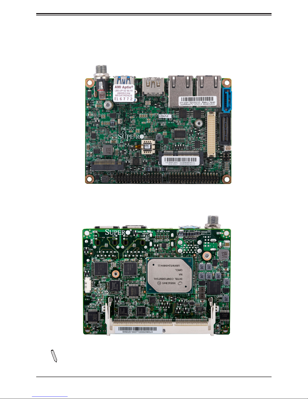
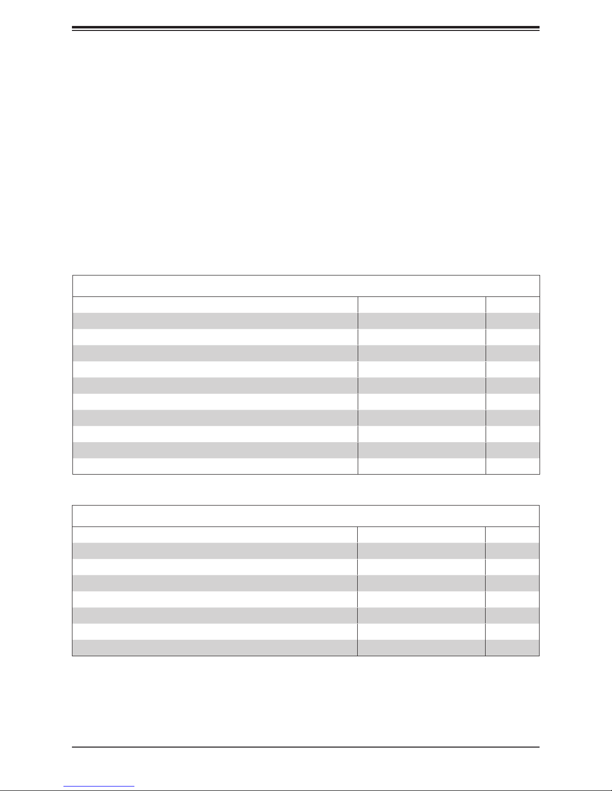
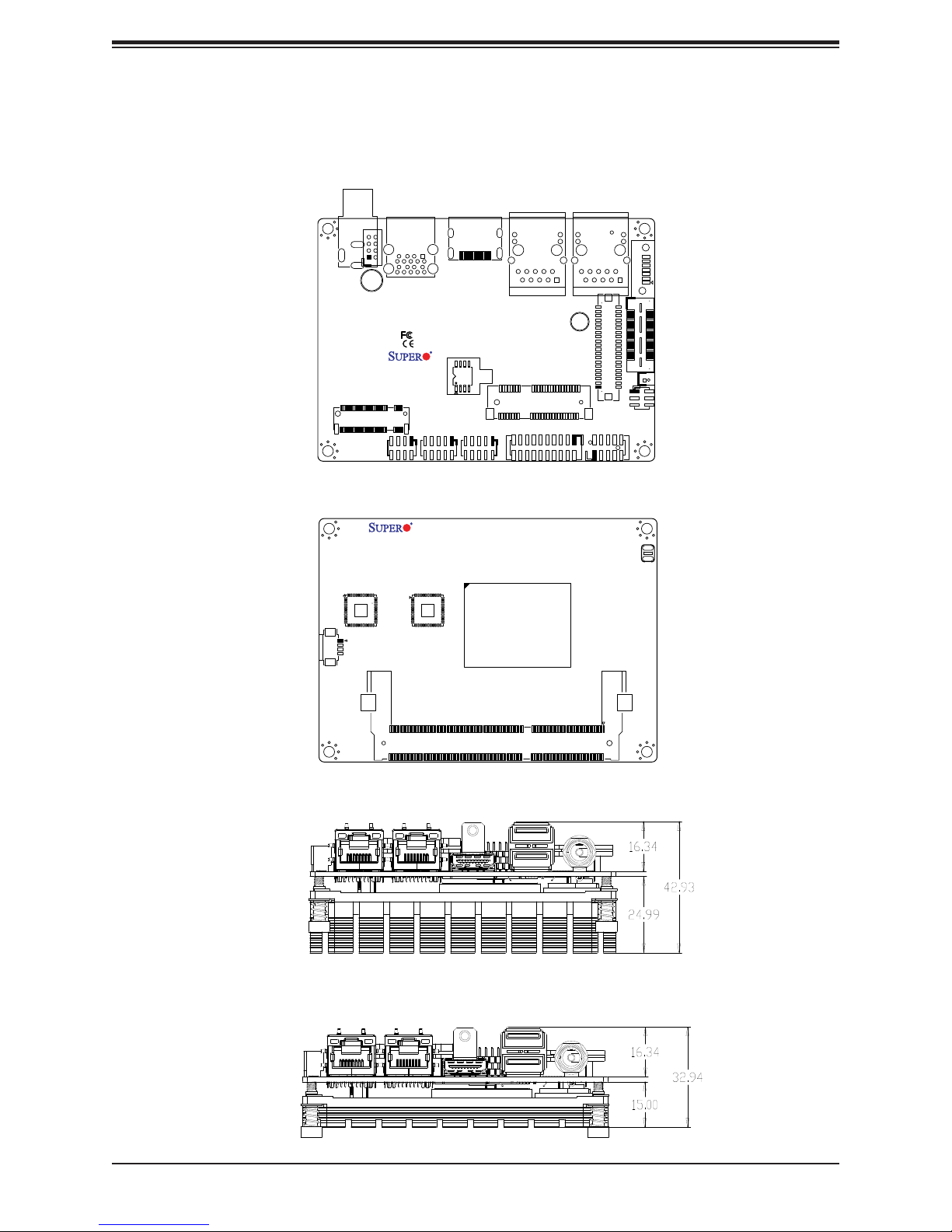
Figure 1-1. A2SAP-H Motherboard Image
Motherboard Top Side
Chapter 1: Introduction
Motherboard Bottom Side
Note: All graphics shown in this manual were based upon the latest PCB revision
available at the time of publication of the manual. The motherboard you received may
or may not look exactly the same as the graphics shown in this manual.
9
A2SAP-H/-E/-L User's Manual
Figure 1-2. A2SAP-E/-L Motherboard Image
Motherboard Top Side
Motherboard Bottom Side
10
Chapter 1: Introduction
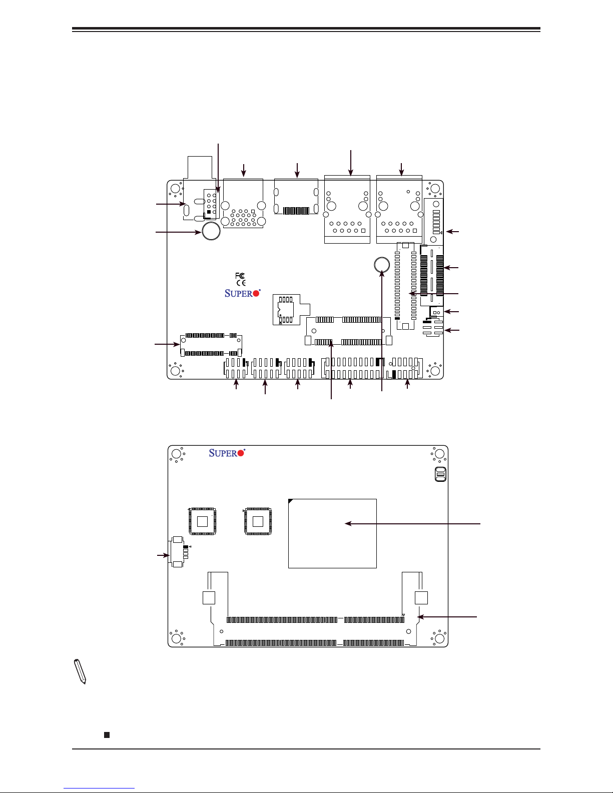
Figure 1-3. Motherboard Layout
(not drawn to scale)
A2SAP-H/-E Top Layout
JPWR1
JGP1
JHDMI1
A2SAP-L
Rev:1.00
DESIGNED IN USA
J6
JLAN2
JMP1
JLAN1
SRW1
JCOM1
JDC
JUSB1
SRW2
JMD1
JF1
A2SAP-L Bottom Layout
LVDS1
J3
JEIO1
BT1
JLCDPWR1
PEC1
I-SATA1
1
CPU1
JSMBUS1
J5
A2SAP-H/-E Back Panel I/O with Heatsink
A2SAP-L Back Panel I/O with Heatsink
11
A2SAP-H/-E/-L User's Manual
Quick Reference
Top Layout
JDC
SRW2
JMD1
JDC
JPWR1
JPWR1
SRW2
JMD1
JF1
JUSB1
JUSB1
JF1
JGP1
JGP1
JHDMI1
JHDMI1
A2SAP-L
Rev:1.00
DESIGNED IN USA
J6
J6
JMP1
JLAN2
JLAN2
JMP1
JCOM1
JCOM1
SRW1
JLAN1
SRW1
JLAN1
LVDS1
J3
J3
JEIO1
BT1
JLCDPWR1
1
I-SATA1
I-SATA1
JEIO1
LVDS1
BT1
JLCDPWR1
Bottom Layout
PEC1
CPU1
CPU
JSMBUS1
JSMBUS1
J5
SODIMM
Notes:
• See Chapter 2 for detailed information on jumpers, I/O ports, and JF1 front panel connec-
tions. Jumpers and LED indicators not indicated are used for testing only.
• " " indicates the location of Pin 1.
12

Chapter 1: Introduction
Quick Reference Table
Jumper Description Jumper Setting (Default *)
FORCE POWER ON
JLCDPWR1
LVDS Panel Power Source Selection
Connector Description
BT1
I-SATA1 Intel® PCH SATA 3.0 Port
J3 Front Panel Audio Header (Mic-In/Line-out)
J6 Two USB 2.0 Headers
JCOM1 Two COM Headers (two RS232/422/485)
JDC 12V DC Jack Power Connector (for A2SAP-H)
JEIO1
JF1 Front Control Panel Header (Power/HDD LED, Reset, Power button)
JGP1 8-bit General Purpose I/O Header
JHDMI1 High Denition Multimedia Interface (HDMI) Port
JLAN1/JLAN2 LAN1/LAN2 (RJ45 LAN) Ports
JMD1 M.2 Slot (B-KEY 2242/3042) (SATA 3.0 / PCI-E / USB 2.0)
JMP1 Mini PCI-E Slot (supports two PCIe Gen2 / one USB 2.0)
JPWR1 Two 4-pin 12V Power Connectors (for A2SAP-E/-L)
Battery Connector
(To Clear CMOS, remove the battery, short pins 1-2 and install the battery.)
Supermicro Extension I/O
(HDMI/DP, two PCI-E x1, two USB 2.0, LPC, SATA, SMBus, Power)
Pins 2-4* (FORCE POWER ON)
Pins 4-6 (POWER BUTTON ON)
Pins 1-3* (3.3V)
Pins 3-5 (5V)
JSMBUS1 SMBus and 5V SATA Power Box Header
JUSB1 Two Back Panel USB 3.0 Ports
LVDS1 Dual Channel 48-bit LVDS Connector
SRW1 ~ SRW2 M.2 and Mini PCI-E Mounting Holes
Note: Components not documented are for internal testing only.
13
A2SAP-H/-E/-L User's Manual
Motherboard Features
Motherboard Features
CPU
• A2SAP-H/-E: Intel® Atom™ x5-E3940 Processor, Quad Core, 2M Cache, 1.6GHz-1.8GHz, 9.5W
• A2SAP-L: Intel® Atom™ x5-E3930 Processor, Dual Core, 2M Cache, 1.3GHz-1.8GHz, 6.5W
Memory
• Integrated memory controller supports up to 8GB of DDR3L 1867MHz Non-ECC 204-pin SO-DIMM
DIMM Size
• Up to 8GB at 1.35V
Expansion Slots
• One (1) Half Size Mini PCI-Express slot (PCI-E/USB 2.0)
• One (1) M.2 B-Key 3042/2242 (PCI-E/SATA/USB 2.0)
Network
• Dual Intel I210 controller
Graphics
• Features: OpenGL 5.0, DirectX 12, OpenCL 2.1
• Hardware Decode: AVC/H.264, MPEG2, VC1/WMV9, JPEG/MJPEG,
• Intel® HD Graphics GT Series
HEVC/H.265, VP8, VP9, MVC
• Hardware Encode: AVC/H.264, JPEG/MJPEG, HEVC/H.265, VP8, VP9, MVC
• Display: HDMI 1.4 (resolution up to 3840x2160 at 30Hz), LVDS (dual channel
48-bit, resolution up to 1920x1200 at 60Hz)
I/O Devices
• COM Header • Two (2) front accessible ports (JCOM1 supports two RS232/RS422/RS485)
• SATA Port • One (1) SATA 3.0 port (I-SATA1)
• Audio Port
• SMBus Header
• SMCI EI/O
• One (1) HD Audio header with Mic-in/Line-out (Realtek ALC888S) (Audio on
A2SAP-H/-E/-L only supports 0-60ºC)
• One (1) SMBus box header
• One (1) Supermicro I/O Header (HDMI, Two PCI-E x1, Two USB 2.0, LPC,
SATA, SMBus, Power)
Peripheral Devices
• One (1) USB 3.0 port on the rear I/O panel (JUSB1)
• One (1) USB 2.0 header (J6)
BIOS
• 128Mb SPI AMI BIOS
®
• ACPI 3.0, SMBIOS 2.7, PCI F/W 3.0, BIOS rescue hot-key, RTC (Real Time Clock) wakeup
Note: The table above is continued on the next page.
14
Chapter 1: Introduction
Motherboard Features
Power Management
• ACPI power management
• S3, S4, S5
• Power button override mechanism
• Power-on mode for AC power recovery
• Wake-On-LAN
• TXE Management Engine
• Force Power On by Jumper
• RTC Battery (typical voltage: 3.0V, normal discharge capacity: 210mAh)
System Health Monitoring
• Onboard voltage monitoring for +3.3V, +5V, +3.3V standby, VBAT, Vcore, system temperature, and memory temperature
• CPU switching phase voltage regulator
• CPU thermal trip support
System Management
• Trusted Platform Module (TPM) 1.2/2.0 support (supported by the Supermicro E I/O, JEIO1, header)
• SuperDoctor® 5, Watch Dog, NMI, RoHs
LED Indicators
• Power LED
• HDD Activity LED
• LAN Activity LED
Dimensions
• 2.83" (L) x 3.93" (W) (72mm x 100mm) SBCs
• Height: A2SAP-H/-E 42.93mm, A2SAP-L 32.94mm
Environment
• Operating Temperature Range: A2SAP-H/-E/-L support -30°C ~ 75°C (-22°F - 167°F)
• Non-Operating Temperature Range: -40°C - 85°C (-40°F - 185°F)
• Operating Relative Humidity Range: 8% - 90% (non-condensing)
• Non-Operating Relative Humidity Range: 10% - 95% (non-condensing)
Note 1: The CPU maximum thermal design power (TDP) is subject to chassis and
heatsink cooling restrictions. For proper thermal management, please check the chas-
sis and heatsink specications for proper CPU TDP sizing.
15
A2SAP-H/-E/-L User's Manual
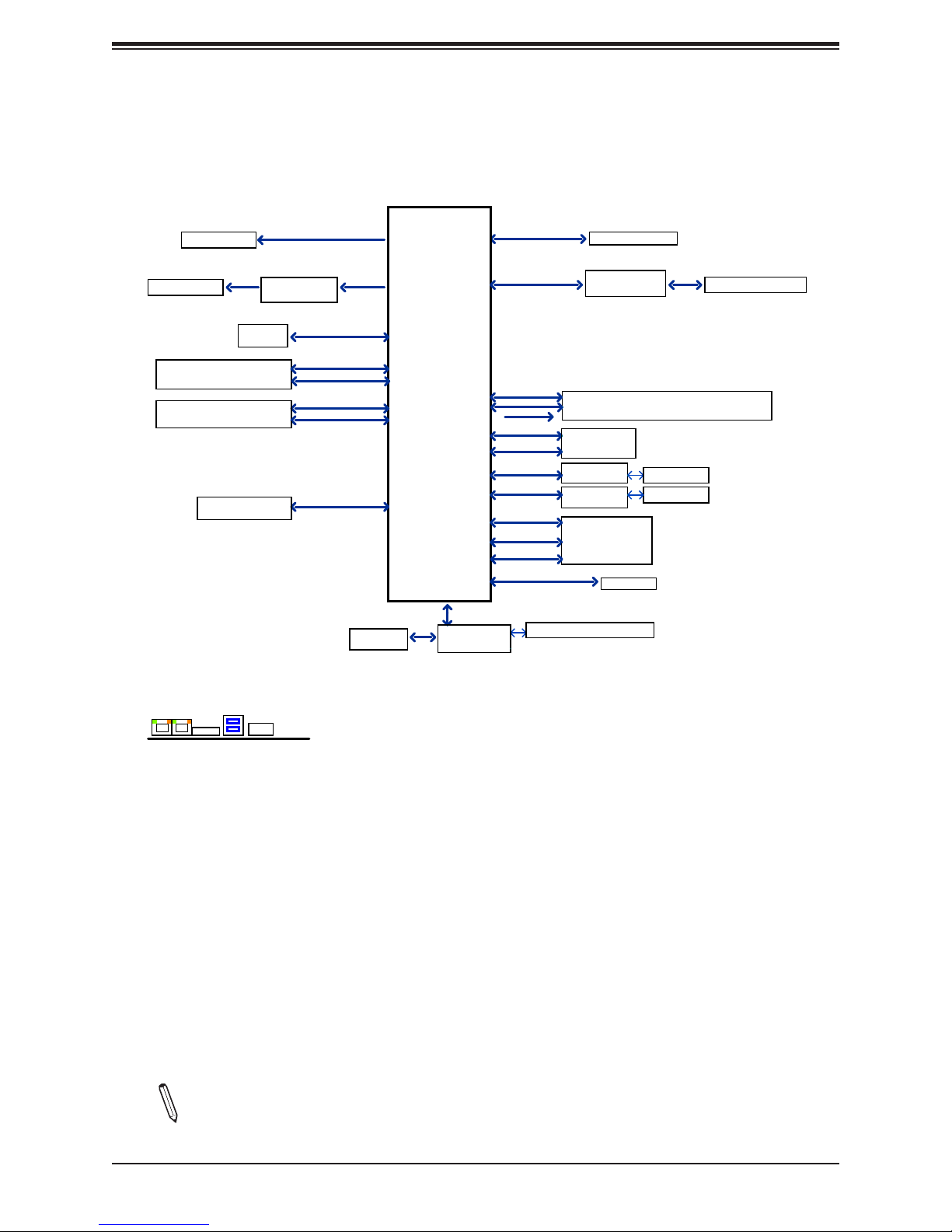
Figure 1-3.
System Block Diagram
HDMI connector
LVDS Connector
Rear USB3.0 connector (USB 0)
Rear USB3.0 connector (USB 1)
Rear USB3.0 connector (USB 2)
Rear USB3.0 connector (USB 3)
SMBUS_HEADER
I/O Panel Layout
USB 3.0
LAN1 LAN2
USB 3.0
HDMI
21
DP to LVDSBridge
FLASH
SPI 128Mb
DC_IN
PTN3460
DDI0
SPI
5.0Gb/s
5.0Gb/s
480Mb/s
480Mb/s
SMBUS
eDP
GPIO
Intel
DDR3L non ECC SKU
FST_SPI
USB 2.0 [0]
USB 3.0 [0]
USB 2.0 [1]
USB 3.0 [1]
USB 2.0 [2]
USB 3.0 [3]
LPC
PCIE[4/5]
PCIE[3]
USB2.0[7]
PCIE[2]
PCIE[1]
PCIE[0]
SATA[1]
USB2.0[6]
SATA[0]
NCT5523
Audio
SIO
DUAL CHANNEL
DDR3L 1866 MHz
High Definition
PCIe Gen2 x 2
DDI1
PCIe Gen2 x 1
5.0GT/s
480Mb/s
GBE
2.5GT/s
PCIe Gen2 x 1
5.0GT/s
PCIe Gen2 x 1
5.0GT/s
SATA
6Gb/s
480Mb/s
GLAN2 (LAN2)
INTEL I210
GLAN2 (LAN1)
INTEL I210
SATA 6Gb/s
COM 1 / 2 (RS232 / 422/ 485)
MAX. 8G SO-DIMM SUPPORTED
Non-ECC-SODIMM0
REALTEK
ALC888S-VD2-GR
EIO (PCIE / USB2.0 / LPC (PORT80) / SATA/SMB
(HDMI / DP)
Mini-PCIe Slot
RJ45 (JLAN2)
RJ45 (JLAN1)
M.2 SLOT (B KEY)
I-SATA0
FRONT AUDIO Header
Note: This is a general block diagram and may not exactly represent the features on
your motherboard. See the previous pages for the actual specications of your motherboard.
16

Chapter 1: Introduction
1.2 Processor Overview
Built upon the functionality and capability of the Intel® Atom SoC series processor, the
A2SAP-H/-E/-L motherboard offers maximum I/O expandability, energy efciency, and data
reliability in a 14-nm process architecture, and is optimized for embedded storage solutions,
networking applications, or cloud-computing platforms. The A2SAP-H/-E/-L drastically
increases system performance for a multitude of server applications.
The A2SAP-H/-E/-L supports the following features:
• Intel Virtualization Technology for Directed I/O (Intel VT-d)
• Enhanced Intel SpeedStep® Technology
• Video Connectors: HDMI and LVDS
• Adaptive Thermal Management/Monitoring
• Mini-PCI-E slot with PCI-E Gen2 X1 with transfer rates of up to 5Gb/s
• SATA port with SATA Gen3 with transfer rates of up to 6Gb/s
• System Management Bus (SMBus) Specication, Version 2.0
• M.2 slot with B-key 2242/3042 module is supported by an extender bracket
• Integrated Sensor Hub (ISH)
• Intel® Identity Protection Technology
1.3 Special Features
This section describes the health monitoring features of the A2SAP-H/-E/-L motherboard.
The motherboard has an onboard System Hardware Monitor chip that supports system health
monitoring.
Recovery from AC Power Loss
The Basic I/O System (BIOS) provides a setting that determines how the system will respond
when AC power is lost and then restored to the system. You can choose for the system to
remain powered off (in which case you must press the power switch to turn it back on), or
for it to automatically return to the power-on state. See the Advanced BIOS Setup section
for this setting. The default setting is Last State.
17

A2SAP-H/-E/-L User's Manual
1.4 ACPI Features
ACPI stands for Advanced Conguration and Power Interface. The ACPI specication denes
a exible and abstract hardware interface that provides a standard way to integrate power
management features throughout a computer system including its hardware, operating system
and application software. This enables the system to automatically turn on and off peripherals
such as network cards, hard disk drives and printers.
In addition to enabling operating system-directed power management, ACPI also provides a
generic system event mechanism for Plug and Play and an operating system-independent
interface for conguration control. ACPI leverages the Plug and Play BIOS data structures
while providing a processor architecture-independent implementation that is compatible with
Windows® 10.
1.5 Power Supply
As with all computer products, a stable power source is necessary for proper and reliable
operation. It is even more important for processors that have high CPU clock rates. In areas
where noisy power transmission is present, you may choose to install a line lter to shield
the computer from noise. It is recommended that you also install a power surge protector to
help avoid problems caused by power surges.
1.6 Super I/O
The Super I/O (NCT5523 chip) includes a data separator, write pre-compensation circuitry,
decode logic, data rate selection, a clock generator, drive interface control logic and interrupt
and DMA logic. The wide range of functions integrated onto the Super I/O greatly reduces
the number of components required for interfacing with oppy disk drives.
The Super I/O provides two high-speed, 16550 compatible serial communication ports
(UARTs), one of which supports serial infrared communication. Each UART includes a 16-byte
send/receive FIFO, a programmable baud rate generator, complete modem control capability
and a processor interrupt system. Both UARTs provide legacy speed with baud rate of up to
115.2 Kbps as well as an advanced speed with baud rates of 250 K, 500 K, or 1 Mb/s, which
support higher speed modems.
The Super I/O provides functions that comply with ACPI (Advanced Conguration and Power
Interface), which includes support of legacy and ACPI power management through a SMI
or SCI function pin. It also features auto power management to reduce power consumption.
The IRQs, DMAs and I/O space resources of the Super I/O can be exibly adjusted to meet
ISA PnP requirements, which support ACPI and APM (Advanced Power Management).
18

Chapter 1: Introduction
1.7 Advanced Power Management
The following new advanced power management features are supported by the motherboard.
Management Engine (ME)
Intel Atom SoC only supports the TXE function, also called CSE (Converged Security Engine),
which is the lite ME function.
19

A2SAP-H/-E/-L User's Manual
Chapter 2
Installation
2.1 Static-Sensitive Devices
Electrostatic Discharge (ESD) can damage electronic com ponents. To prevent damage to your
motherboard, it is important to handle it very carefully. The following measures are generally
sufcient to protect your equipment from ESD.
Precautions
• Use a grounded wrist strap designed to prevent static discharge.
• Touch a grounded metal object before removing the board from the antistatic bag.
• Handle the board by its edges only; do not touch its components, peripheral chips, memory
modules or gold contacts.
• When handling chips or modules, avoid touching their pins.
• Put the motherboard and peripherals back into their antistatic bags when not in use.
• For grounding purposes, make sure that your chassis provides excellent conductivity be-
tween the power supply, the case, the mounting fasteners and the motherboard.
• Use only the correct type of CMOS onboard battery as specied by the manufacturer. Do
not install the CMOS battery upside down, which may result in a possible explosion.
Unpacking
The motherboard is shipped in antistatic packaging to avoid static damage. When unpacking
the motherboard, make sure that the person handling it is static protected.
20
Chapter 2: Installation
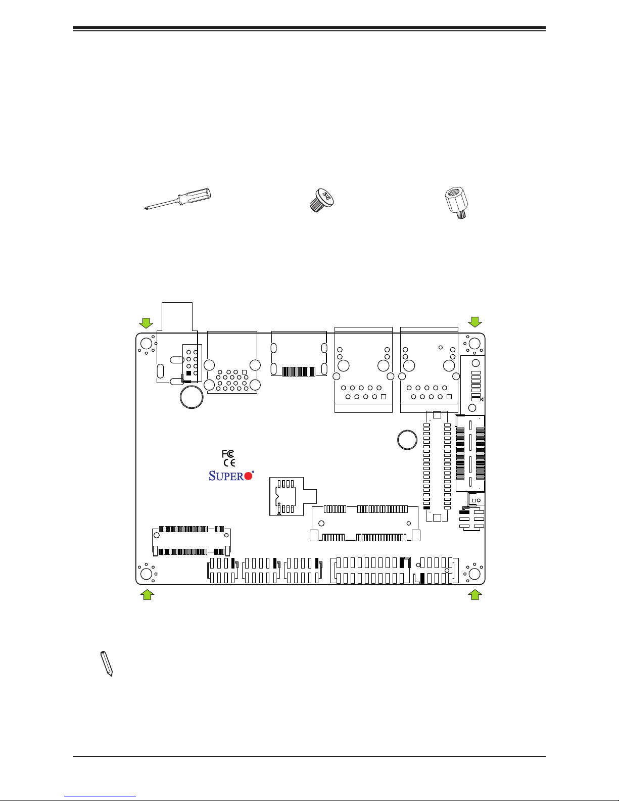
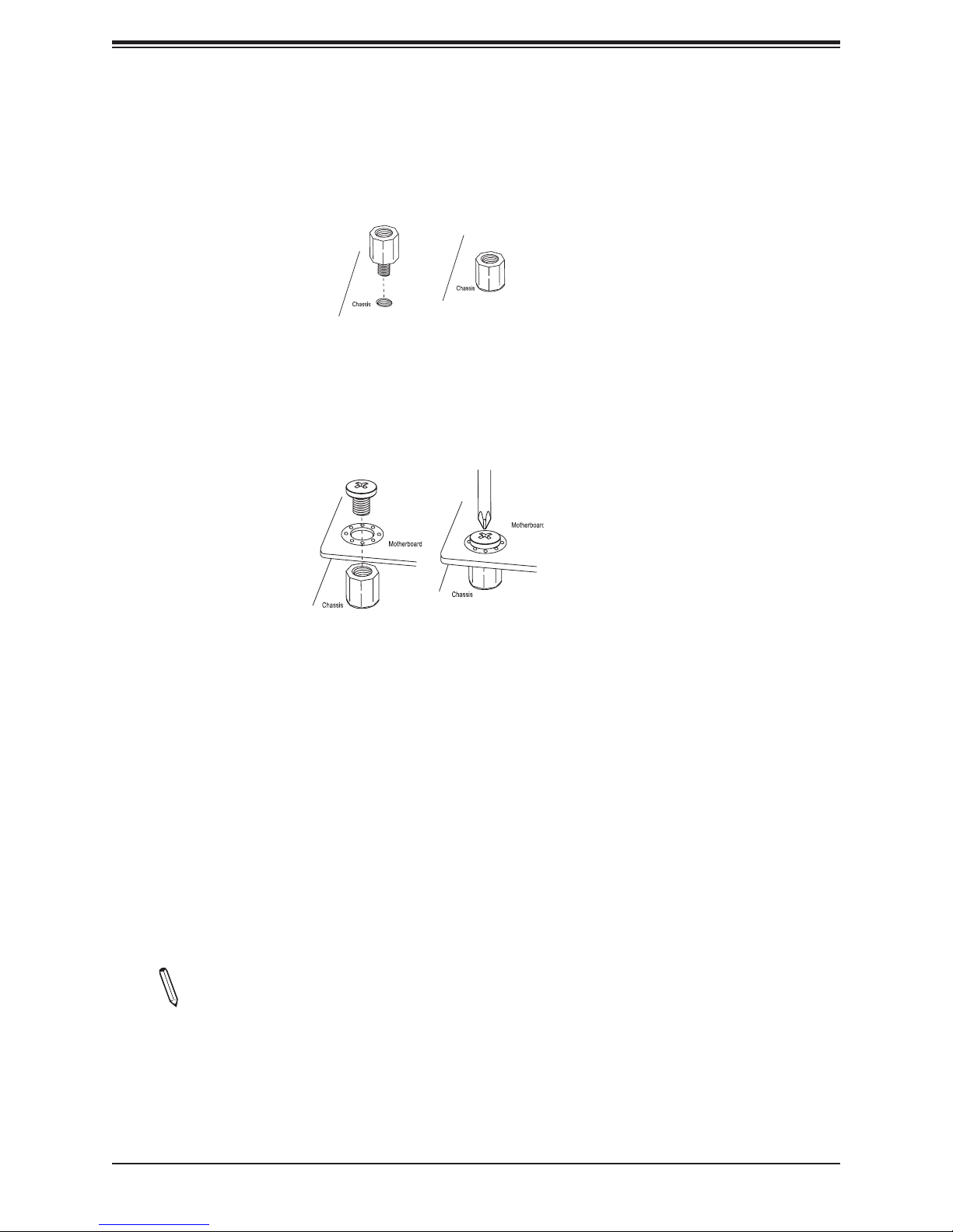
2.2 Motherboard Installation
All motherboards have standard mounting holes to t different types of chassis. Make sure
that the locations of all the mounting holes for both the motherboard and the chassis match.
Although a chassis may have both plastic and metal mounting fasteners, metal ones are
highly recommended because they ground the motherboard to the chassis. Make sure that
the metal standoffs click in or are screwed in tightly.
Phillips Screwdriver (1)
Tools Needed
JPWR1
JDC
SRW2
JMD1
JUSB1
Phillips Screws (4)
JHDMI1
A2SAP-L
Rev:1.00
DESIGNED IN USA
JGP1
J6
JLAN2
JMP1
JCOM1
SRW1
Standoffs (4)
Only if Needed
JLAN1
JEIO1
LVDS1
BT1
JLCDPWR1
J3
I-SATA1
1
JF1
Location of Mounting Holes
Note: 1) To avoid damaging the motherboard and its components, please do not use
a force greater than 8 lb/inch on each mounting screw during motherboard installation.
2) Some components are very close to the mounting holes. Please take precautionary
measures to avoid damaging these components when installing the motherboard to
the chassis.
21
A2SAP-H/-E/-L User's Manual
Installing the Motherboard
1. Locate the mounting holes on the motherboard. See the previous page for the location.
2. Locate the matching mounting holes on the chassis. Align the mounting holes on the
motherboard against the mounting holes on the chassis.
3. Install standoffs in the chassis as needed.
4. Install the motherboard into the chassis carefully to avoid damaging other motherboard
components.
5. Using the Phillips screwdriver, insert a Phillips head #6 screw into a mounting hole on
the motherboard and its matching mounting hole on the chassis.
6. Repeat Step 5 to insert #6 screws into all mounting holes.
7. Make sure that the motherboard is securely placed in the chassis.
Note: Images displayed are for illustration only. Your chassis or components might
look different from those shown in this manual.
22
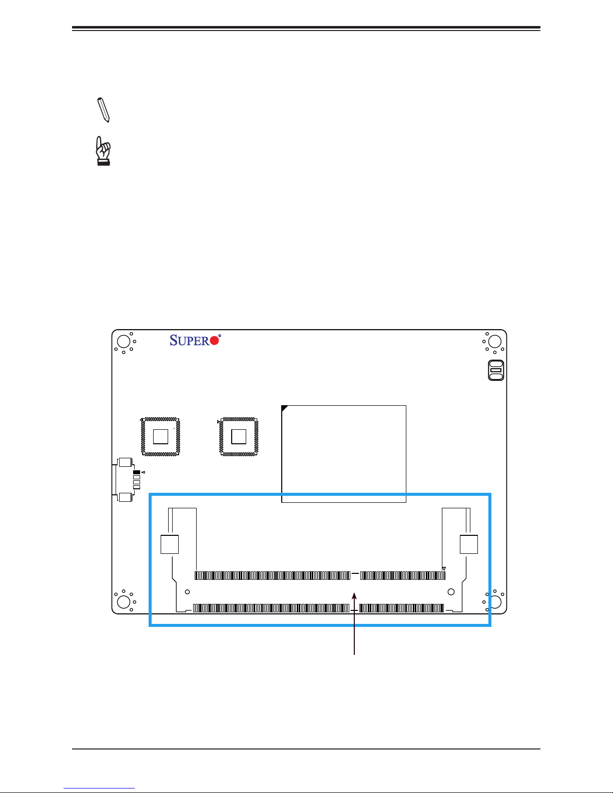
Chapter 2: Installation
2.3 Memory Support and Installation
Note: Check the Supermicro website for recommended memory modules.
Important: Exercise extreme care when installing or removing DIMM modules to pre-
vent any possible damage.
Memory Support
The A2SAP-H/-E/-L supports up to 8GB of DDR3L Non-ECC SO-DIMM with speeds of up to
1867MHz in one memory slot on the bottom side of the motherboard.
Bottom Layout
JSMBUS1
PEC1
CPU1
J5
SO-DIMM Socket
23
A2SAP-H/-E/-L User's Manual
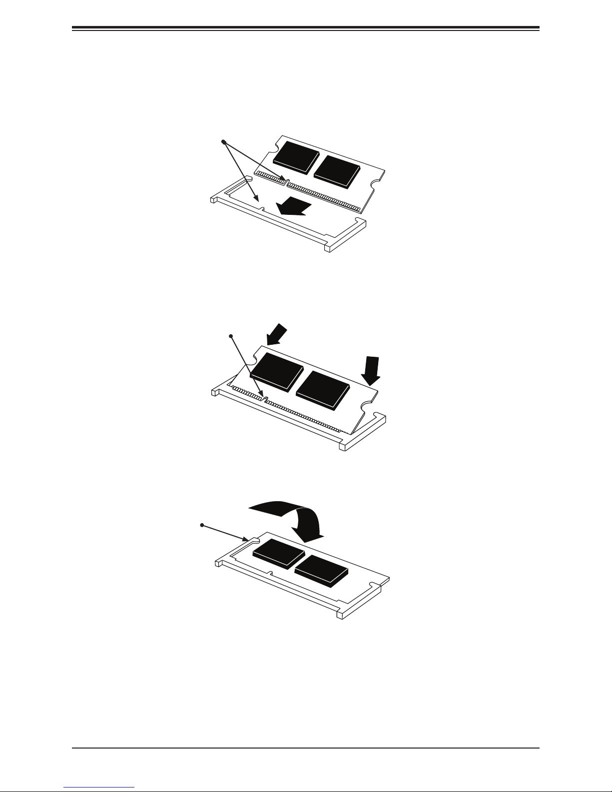
SO-DIMM Installation
1. Position the SO-DIMM module's bottom key so it aligns with the receptive point on the
slot.
Align
2. Insert the SO-DIMM module vertically at about a 45 degree angle. Press down until the
module locks into place.
Insert this end rst Press down until the module
locks into place.
3. The side clips will automatically secure the SO-DIMM module, locking it into place.
Locking clip
SO-DIMM Removal
1. Push the side clips at the end of the slot to release the SO-DIMM module. Pull the SODIMM module up to remove it from the slot.
24
Chapter 2: Installation
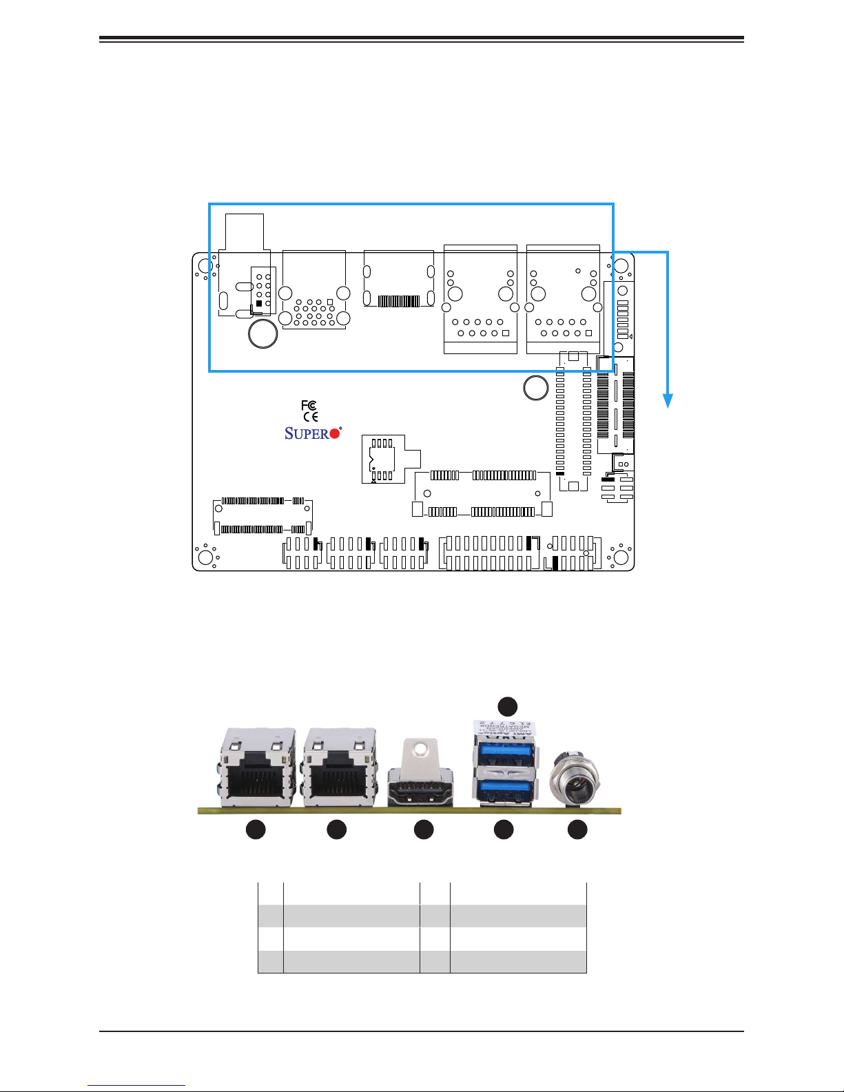
2.4 Rear I/O Ports
See Figure 2-1 below for the locations and descriptions of the various I/O ports on the rear
of the motherboard.
JPWR1
JDC
JUSB1
SRW2
JMD1
JGP1
JF1
JHDMI1
A2SAP-L
Rev:1.00
DESIGNED IN USA
J6
JLAN2
SRW1
JMP1
JCOM1
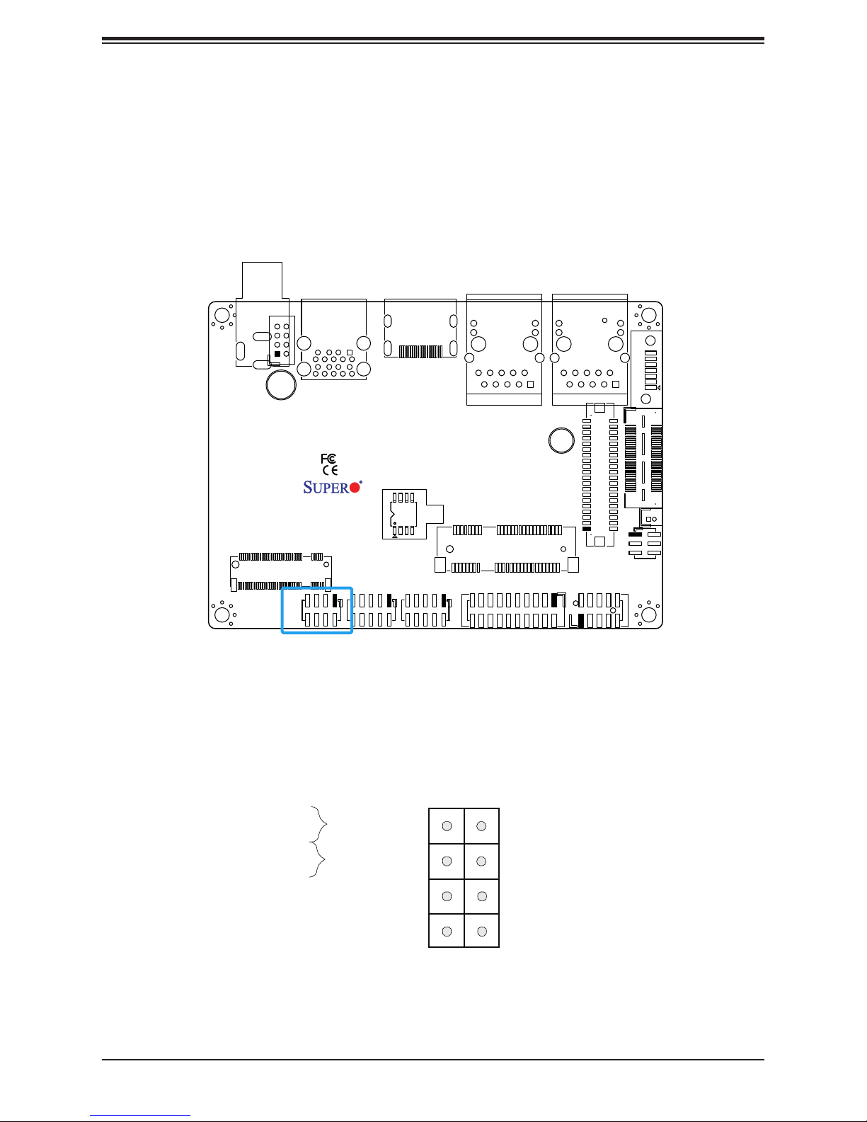
Figure 2-1. I/O Port Locations and Denitions
4
JLAN1
LVDS1
J3
JEIO1
BT1
JLCDPWR1
I-SATA1
1
1
# Description # Description
1. LAN1 4 USB2
2. LAN2 5 USB1
3 HDMI1 6 JDC
6532
25
A2SAP-H/-E/-L User's Manual
LAN Ports
Two LAN ports (JLAN1 - JLAN2) are located on the I/O back panel. These ports accept RJ45
type cables. Please refer to the LED Indicator section for LAN LED information. Refer to the
table below for pin dentions.
LAN Port
Pin Denition
Pin# Denition Pin# Denition
1 TD1+ 11 YEL-
2 TD1- 12 YEL+
3 TD2+ 13 GRN-/ORG+
4 TD2- 14 GRN+/ORG-
5 CT_VCC 15
6 CT_VCC 16
7 TD3+ 17
8 TD3- 18
9 TD4+ 19
10 TD4- 20
HDMI Port
The HDMI (High-Denition Multimedia Interface) port is used to display both high denition
video and digital sound through an HDMI-capable display, using the same cable.
3
2
1
1. JLAN1
JPWR1
2. JLAN2
3. HDMI
JDC
JUSB1
SRW2
JMD1
JGP1
JF1
JHDMI1
A2SAP-L
Rev:1.00
DESIGNED IN USA
J6
JLAN2
JMP1
JCOM1
SRW1
JLAN1
LVDS1
J3
JEIO1
BT1
JLCDPWR1
I-SATA1
1
26
Chapter 2: Installation
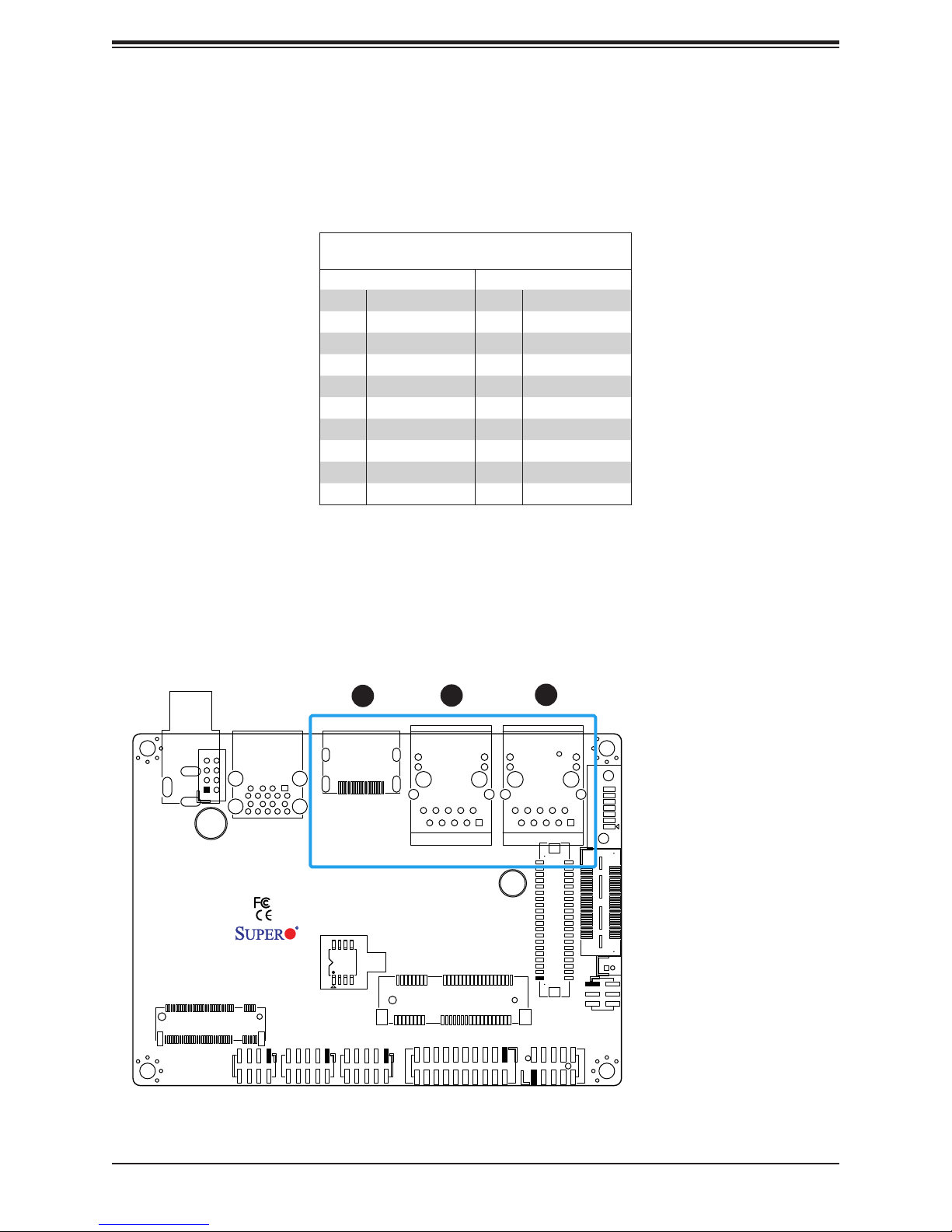
Universal Serial Bus (USB) Ports
There are two USB 3.0 ports (JUSB1) on the I/O back panel. The motherboard has two
additional USB 2.0 connections via the JEIO1 header. J6 also provides two front panel USB
2.0 connections. The onboard headers can be used to provide front side USB access with a
cable. Two USB 2.0 cables for front panel support are included with the motherboard.
Back Panel USB 3.0
Pin Denition
Pin# Denition Pin# Denition
A1 VBUS B1 VBUS
A2 D1-N B2 D2-N
A3 D1-P B3 D2-P
A4 GND B4 GND
A5 Stda_SSRX1-N B5 Stda_SSRX2-N
Pin# Denition Pin# Denition
1 P5V_DUAL_F 2 P5V_DUAL_F
3 USBCON_N4 4 USBCON_N5
5 USBCON_P4 6 USBCON_P5
7 Ground 8 Ground
9 NC 10 NC
A6 Stda_SSRX1-P B6 Stda_SSRX2-P
A7 GND_DRAIN B7 GND_DRAIN
A8 Stda_SSTX1-N B8 Stda_SSTX2-N
A9 Stda_SSTX1-P B9 Stda_SSTX2-P
JDC
This is a DC jack that functions as the 12V power connector.
12V Stdby Power
Pin Denition
Pin# Denition
1 P12VSB
2 GND
3 GND
Front Panel USB 2.0 Header
Pin Denition
JDC
2
JPWR1
SRW2
JMD1
1
1. JUSB1
2. JDC
JHDMI1
JUSB1
JLAN2
A2SAP-L
Rev:1.00
DESIGNED IN USA
JMP1
JGP1
JF1
J6
JCOM1
JLAN1
SRW1
LVDS1
JLCDPWR1
J3
JEIO1
BT1
I-SATA1
1
27
A2SAP-H/-E/-L User's Manual
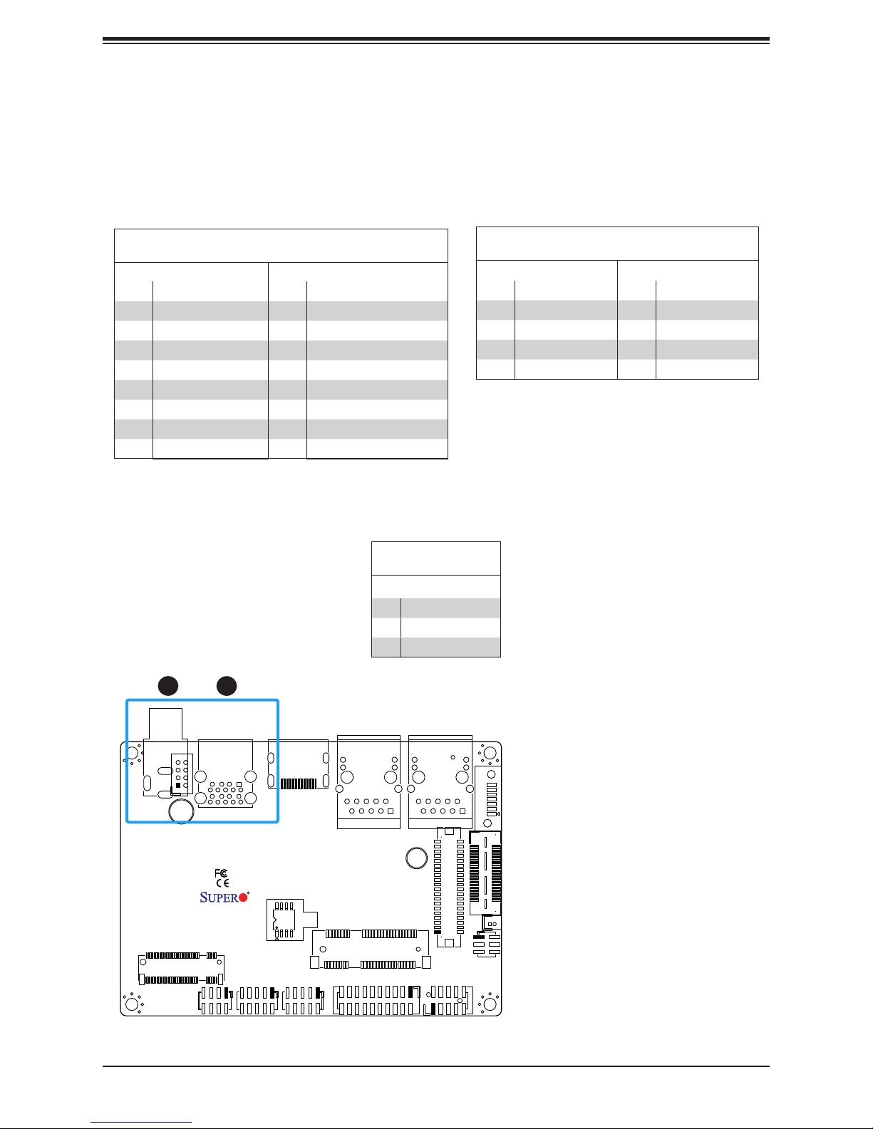
2.5 Front Control Panel
JF1 contains header pins for various buttons and indicators that are normally located on a
control panel at the front of the chassis. These connectors are designed specically for use
with Supermicro chassis. Refer to the gure below for the descriptions of the front control
panel buttons and LED indicators.
JPWR1
JDC
SRW2
JMD1
JF1
JHDMI1
JUSB1
JLAN2
A2SAP-L
Rev:1.00
DESIGNED IN USA
JMP1
JGP1
J6
JCOM1
Figure 2-2. JF1 Header Pins
SRW1
JLAN1
LVDS1
J3
JEIO1
BT1
JLCDPWR1
I-SATA1
1
PWR
Reset
Power Button
Reset Button
3.3V
3.3V Stby
1
78
28
2
Ground
Ground
HDD LED
Power LED
 Loading...