

Page 1
S
UPERMICR
R
ContaCt InformatIon
MNL-1561-QRG
• www.supermicro.com(Email:support@supermicro.com)
• Manuals:http://www.supermicro.com/support/manuals
• Drivers&Utilities: ftp://ftp.supermicro.com
• Safety:http://www.supermicro.com/about/policies/safety_information.cfm
© 2012 Supermicro Computer Inc. All rights reserved. Reproduction of this document whether in part or in whole is strictly prohibited without Supermicro's written
consent. All Trademarks are property of their respective entities. All information provided is deemed accurate at the time of printing; however, it is not guaranteed.
PaCkage Contents
(Appliestoindividual-packonly)
a1sam / a1srm motherboard serIes
QuICk referenCe guIde
• One(1)Supermicro Motherboard
• Six(6)SATACables
• One(1)I/O Shield
• One(1)Quick ReferenceGuide
MNL-1561-QRG
JPI2C1
JL1
JOH1
JF1
JPW1
JLAN2 JLAN1
JBT1
LED8
LED7
JPK1
SP1
JBAT1
JWD1
JI2C2
JI2C1
JPG1
JPL1
JSD1
JTPM1
JIPMB1
JVGA1
JUIDB1
COM2
JD1
I-SATA1
I-SATA0
I-SATA5
I-SATA4
1
I-SATA3
I-SATA2
FAN3
FAN2
FAN1
CPU1 SLOT4 PCI-E 2.0 X4
USB6
LAN3/4 LED
LAN2/LAN4
DIMMB2
DIMMA2
USB0/1
BUZZER
IPMI_LAN
BATTERY
DIMMB1
CPU1 SLOT6 PCI-E 2.0 X8
LAN1/LAN3
DIMMA1
USB4/5
COM1
A1SAM/A1SRM Series
Rev. 1.01
USB 2/3
FPCTRL
LED3
BIOS
SoC Processor
BMC
PHY
JPUSB1
JSTBY1
PWRI2C
LED2
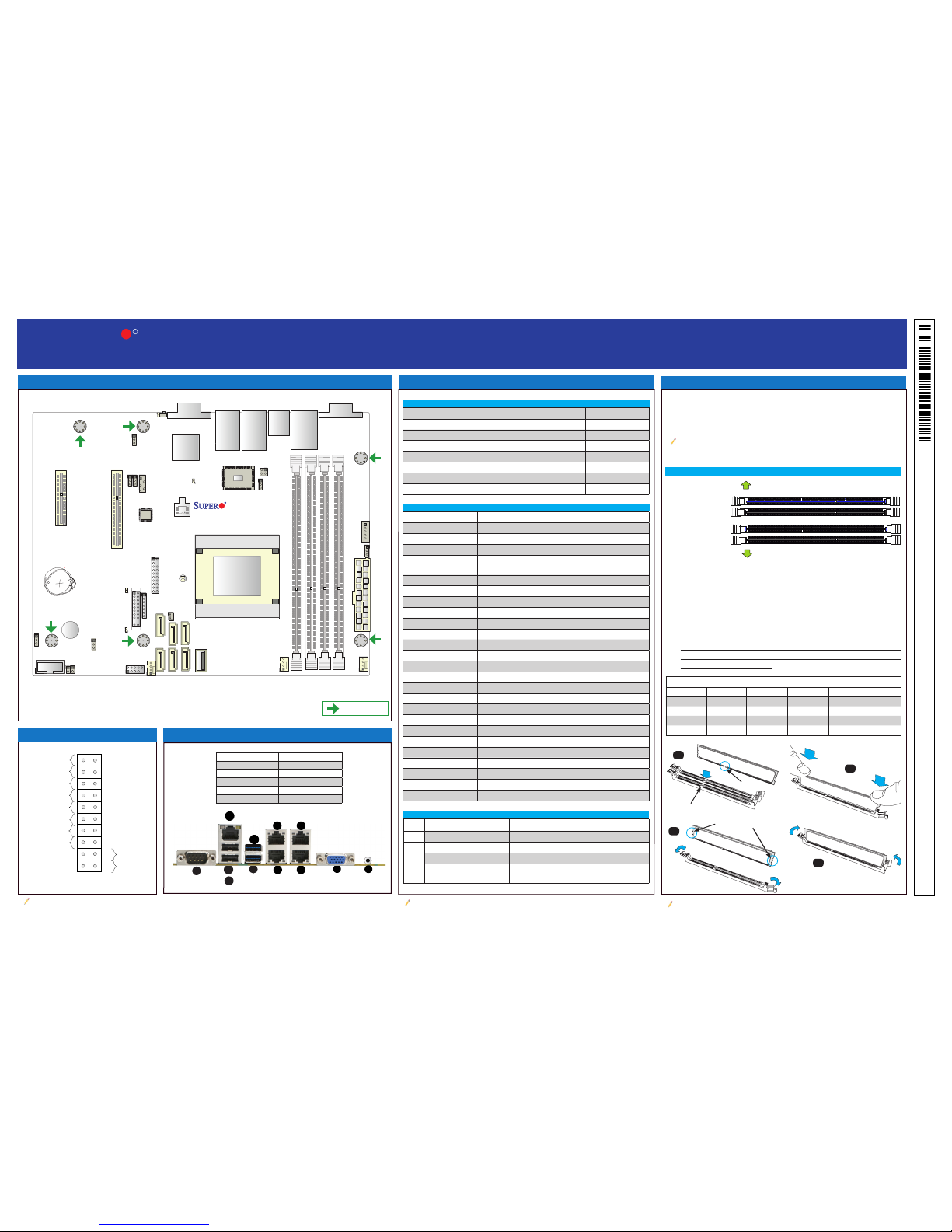
Jumpers, Connectors and LED Indicators
Back Panel I/O Connectors
Memory Support
Motherboard Layout and Features
Note: Graphics shown in this quick reference guide are for illustration only. Your components may or may not look exactly the same as drawings shown in this guide.
Note: Refer to Chapter 1 of the User Manual for detailed information on jumpers, connectors,
and LED indicators.
Note: Refer to Chapter 2 of the User Manual for detailed information on memory support and CPU/
motherboard installation instructions.
= mounting hole
Front Panel Control (JF1)
Jumpers
Connectors
LED Indicators
The A1SAM/A1SRM Series motherboard supp orts up to 64GB of D DR3 ECC
or Non-ECC Unbuf fered (UDIMM) 160 0/1333 MHz in x8 data width o nly, in 4
memory slots. Pop ulating these DIMM modules with a pai r of memory modules
of the same type and sa me size will result in better memory per formance.
Note: For memory optimization, use only DIMM modules that have been validated by Supermicro.
For the latest memory updates, please refer to our website a at http://www.supermicro.com/
products/motherboard.
Recommended Population (Balanced)
DIMMA1 Slot DIMMB1 Slot DIMMA2 Slot DIMMB2 Slot Total System Memory
4GB 4GB 8GB
4GB 4GB 4GB 4GB 16GB
8GB 8GB 16GB
8GB 8GB 8GB 8GB 32GB
DIMMA1 (Blue Slot)
DIMMA2
DIMMB2
DIMMB1 (Blue Slot)
Towards the edge of the motherboard
Towards the CPU
DIMM Memory Installation
A
C
B
E
D
G
I
K
F
H
J
L
A. COM1 G. LAN1
B. USB Port 2.0-0 H. LAN3
C. USB Port 2.0-1 I. LAN2
D. IPMI LAN J. LAN4
E. USB Port 2.0-2 K. VGA
F. USB Port 2.0-3 L. UID Switch
Connector Description
Battery Onboard Battery (JBAT1)
COM1/COM2 COM1/COM2 Port Headers
FAN1-FAN3 System Cooling Fans
JD1 Power LED/Speaker Header(Pins 1-3: Power LED, Pins 6-7: Internal
Buzzer, Pins 4-7: External Speaker)
JF1 Front Panel Control Header
JIPMB1 4-pin External SMbus I2C Header
JL1 Chassis Intrusion Header
JOH1 Overheat LED Header
JPI2C1 Power Supply System Management Bus (SMBus) I2C Header
JPK1 LAN3/LAN4 LED Indication Header
JPW1 24-pin ATX Power Connector
JSD1 SATA DOM (Device_On_Module) Power Connector
JSTBY1 5V Standby Power Connector
JTPM1 Trusted Platform Module (TPM)/Port 80 Connector
JUIDB1 Unit Identier (UID) Switch
LAN1/LAN3, LAN2/LAN4 Gigabit Ethernet (RJ45) Ports 1/3, 2/4
IPMI-LAN IPMI-dedicated LAN for IPMI 2.0 interface
I-SATA0-I-SATA5 (Intel) Serial ATA Ports 0-5
Slot4 PCI-E 2.0 x 4 slot
Slot6 PCI-E 2.0 x 8 slot
SP1 Internal Speaker/Buzzer
USB 0/1, 2/3 Backpanel USB 2.0 Por ts 0/1, 2/3
USB 4/5 Front Panel Accessible USB 2.0 Header USB (2.0) 4/5
USB 6 Type A USB6 Port (2.0)
VGA Back Panel VGA Port
LED Description Color/State Status
LED2 IPMI/BMC Heartbeat Green: Blinking Normal
LED3 Power LED Green: On System Power On
LED7 UID Switch LED Blue: On Unit Identied
LED8 Overheat/PWR Fail/Fan Fail LED Red: Solid on/Blinking
Solid On: Overheat,
Blinking: PWR Fail or Fan Fail
Jumper Description Default
JBT1 CMOS Clear Off (Normal)
JI2C1/JI2C2 SMB to PCI-Exp. Slots Pins 2-3 (Disabled)
JPG1 VGA Enable Pins 1-2 (Enabled)
JPL1 Ethernet LAN Ports Enable Pins 1-2 (Enabled)
JPUSB1 USB Wake_Up Enable Pins 1-2 (Enabled)
JWD1 Watch Dog Enable Pins 1-2 (Reset)
JD1 On Board Buzzer Pins 6-7 (Enabled)
Power Button
OH/Fan Fail/PWR Fail/
LED Cathode
1
NIC1 Link LED
Reset Button
2
Power Fail LED
HDD LED
FP PWRLED
Reset
PWR
3.3 V
3.3V Stby
UID LED Cathode
Ground
Ground
1920
3.3V
X
Ground
NMI
X
NIC2 Link LED
3.3V Stby
3.3V Stby
Memory Population Guidelines
When installing memory modules, the DIMM slots should be populated in the following
order: DIMMA1, DIMMB1, DIMMA2 and DIMMB2.
• Always use DDR3 DIMM modules of the same size, type and speed.
• The motherboard will support one DIMM module or three DIMM modules in-
stalled. However for best memory performance, install DIMM modules in pairs.
• Be sure to use memory modules of the same type, same speed, and same
frequency on the same motherboard. Mixing of memory modules of different
types and speeds is not allowed.
Module Notches
Module Key
Socket Key
1
2
3
4
 Loading...