SUMMIT SMH4044F Datasheet

1
Characteristics subject to change without notice 2057 1.x 8/16/01
SMH4044
SUMMIT
MICROELECTRONICS, Inc.
Preliminary
©SUMMIT MICROELECTRONICS, Inc., 2001 • 300 Orchard City Dr., Suite 131 • Campbell, CA 95008 • Phone 408-378-6461 • FAX 408-378-6586 • www.summitmicro.com
!!
!!
! IPMI Implementation
""
""
" IPMB Interface
""
""
" Software Controlled Power-Up/-Down
""
""
" Status Reporting: 5V, 3.3V, V1, V2, Healthy,
Signal Valid, Reset
""
""
" 2k-Bit E2PROM Memory
!!
!!
! Full Voltage Control for Hot Swap Applications
""
""
" Detect, Monitors and Controls up to 4 inde-
pendent supplies
!!
!!
! 14V High Side Driver Generation Allows use of
Low On Resistance N-Channel FETs
Compact PCI Hot-Swap Controller
With IPMI Support
FEATURES
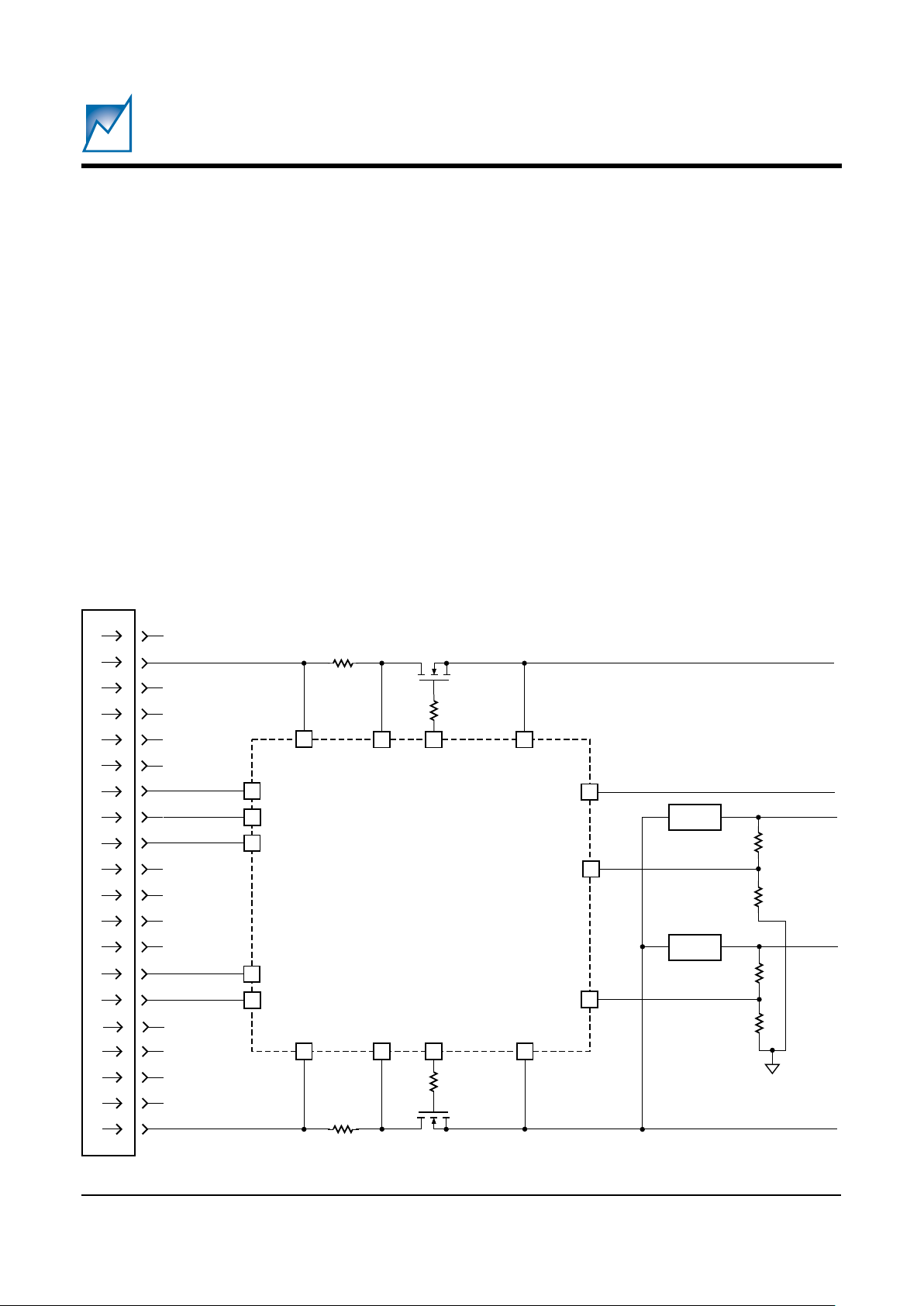
SIMPLIFIED APPLICATION DRAWING
!!
!!
! Under-Voltage Lockout
!!
!!
! Electronic Circuit Breakers
""
""
" Programmable Over-current Levels
!!
!!
! Card Insertion Detection
!!
!!
! Card Voltage Sequencing
!!
!!
! Flexible Reset Control
""
""
" Low Voltage Resets
""
""
" Host Reset Filtering
""
""
" Soft Reset
!!
!!
! Adjustable Power On Slew Rate
Simplified Application Drawing — Triple Voltage Hot Swap (12V, 5V, 3.3V)
1N4148
VCC
HST_
3V_MON
CARD_3V_MON
CARD_5V_MON
SGNL_VLD#
HEALTHY#
DRVREN#
VGATE5
VGATE3
GND
BD_SEL2#
BD_SEL1#
MONITOR1
MONITOR 2
CBI_3
CBI_5
LOCAL_PCI_RST
SMH4044
12V
5V
3.3V
10Ω
4.7kΩ
0.33µF
330kΩ
0.1µF
12V
5V
3.3V
CompactPCI
Backplane
2057 SAD-A
IPMB_SDA
IPMB_SCL
GAO
GA1
GA2
SDA
SCL
A0
A1
A2
26
27
42
44
7
11
41
6
12
20
16
15
18
19
35
36
30
29
33
34
40
45

2
SMH4044
2057 1.x 8/16/01
SUMMIT MICROELECTRONICS, Inc.
Preliminary
Simplified Application Drawing — Triple Voltage Hot Swap (5V, 3.3V, 1.8V)
DESCRIPTION
The SMH4044 is a fully integrated hot swap controller that
provides complete power control for add-in cards ranging
in use for basic hot swap systems to high availability
systems. It detects proper insertion of the card and
senses valid supply voltage levels at the backplane.
Utilizing external low on-resistance N-channel MOSFETs, card power is ramped by two high-side driver
outputs that are slew-rate limited at 250V/s.
The SMH4044 continuously monitors the host supplies,
the add-in card supplies and the add-in card currents. If
the SMH4044 detects the current is higher than the
programmed value it will shut down the MOSFETs and
issue a fault status to the host.
The internal 256 × 8 E
2
PROM can be used as configuration memory for the individual card or as general purpose
memory.
Programming of configuration, control and calibration
values by the user can be simplified with the interface
adapter and Windows GUI software obtainable from
Summit Microelectronics.
VCC
HST_3V_MON
CARD_3V_MON
CARD_5V_MON
SGNL_VLD#
HEALTHY#
VGATE5
VGATE3
GND
BD_SEL2#
BD_SEL1#
MONITOR1
MONITOR 2
CBI_3
CBI_5
LOCAL_PCI_RST
SMH4044
1.8V
5V
3.3V
1.8V
5V
3.3V
CompactPCI
Backplane
2057 SAD-B
42
44
41
6
20
16
15
18
19
35
36
30
29
33
34
40

3
2057 1.x 8/16/01
SMH4044
SUMMIT MICROELECTRONICS, Inc.
Preliminary
Simplified Application Drawing — Hot Swap with PUP LDO Sensing
VCC
HST_3V_MON
CARD_3V_MON
CARD_5V_MON
SGNL_VLD#
HEALTHY#
VGATE5
VGATE3
GND
BD_SEL2#
BD_SEL1#
MONITOR 2
CBI_3
CBI_5
LOCAL_PCI_RST
SMH4044
5V
3.3V
5V
3.3V
CompactPCI
Backplane
2057 SAD-C
MONITOR 1
LDO
LDO
2.8V
1.8V
42
44
41
6
20
16
15
18
19
35
36
30
29
33
34
40

4
SMH4044
2057 1.x 8/16/01
SUMMIT MICROELECTRONICS, Inc.
Preliminary
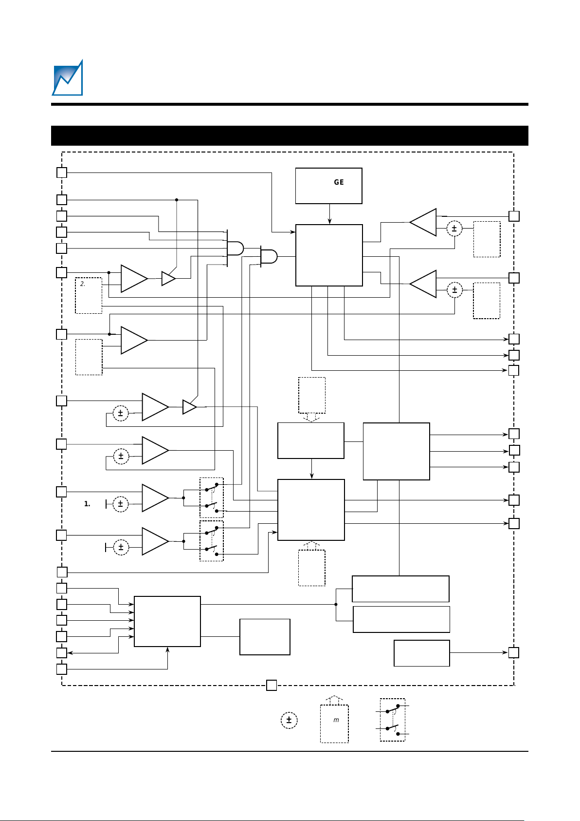
FUNCTIONAL BLOCK DIAGRAM
A0
A1
A2
SCL
SDA
PWR_EN
+
–
VCC
HST_3V_MON
+
–
CARD_3V_MON
CARD_5V_MON
LOCAL_PCI_RST
LOCAL_PCI_RST#
ISLEW
SGNL_VLD#
HEALTHY#
DRVREN#
FAULT#
VGATE5
VGATE3
1VREF
GND
BD_SEL2#
BD_SEL1#
±
±
2.65V
2.80V
2.95V
3.10V
4.625V
4.375V
+
–
+
–
PCI_RST#
+
–
MONITOR1
MONITOR 2
±
±
+
–
1.25V
1.25V
VSEL
RESET
CONTROLLER
25ms
50ms
100ms
200ms
3.2s
1.6s
0.8s
Off
WATCHDOG
TIMER
CS#
I2C
INTERFACE
+
–
CBI_3
CBI_5
+
–
25mV
50mV
75mV
125mV
25mV
50mV
75mV
125mV
±
±
CHARGE
PUMP
SLEW
RATE
CONTROLLER
CONTROL REGISTER
STATUS REGISTER
4K E
2
PROM
16
15
4
33
30
21
40
6
7
11
12
27
26
32
29
8
20
19
45
1
2
34
41
36
44
46
3
18
42
35
BANDGAP
CONTROL
LOGIC
2057 BD
±
25ms
50ms
100ms
200ms
Programmable Functions

5
2057 1.x 8/16/01
SMH4044
SUMMIT MICROELECTRONICS, Inc.
Preliminary
PIN CONFIGURATION
PIN DESCRIPTIONS
A0, A1, A2 (7, 11, 12)
Address inputs 0, 1 and 2 are used to set the three-bit
device address of the memory array. The state of these
inputs will determine the device address for the memory
if it is on a two-wire bus with multiple memories with the
same device type identifier.
SCL (27)
The SCL input is used to clock data into and out of the
memory array. In the write mode, data must remain stable
while SCL is HIGH. In the read mode, data is clocked out
on the falling edge of SCL.
SDA (26)
The SDA pin is a bidirectional pin used to transfer data into
and out of the SMH4044. Data changing from one state
to the other may occur only when SCL is LOW, except
when generating START or STOP conditions. SDA is an
open-drain output and may be wire-ORed with any number of open-drain outputs.
CARD_3V_MON (33)
This input monitors the card-side 3.3V supply. If the input
falls below V
TRIP
then the HEALTHY# and SGNL_VLD#
outputs are de-asserted and the reset outputs are driven
active.
CARD_5V_MON (40)
This input monitors the card-side 5V supply. If the input
falls below V
TRIP
then the HEALTHY# and SGNL_VLD#
outputs are de-asserted and the reset outputs are driven
active.
CBI_3 (36)
CBI_3 is the circuit breaker input for the low supply. With
a series resistor placed in the supply path between
HST_3V_MON and CBI_3, the circuit breaker will trip
whenever the voltage across the resistor exceeds 50mV.
FAULT#
1VREF
VSEL
PWR_EN
nc
MONITOR 1
A0
LOCAL_PCI_RST#
nc
nc
A1
A2
CBI_3
HST_3V_MON
VGATE3
CARD_3V_MON
CS#
nc
MONITOR 2
LOCAL_PCI_RST
nc
SCL
SDA
nc
nc
nc
BD_SEL2#
BD_SEL1#
nc
GND
HEALTHY#
SGNL_VLD#
PCI_RST#
ncncnc
nc
nc
ISLEW
DRVREN#
CBI_5ncVCC
VGATE5
CARD_5V_MON
ncncnc
1
2
3
4
5
6
7
8
9
10
11
12
1314151617181920212223
24
36
35
34
33
32
31
30
29
28
27
26
25
4847464544434241403938
37
2057 PCon

6
SMH4044
2057 1.x 8/16/01
SUMMIT MICROELECTRONICS, Inc.
Preliminary
CBI_5 (44)
CBI_5 is the circuit breaker input for the supply voltage.
With a series resistor placed in the supply path between
the 5V early power and CBI_5, the circuit breaker will trip
whenever the voltage across the resistor exceeds 50mV.
HST_3V_MON (35)
This input monitors the host 3.3V supply and it is used as
a reference for the circuit breaker comparator. If VCC3
falls below V
TRIP
then SGNL_VLD# is de-asserted, the
high side drivers are disabled, and LOCAL_PCI_RST# is
asserted.
ISLEW (46)
A Diode-connected NFET input. It may be used to adjust
the 250V/s default slew rate of the high-side driver
outputs.
PCI_RST# (21)
A TTL level reset input signal from the host interface. A
high to low transition (held low longer than 40ns) will
initiate a reset sequence. The LOCAL_PCI_RST# and
LOCAL_PCI_RST outputs will be driven active for a
minimum period of t
PURST
. If the PCI_RST# input is still
held low after t
PURST
times out the reset outputs will
continue to be driven until PCI_RST# is released.
PWR_EN (4)
A TTL level input that allows the host to enable or disable
the power to the individual card. During initial power up
this signal would start in a low state, and then be driven
high during software initialization. If this signal is driven
low then the power supply control outputs will be driven
into the inactive state and the reset signals asserted. In
a non-High Availability system this input can be tied high.
The PWR_EN input is also used to reset the SMH4044
circuit breakers. After an over-current condition is
detected the VGATE outputs can be turned back on by
first taking PWR_EN low then returning it high.
VSEL (3)
A TTL level input used to determine which of the host
power supply inputs will be monitored for valid voltage and
reset generation. This is a static input and the pin should
be tied to VCC or ground through a resistor. VSEL is high
for 3.3V power, and low for 5V or mixed mode power.
V
CC
(42)
The power supply input. It is monitored for power integrity.
If it falls below the 5V sense threshold (V
TRIP
) and the
VSEL input is low then the SGNL_VLD# and HEALTHY#
signals are de-asserted, the high side drivers disabled,
and reset outputs asserted. On a CompactPCI board this
must be connected to early power.
GND (18)
Power supply return line. Ground should be applied at the
same time as early power.
BD_SEL1#, BD_SEL2# (16, 15)
These are active low TTL level inputs with internal pullups to V
CC
. When pulled low they indicate full board
insertion. On the host side the signals should be directly
tied to ground. In a High Availability application these
inputs can be the last pins to mate with the backplane.
Alternatively, they can be actively driven by the host, or
be connected to switches interfaced to the board ejectors,
or any combination. Both inputs must be low before the
SMH4044 will begin to turn on the card side voltage.
DRVREN# (45)
An open-drain, active-low output that indicates the status
of the 3V and 5V high side driver outputs (VGATE5 and
VGATE3). This signal may also be used as a switching
signal for the 12V supply.
FAULT# (1)
An open-drain, active-low output. It will be driven low
whenever an over-current condition is detected. It will be
reset when the PWR_EN signal is brought low.
HEALTHY# (19)
An open-drain, active-low output indicating card side
power inputs are above their reset trip levels.
LOCAL_PCI_RST# (8)
An open-drain active-low output. It is used to reset the
card side circuitry on the add-in card. It is active
whenever the card-side monitor inputs are below their
respective V
TRIP
levels. It may also be driven low by a low
input on the PCI_RST# pin.
 Loading...