

Page 1
White LED driver for mid-size LCD display backlight
Features
■ Boost DC-DC converter
■ Drives up to 40 LEDs (4 strings of 10) with a
total current up to 120 mA
■ Input voltage range: 3.0 V to 21 V
■ Output current control
■ 1.4 MHz fixed frequency PWM control
■ PWM input for output current dimming with
frequency range 25 kHz - 50 kHz
■ 2 A integrated switch
■ Overvoltage protection
■ Chip overtemperature detection and protection
■ Less than 1 µA standby current
■ Soft-start function
■ Package DFN8 (3 x 3) 0.65 mm pitch
STLD41
Datasheet − production data
DFN8 (3 x 3 mm)
signal connected to the EN pin. The LEDs can be
dimmed by applying a PWM signal to the PWM
pin.
Applications
■ Mini PCs
■ PMP & PND
■ Printers
■ Game consoles
Description
The STLD41 is a boost converter that operates
from 3.0 V to 21 V and can provide an output
voltage as high as 38 V. It can drive up to 40 white
LEDs connected in 4 strings of 10 LEDs in series.
The total output current capability is 120 mA at an
output voltage of 38 V. Regulation is performed by
the internal error amplifier which works with the
feedback voltage from the sensing resistor. The
device can be turned ON/OFF by way of the logic
Table 1. Device summary
Order code Package Packaging
STLD41PUR DFN8 (3 x 3 mm) 3000 parts per reel
June 2012 Doc ID 022283 Rev 5 1/19
This is information on a product in full production.
www.st.com
19
Page 2

Contents STLD41
Contents
1 Block diagram . . . . . . . . . . . . . . . . . . . . . . . . . . . . . . . . . . . . . . . . . . . . . . 3
2 Pin configuration . . . . . . . . . . . . . . . . . . . . . . . . . . . . . . . . . . . . . . . . . . . . 4
3 Maximum ratings . . . . . . . . . . . . . . . . . . . . . . . . . . . . . . . . . . . . . . . . . . . . 5
4 Typical application circuit . . . . . . . . . . . . . . . . . . . . . . . . . . . . . . . . . . . . 6
5 Electrical characteristics . . . . . . . . . . . . . . . . . . . . . . . . . . . . . . . . . . . . . 7
6 Introduction . . . . . . . . . . . . . . . . . . . . . . . . . . . . . . . . . . . . . . . . . . . . . . . . 8
6.1 PWM input . . . . . . . . . . . . . . . . . . . . . . . . . . . . . . . . . . . . . . . . . . . . . . . . . 8
7 Selection of external components . . . . . . . . . . . . . . . . . . . . . . . . . . . . . . 9
7.1 CIN selection . . . . . . . . . . . . . . . . . . . . . . . . . . . . . . . . . . . . . . . . . . . . . . . . 9
7.2 C
7.3 Inductor selection . . . . . . . . . . . . . . . . . . . . . . . . . . . . . . . . . . . . . . . . . . . . 9
7.4 R
7.5 PCB layout . . . . . . . . . . . . . . . . . . . . . . . . . . . . . . . . . . . . . . . . . . . . . . . . 10
selection . . . . . . . . . . . . . . . . . . . . . . . . . . . . . . . . . . . . . . . . . . . . . . 9
OUT
value . . . . . . . . . . . . . . . . . . . . . . . . . . . . . . . . . . . . . . . . . . . . . . 10
SENSE
8 Typical performance characteristics . . . . . . . . . . . . . . . . . . . . . . . . . . . 13
9 Package mechanical data . . . . . . . . . . . . . . . . . . . . . . . . . . . . . . . . . . . . 14
10 Revision history . . . . . . . . . . . . . . . . . . . . . . . . . . . . . . . . . . . . . . . . . . . 18
2/19 Doc ID 022283 Rev 5
Page 3
STLD41 Block diagram
1 Block diagram
Figure 1. STLD41 block diagram
VIN
VLX
BIAS
20 V / 5 V
CONV
REFERENCE
PWM-V
CONV.
LOGIC
REF1
REF2
OVP
SOFT-START
PGND
STEP-UP
CONTROL
REF2
REF1
GND
FB
AM07829v1
Doc ID 022283 Rev 5 3/19
Page 4
Pin configuration STLD41
2 Pin configuration
Figure 2. Pin connections (top view)
Table 2 .
Exposed pad PGND Power ground
Pin description
Pin n° Symbol Description
1 GND Ground
2 FB Feedback connection
3 GND Analog ground
4 PGND Power ground
5 VLX Inductor connection
6 EN Enable input
7 VIN Supply voltage
8 PWM_IN PWM input for the output current dimming
4/19 Doc ID 022283 Rev 5
Page 5
STLD41 Maximum ratings
3 Maximum ratings
Table 3. Absolute maximum ratings
Symbol Parameter Value Unit
VIN Signal supply voltage - 0.3 to 23 V
VLX Inductor connection - 0.3 to 40 V
FB Feedback connection - 0.3 to 2 V
EN Logic pin - 0.3 to 21 V
PWM_IN PWM input - 0.3 to 6 V
ESD Human body model ± 2kV
P
TOT
T
OP
T
J
T
STG
1. Power dissipation is dependent on the PCB. PCB design recommendations are included in
Continuous power dissipation (at TA = 70 °C)
Operating ambient temperature range - 40 to 85 °C
Junction temperature - 40 to 150 °C
Storage temperature range - 65 to 150 °C
(1)
TBD mW
Section 7.5: PCB layout
.
Note: Absolute maximum ratings are those values beyond which damage to the device may occur.
Functional operation under these conditions is not implied.
Table 4. Thermal data
Symbol Parameter Value Unit
R
thJA
Thermal resistance junction-ambient 46 °C/W
Doc ID 022283 Rev 5 5/19
Page 6
Typical application circuit STLD41
4 Typical application circuit
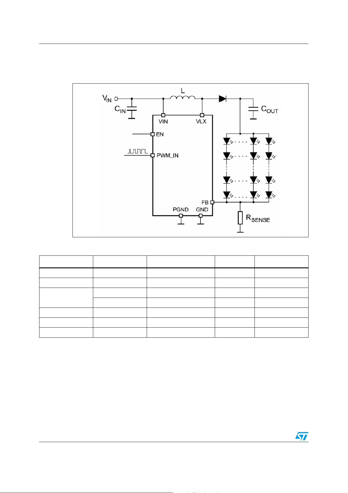
Figure 3. Application circuit schematic
Table 5. List of external components
Component Manufacturer Part number Value Size
C
IN
C
OUT
L
R
SENSE
Schottky diode STMicroelectronics STPS1L40M 1 A / 40 V 3.75 x 1 x 1.9 mm
LED OSRAM LWL283-Q1R2-3K8L-1-Z 20 mA / 3.1 V 0603
Murata GRM32ER71H106K 10 µF / 50 V 3.2 x 2.5 x 2.5 mm
Murata GRM31CR61H225KA88L 2.2 µF / 50 V 3.2 x 1.6 x 1.6 mm
Murata LQH6PPN470M43 47 µH / 1.25 A 6 x 6 x 4.3 mm
Coilcraft LPS6235-473MLB 47 µH / 1.2 A 6 x 6 x 3.5 mm
Tyco Electronics 1.3 Ω 0603 size
Note: The above listed components refer to a typical application with a maximum performance
setting. Operation of the STLD41 is not limited to the choice of these external components.
6/19 Doc ID 022283 Rev 5
Page 7
STLD41 Electrical characteristics
5 Electrical characteristics
C
= 10 µF, C
IN
Values are at 25 °C, unless otherwise specified.
Table 6. Electrical characteristics
Symbol Parameter Test conditions Min. Typ. Max. Unit
= 2.2 µF, L = 47 µH / 1.25 A, R
OUT
= 1.3 Ω, TA = 25 °C, V
SENSE
= 5.5 V typ.
IN
V
V
I
PEAK
ΔI
V
V
FBMIN
OVP
Input operating supply
IN
voltage
Output current
I
O
adjustment range
Regulated voltage range V
OUT
Inductor peak current VIN = 3 V, V
Output current variation V
O
Quiescent current in
I
Q
Standby mode
Feedback voltage I
FB
= 3.0 V to 5.0 V; V
V
IN
= 5.0 V to 7.0 V; V
IN
V
= 7.0 V to 18 V; V
IN
= 3.0 V to 21 V 1.15*V
IN
= 38 V 2 A
OUT
= 3 V, I
IN
EN = LOW, V
= 120 mA, PWM_IN=HIGH 144 160 176 mV
LED
= 120 mA -10 10 %
LED
= 5.5 V 1 µA
IN
= 38 V 40
OUT
= 38 V 78
OUT
= 38 V 120
OUT
3.0 21 V
IN
Min. feedback voltage PWM_IN = 30 kHz, duty cycle = 10% 35 mV
f
Frequency V
s
Efficiency of the chip itself
ν
(1)
Efficiency of the whole
ν
application
(2)
Output overvoltage
protection
= 3.0 V 1.4 MHz
IN
V
= 7 to 21 V, IO = 120 mA,
IN
= 10 x V
V
O
V
= 3 to 21 V, IO = 78 mA 79 %
IN
V
= 21 V, No load 40 V
IN
FLED_max+VRSENSE
= 38 V
87 %
mAV
38 V
OTP
OT
V
I
ENHIGH
T
f
PWM
V
1. Calculated as (V
2. Calculated as (V
Overtemperature
protection
Overtemperature
HYST
hysteresis
V
IL
Low and high level input
logic signal on EN pin
IH
Enable input current V
LED current rise time I
ON
= 0 to I
PWM dimming signal
frequency
PWM signal level V
PWM
= max
LED
OUT*ILED
LED*ILED
LED
)/(VIN*IIN), guaranteed by design
)/(VIN*IIN), guaranteed by design
= 21 V 140 °C
V
IN
= 21 V 20 °C
V
IN
00.4
V
= 3.0 V to 21 V
IN
= 3.0 V to 21 V, V
IN
V
= 10 V 1 ms
IN
= 3.0 V to 21 V 25 50 kHz
V
IN
= 3.0 V to 21 V 1.4 5.5 V
IN
= 21 V 10 µA
EN
1.4 V
I
Doc ID 022283 Rev 5 7/19
V
Page 8

Introduction STLD41
6 Introduction
The STLD41 is a boost converter, dedicated to power and control the current of white LEDs
in an LCD backlight. The device operates at a typical constant switching frequency of 1.4
MHz. It steps an input voltage ranging from 3.0 V to 21 V up to 40 V. The output current is
dimmable by the PWM signal applied to the PWM pin.
6.1 PWM input
The light intensity can be dimmed by a signal applied to the PWM input. It is recommended
to use a signal whose frequency is between 25 kHz to 50 kHz. The maximum amplitude of
the signal is limited to 5.5 V. The minimum level of the signal must be at least 1.4 V. The
dimming range is from 20% to 100% of the current set by the R
SENSE
.
8/19 Doc ID 022283 Rev 5
Page 9

STLD41 Selection of external components
()
7 Selection of external components
7.1 CIN selection
It is recommended to use 10 µF as the input capacitor to achieve good stability of the device
and low noise on the V
track.
IN
7.2 C
selection
OUT
It is recommended to use 2.2 µF as the optimal value of output capacitor to achieve the best
compromise between output voltage ripple and load transient response. The output ripple
can be checked using the equation for step-up architecture:
Equation 1
V
−
PKPK
7.3 Inductor selection
A thin shielded inductor with a low DC series winding resistance is recommended for this
application. To achieve good efficiency in step-up mode, it is recommended to use an
inductor with a DC series resistance R
resistance of the LED [Ω, Ω, 1].
For nominal operation, the peak inductor current can be calculated using this formula:
Equation 2
=
DCL
−∗
2
OUTOUT
= RD / 10 [Ω, Ω, 1], where RD is the dynamic
100*VVI
)MIN(INOUT)MAX(OUT
[]
∗∗
fVC
Hz,F,V,A;V
2
∗−
VVV
ININOUT
V
OUT
∗
2
V
IN
I
PEAK
I
OUT
=
()
+
n
∗∗∗
VfL2
OUT
where:
I
= Peak inductor current
PEAK
I
= Current sourced at the V
OUT
OUT
pin
n = Efficiency of the STLD41
V
= Output voltage at the V
OUT
V
= Input voltage at the VBAT-pin
IN
OUT
pin
L = Inductance value of the inductor
f = Switching frequency
For optimal performance of the STLD41 device, is recommended to use an inductor value of
47 µH or higher with low serial resistance and relevant saturation current calculated from the
equation above.
Doc ID 022283 Rev 5 9/19
Page 10

Selection of external components STLD41
7.4 R
R
SENSE
SENSE
value
= V
REF1
If using a typical setting of I
must be rated for a power dissipation of 1.3 x 0.12² W = 0.02 W.
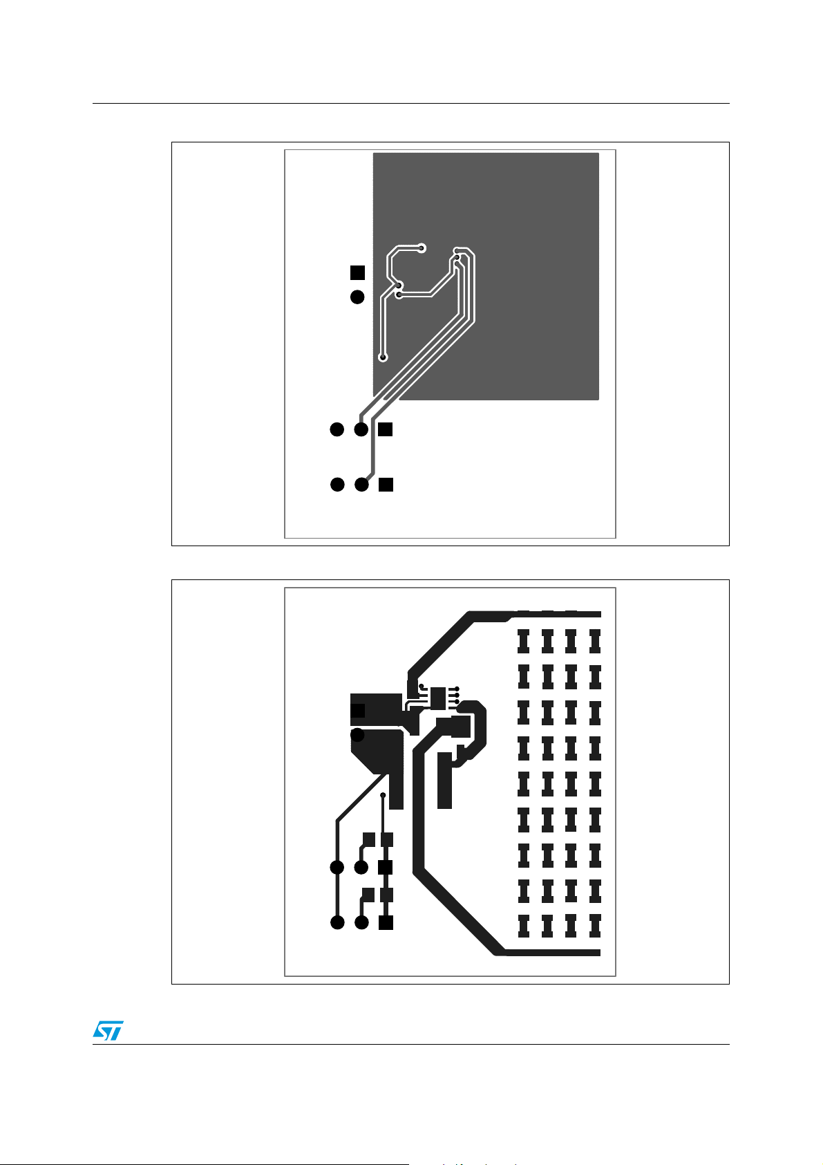
7.5 PCB layout
Because the STLD41 is a powerful switched device, the PCB must be designed in line with
rules for designing switched supplies. It is recommended to use a two-layer PCB. The power
wirings must be as short as possible and wide. Place all external components close to the
STLD41 device. High-energy switched loops should be as small as possible to reduce EMI.
Most LEDs need cooling, which can be attained utilizing a defined copper area on the PCB.
Use the reference guide for each LED to design the heatsink. Place the R
close as possible to pin 2 and ground of the system. The ground of the system is
represented by the size of the area created by the connections GND-PGDN-GND
GND
PCB must be focused on the minimum area of the application ground; the smaller the
ground area of the DC-DC converter
issues. It is recommended to place the copper plate connected through the vias to the
exposed pad to the bottom layer to create the heatsink of the device.
. When a change of PCB layer is needed, use sufficient vias. During routing, the
COUT
/ I
LED
= 120 mA, V
LED
= 160 mV, and R
REF1
(a)
, the better the stability and there will be fewer noise
= 1.3 Ω, the resistor
SENSE
SENSE
resistor as
-
CIN
a. The application ground area is represented by the area which is created by the ground pins of the CIN, C
and ground of the DEVICE and GND connection of the load.
10/19 Doc ID 022283 Rev 5
OUT
,
Page 11
STLD41 Selection of external components
Figure 4. Top layer
Figure 5. Bottom layer
Doc ID 022283 Rev 5 11/19
Page 12

Selection of external components STLD41
Figure 6. Top overlay
12/19 Doc ID 022283 Rev 5
Page 13

STLD41 Typical performance characteristics
8 Typical performance characteristics
Figure 7. Eff. vs. VIN, 6 x 6 LEDs, V
= 24 V Figure 8. Eff. vs. VIN, 5 x 7 LEDs, V
OUT
100
95
90
85
80
75
Eff [%]
70
65
60
55
I
I
I
OUT
OUT
OUT
=120m
=81mA
=66mA
I
I
OUT
OUT
=51mA
=35mA
I
=25mA
OUT
I
=15mA
OUT
50
5678 9 10111213 14 15 16 17 18 19 20 21 22
V
[V]
IN
Figure 9. Eff. vs. VIN, matrix 4 x 9 LEDs,
V
= 33 V
I
OUT
I
OUT
I
OUT
OUT
=120mA
=81mA
=66mA
I
I
OUT
OUT
=51mA
=35mA
V
IN
I
=25mA
OUT
I
=15mA
OUT
[V]
100
95
90
85
80
75
Eff [%]
70
65
60
55
50
5678 9 10111213 14 15 16 17 18 19 20 21 22
100
95
90
85
80
75
Eff [%]
70
65
60
55
50
Figure 10. Application eff. vs. V
I
=120mA
OUT
I
=81mA
OUT
I
=66mA
OUT
5678 910111213 14 15 16 17 18 19 20 21 22
I
I
OUT
OUT
=51mA
=35mA
V
I
=25mA
OUT
I
=15mA
OUT
[V]
IN
, matrix 4 x
IN
10 LEDs
I
=120mA
OUT
I
=78mA
OUT
95
90
85
80
75
Eff [%]
70
65
60
55
50
2 3 456 78 910111213 14 15 16 17 18 19 20 21 22
I
=25mA
OUT
IIN@120mA
[V]
V
IN
IIN@78mA
IIN@25mA
OUT
= 27 V
1200
1000
800
600
400
200
0
[mA]
IN
I
Figure 11. Output current regulation at 4 x 10
140
130
120
110
100
90
80
[mA]
70
OUT
I
60
50
40
30
20
10
LEDs
120mA / Rsens e=1R3
100mA / Rsens e=1R6
50mA / Rsens e=3R3
20mA / Rsens e=8R2
2 3 45678 910111213 14 15 16 17 18 19 20 21 22
V
[V]
IN
Doc ID 022283 Rev 5 13/19
Figure 12. VFB vs. PWM 25 kHz, V
I
OUTset
180
170
160
150
140
130
120
110
100
[mV]
90
FB
80
V
70
60
50
40
30
20
10
0102030405060708090100
= 120 mA
DC [%]
= 5.5 V,
IN
Page 14

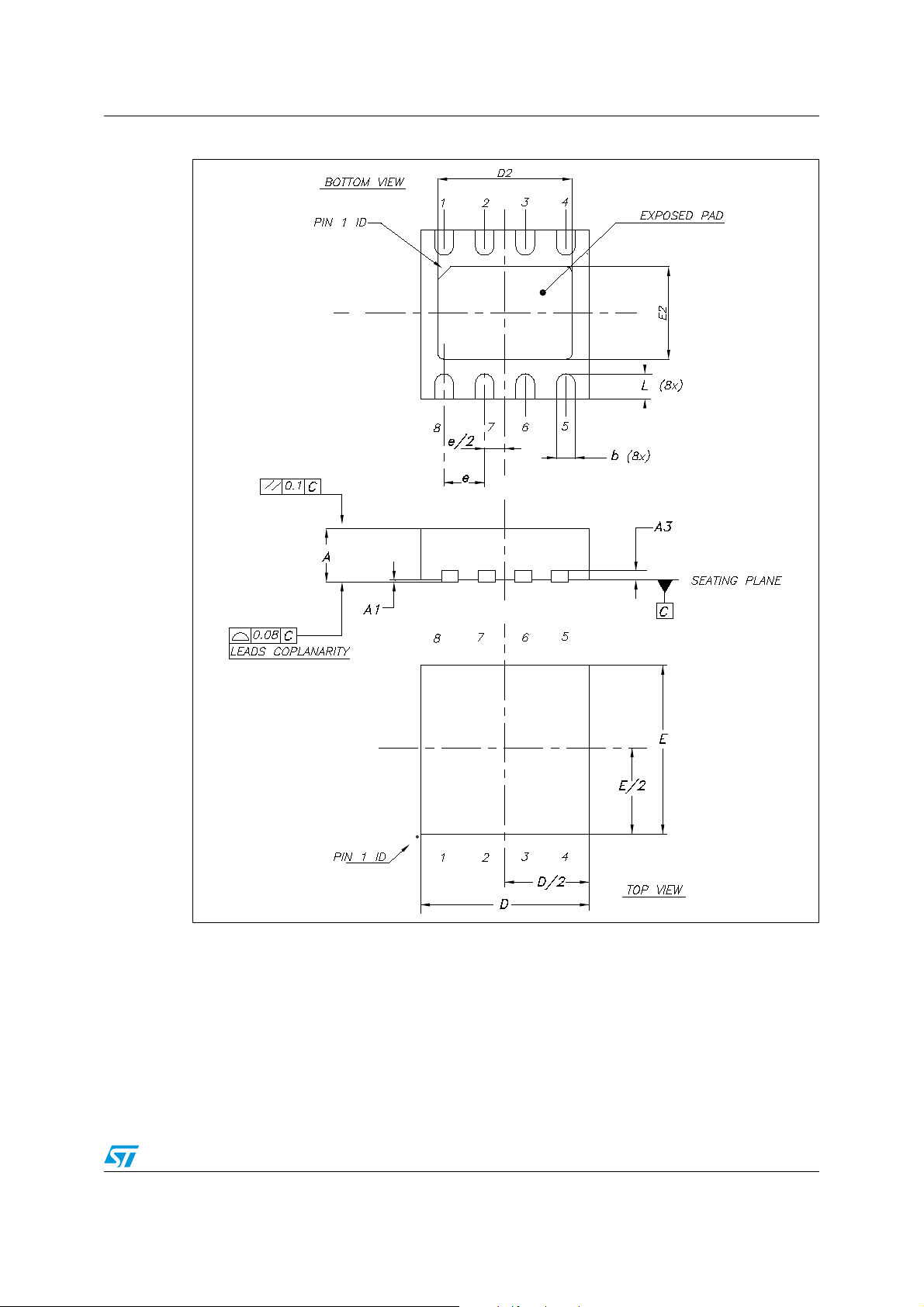
Package mechanical data STLD41
9 Package mechanical data
In order to meet environmental requirements, ST offers these devices in different grades of
®
ECOPACK
specifications, grade definitions and product status are available at:
ECOPACK
packages, depending on their level of environmental compliance. ECOPACK®
®
is an ST trademark.
www.st.com
.
Table 7. DFN8 (3 x 3 mm) mechanical data
mm.
Dim.
Min. Typ. Max.
A 0.80 0.90 1.00
A1 0.00 0.02 0.05
b 0.25 0.30 0.35
D3.00
D2 2.234 2.384 2.484
E3.00
E2 1.496 1.646 1.746
e0.65
L 0.30 0.40 0.50
14/19 Doc ID 022283 Rev 5
Page 15
STLD41 Package mechanical data
Figure 13. Package dimension DFN8 (3 x 3 mm)
8057023/B
Doc ID 022283 Rev 5 15/19
Page 16
Package mechanical data STLD41
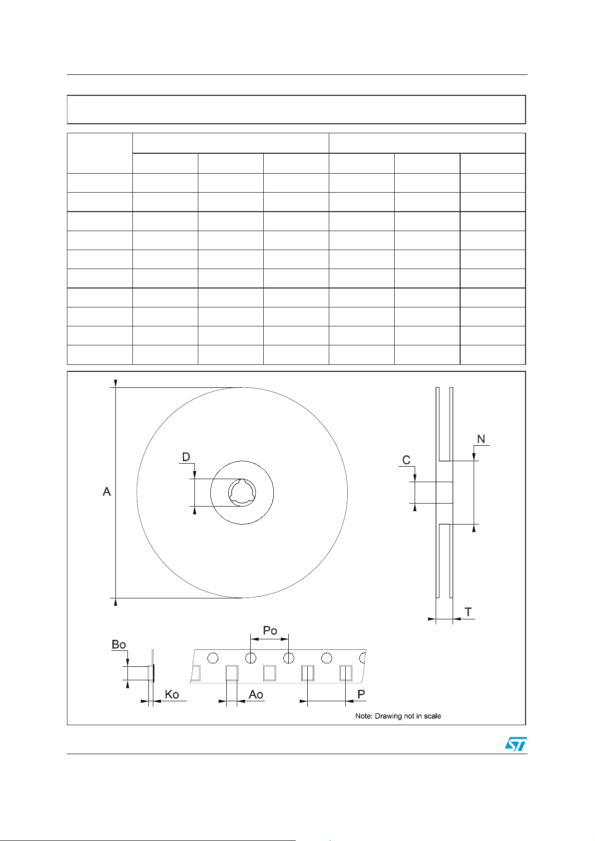
Tape & reel QFNxx/DFNxx (3x3) mechanical data
mm. inch.
Dim.
Min. Typ. Max. Min. Typ. Max.
A180 7.087
C 12.8 13.2 0.504 0.519
D 20.2 0.795
N60 2.362
T 14.4 0.567
Ao 3.3 0.130
Bo 3.3 0.130
Ko 1.1 0.043
Po 4 0.157
P 8 0.315
16/19 Doc ID 022283 Rev 5
Page 17
STLD41 Package mechanical data
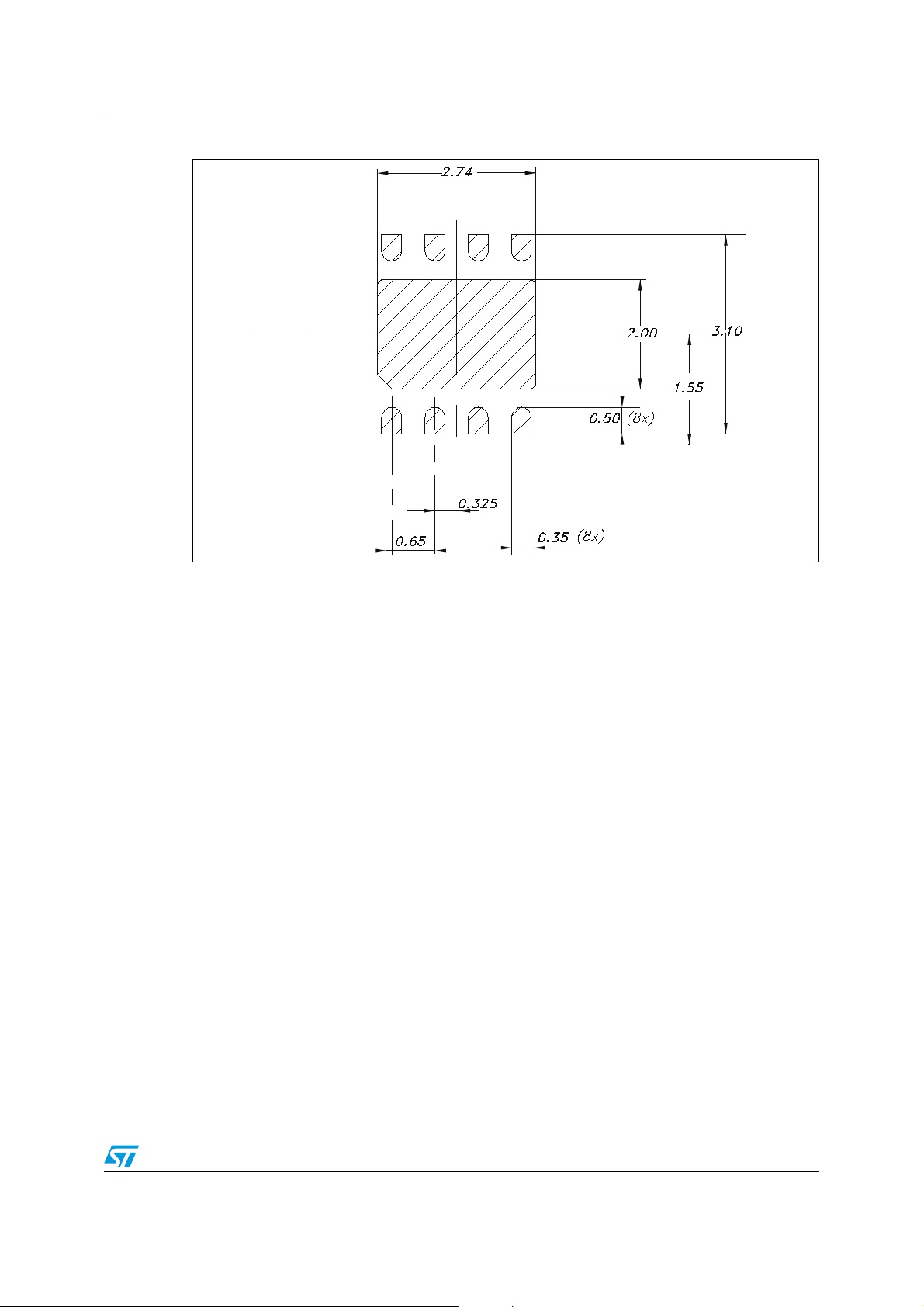
Figure 14. DFN8 (3 x 3) footprint recommended data (mm.)
Doc ID 022283 Rev 5 17/19
Page 18
Revision history STLD41
10 Revision history
Table 8. Document revision history
Date Revision Changes
28-Sep-2011 1 Initial release.
16-Nov-2011 2 Change value 1.8 MHz ==> 1.4 MHz
15-Mar-2012 3 Modified: 1.3 x 0.122 W ==> 1.3 x 0.12²
23-May-2012 4 Document status promoted from preliminary data to production data.
27-Jun-2012 5 Added: new L component Coilcraft
: Features on page 1
W
Section 7.4 on page 10
Table 5 on page 6
.
.
.
18/19 Doc ID 022283 Rev 5
Page 19

STLD41
Please Read Carefully:
Information in this document is provided solely in connection with ST products. STMicroelectronics NV and its subsidiaries (“ST”) reserve the
right to make changes, corrections, modifications or improvements, to this document, and the products and services described herein at any
time, without notice.
All ST products are sold pursuant to ST’s terms and conditions of sale.
Purchasers are solely responsible for the choice, selection and use of the ST products and services described herein, and ST assumes no
liability whatsoever relating to the choice, selection or use of the ST products and services described herein.
No license, express or implied, by estoppel or otherwise, to any intellectual property rights is granted under this document. If any part of this
document refers to any third party products or services it shall not be deemed a license grant by ST for the use of such third party products
or services, or any intellectual property contained therein or considered as a warranty covering the use in any manner whatsoever of such
third party products or services or any intellectual property contained therein.
UNLESS OTHERWISE SET FORTH IN ST’S TERMS AND CONDITIONS OF SALE ST DISCLAIMS ANY EXPRESS OR IMPLIED
WARRANTY WITH RESPECT TO THE USE AND/OR SALE OF ST PRODUCTS INCLUDING WITHOUT LIMITATION IMPLIED
WARRANTIES OF MERCHANTABILITY, FITNESS FOR A PARTICULAR PURPOSE (AND THEIR EQUIVALENTS UNDER THE LAWS
OF ANY JURISDICTION), OR INFRINGEMENT OF ANY PATENT, COPYRIGHT OR OTHER INTELLECTUAL PROPERTY RIGHT.
UNLESS EXPRESSLY APPROVED IN WRITING BY TWO AUTHORIZED ST REPRESENTATIVES, ST PRODUCTS ARE NOT
RECOMMENDED, AUTHORIZED OR WARRANTED FOR USE IN MILITARY, AIR CRAFT, SPACE, LIFE SAVING, OR LIFE SUSTAINING
APPLICATIONS, NOR IN PRODUCTS OR SYSTEMS WHERE FAILURE OR MALFUNCTION MAY RESULT IN PERSONAL INJURY,
DEATH, OR SEVERE PROPERTY OR ENVIRONMENTAL DAMAGE. ST PRODUCTS WHICH ARE NOT SPECIFIED AS "AUTOMOTIVE
GRADE" MAY ONLY BE USED IN AUTOMOTIVE APPLICATIONS AT USER’S OWN RISK.
Resale of ST products with provisions different from the statements and/or technical features set forth in this document shall immediately void
any warranty granted by ST for the ST product or service described herein and shall not create or extend in any manner whatsoever, any
liability of ST.
ST and the ST logo are trademarks or registered trademarks of ST in various countries.
Information in this document supersedes and replaces all information previously supplied.
The ST logo is a registered trademark of STMicroelectronics. All other names are the property of their respective owners.
© 2012 STMicroelectronics - All rights reserved
STMicroelectronics group of companies
Australia - Belgium - Brazil - Canada - China - Czech Republic - Finland - France - Germany - Hong Kong - India - Israel - Italy - Japan -
Malaysia - Malta - Morocco - Philippines - Singapore - Spain - Sweden - Switzerland - United Kingdom - United States of America
www.st.com
Doc ID 022283 Rev 5 19/19
Page 20

 Loading...