

Page 1

THERMAL PRINTER
TUP400 Series
TECHNICAL MANUAL
[ SECOND EDITION ]
Page 2

NOTICE
• All rights reserved. Reproduction of any part of this manual in any form whatsoever, without
STAR’s express permission is forbidden.
• The contents of this manual are subject to change without notice.
• All efforts have been made to ensure the accuracy of the contents of this manual at the time of going
to press. However, should any errors be detected, STAR would greatly appreciate being informed
of them.
• The above notwithstanding, STAR can assume no responsibility for any errors in this manual.
© Copyright 1997 Star Micronics Co.,Ltd.
Page 3
• First edition : Aug.1997
• Second edition : Jun. 1998 Add interface board Ver. 2
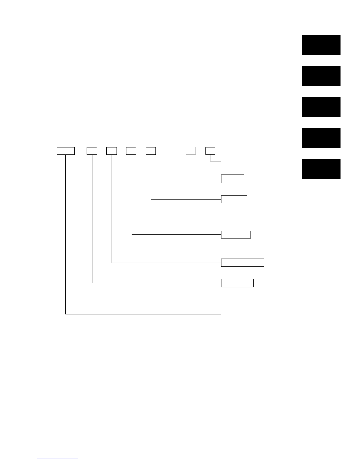
Model Name
TUP 4 5 2 V2 D — 24 NL
No Transparent Laser
Voltage
24 : 24 VDC
Interface
D: RS232C
C: Parallel
K: RS422A
Board type
None:Ver.1
V2:Ver.2
Mechanism type
2: 40 columns
Printer type
5: Guilotine Type Full Cutter
8: Guillotine Type Full Cutter + Presenter
TUP400-series thermal printer
INTRODUCTION
This manual was created as a reference for maintenance of the Thermal Printer TUP400 Series for
personnel who are responsible for periodic inspections or troubleshooting of that equipment. This manual
was written for maintenance personnel, and was not intended to be used by the general operator.
This manual is organized into the following chapters.
Chapter 1 Specifications and Operation
Chapter 2 Theory of Operation
Chapter 3 Parts Replacement and Related Adjustments
Chapter 4 Maintenance and Lubrication
Chapter 5 Parts Lists
1
5
4
3
2
Page 4

This page was intentionally left blank.
Page 5

CHAPTER 1
SPECIFICATIONS AND OPERATION
1. General Specifications ....................................................................................... 6
2. External Appearance .......................................................................................... 7
3. DIP-Switch Settings ............................................................................................8
4. Print-Density Adjustment ................................................................................. 11
5. Sensor Adjustment ...........................................................................................12
6. HEX Dump Mode/Test Print.............................................................................. 13
7. Changing the Interface Board..........................................................................14
1
Page 6
– 6 –
1. General Specifications
Printing method Line thermal direct
Resolution 8 dots/mm (H) × 8 dots/mm (V)
Printable width 50 mm in Line Mode; 80 mm in Page Mode
Printing speeds 2 Inches/sec and 1 Inch/sec
Printable characters Page mode: ANK, International, Slash zero
Line mode: ANK, International, Special, Block graphics, IBM special,
IBM block graphics, Chinese characters, Slash zero
NOTE: ANK is comprised of ASCII characters and Japanese katakana characters.
Character matrixes Page mode
Small 8×16
Standard 16×24
Wide 24×32
OCR-B 16×24
Chinese chara. 24×24
Line mode
IBM block graphic 12×24 or 12×32
Chinese chara. 24×24 (12×24)
All others 12×24
Bar Codes JAN, EAN, UPC, Code39, ITF, Code93, Code128, NW-7
Paper
Recommended brands TF50KS-E, TF62KS-E (Nippon Paper Industries)
KP50-HEAEX (New Oji Paper Co., Ltd.)
Width 82.5 mm(3.25 inches)
Thickness General thermal paper 60 to 85 µm
Roll diameters External 203 mm max. (8 Inch), Internal 32 mm (1.26 Inch)
Interface RS232C, RS422A, or Parallel
MCBF 5,000,000 Lines
Head longevity 100 Km or 1.0 x 10⁸ pulses(excludes damaged caused by dirt or foreign objects.)
(Missing dots is Max. 5%. However, there will be no missing dots up to 50Km.
This is the point where the thermal body resistor value varies more than 15% of the
initial value when continuously printing up to 12.5% of the printing rate.)
Cutter longevity 300,000 cuts (One piece max. paper thickness: 85 µm.)
Power supply DC 24 V ±7%
Power consumption Max. 120 W
Operating environment Temperature 5°C to 40°C
Humidity 25% to 80% (No condensation)
Storage environment Temperature -20°C to 60°C
Humidity 10% to 90% (No condensation)
Fig. 1-1 External Dimensions
164mm
164mm
299mm
254mm
356mm
Approximately 3.3kg
Approximately 3.1kg
254mm
TUP452
TUP482
0
-1
Page 7
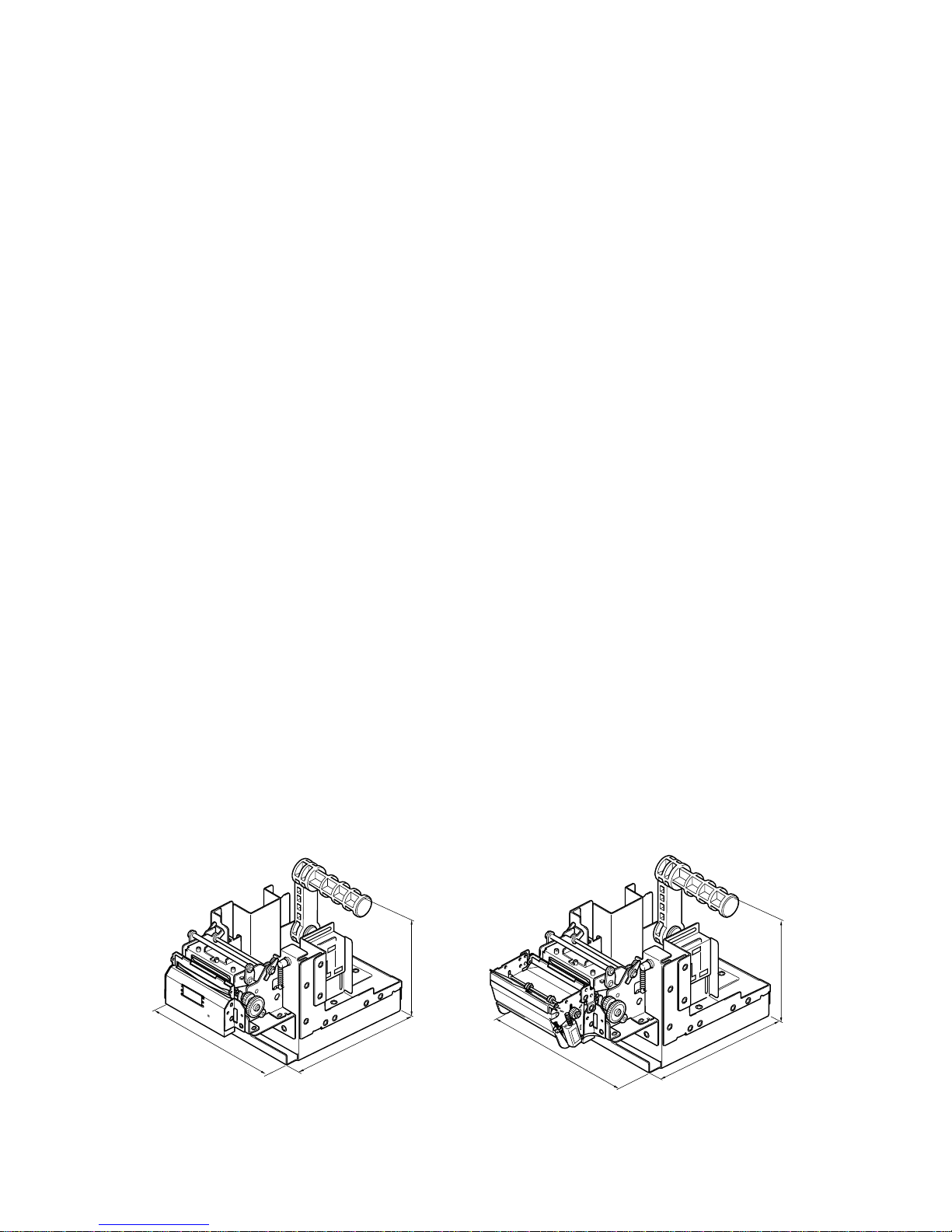
– 7 –
Fig. 1-2-b Internal Configuration (TUP482)
Arm
Printer head
Presenter
Fig. 1-2-a Internal Configuration (TUP452)
2. External Appearance
Printer head
Arm
Cutter
Page 8
– 8 –
3. DIP-Switch Settings
DIP switches are located on the interface board and they differ according to the type of interface.
(1) Setting the DIP Switches
1. Turn the power supply OFF.
2. Remove the screw holding the ROM cover in place. (The screw is located at the base of the paper-roll holder.)
3. Remove the ROM cover to expose the main and interface PCBs
4. Set the DIP-switches on the interface board.
Fig. 1-3 DIP-Switch Settings
DIP Switches
VP4 (Black Mark Sensor)
EPROM
Main Logic Board
VP3 (Paper End Sensor)
Interface Board (RS-232C)
Fig. 1-4 Main Interface Board
Page 9
– 9 –
2. DIP-switch values
(1) RS-232C interface
This board has a single 8-bit DIP switch.
Switch Setting ON OFF
1-1 Baud
1-2
1-3 Handshake DTR XON/XOFF
1-4 Data 8 bits 7 bits
1-5 Parity No parity Enabled
1-6 Parity Odd Even
1-7 DC1/DC3 Disabled Enabled
1-8 Power ON
Baud 1-1 1-2
2400BPS OFF OFF
4800BPS OFF ON
9600BPS ON ON
19200BPS ON OFF
Mode 1-8 ON Power On
DC1/DC3 Disabled Disabled Printer selected
DC1/DC3 Disabled ON Printer selected
OFF Printer de-selected
Addressable ON Printer de-selected
OFF Printer selected
*1 The old type is selected.
Page 10

– 10 –
(2) RS-422A interface
This board had two DIP switches: one 8-bit switch and one 4-bit switch.
DIP switch #1 (8 bits):
Identical to the DIP switch on the RS-232C. (Bit 1-7 is disabled.)
DIP switch #2 (4 bits):
SW2-1 SW2-2 SW3-3 SW2-4
DC1,3 off ON ON ON ON
Address #1 OFF ON ON ON
#2 ON OFF ON ON
#3 OFF OFF ON ON
#4 ON ON OFF ON
#5 OFF ON OFF ON
#6 ON OFF OFF ON
#7 OFF OFF OFF ON
#8 ON ON ON OFF
#9 OFF ON ON OFF
#10 ON OFF ON OFF
#11 OFF OFF ON OFF
#12 ON ON OFF OFF
#13 OFF ON OFF OFF
#14 ON OFF OFF OFF
DC1,3 mode on OFF OFF OFF OFF
* DIP-SW #2 overrides the DIP-SW #1 DC1/3 setting (bit 1-7).
* DIP-SW #2 factory setting: All ON
(3) Parallel (Centronics) interface
The parallel-interface board has no DIP switches.
Page 11
– 11 –
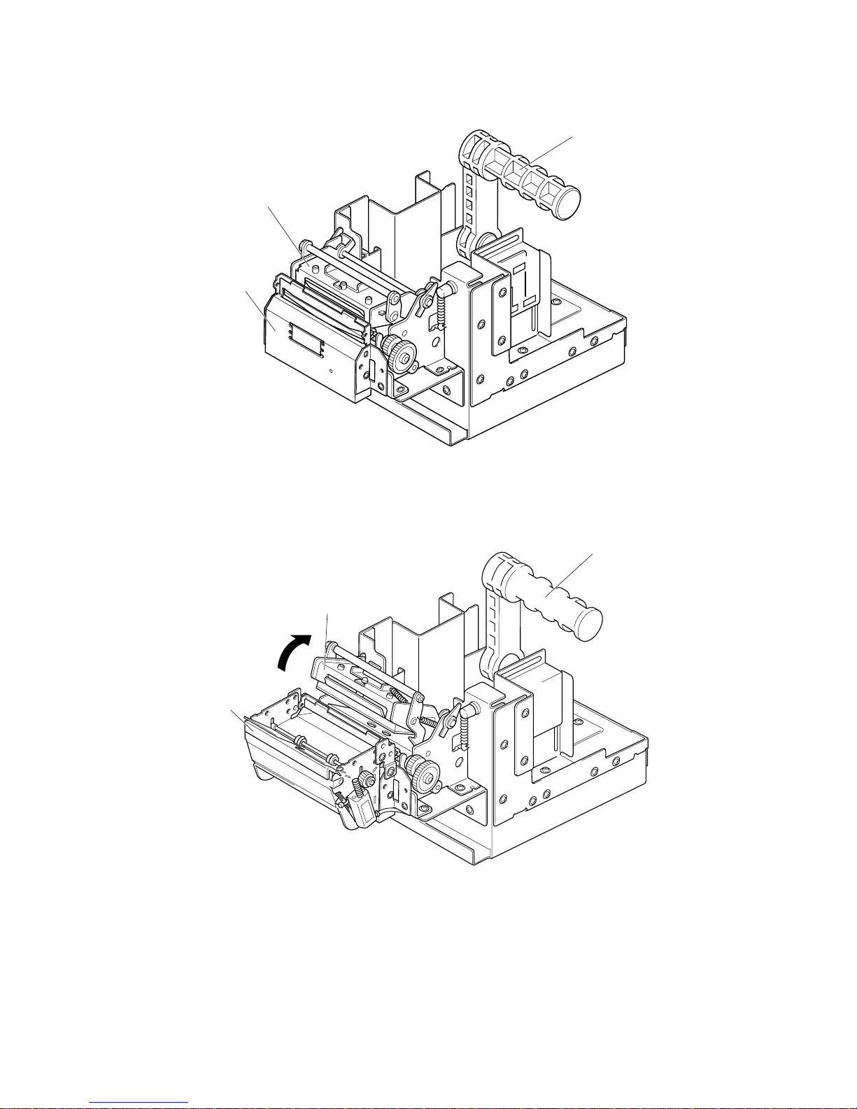
4. Print-Density Adjustment
Adjust the print density in accordance with the sensitivity of the paper being used.
Fig. 1-5 Print-Density Adjustment
1. The variable resistor is located to the left of the interface connector on the back side of the printer.
2. Use a phillips screw driver to rotate the variable resistor to adjust the print density. The variable resistor will
rotate approximately 180°.
If you are not getting a good print on the thermal paper with the density set to its maximum at 2 Inch/sec print
speed, set the print speed to 1 Inch sec.
CAUTION
Avoid setting density too high for sensitive paper types. Excessive dark values may cause the paper
to swell which will degrade the quality of the image.
Variable Resistor
Approx. 90
Light Dark
Approx. 90
Page 12

– 12 –
5. Sensor Adjustment
You must adjust the paper sensor for the paper quality and the black mark print.
Fig. 1-6 Sensor Adjustment
1) Remove the screw on the underside of the paper-roll holder and remove the ROM cover.
2) Turn ON the power supply while holding down the push switch on the Near-end Sensor Board.
Remove the push-switch within 3 seconds after the "HU" LED on the Near-end Sensor Board lights.
CAUTION
If you continue holding the push switch for more than 3 seconds, the "PE" LED will light and you will not
be able to make any adjustments.
3) Black Mark Sensor
• Insert a piece of paper into the mechanism’s sensor area. Set it anywhere but the book mark area.
• Rotate the variable resistor VR4 on the main logic board until the "HU" LED on the Near-end Board lights.
Paper End Sensor
• Insert a piece of paper into the mechanism’s sensor area. Set it anywhere but the book mark area.
• Rotate the variable resistor VR3 on the main logic board until the "PE" LED on the Near-end Board lights.
4) After the LED lights, press the RESUME switch.
VR4
EPROM
Main Logic Board
VR3
Interface Board
Page 13

– 13 –
6. HEX Dump Mode/Test Print
You can enter the HEX Dump Mode and run Test Prints by turning ON the power supply while pressing the RESUME
switch. The HEX Dump mode prints the data sent from the host computer in HEX data format.
1) Turn ON the power supply while pressing the RESUME switch.
2) Release the RESUME switch using the following timing to set each mode.
Releasing at a: HEX Dump Mode
Releasing at b: Test Print
2 Sec
a
b
HU Lights
PE Lights
Near-end Sensor Board LED
Page 14
– 14 –
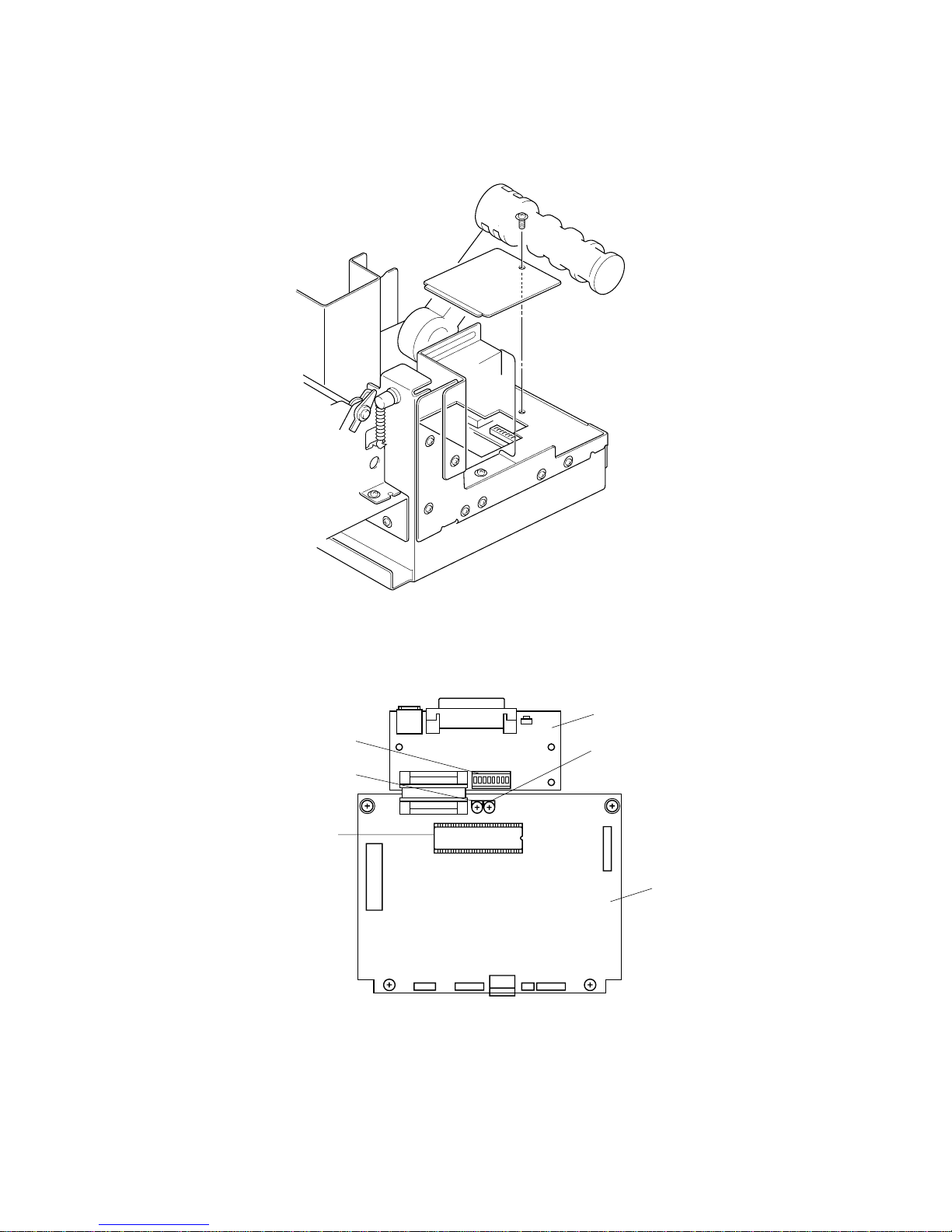
7. Changing the Interface Board
You can change the printer’s interface by replacing the interface board.
Fig. 1-7 Changing the Interface Board
1. Turn the power supply OFF.
2. Remove the 2 Interface Board Screws.
3. Remove the Interface Board.
4. Insert the new Interface Board by pushing it along the guides.
Push until the connector is completely inserted.
5. Attach the 2 screws to attach the Interface Board to the printer.
(Note)
The printer will automatically recognize the new Interface Board when it has been changed.
Page 15

CHAPTER 2
THEORY OF OPERATION
This chapter describes the operating principles of the circuitry and printer mechanism.
1. Block Diagram ................................................................................................... 16
2. Main Logic Board ..............................................................................................18
2-1. Data I/O Circuitry .................................................................................................. 18
2-1-2.RS-422A Interface............................................................................................ 19
2-1-3. Parallel Interface.......................................................................................... 20
2-2. Editing and Printing ............................................................................................. 21
2-2-1. Editing .......................................................................................................... 21
2-2-2. Thermal Head............................................................................................... 21
2-2-3. Head Current Control .................................................................................. 22
2-3. Feed-Motor Drive Circuit...................................................................................... 23
2-4. Power-On Reset Circuit ....................................................................................... 24
2-5. +5V Line Voltage Detector Circuit....................................................................... 25
3. Printer Mechanism ............................................................................................26
3-1. Thermal Head........................................................................................................ 26
3-2. Paper-Feed Mechanism ....................................................................................... 26
3-3. Sensor ................................................................................................................... 27
2
Page 16
– 16 –
1. Block Diagram
The following is the block diagram for this printer.
(16)
(16)
(8)
(8)
(16)
24V
Data (Host Computer)
Near-end
Sensor Board
RESUME
Switch
Main Logic Board
Gate Array
CPU
DC-DC Coverter
Power Supply Unit
EPROM
128 k x 16 Bit (Ver. 1
)
250 k x 16 Bit (Ver. 2
)
PS-RAM
128 x 16 BitPS-RAM
S-RAM
8K x 8 BitS-RAM
Chinese Char. ROM
256 k x 16 Bit (Ver. 1
)
512 k x 16 Bit (Ver. 2
)
EEPROM
Head Driver
Motor Driver
Cutter Driver
Sensor Circuit
Presenter
Driver
Thermal
Head
Print Mechanism
Paper
Feed
Motor
Cutter
Sensor
Presenter
Interface Board
RS-232C, RS-422A, Parallel
Fig. 2-1 Block Diagram
Page 17

– 17 –
(1) Main Logic Board
The interface board relays data from the host computer to the main logic board. The main logic board’s CPU
temporarily stores the data into local RAM.
It then reads out the data, edits it according to the control program stored in the board’s ROM, and prints the results
by issuing the appropriate drive signals to the printer mechanism.
[Block Description]
a. CPU: HD641300F, CMOS single-chip computer
Controls overall printer operation.
b. EPROM
Contains the program and character fonts (other than Chinese characters) for CPU control.
c. PS-RAM: 128 K × 16 bits
Used as the work area and data buffer
d. S-RAM 8 K × 8 bits
Saves format data and externally defined characters.
e. EEPROM: 1024 bits
Stores printer settings. Settings can be changed by software. (Used in place of dip-switches.)
f. Gate array
Executes various types of signal processing.
g. Drivers
The various drivers convert signals received from the CPU and gate array into the drive signals that directly control
the printer mechanism.
h. DC-DC converter
Converts 24V to 5V.
(2) Interface board
Interfaces the main board with the host computer.
There are three versions, each for a different interface type: RS-232C, RS-422A, or Centronics parallel.
(3) Near-end sensor board
a. Checks the amount of paper remaining on the paper roll.
b. Used to adjust the sensor.
c. Displays errors using the LED.
(4) RESUME Switch
a. Used to set paper.
b. Used in HEX Dump output and test prints.
(5) Printer Mechanism
The printer mechanism is composed of the thermal head, paper feed motor, cutter sensors and presenter (only on the
TUP482.)
Page 18
– 18 –
2. Main Logic Board
2-1. Data I/O Circuitry
The main logic board relays data back and forth to the host computer via the interface board.
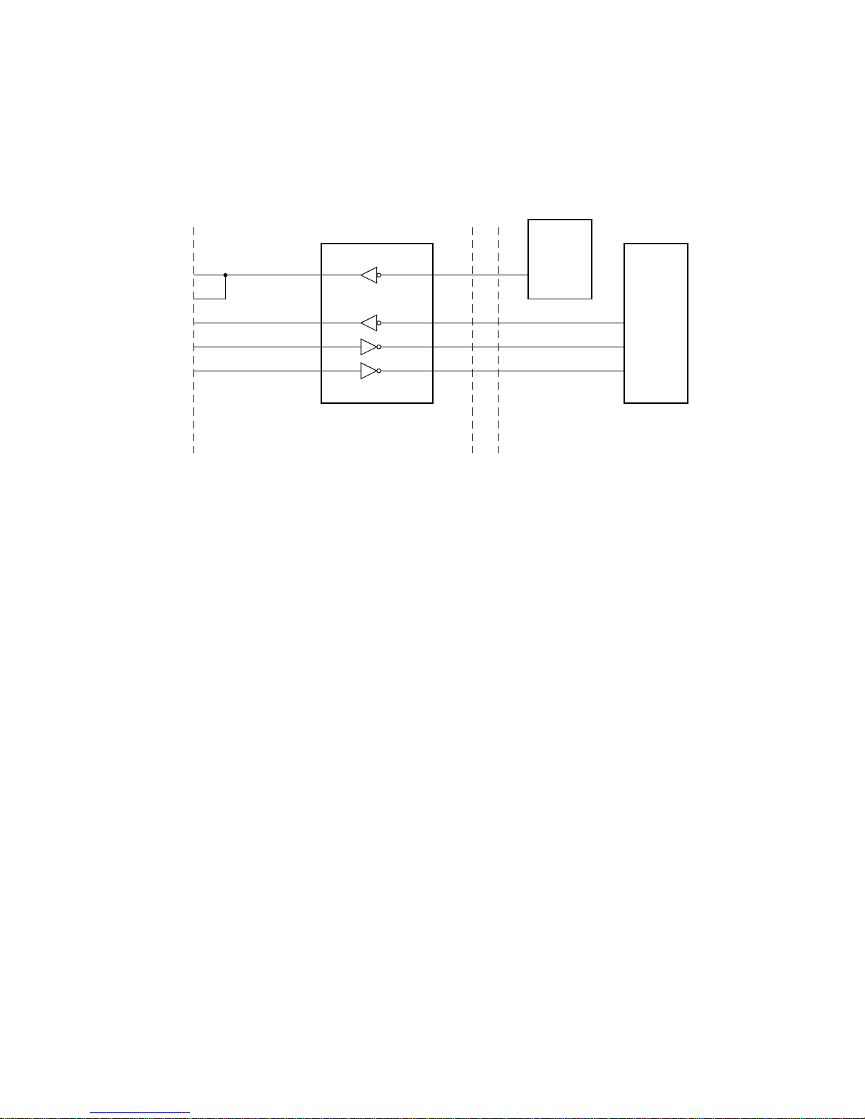
2-1-1. RS-232C Interface
Fig. 2-2 RS-232C Interface
Data from host to printer passes through the IC1 on the interface board from the RXD terminal and is input to the CPU on
the main logic board.
IC1 converts the RS-232C and TTL voltage levels.
The CPU converts the input serial data to parallel data and stores that data in the memory buffer memory. It also converts
the internal parallel data to serial data and outputs that to the IC1.
The CTS line is hardware-connected, but the connection is not recognized by software. (The printer does not monitor the
signal.)
D2O
D1O
R1I
R2I
D2I
D1I
R1O
R2O
B12
B14
A15
B15
ACKDTR
R-CH
TXD
RXD
CTS
TXD0
RXD0
RXD1
CN3 CN1
IC1
CN9
IC10
IC5
Gate
Array
CPU
HD151232FP
RS-232C Interface Board Main Logic Board
B12
B14
A15
B15
Page 19
– 19 –
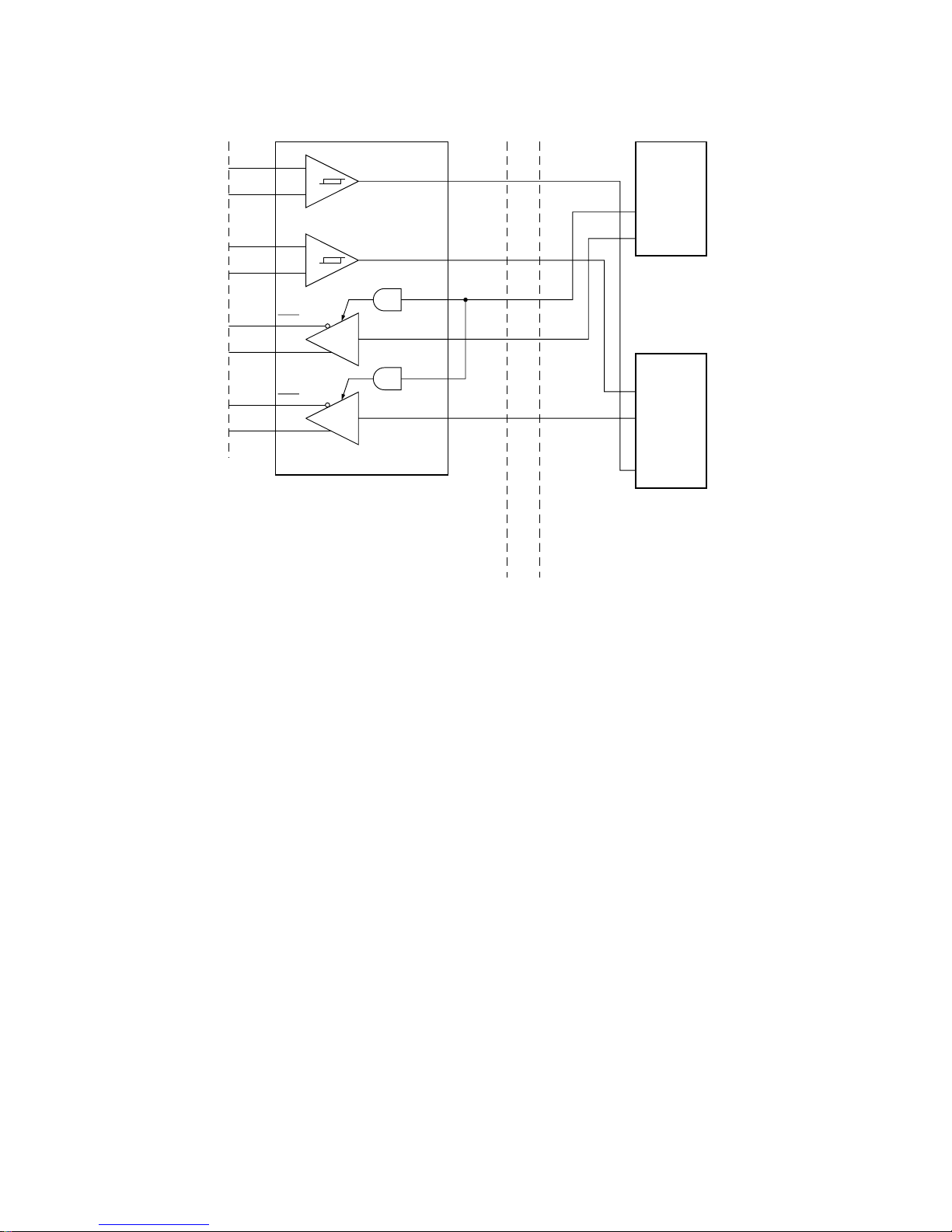
2-1-2. RS-422A Interface
Fig. 2-3 RS-422A Interface
Data flow from host to printer passes from the RD terminal to the IC1 on the interface board and is input to the CPU.
The IC1 converts the RS-422A and TTL voltage levels.
The CPU converts the input serial data to parallel data and stores that data in the memory buffer memory. It also converts
the internal parallel data to serial data and outputs that to the IC1.
D2O
D1O
D2EN
D2I
D1EN
D1I
ERROR
ACK
RD (+)
RD (–)
CS (+)
CS (–)
RS (–)
RS (+)
SD (–)
SD (+)
CN3 CN1
IC1
+
–
+
–
Gate
Array
CN9 IC10
R2I
+
R2I
–
R1I
+
R1I
–
D2O
D2O
D1O
D1O
RXD0
TXD0
RXD1
CPU
IC5
A15
B15
A10
B12
B14
A15
B15
A10
B12
B14
MC34051
RS-422A Interface Board Main Logic Board
Page 20
– 20 –
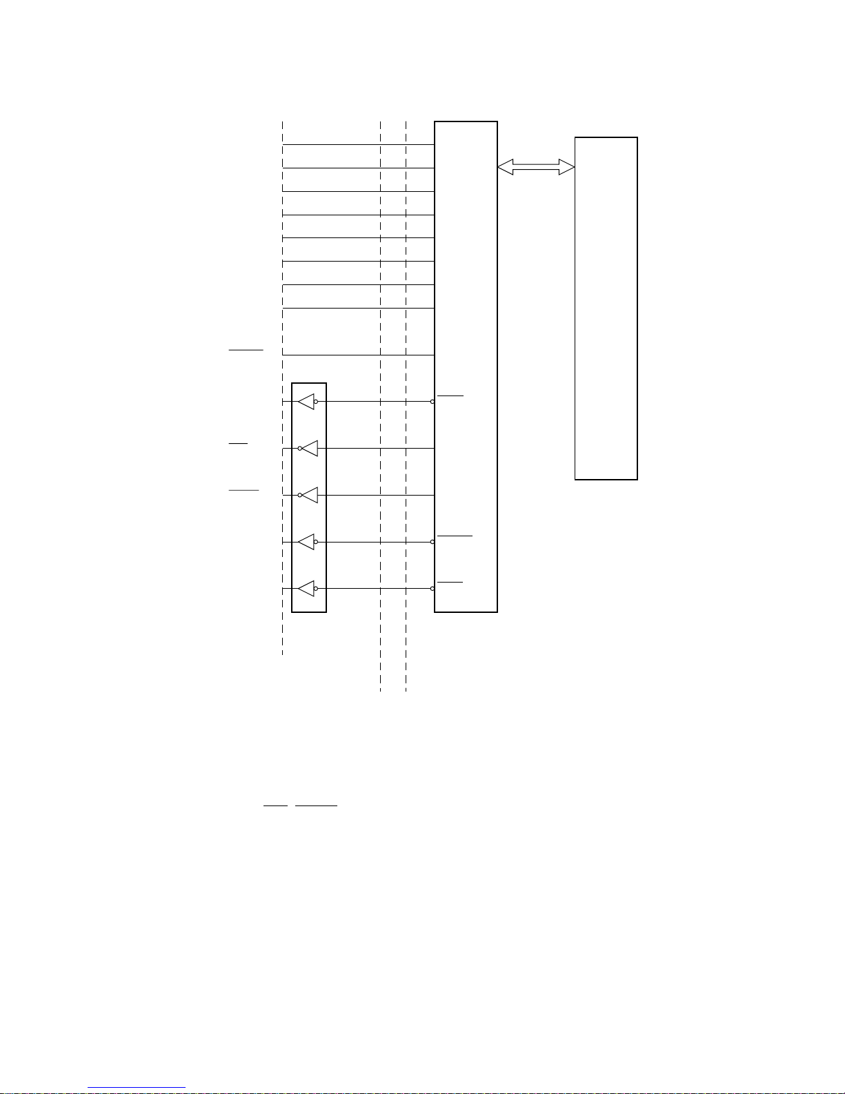
2-1-3. Parallel Interface
Fig. 2-4 Parallel Interface
The host computer sends eight bits of data for DATA 1 - 8 to the CN3 connector when the BUSY signal is LOW (printer
is ready).
The data passes through the interface board and gate array, then moves into the CPU.
Printer signals from the CPU (ACK, ERROR, SELECTED, PAPER OUT, etc.) pass through the gate array and are output
the appropriate connector pins.
DATA 1
DATA 2
DARA 3
DATA 4
DATA 5
DARA 6
DATA 7
DATA 8
STROBE
BUSY
ACK
ERROR
SELECTED
PAPER OUT
A4
B4
A5
B5
A6
B6
A7
B7
A13
A12
B12
A10
A11
B11
CN3
CPU
CN1
IC5
CN9
A4
B4
A5
B5
A6
B6
A7
B7
A13
A12
B12
A10
A11
B11
Gate Array
IC10
LS05
IC1
CD0
CD1
CD2
CD3
CD4
CD5
CD6
CD7
CSTB
BUSY
ACK
ERROR
SELECT
POUT
Parallel Interface Board Main Logic Board
Page 21
– 21 –
2-2. Editing and Printing
2-2-1. Editing
The CPU reads data sequentially from RAM and edits it in accordance with program instructions stored in EPROM. The
edited data undergoes parallel-to-serial conversion in the gate array, and is then output to the thermal head’s drive
controller.
2-2-2. Thermal Head
The thermal head contains 640 heat elements. Printing is carried out by switching these elements ON or OFF as required.
(Note that Line Mode supports 600-dot printing only. Heat elements numbered 1 to 20 and 621 to 640 are always off.
(Off data is always being transmitted.)) The thermal head has a built-in dedicated drive controller. The controller consists
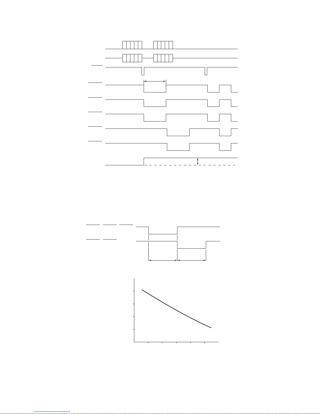
of a shift register, a latch circuit, and a driver circuit, as illustrated below.
The drive controller receives serial data (SI) from the drive control board in sync with the CLOCK signal. The controller
latches the incoming data (LATCH), then outputs it to the heat elements in sync with the trailing edge of the STROBE
signals. A data value of LOW corresponds to a heat-element value of ON.
Fig. 2-5 Thermal-Head Drive Circuit
STROBE5
STROBE4
STROBE3
STROBE2
STROBE1
LATCH
SI
CLOCK
COM
Latch
Shift Resistor
Page 22
– 22 –
Fig.2-6 Timing Chart
2-2-3. Head Current Control
Heat buildup in the head during operation can cause print quality to degrade. To maintain uniform printing quality, the
printer varies the energizing time (time that STROBE remains LOW) in accordance with the head temperature.
The thermal head’s surface temperature is calculated based on the resistance value of an attached thermistor. Energizing
time is reduced at higher temperatures, as indicated in the Figure 2-6.
Fig. 2-7 Head Energizing Control
24V
t
CLOCK
SI
LATCH
STROBE1
STROBE2
STROBE3
STROBE4
STROBE5
COMMON
STROBE1, STROBE2, STROBE3
STROBE4, STROBE5,
t t
10 20 30 40 50
300
400
500
Head Energizing Time t (µsec)
Thermistor Temp. °C
600
Page 23
– 23 –
2-3. Feed-Motor Drive Circuit
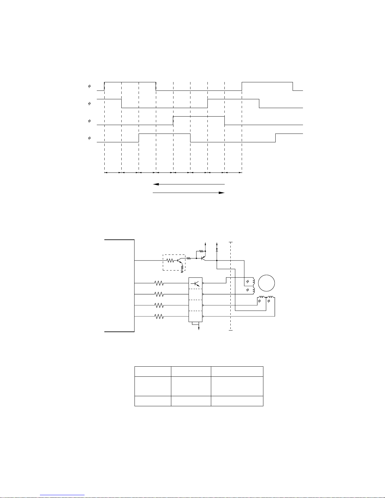
This printer employs a paper feed motor and a stepping motor. The motor rotates through a certain angle each time it
receives a pulse from the drive circuit. This printer employs a 4-phase stepping motor and controls the paper feed motor
with a phase 1-2 excitation method. The following diagram illustrates the phase 1-2 excitation method. Diagram 2-8
shows the feed-motor drive circuit.
Fig. 2-8 Motor Control by Phase 1-2 Excitation
Fig. 2-9 Feed-Motor Drive Circuit
Voltage to the motor is controlled to produced the required action, as follows.
Mode Voltage Action
Operating VM (+24V) Drives the motor
VL (+5V)
Idle VL (+5V) Holds the motor
Voltage is controlled by PA4 pin of the CPU, which goes HIGH or LOW to switch transistors DQ2 and Q2 ON and OFF.
When Q2 is ON, the paper feed motor receives VM (+24V). When Q2 is OFF, VL (+5V) is supplied to the motor via
diode D1.
1 2 3 4 5 6 7 8
1
2
3
4
ON
ON
ON
ON
ON
Step
Reverse Feed
Forward Feed
PA4
PA0
PA2
PA3
PA1
1
2
3
4
CN4
1
2
4
5
6
3
M
+5V+24V
Q2
D1
TA1
B
DQ2
M-GND
E
IC5
CPU
Paper Feed Motor
Page 24
– 24 –
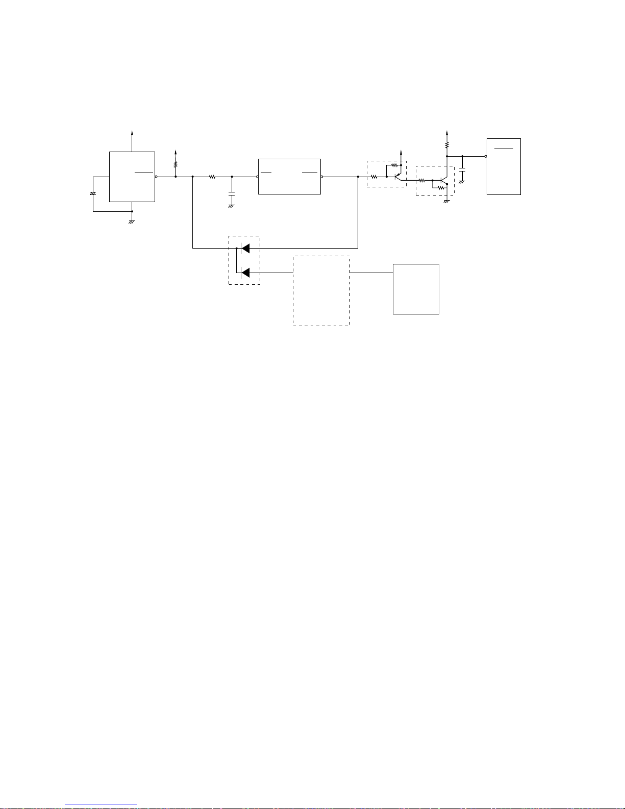
2-4. Power-On Reset Circuit
Immediately following power-on the printer executes a power-on reset, initializing all circuit elements. The power-on
reset serves as protection against operational errors. The power-on RESET signal is maintained for approximately 160ms.
The reset circuit is illustrated below.
Fig. 2-10 Power-On Reset Circuit
(1) At power on, voltage-detector circuit IC4 (M51953BL) outputs a LOW signal from its OUT terminal.
The following formula is used by capacitor C2 (0.47µF).
T = 0.34 × C2 (pF) [µs] = 160ms
(2) The LOW signal resets the CPU and the mechanism drive circuits.
(3) The LOW signal sets S-RAM into backup status.
+5V
IC4
CD
C2
GND
+5V
+5V
+5V
VCC
RESET
DD3
IC5 : CPU
RES
RESO
RESET
VCC
S-RAM
+
Gate
Array
IC1
RESET IC
IC10
Protection
Circuit
CPU
Page 25

– 25 –
2-5. +5V Line Voltage Detector Circuit
The voltage-detection IC detects momentary drops or unstable levels in the +5V line voltage.
The following illustrates the equivalence circuit of the voltage detector IC (Fig. 2-9 IC4).
Fig. 2-11 Equivalence Circuit for Voltage Detecting IC
The following operation timing chart shows control is performed by the voltage detector IC output. If the +5V line voltage
falls below 4.25V, the IC produces a reset signal from its OUT terminal, resetting the CPU and the gate array.
Fig. 2-12 Operation Timing Chart
1.25V
R1
R2
SµA typ
V
CC
1
GND
3
Cd
4
–
OUT
5
–
+
VCC Voltage
4.25V
0.8V
Output
Voltage
tdtd
t
t
td = 0.34 × Cd (pF) [µs]
Page 26

– 26 –
3. Printer Mechanism
3-1. Thermal Head
TSP400 series printers employ thermal line printing. The thermal head consists of a horizontal line of 640 heat elements.
These elements print one line of dots at a time as the paper passes over the head. The head is fixed in position; only the paper
moves.
The printer prints a dot by heating the corresponding heat element. The heated element causes a chemical reaction in the
coloring layer of the thermal paper, resulting in the formation of a visible dot.
Fig. 2-13 Principle of Thermal Printing
3-2. Paper-Feed Mechanism
The paper-feed mechanism is comprised of the paper-feed motor, gear train, platen, and thermal head. The paper-feed motor
drives the gear train, which in turn rotates the platen. The platen carries the thermal paper past the thermal head.
The paper-feed motor is a PM (permanent magnet) type, 4-phase 48-pole stepping motor. A single step feeds the paper
approximately 0.125mm.
Fig. 2-14 Paper-Feed Mechanism
Thermal Printing Head
Heat Element
Coloring Layer
Thermal Paper
Printed Point
Platen Roller
Gear Train
Paper-feed Motor
Platen Roller
Thermal Paper
Thermal Head
Page 27

– 27 –
3-3. Sensor
(1) Paper-Out Sensor
The paper-out sensor is located at the paper entry slit. The detector consists of a reflective photosensor. The
photosensor’s phototransistor remains ON while paper is present. It goes OFF when paper runs out, generating
output of a paper-out signal.
(2) Black-Mark Sensor
This detector senses black marks indicating print start positions. The detector is useful only with specially marked
paper. Like the paper-out detector, the black-mark detector consists of a reflective photosensor. The photosensor’s
phototransistor goes OFF when a black mark appears.
Fig. 2-15 Paper-Out Detector Fig. 2-16 Black-Mark Detector
(3) Paper Near-end Sensor
The Paper Near-end Sensor detects the amount of paper remaining on the roll. When the roll paper no longer exists
at the set position, the reflective photosensor turns OFF and outputs a no paper signal.
Fig. 2-17 Paper Near-end Sensor
GND
+5V
R
R
GND
+5V
R
R
Paper
(Reflective Photosensor)
Detection Signal
Paper
Black Mark
(Reflective Photosensor)
Detection Signal
GND
+5V
R
R
Paper
(Reflective Photosensor)
Detection Signal
Page 28

– 28 –
(4) Head-Up Detector
This detector consists of a leaf switch indicating whether the head is closed (in contact with the platen) or open
(separated from the platen). The leaf switch is closed when the head is closed; it opens when the head is opened.
Fig. 2-18 Head-Up Detector
GND
Detection Signal
Leaf Switch
R
+5V
Page 29

CHAPTER 3
PARTS REPLACEMENT AND RELATED ADJUSTMENTS
This chapter describes disassembly and reassembly procedures.
Please take note of the following.
1. ALWAYS disconnect the power cord from the AC outlet before beginning a disassembly or reassembly
procedure.
2. Except where otherwise stated, the reassembly procedure is the reverse of the disassembly procedure.
3. Coat screw heads with locking sealant after completion of reassembly.
4. Refer to Chapter 4 Section 2 for important information about lubrication requirements.
Note:The printer has no adjustable parts.
1. Presenter (TUP482) ........................................................................................... 30
2. Cutter.................................................................................................................. 30
3. Printer Mechanism ............................................................................................31
4. Main Logic Board ..............................................................................................31
5. Print Head Unit .................................................................................................. 32
6. Feed Motor Assembly ....................................................................................... 32
7. Sensor Unit ........................................................................................................ 33
3
Page 30

– 30 –
1. Presenter (TUP482)
(1) Disconnect the power cord from the AC outlet.
(2) Remove:
• Screws 4 pcs. [1]
• Presenter Holder L and R [2]
• Presenter [3]
Refer to Step 4 to remove the connector which is
connected to the main logic board from the
Presenter.
2. Cutter
(2) Remove:
• The presenter in Step 1.
• Screws 5 pcs. [1]
• Cutter Holder L and R [2]
• Cutter [3]
Refer to Step 4 to remove the connector which is
connected to the main logic board from the Cutter.
[2]
[3]
[1]
[2]
[1]
[2]
[1]
[3]
[1]
[2]
Page 31

– 31 –
3. Printer Mechanism
(1) Remove the power supply connector.
(2) Remove:
• Screws 4 pcs. [1]
• Connector [2]
Cut the wire band in four places.
• Printer Mechanism [3]
Refer to Step 4 to remove the connector which is
connected to the main logic board from the printer
mechanims.
4. Main Logic Board
(1) Remove the power supply connector.
(2) Remove:
• Four screws [1]
• Wiring band
• Connectors
• Screws 4 pcs. [2]
• Main Logic Board [3]
When removing the wiring band, check which one is
the lead wire.
[1]
[2]
[3]
[1]
[2]
[1]
[3]
Page 32

– 32 –
5. Print Head Unit
(1) Pull the pressure stay [1] forward to open the head
frame unit [2].
(2) Slide the head clamp [3] in the direction indicated by
the arrow. Remove the print head unit [4].
(3) Remove the head connector [5].
Note :Be careful to avoid damaging the heat elements when
installing the replacement unit.
6. Feed Motor Assembly
(1) Remove:
• Printer mechanism (See 3. above.)
• Wiring band holding the lead wire.
• Screws 2 pcs. [1]
• Feed motor [2]
[2]
[1]
[4]
[5]
[2]
[1]
[3]
Page 33

– 33 –
[3]
[2]
[1]
[4]
7. Sensor Unit
Old Type
(1) Remove:
• Printer mechanism (See 3. above.)
• Two wire band screws holding the lead wire [1].
• Screws 2 pcs. [1]
• Transmit sensor [2]
• Screw 1 pc. [3]
• Head-up sensor [4]
Note:There are two types of transmit sensors.
One is for the old type and the other is for the new type.
New Type
[3]
[2]
[1]
[4]
Page 34

This page was intentionally left blank.
Page 35

4
CHAPTER 4
MAINTENANCE AND LUBRICATION
This chapter explains printer maintenance and lubrication.
1. Maintenance ...................................................................................................... 36
1-1. Cleaning ................................................................................................................ 36
1-2. Checks................................................................................................................... 36
2. Lubrication......................................................................................................... 37
2-1. Lubricants ............................................................................................................. 37
2-2. Application Method .............................................................................................. 37
2-3. Lubrication Points................................................................................................ 37
Page 36

– 36 –
1. Maintenance
Proper maintenance is necessary to maintain printer performance and forestall potential problems. Please carry out
maintenance as described below.
1-1. Cleaning
(1) Surface dirt
Clear away dirt with a soft cloth. If necessary, apply a small quantity of alcohol to the cloth to improve cleaning
power. NEVER use thinner, trichlene, or ketone solvents, as these can cause damage to plastic components.
When cleaning, take care to avoid damaging or moistening of electronic parts, mechanical parts, and wires.
(2) Internal dust
For best results, use an electric vacuum cleaning device to remove dust from the inside of the printer. Note that such
cleaning may also remove lubrication; when you have finished cleaning, check lubrication levels and apply
lubricant as necessary.
1-2. Checks
There are two types of maintenance checks. Simple “daily checks” can be performed by users during the course of daily
operation. “Periodic checks” must be carried out by qualified service personnel.
(1) Daily checks
• Check whether dirt or other foreign matter has worked its way into the printer, and remove as necessary.
• Check the thermal head for excessive dirt. If the head is very dirty, clean it with a cotton stick or a soft cloth
soaked in alcohol.
(2) Periodic checks
Periodic checks and lubrication should be carried out once every six months or once every million lines of printing.
• Check the integrity of springs.
• Clear dust from areas around the detectors.
Page 37

– 37 –
2. Lubrication
Proper lubrication is essential for maintaining the printer’s performance level and preventing breakdowns or other problems.
2-1. Lubricants
Choice of lubrication can significantly affect the printer’s performance, longevity, and low-temperature characteristics. We
recommend the following lubricant for the TSP400 series.
Type Name Manufacturer
Grease Molykote EM Dow Corning
2-2. Application Method
If you are lubricating parts during disassembly or reassembly, be sure to wash or wipe the parts thoroughly to remove all
dirt and dust prior to lubricating.
Remember that cleaning can remove necessary lubrication. Always lubricate after cleaning, disassembly, or replacement.
2-3. Lubrication Points
Apply lubricants at the following locations. (Refer to Diagram 4-1.)
No. Location
[1] Contact area of pressure bar and pressure pin
[2] Contact area of gear 15×50×0.5 and gear shaft
[3] Contact area of gear 58×0.5 and gear shaft
[4] Contact area of gear 15×50×0.5 and PF motor gear
[5] Contact area of gear 58×0.5 and platen gear
[6] Contact area of head stay and head base frame
[7] Contact area of head clamp and clamp pin
[8] Contact area of head clamp and head stay R
Page 38

– 38 –
B
A
C
D
D
A
B
C
C
[5]
[2]
[4]
[3]
[1]
[6]
[6]
[7]
[8]
[1]
Fig. 4-1 Lubrication Points
Page 39

5
CHAPTER 5
PARTS LIST
HOW TO USE PARTS LIST
(1) DRWG. NO.
This column shows the drawing number of the illustration.
(2) REVISED EDITION MARK
This column shows a revision number.
Part that have been added in the revised edition are indicated with "#"
Part that have been abolished in the revised edition are indicated with "*"
#1:First edition → Second edition *1:First edition → Second edition
(3) PARTS NO.
Parts numbers must be notified when ordering replacement parts. Parts described as "NPN" have no parts number
and are not in stock, unavailable.
(4) PARTS NAME
Parts names must be notified when ordering replacement parts.
(5) Q’TY
This column shows the number of the part used as indicated in the figure.
(6) REMARKS
This column is used for general comments. It also indicates EPROM seal numbers. A"*" within a seal number
indicates the version number.
(7) RANK
Parts marked “S” are service parts. Service parts are recommended to be in stock for maintenance.
9. RS-422A Interface Board.................69
9-1. Circuit Diagram.........................69
9-2. Component Layout...................70
9-3. Parts List ...................................70
10. Parallel Interface Board (Ver. 1) .....71
10-1.Circuit Diagram........................71
10-2.Parts List ..................................72
11. Parallel Interface Board (Ver. 2) .....73
11-1.Circuit Diagram........................73
11-2.Component Layout..................74
11-3.Parts List ..................................74
12. Near-End Sensor Board ..................75
12-1.Circuit Diagram........................75
12-2.Parts List ..................................75
13. Paper-End Sensor Board ................76
13-1.Circuit Diagram........................76
13-2.Parts List ..................................76
14. Transit Board ...................................77
14-1.Circuit Diagram........................77
14-2.Parts List ..................................77
15. Presenter Sensor Board..................78
15-1.Circuit Diagram........................78
15-2.Parts List ..................................78
1. Printer Assembly .............................40
1-1. Disassembly Drawing ..............40
1-2. Parts List ...................................41
2. Printer Mechanism...........................42
2-1. Disassembly Drawing ..............42
2-2. Parts List ...................................43
3. Presenter-Assembly ........................44
3-1. Disassembly Drawing ..............44
3-2. Parts List ...................................45
4. Wiring Scheme of printer ................46
4-1. RS232 Interface Type ...............46
4-2. RS-422A Interface Type ...........47
4-3. Parallel Interface Type .............48
5. Main Logic Board (Ver.1) ................49
5-1. Circuit Diagram.........................49
5-2. Parts List ...................................53
6. Main-Logic Board (Ver.2) ................56
6-1. Circuit Diagram.........................56
6-2. Component Layout...................61
6-3. Parts List ...................................62
7. RS-232C Interface Board (Ver. 1) ...65
7-1. Circuit Diagram.........................65
7-2. Parts List ...................................66
8. RS-232C Interface Board (Ver. 2) ...67
8-1. Circuit Diagram.........................67
8-2. Component Layout...................68
8-3. Component Layout...................68
Page 40

– 40 –
1. Printer Assembly
1-1. Disassembly Drawing
17
13
30
16
15
13
38
16
12
33
29
14
34
18
18
19
3736
B
20
21
A
F
K
E
G
H
C
D
L
C
K
J
E
F
G
H
D
I
I
J
22
25
32
A
1
4
2
2
31
23
24
5
6
11
9
2
B
10
28
2
26
3
35
39
7
27
L
27
8
Page 41

– 41 –
1 01903059 SCREW TR 3-5 FL 3 S
2 *1 01903077 SCREW TAT 3-5 CT-FL 41 S
#1 01903101 SCREW TAT 3-6 CT-FL 41 S
3 30721610 CUTTER CABLE UNIT TUP4 1 TUP452,TUP482VER.1
4 32000050 FRAME R TUP4 1
5 32002211 BOTTOM FRAME TUP4 1
6 32005120 PAPER FRAME L TUP4 1
7 32041130 SNOUT HOLDER L TUP4 1 TUP482
8 32041140 SNOUT HOLDER R TUP4 1 TUP482
9 02040402 FLANGED NUT NHW4 1 S
10 31303211 ARM SHAFT TUP4 1
11 32000060 FRAME L TUP4 1
12 37427400 TRANSIT BOARD UNIT TUP4 1 S
13 30510510 SPRING E050-035-0235 2 S
14 32003211 FRONT FRAME TUP4 1
15 32005020 CUSHION FRAME L TUP4 1
16 33390010 CUSHION SHAFT TUP4 2
17 83390020 ROLL PAPER SHAFT SP312 1
18 37422500 PUSH SWITCH UNIT TUP4 1
19 04991401 SCREW DBLC-J25SAF 2 RS232,RS422 S
20 32003020 REAR PLATE TUP4 1
21 37407800 RS232C IF BOARD UNIT TSP4 1 RS232 VER.1
#1 37427620 INTERFACE BOARD R232 UNIT T4V2 1 RS232 VER.2
37407810 RS422 IF BOARD UNIT TSP4 1 RS422
37407820 PARALLEL IF BOARD UNIT TSP4 1 PARALLEL VER.1
#1 37427610 INTERFACE BOARD PARA UNIT T4V2 1 PARALLEL VER.2
22 37420310 PAPER FRAME R UNIT TUP4 1
23 37420510 COVER FRAME UNIT TUP4 1
24 37427000 MAIN LOGIC BOARD UNIT TUP4 1 VER.1 S
37427030 MAIN LOGIC BOARD UNIT T4V2 1 VER.2 S
25 37427300 NE BOARD UNIT TUP4 1 S
26 38405400 TMP452W-24N 1 S
27 01903090 SCREW TAT 3-8 CT-FL 2 TUP482 S
28 33490210 ARM TUP4 1
29 32005311 MECHANISM FRAME TUP4 1
30 32005010 CUSHION FRAME R TUP4 1
31 82020361 ROM COVER SP312 1
32 30093010 ESD GUARD SHEET TUP4 1
33 09990713 FERRITE CORE TFC-16-8-16 1
34 30721650 POWER CABLE UNIT TUP4 1
35 38511201 PR112-24 1 TUP482
36 32021010 SERIAL IF PLATE TSP4 1 RS232,RS422
32021110 PARALLEL IF PLATE TSP4 1 PARALLEL
37 #1 30091010 TENSION SHEET TSP2 1
38 #1 30992010 DISCHARGE BRUSH T4V2 1 TUP482 VER.2
39 #1 30992020 DISCHARGE SHEET T4V2 1 TUP482 VER.2
DRWG.NO. REV. PARTS NO. PARTS NAME Q’TY REMARKS RANK
Printer Assembly
1-2. Parts List
Page 42

– 42 –
2. Printer Mechanism
2-1. Disassembly Drawing
13-6
13-14
13-12
13-10
13-5
13-11
13-3
13
13-9
13-12
28
16
16
14
13-9
19
13-2
13-1
13-6
13-10
13-14
13-12
15
15
13-7
13-13
13-8
13-7
13-13
13-15
9
7
4
11
1-2
1-3
28
6
1
11
28
6
5
17
3
18
10
22
1-4
1-1
13-12
24
12
19
23
23
25
21
21
8
21
26
21
2
2
20
27
B
A
D
C
D
C
B
A
(New Type)
(Old Type)
2-1
Page 43

– 43 –
1 NPN FRAME ASSY TMP4 1
1-1 37412300 PF MOTOR ASSY TMP4 1 S
1-2 87340390 HEAD DETECTOR ASSY BMP8 1 S
1-3 00920503 SCREW TAT 2-5 CT 1 S
1-4 00930403 SCREW TAT 3-4 CT 2 S
2 37417000 REFLECT SENSOR BD UNIT TMP4 1 OLD TYPE S
37417020 TRANSMIT SENSOR BD UNIT B TMP4 1 NEW TYPE S
2-1 30721010 CABLE UNIT TMP4 1 S
3 83100460 IDLER GEAR 15X50X0.5 1 S
4 31375211 PLATEN TMP4 1 S
5 33102210 GEAR 28X0.5 TMP4 1 S
6 80203041 DRIVE SHAFT BEARING MP300 2 S
7 33910060 PAPER GUIDE C TMP4 1 S
8 04991509 CUTTER AC310-24-LN 1
9 *1 33910030 PAPER GUIDE B TMP4 1 S
#1 33910031 PAPER GUIDE B TMP4 1 S
10 33903010 FRICTION PLATE TMP4 1 S
11 33490010 HEAD POSITION LEVER TSP4 2
12 37419000 HEAD UNIT TMP4 1 S
13 NPN HEAD FRAME UNIT TMP4 1
13-1 81360850 PAPER GUIDE ROLLER BMP4 1
13-2 *1 81370920 HEAD UNIT HOLDER SHAFT BMP4 1
#1 31303010 HEAD UNIT HOLDER SHAFT TMP4 1
13-3 82902330 HEAD CLAMP BMP4 1
13-4 81370910 PRESSURE STAY BMP4 1
13-5 09991391 HEAT-SHRINK TUBE A-6.0 GRN 1
13-6 82401370 PRESSURE LEVER BMP4 2
13-7 82401360 HEAD STOPPER LEVER BMP4 2
13-8 80994252 GUARD SHEET BMP4 1
13-9 04310401 OILESS BUSHING F4X7X3 2
13-10 80511070 SPRING E040-040-0159 2 S
13-11 80510840 SPRING E055-060-0180 1 S
13-12 04020015 STOP RING SE3.0 4 S
13-13 04020016 STOP RING SE4.0 2 S
13-14 02040301 FLANGED NUT NHW3 2 S
13-15 09991372 HEAT-SHRINK TUBE 4.0 1 S
14 80705031 CABLE UNIT 26X290CC BMP4 1
15 30510410 SPRING E065-070-0238 2 S
16 30520210 SPRING C075-080-0165 2 S
17 04012003 ROLL PIN SP2.0X8 1 S
18 04020010 STOP RING SE2.0 1 S
19 04991204 FASTENER T18S 8 S
20 00630404 SCREW TR 3-4 2 S
21 01903077 SCREW TAT 3-5 CT-FL 5 S
22 01914035 SCREW TAT 4-10 PT-FL 1 S
23 00820304 SCREW TR 2-3 2 S
24 01903090 SCREW TAT 3-8 CT-FL 1 S
25 32041110 CUTTER HOLDER L TSP4 1
26 32041120 CUTTER HOLDER R TSP4 1
27 32045220 GUIDE B AC3 1
28 04020016 STOP RING SE4.0 5 S
DRWG.NO. REV. PARTS NO. PARTS NAME Q’TY REMARKS RANK
Printer Mechanism
2-2. Parts List
Page 44

– 44 –
3. Presenter-Assembly
3-1. Disassembly Drawing
10
2
11
2-1
2-3
2-4
2-2
2-5
2-6
6
7
12
1
8
13
11
6
5
4
3
3-1
9
4-1
Page 45

– 45 –
1 37517000 DETECTOR BOARD UNIT PR1 1 S
2 37514010 SLIP GEAR UNIT PR1 1 S
2-1 33120210 SLIP WHEEL PR1 1
2-2 33101410 SLIP GEAR PR1 1
2-3 32012010 SLIP PLATE PR1 1
2-4 30520510 SPRING C111-080-0090 1
2-5 04020017 STOP RING SE5.0 1
2-6 02206002 PLAIN WASHER WF6X13X1.0 1
3 37513010 PAPER FEED ROLLER UNIT PR1 1
3-1 04300781 O-RING 7.8X1.9JIS3P8 1 S
4 37512010 PAPER FEED MOTOR UNIT PR1 1
4-1 33140020 WORM GEAR PR1 1 S
5 37510010 FRAME UNIT PR1 1
6 33215010 PF ROLLER BEARING PR1 2
7 32025010 UPPER COVER PR1 1
8 30045040 GUIDE D PR1 1 S
9 30045011 GUIDE A PR1 1 S
10 04033001 PUSH RIVET P3035B 2
11 04020010 STOP RING SE2.0 2 S
12 00930609 SCREW TAT 3-6 CT 1 S
13 00820304 SCREW TR 2-3 2 S
DRWG.NO. REV. PARTS NO. PARTS NAME Q’TY REMARKS RANK
Presenter-Assembly
3-2. Parts List
<Note 1> If DRWG. NO. 10 is removed, it should be replaced with new ones.
Page 46

– 46 –
4. Wiring Scheme of Printer
4-1. RS232 Interface Type
1
2
3
4
5
6
7
8
9
10
11
12
13
14
15
16
17
18
19
20
21
22
23
24
25
A1
A2
A3
A4
A5
A6
A7
A8
A9
A10
A11
A12
A13
A14
A15
A16
A17
A18
A19
A20
B1
B2
B3
B4
B5
B6
B7
B8
B9
B10
B11
B12
B13
B14
B15
B16
B17
B18
B19
B20
1
2
3
4
5
6
CN2
CN3
RS232C I/F BOARD
F-GND
TXD
RXD
RTS
CTS
NC
GND
NC
NC
NC
RCH
NC
GND
FAULT
MP-TXD
MP-DTR
NC
NC
NC
DTR
NC
NC
NC
NC
NC
NC
NC
VVR
DIN1
DIN3
DIN5
DIN7
GND
Vcc(+5V)
NC
NC
NC
DIEN
GND
RXD
NC
ID2
GND
PEXT1
VEXT
NC
NC
GND
DIN2
DIN4
DIN6
DIN8
GND
Vcc(+5V)
NC
FAULT
DTR
GND
TXD
CTS
ID1
GND
PSWIN
PEXT2
VEXT
DIN9
DIN11
VVR
DIN1
DIN3
DIN5
DIN7
GND
Vcc(+5V)
ERR
SLCT
BUSY
STB
GND
RXD
ID0
ID2
GND
PEXT1
VEXT
DIN10
DIN12
GND
DIN2
DIN4
DIN6
DIN8
GND
Vcc(+5)
NMI
PE
ACK
GND
TXD
CTS
ID1
GND
PSWIN
PEXT2
VEXT
1
2
3
4
5
6
7
1
2
1
2
3
4
5
6
1
2
3
4
1
2
3
GND
PE
MARK
Vcc(+5)
LABLE
GND
LED
HUP DTCT
HUP DTCT
LFCMN
LFCMN
LFø1
LFø3
LFø4
LFø2
1
2
3
4
5
6
7
8
9
10
11
12
13
14
15
16
17
18
19
20
21
22
23
24
25
26
1
2
3
4
1
2
3
4
5
1
2
3
4
5
6
7
8
9
10
11
12
13
14
15
16
17
18
19
20
21
22
23
24
25
26
COM(+24V)
COM(+24V)
COM(+24V)
GND
GND
GND
SI
SO
CLK
GND
LAT
GND
STB5
V
DD(+5V)
STB3
STB4
STB1
STB2
TM1
TM2
GND
GND
GND
COM(+24V)
COM(+24V)
COM(+24V)
CUTSW
CUTSW
M(–)
M(+)
VP(+24V)
VP(+24V)
NC
P-GND
P-GND
F-GND
PEXT1
VEXT
VEXT
PEXT2
PSW
1
2
3
4
5
Vcc(+5V)
PEXT1
VP(+24V)
PSWIN
GND
CUTTER UNIT
CN1
CONTROL BOARD PRINTER MECHANISM
CN9 CN1 CN1
CN1
MARK
DETECTOR
PAPER OUT
DETECTOR
HADE UP DETECTOR
PAPER FEED MOTOR
ø1
ø3
ø2 ø4
M
THERMAL HEAD
M
CN2
CN4
CN6
CN5
CN3
A1
A2
A3
A4
A5
A6
A7
A8
A9
A10
A11
A12
A13
A14
A15
A16
A17
A18
A19
A20
B1
B2
B3
B4
B5
B6
B7
B8
B9
B10
B11
B12
B13
B14
B15
B16
B17
B18
B19
B20
CONNECTED BOARD
CN5
1
2
3
4
5
6
7
GND
PE
MARK
Vcc(+5)
LABLE
GND
LED
CN4
1
2
3
4
5
6
7
8
HUP DTCT
HUP DTCT
LFCMN
LFCMN
LFø1
LFø3
LFø4
LFø2
1
2
3
4
5
6
CN1
1
2
CN2
1
2
3
4
5
6
7
CN3
PRESENTER
1
2
3
4
5
CN1
CN8
NEAR-END DETECTOR
1
2
3
4
5
6
7
8
9
CN1
GND
COPEN
PF-SW
OL-SW
PSW1
PSW2
PSW
OL-LED
PO-LED
1
2
3
4
5
6
7
8
9
10
11
12
CN7
GND
COPEN
PF-SW
OL-SW
PSW1
PSW2
PSW
OL-LED
PO-LED
HU-LED
ER-LED
Vcc(+5V)
RESUME SWITCH
1
2
3
4
[CN2]
(TUP482 only)
GND
PE
MARK
Vcc(+5)
LABLE
GND
LED
HUP DTCT
HUP DTCT
LFCMN
LFCMN
LFø1
LFø3
LFø4
LFø2
Page 47

– 47 –
A1
A2
A3
A4
A5
A6
A7
A8
A9
A10
A11
A12
A13
A14
A15
A16
A17
A18
A19
A20
B1
B2
B3
B4
B5
B6
B7
B8
B9
B10
B11
B12
B13
B14
B15
B16
B17
B18
B19
B20
DIN9
DIN11
VVR
DIN1
DIN3
DIN5
DIN7
GND
Vcc(+5V)
ERR
SLCT
BUSY
STB
GND
RXD
ID0
ID2
GND
PEXT1
VEXT
DIN10
DIN12
GND
DIN2
DIN4
DIN6
DIN8
GND
Vcc(+5)
NMI
PE
ACK
GND
TXD
CTS
ID1
GND
PSWIN
PEXT2
VEXT
1
2
3
4
5
6
7
1
2
1
2
3
4
5
6
1
2
3
4
1
2
3
GND
PE
MARK
Vcc(+5)
LABLE
GND
LED
HUP DTCT
HUP DTCT
LFCMN
LFCMN
LFø1
LFø3
LFø4
LFø2
1
2
3
4
5
6
7
8
9
10
11
12
13
14
15
16
17
18
19
20
21
22
23
24
25
26
1
2
3
4
1
2
3
4
5
1
2
3
4
5
6
7
8
9
10
11
12
13
14
15
16
17
18
19
20
21
22
23
24
25
26
COM(+24V)
COM(+24V)
COM(+24V)
GND
GND
GND
SI
SO
CLK
GND
LAT
GND
STB5
V
DD(+5V)
STB3
STB4
STB1
STB2
TM1
TM2
GND
GND
GND
COM(+24V)
COM(+24V)
COM(+24V)
CUTSW
CUTSW
M(–)
M(+)
VP(+24V)
VP(+24V)
NC
P-GND
P-GND
1
2
3
4
5
Vcc(+5V)
PEXT1
VP(+24V)
PSWIN
GND
CUTTER UNIT
CONTROL BOARD PRINTER MECHANISM
CN9 CN1 CN1
CN1
MARK
DETECTOR
PAPER OUT
DETECTOR
HADE UP DETECTOR
PAPER FEED MOTOR
ø1
ø3
ø2 ø4
M
THERMAL HEAD
M
CN2
CN4
CN6
CN5
CN3
CONNECTED BOARD
CN5
1
2
3
4
5
6
7
GND
PE
MARK
Vcc(+5)
LABLE
GND
LED
CN4
1
2
3
4
5
6
7
8
HUP DTCT
HUP DTCT
LFCMN
LFCMN
LFø1
LFø3
LFø4
LFø2
1
2
3
4
5
6
CN1
1
2
CN2
1
2
3
4
5
6
7
CN3
PRESENTER
1
2
3
4
5
CN1
CN8
NEAR-END DETECTOR
1
2
3
4
5
6
7
8
9
CN1
GND
COPEN
PF-SW
OL-SW
PSW1
PSW2
PSW
OL-LED
PO-LED
1
2
3
4
5
6
7
8
9
10
11
12
CN7
GND
COPEN
PF-SW
OL-SW
PSW1
PSW2
PSW
OL-LED
PO-LED
HU-LED
ER-LED
Vcc(+5V)
RESUME SWITCH
1
2
3
4
[CN2]
(TUP482 only)
GND
PE
MARK
Vcc(+5)
LABLE
GND
LED
HUP DTCT
HUP DTCT
LFCMN
LFCMN
LFø1
LFø3
LFø4
LFø2
1
2
3
4
5
6
7
8
9
10
11
12
13
14
15
16
17
18
19
20
21
22
23
24
25
1
2
3
4
5
6
CN2
CN3
RS422A I/F BOARD
F-GND
NC
NC
NC
NC
NC
GND
NC
SD(+)
SD(–)
NC
NC
GND
FAULT
NC
NC
RD(+)
RD(–)
CS(+)
NC
NC
NC
CS(–)
RS(+)
RS(–)
DIN9
DIN11
VVR
DIN1
DIN3
DIN5
DIN7
GND
Vcc(+5V)
DOEN
NC
NC
DIEN
GND
RD
ID0
ID2
GND
PEXT1
VEXT
DIN10
DIN12
GND
DIN2
DIN4
DIN6
DIN8
GND
Vcc(+5V)
NC
FAULT
RS
GND
SD
CS
ID1
GND
PSWIN
PEXT2
VEXT
F-GND
PEXT1
VEXT
VEXT
PEXT2
PSW
CN1
A1
A2
A3
A4
A5
A6
A7
A8
A9
A10
A11
A12
A13
A14
A15
A16
A17
A18
A19
A20
B1
B2
B3
B4
B5
B6
B7
B8
B9
B10
B11
B12
B13
B14
B15
B16
B17
B18
B19
B20
4-2. RS422A Interface Type
Page 48

– 48 –
A1
A2
A3
A4
A5
A6
A7
A8
A9
A10
A11
A12
A13
A14
A15
A16
A17
A18
A19
A20
B1
B2
B3
B4
B5
B6
B7
B8
B9
B10
B11
B12
B13
B14
B15
B16
B17
B18
B19
B20
DIN9
DIN11
VVR
DIN1
DIN3
DIN5
DIN7
GND
Vcc(+5V)
ERR
SLCT
BUSY
STB
GND
RXD
ID0
ID2
GND
PEXT1
VEXT
DIN10
DIN12
GND
DIN2
DIN4
DIN6
DIN8
GND
Vcc(+5)
NMI
PE
ACK
GND
TXD
CTS
ID1
GND
PSWIN
PEXT2
VEXT
1
2
3
4
5
6
7
1
2
1
2
3
4
5
6
1
2
3
4
1
2
3
GND
PE
MARK
Vcc(+5)
LABLE
GND
LED
HUP DTCT
HUP DTCT
LFCMN
LFCMN
LFø1
LFø3
LFø4
LFø2
1
2
3
4
5
6
7
8
9
10
11
12
13
14
15
16
17
18
19
20
21
22
23
24
25
26
1
2
3
4
1
2
3
4
5
1
2
3
4
5
6
7
8
9
10
11
12
13
14
15
16
17
18
19
20
21
22
23
24
25
26
COM(+24V)
COM(+24V)
COM(+24V)
GND
GND
GND
SI
SO
CLK
GND
LAT
GND
STB5
V
DD(+5V)
STB3
STB4
STB1
STB2
TM1
TM2
GND
GND
GND
COM(+24V)
COM(+24V)
COM(+24V)
CUTSW
CUTSW
M(–)
M(+)
VP(+24V)
VP(+24V)
NC
P-GND
P-GND
1
2
3
4
5
Vcc(+5V)
PEXT1
VP(+24V)
PSWIN
GND
CUTTER UNIT
CONTROL BOARD PRINTER MECHANISM
CN9 CN1 CN1
CN1
MARK
DETECTOR
PAPER OUT
DETECTOR
HADE UP DETECTOR
PAPER FEED MOTOR
ø1
ø3
ø2 ø4
M
THERMAL HEAD
M
CN2
CN4
CN6
CN5
CN3
CONNECTED BOARD
CN5
1
2
3
4
5
6
7
GND
PE
MARK
Vcc(+5)
LABLE
GND
LED
CN4
1
2
3
4
5
6
7
8
HUP DTCT
HUP DTCT
LFCMN
LFCMN
LFø1
LFø3
LFø4
LFø2
1
2
3
4
5
6
CN1
1
2
CN2
1
2
3
4
5
6
7
CN3
PRESENTER
1
2
3
4
5
CN1
CN8
NEAR-END DETECTOR
1
2
3
4
5
6
7
8
9
CN1
GND
COPEN
PF-SW
OL-SW
PSW1
PSW2
PSW
OL-LED
PO-LED
1
2
3
4
5
6
7
8
9
10
11
12
CN7
GND
COPEN
PF-SW
OL-SW
PSW1
PSW2
PSW
OL-LED
PO-LED
HU-LED
ER-LED
Vcc(+5V)
RESUME SWITCH
1
2
3
4
[CN2]
(TUP482 only)
GND
PE
MARK
Vcc(+5)
LABLE
GND
LED
HUP DTCT
HUP DTCT
LFCMN
LFCMN
LFø1
LFø3
LFø4
LFø2
1
2
3
4
5
6
7
8
9
10
11
12
13
14
15
16
17
18
19
20
21
22
23
24
25
26
27
28
29
30
31
32
33
34
35
36
1
2
3
4
5
6
CN2
CN3
PARALLEL I/F BOARD
STROBE
DATA 1
DATA 2
DATA 3
DATA 4
DATA 5
DATA 6
DATA 7
DATA 8
ACK
BUSY
PE
SLCT
NC
NC
GND
F-GND
Vcc(+5V)
RETURN-GND
RETURN-GND
RETURN-GND
RETURN-GND
RETURN-GND
RETURN-GND
RETURN-GND
RETURN-GND
RETURN-GND
RETURN-GND
RETURN-GND
RETURN-GND
INIT
ERROR
EXT-GND
CPL
NC
SLCT-IN
NC
NC
VVR
DIN1
DIN3
DIN5
DIN7
GND
Vcc(+5V)
ERROR
SLCT
BUSY
STB
GND
NC
ID0
NC
GND
PEXT1
VEXT
NC
NC
GND
DIN2
DIN4
DIN6
DIN8
GND
Vcc(+5V)
INIT
PE
ACK
GND
NC
NC
ID1
GND
PSWIN
PEXT2
VEXT
F-GND
PEXT1
VEXT
VEXT
PEXT2
PSW
CN1
A1
A2
A3
A4
A5
A6
A7
A8
A9
A10
A11
A12
A13
A14
A15
A16
A17
A18
A19
A20
B1
B2
B3
B4
B5
B6
B7
B8
B9
B10
B11
B12
B13
B14
B15
B16
B17
B18
B19
B20
4-3. Parallel Interface Type
Page 49

– 49 –
5. Main Logic Board (Ver.1)
5-1. Circuit Diagram
2
3
1
[VR2]
4.7K
VCC
2
3
1
[VR1]
47K
VCC
[R135]
220
[R101]
220
CN1
53014-0710
7654321
LABEL
MARK
PE
VCC
VP
CN8
53014-0510
<FOR PRESENTER>
12345
VEXT
ZD2
RD4. 7JSB1
R25
10K
R120
10K
C134
0.1U
Q4
A1649
R119
10K
VP
Q5
A1388
R17
10K
R124
10K
DQ5
FA1A4P
VH
VCC
8
5
IC8
VCC
GND
CSSKDI
DO
123
4
93C46
R18
33
C9
33P
C126
33P
C127
100P
C8
33P
R19
10K
VCC
DQ6
FA1A4P
DQ7
FN1A4P
VCC
323130292827262524232221201918
17
123456789
1011131415415756555254165160636162
59
47
I/O1
I/O2
I/O3
I/O4
IN5
IN6
IN7
IN8
HDPWR
IN9
IN10
IN11
IN12
IN13
IN14
IN15
IN16
CD0
CD1
CD2
CD3
CD4
CD5
CD6
CD7
CSTB
ACK
BUSY
ERROR
SELECT
POUT
HDONRDWRCERESET
CLK
INTCDT
INTSDT
RAMCS
PSOE
PSCE0
PSCE1
RFSH
UPD65622GF-TSP
SDATA
SCLK
HISTIN
LATCH
STB4
STB3
STB2
STB1
CUTON
CUTSW
OUT1
OUT2
OUT3
OUT4
A0A1A2
A3
A15
A17
D0D1D2D3D4D5D6
D7
VCC
VCC
TEST
PSSEL
GND
GND
GND
GND
4950464842434445403938373635696867666564797877767574737034728058123353
71
A0A1A2A3A15
A17D8D9
D10
D11
D12
D13
D14
D15
R21
R20
R23
R22
33 × 4
C129 C131
C128 C130
33P × 4
FL4
TU02M
VCC
2
31
C135
0.1U
VCC
JPB2
JPA2
5P8128 :
5P832 :
Standard
JPB2=Cut, JPA2=Short
R130
4.7K
R131
4.7K
VCC
R129
4.7K
R134
4.7K
CN7
53014-1210
121110
987654321
VCC
ER-LED
HU-LED
PO-LED
OL-LED
PSW
PSW2
PSW1
OL-SW
PF-SW
COPEN
GND
DQ3
FA1A4P
R161K1/2W
DQ4
FN1A4P
VP
Q1
D2010Q3B1359
CN5
5483-04A-RED
432
1
VCC
1
RA1
10K × 4
2435
C123 C120
C121
100P × 3
VH
COM
COM
GNDSICLK
/LAT
/STB5
/STB3
/STB1
TH1
GND
GND
COM
135791113151719212325
246
8
101214161820222426
COM
GND
GNDSOGND
GND
VDD
/STB4
/STB2
TH2
GND
COM
COM
CN6
5332-265G1
(AOI : J080-85523)
VH
VCC
C122
100P
THERMAL HEAD BLOCK
R128
20K
R127
1K
VCC
CN9
PHEC40R-R111
COMMUNICATION I/F BLOCK
EXPANDED I/O BLOCK
IC10
B
C
A
<Note 1> The unit of resistor and resistor array is "Ω", and no indication of wattage means 1/6W, 1/8 respectively.
<Note 2> The unit of capacitor and capacitor array is "F", and no indication of Voltage means 50V.
<Note 3> The coimponents in the parentheses are not installed in the board.
<Note 4> ★-Not mounted on old type
Page 50

– 50 –
B
VCC
VCC
VCCVB
VCC
VCC
VCC
D0D1D2D3D4D5D6D7D8D9D10
D11
D12
D13
D14
D15
191817161514131210
9876543
2
201130
O0O1O2O3O4O5O6O7O8O9O10
O11
O12
O13
O14
O15CEOE
GND
GND
IC11
A0A1A2A3A4A5A6A7A8
A9
A10
A11
A12
A13
A14
A15
A16
A17
VPP
VCC
2122232425262728293132333435363738
39140
A1A2A3A4A5A6A7A8A9
A10
A11
A12
A13
A14
A15
A16
A17
A18
C133
33P
C12
33P
(AM27C4096)
AM27C2048
(AM27C1024)
C137
0.1U
FL5
TU02M
13
2
D8D9D10
D11
D12
D13
D14
D15
13141517181920
211292422
16
D0D1D2D3D4D5D6D7RFSH
R/WOECE1
IC6
A0A1A2A3A4A5A6A7A8
A9
A10
A11
A12
A13
A14
A15
A16
CE2
121110
98765
272623
25428331232
30
A1A2A3A4A5A6A7A8A9
A10
A11
A12
A13
A14
A15
A16
A17
LH5P8128N
(LH5P832N)
C110
0.1U
FL1
TU02M
13
2
C5
33P
C3
33P
VB
R102
10K
C100
33P
D8D9D10
D11
D12
D13
D14
D15
1112131516171819272220
28
D0D1D2D3D4D5D6D7WEOECE
VCC
A0A1A2A3A4A5A6A7A8
A9
A10
A11
A12
A13
A14
10
9876543
252421
23226
1
A0A1A2A3A4A5A6A7A8A9A10
A11
A12
A14
JPB1
JPA1
A13
(HM62256ALFP)
HM6264LFP
6264:
62256:
Standard
JPA1=Cut, JPB1=Short
D0D1D2D3D4D5D6D7D8D9D10
D11
D12
D13
D14
D15
141618202325272915171921242628301113321231
O0O1O2O3O4O5O6O7O8O9O10
O11
O12
O13
O14
O15/A-1CEOE
W/B
GND
GND
IC9
A0A1A2A3A4A5A6A7A8
A9
A10
A11
A12
A13
A14
A15
A16
A17
A18
A19
VCC
10
9876543
414039383736353433
2
1
42
22
A1A2A3A4A5A6A7A8A9
A10
A11
A12
A13
A14
A15
A16
A17
A18
A19
A20
(UPD23C16000)
(UPD23C8000)
UPD23C4000A
D0D1D2D3D4D5D6
D7
1314151718192021129242216
D0D1D2D3D4D5D6D7RFSH
R/WOECE1
A0A1A2A3A4A5A6A7A8
A9
A10
A11
A12
A13
A14
A15
A16
CE2
121110
98765
272623
25428331232
30
A1A2A3A4A5A6A7A8A9
A10
A11
A12
A13
A14
A15
A16
A17
LH5P8128N
(LH5P832N)
C111
0.1U
FL2
TU02M
1
2
3
C4
33P
IC7
CN9
PHEC40R-R111
A1A2A3A4A5A6A7A8A9
A10
A11
A12
A13
A14
A15
A16
A17
A18
A19
A20
B1B2B3B4B5B6B7B8B9
B10
B11
B12
B13
B14
B15
B16
B17
B18
B19
B20
VCC
VEXT VEXT
VCC
VCC
R29
1K
R28
4.7K
COMMUNICATION I/F BLOCK
MEMORY BLOCK
IC1
A
D
Page 51

– 51 –
VP
DQ2
FA1A4P
D1
EG01YV0
VCC
R15
10K
R103
10K
Q2
B1359
FEED
MOTOR
CN4
5483-06A
12345
6
TA1
MP4020
1B2B3B
4B
1C2C3C
4C
EE
1
0
1
246
8
357
9
R3R2R104
R105
3.3K × 4
X1
CST9.83MT
1
3
2
R122
3.3K
C118
0.1U
10K × 2
VCC
R9
R6
33 × 9
R10R8R7R5R4
R12
R13
R14
R123
33P × 9
C105
C103
C104 C102 C106 C108
C101 C107 C119
C11
0.1U
FL3
TU02M
VCC
31
2
C125
0.1U
VCC
D0D1D2D3D4D5D6D7D8D9D10
D11
D12
D13
D14
D15
2021222324257574718182
83
100
101
102
103
104
807978777270696867
661448476851026355399947327282930313233343637383940414243
IC5
P90/TXD0
P91/TXD1
P92/RXD0
P93/RXD1
P94/SCK0/IREQ4
P95/SCK1/IREQ5
XTAL
EXTAL
RES
MD0
MD1
MD2
P80/RFSH/IRQ0
P81/CS3/IRQ1
P82/CS2/IRQ2
P83/CS1/IRQ3
P84/CS0
LWR
HWRRDAS
NMI
STBY
CLK
P62/BACK
P61/BREQ
P60/WAIT
VCC
VCC
AVCC
VCC
VREF
VSS
VSS
VSS
VSS
VSS
AVSS
VSS
P40/D0
P41/D1
P42/D2
P43/D3
P44/D4
P45/D5
P46/D6
P47/D7D8D9
D10
D11
D12
D13
D14
D15
HD6413003F10T
RESO
PA7/TP7/TIOCB2
PA6/TP6/TIOCA2
PA5/TP5/TIOCB1
PA4/TP4/TIOCA1
PA3/TP3/TIOCB0/
PA2/TP2/TIOCA0/
PA1/TP1/TEND1/T
PA0/TP0/TEND0/T
PB0/TP8/TIOCA3
PB1/TP9/TIOCB3
PB2/TP10/TIOCA4
PB3/TP11/TIOCB4
PB4/TP12/TIOCXA
PB5/TP13/TIOCXB
PB6/TP14/DREQ0
PB7/TP15/DREQ1/
P70/AN0
P71/AN1
P72/AN2
P73/AN3
P74/AN4
P75/AN5
P76/AN6
P77/AN7
PC0
PC1
PC2/TEND2/CS4
PC3/DREQ2/CS5
PC4/TEND3/CS6
PC5/DREQ3/CS7
PC6/IRQ6
PC7/IRQ7
A0A1A2A3A4A5A6A7A8
A9
A10
A11
A12
A13
A14
A15
A16
A17
A18
A19
P54/A20
P55/A21
P56/A22
P57/A23
19
112
111
110
109
108
107
106
1052345678986878889909192931112131415161718454647484950515254555657585960616263646595969798
DA0
DA1
DA2
DA3
DA4
A0A1A2A3A4A5A6A7A8A9
A10
A11
A12
A13
A14
A15
A16
A17
A18
A19
A20
FEED MOTOR BLOCK
PERIPHERAL/BUZZER BLOCK
R11
1K
R100
10K
VCC
CN2
5483-02A
2
1
HEAD UP
DETECTOR
SENSERS BLOCK
VCC
R118
33
C117
33P
VCC
VCC
VCC
VCC
R136
1K
LABEL
MARK
PE
VR3
4.7K
3
1
2
R31
2.7K
R27
10K
–
+
3
1
2
C14
0.1U
R26
4.7K
IC12-D
13
1011UPC339C
67UPC339C
VR4
4.7K
R137
1K
VCC
R33
2.7K
R32
4.7K
C13
0.1U
IC12-B
VCC
1
R30
4.7K
VCC
–
+
–
+
VCC
3
5
4
IC12-A
2
UPC339C
1–2
R114
20K
DA4
[
R115
]
10K
[
R113
]
20K
DA3
[
R111
]
10K
[
R112
]
20K
DA2
[
R108
]
10K
[
R110
]
20K
DA1
[
R107
]
10K
[
R109
]
20K
DA0
[
R106
]
20K
8
9
–
+
14
IC12-C
UPC339C
R116
4.7K
[
C15
]
0.1U
VCC
VP
[
DD1
]
VCC
[
DQ8
]
*
FN1A4P
[
R132
]*
1K
VCC
DQ9
FN1A4P
R133
1K
Q9
D2010
[
Q8
]*
D2010
VP
D2
1SR139-100
[
IC3
]
UPC7824HF
VI VO
G
N
D
[
C114
]
0.1U
[
C113
]
0.1U
D4
1SR139-100
[
D3
]
*
1SR139-100
VCC
BZ
+
[
BZ1
]
QMB111P
[
R1
]
330
[
DQ1
]
FA1A4P
DCB010
A
D
C
Page 52

– 52 –
D
D
8
D
9
D
1
0
D
1
1
D
1
2
D
1
3
D
1
4
D
1
5
23498765
1
CA3
220P × 8
D
0
D
1
D
2
D
3
D
4
D
5
D
6
D
7
23498765
1
CA4
220P × 8
A
2
0
A
1
7
A
1
5
A
1
3
A
1
1
A
9
23456789
1
CA2
220P × 8
A
1
9
A
1
8
A
1
6
A
1
4
A
1
2
A
1
0
A
8
23456789
1
CA1
220P × 8
A
0
A
1
A
2
A
3
A
4
A
5
A
6
A
7
23456789
1
CA5
220P × 8
R117
10K
VCC
R118
33
C117
33P
VCC
0.1U × 8
C10
(IC12)
C115
(IC4)
C124
(IC5)
C112
(IC7)
C132
(IC9)
C116
(IC6)
C138
(IC11)
C136
(IC10)
+ +
3
1
0
95
CN3
5273-04A
123
4
C1
1000U
35V
2
1
VI
RC
VO
VR
G
N
D
6
8
4
IC2
HLD051R2M
C6
1000U
35V
ZD1
RD7.5EB1
1
3
5
4
VCC
GND
RESET
CD
IC4
M51953BL
C2
0.47U
50V
DD3
DCB010
++
VCC
VCC
R125
10K
Q6
A1338
R126
10K
R24
1K
[
C7
]
0.047
5.5V
[
C109
]
0.1U
Q7
C3875
DD2
DCB010
R121
1K
VP
VCC
VB
POWER BLOCK
BUS BLOCK
C
B
Page 53

– 53 –
C1 05041081 CHEM. CAPA. 1000UF 35V 1
C2 05054745 CHEM. CAPA. 0.47UF 50V 1
C3-5 05753304 CERA. CAPA. CHIP 33PF 50V 3
C6 05041081 CHEM. CAPA. 1000UF 35V 1
C7 NOT MOUNTED
C8-9 05753304 CERA. CAPA. CHIP 33PF 50V 2
C10-11 05751045 CERA. CAPA. CHIP 0.1UF 50V 2
C12 05753304 CERA. CAPA. CHIP 33PF 50V 1
C13-14 05751045 CERA. CAPA. CHIP 0.1UF 50V 2
C15 NOT MOUNTED
C100-108 05753304 CERA. CAPA. CHIP 33PF 50V 9
C109-112 05751045 CERA. CAPA. CHIP 0.1UF 50V 4
C113-114 NOT MOUNTED
C115-116 05751045 CERA. CAPA. CHIP 0.1UF 50V 2
C117 05753304 CERA. CAPA. CHIP 33PF 50V 1
C118 05751045 CERA. CAPA. CHIP 0.1UF 50V 1
C119 05753304 CERA. CAPA. CHIP 33PF 50V 1
C120-123 05751015 CERA. CAPA. CHIP 100PF 50V 4
C124-125 05751045 CERA. CAPA. CHIP 0.1UF 50V 2
C126 05753304 CERA. CAPA. CHIP 33PF 50V 1
C127 05751015 CERA. CAPA. CHIP 100PF 50V 1
C128-131 05753304 CERA. CAPA. CHIP 33PF 50V 4
C132 05751045 CERA. CAPA. CHIP 0.1UF 50V 1
C133 05753304 CERA. CAPA. CHIP 33PF 50V 1
C134-138 05751045 CERA. CAPA. CHIP 0.1UF 50V 5
CA1-5 05652212 CAPA. ARRAY 220PF 50V 8EL 5
R1 NOT MOUNTED
R2-3 06753324 CHIP RESISTOR 3.3 K-OHM 1/10W 2
R4-5 06753304 CHIP RESISTOR 33 OHM 1/10W 2
R6 06751031 CHIP RESISTOR 10 K-OHM 1/10W 1
R7-8 06753304 CHIP RESISTOR 33 OHM 1/10W 2
R9 06751031 CHIP RESISTOR 10 K-OHM 1/10W 1
R10 06753304 CHIP RESISTOR 33 OHM 1/10W 1
R11 06751021 CHIP RESISTOR 1 K-OHM 1/10W 1
R12-14 06753304 CHIP RESISTOR 33 OHM 1/10W 3
R15 06751031 CHIP RESISTOR 10 K-OHM 1/10W 1
R16 06021024 RD RESISTOR 1 K-OHM 1/2W 1
R17 06751031 CHIP RESISTOR 10 K-OHM 1/10W 1
R18 06753304 CHIP RESISTOR 33 OHM 1/10W 1
R19 06751031 CHIP RESISTOR 10 K-OHM 1/10W 1
R20-23 06753304 CHIP RESISTOR 33 OHM 1/10W 4
R24 06751021 CHIP RESISTOR 1 K-OHM 1/10W 1
R25 06751031 CHIP RESISTOR 10 K-OHM 1/10W 1
R26 06754721 CHIP RESISTOR 4.7 K-OHM 1/10W 1
R27 06751031 CHIP RESISTOR 10 K-OHM 1/10W 1
R28 06754721 CHIP RESISTOR 4.7 K-OHM 1/10W 1
R29 06751021 CHIP RESISTOR 1 K-OHM 1/10W 1
R30 06754721 CHIP RESISTOR 4.7 K-OHM 1/10W 1
R31 06752725 CHIP RESISTOR 2.7 K-OHM 1/10W 1
R32 06754721 CHIP RESISTOR 4.7 K-OHM 1/10W 1
R33 06752725 CHIP RESISTOR 2.7 K-OHM 1/10W 1
R100 06751031 CHIP RESISTOR 10 K-OHM 1/10W 1
R101 NOT MOUNTED
R102-103 06751031 CHIP RESISTOR 10 K-OHM 1/10W 2
R104-105 06753324 CHIP RESISTOR 3.3 K-OHM 1/10W 2
R106-113 NOT MOUNTED
DRWG.NO. REV. PARTS NO. PARTS NAME Q’TY REMARKS RANK
MAin Logic Board (Ver.1)
5-2. Parts List
Page 54

– 54 –
DRWG.NO. REV. PARTS NO. PARTS NAME Q’TY REMARKS RANK
MAin Logic Board (Ver.1)
R114 06752031 CHIP RESISTOR 20 K-OHM 1/10W 1
R115 NOT MOUNTED
R116 06754721 CHIP RESISTOR 4.7 K-OHM 1/10W 1
R117 06751031 CHIP RESISTOR 10 K-OHM 1/10W 1
R118 06753304 CHIP RESISTOR 33 OHM 1/10W 1
R119-120 06751031 CHIP RESISTOR 10 K-OHM 1/10W 2
R121 06751021 CHIP RESISTOR 1 K-OHM 1/10W 1
R122 06753324 CHIP RESISTOR 3.3 K-OHM 1/10W 1
R123 06753304 CHIP RESISTOR 33 OHM 1/10W 1
R124 06751031 CHIP RESISTOR 10 K-OHM 1/10W 1
R125 NOT MOUNTED
R126 06751031 CHIP RESISTOR 10 K-OHM 1/10W 1
R127 06751021 CHIP RESISTOR 1 K-OHM 1/10W 1
R128 06752031 CHIP RESISTOR 20 K-OHM 1/10W 1
R129-131 06754721 CHIP RESISTOR 4.7 K-OHM 1/10W 3
R132 06751021 CHIP RESISTOR 1 K-OHM 1/10W 1 FOR NEW TYPE ONLY
R133 06751021 CHIP RESISTOR 1 K-OHM 1/10W 1
R134 06754721 CHIP RESISTOR 4.7 K-OHM 1/10W 1
R135 NOT MOUNTED
R136-137 06751021 CHIP RESISTOR 1 K-OHM 1/10W 2
RA1 06581039 RESIS. ARRAY 10 K-OHM 1/8W 4EL 1
VR1-2 NOT MOUNTED
VR3-4 06454721 RP RESISTOR RH0615CS-4.7K 2
Q1 07320101 TRANSISTOR 2SD2010 1
Q2-3 07113591 TRANSISTOR 2SB1359 2
Q4 07016491 TRANSISTOR 2SA1649 1
Q5-6 07013381 CHIP TRANSISTOR 2SA1338-67*TA 2
Q7 07238754 CHIP TRANSISTOR 2SC3875S-G*AL 1
Q8 07320101 TRANSISTOR 2SD2010 1 FOR NEW TYPE ONLY
Q9 07320101 TRANSISTOR 2SD2010 1
DQ1 NOT MOUNTED
DQ2-3 07603016 DIGITAL TRANSISTOR FA1A4P 2
DQ4 07603017 DIGITAL TRANSISTOR FN1A4P 1
DQ5-6 07603016 DIGITAL TRANSISTOR FA1A4P 2
DQ7 07603017 DIGITAL TRANSISTOR FN1A4P 1
DQ8 07603017 DIGITAL TRANSISTOR FN1A4P 1 FOR NEW TYPE ONLY
DQ9 07603017 DIGITAL TRANSISTOR FN1A4P 1
TA1 07650054 TRANSISTOR ARRAY MP4020 1
D1 08000048 DIODE EG01YV0 1
D2 09990140 JUMPER WIRE 1/4W-L6.5-T 1
D3 08000044 DIODE 1SR139-100AT 1 FOR NEW TYPE ONLY
D4 08000044 DIODE 1SR139-100AT 1
DD1 NOT MOUNTED
DD2-3 08000047 DIODE CHIP DCB010 2
ZD1 08020090 ZENER DIODE RD7.5EB1T 1
ZD2 08020095 ZENER DIODE RD4.7JSB1 1
IC1 08221043 SRAM 6264FP-100NS*EL 1
IC2 08202020 IC-REG HLD051R2M 1
IC3 NOT MOUNTED
IC4 08200109 IC-RESET M51953BL 1
IC5 08251006 CPU HD6413003F10T 1
IC6-7 08221042 PSRAM 5P8128N-80L*E1 2
IC8 08222047 EEPROM KM93C46 1
09110115 IC SOCKET DILB-8P-8J 1
IC9 09110076 IC SOCKET DILB-42P-8J 1
IC10 08240076 GATE ARRAY D65622GF-TSP 1
Page 55

– 55 –
IC11 08222091 EPROM M5M27C202K-12 1
09110020 IC SOCKET DICF-40C-JAE 1
IC12 08201022 IC-LIN HA17339F*TL 1
CN1 09100370 CONNECTOR 53014-0710 1
CN2 09100270 CONNECTOR 5483-02A 1
CN3 09100614 CONNECTOR 5273-04A 1
CN4 09100267 CONNECTOR 5483-06A 1
CN5 09100532 CONNECTOR 5483-04AX-RED 1
CN6 09100177 CONNECTOR 5332-26SG1 1
CN7 09100444 CONNECTOR 53014-1210 1
CN8 09100516 CONNECTOR 53014-0510 1
CN9 09100610 CONNECTOR PHEC40R-R111 1
X1 09250037 CERA. OSCILLATOR CST9.83MT 1
FL1-5 09251119 LINE FILTER TU02MT*R 5
BZ1 NOT MOUNTED
DRWG.NO. REV. PARTS NO. PARTS NAME Q’TY REMARKS RANK
Main Logic Board (Ver.1)
Page 56

– 56 –
6. Main-Logic Board (Ver. 2)
6-1. Circuit Diagram
Main Logic Board Ver.2 (1/5)
Page 57

– 57 –
Main Logic Board Ver.2 (2/5)
Page 58

– 58 –
Main Logic Board Ver.2 (3/5)
Page 59

– 59 –
Main Logic Board Ver.2 (4/5)
Page 60

– 60 –
Main Logic Board Ver.2 (5/5)
Page 61

– 61 –
6-2. Component Layout
Page 62

– 62 –
DRWG.NO. REV. PARTS NO. PARTS NAME Q’TY REMARKS RANK
Main Logic Board (Ver.2)
6-3. Parts List
BC0-16 05751045 CERA. CAPA. CHIP 0.1UF 50V 17
C1 05122241 CERA. CAPA. CHIP 0.22UF 16V 1
C2 05751045 CERA. CAPA. CHIP 0.1UF 50V 1
C3-10 NOT MOUNTED
C11 05751045 CERA. CAPA. CHIP 0.1UF 50V 1
C12-13 NOT MOUNTED
C14-15 05122241 CERA. CAPA. CHIP 0.22UF 16V 2
C21-22 NOT MOUNTED
C23 05751045 CERA. CAPA. CHIP 0.1UF 50V 1
C24-27 NOT MOUNTED
C31-37 NOT MOUNTED
C41-44 NOT MOUNTED
C45-46 05041081 CHEM. CAPA. 1000UF 35V 2
C47 NOT MOUNTED
C52 05751045 CERA. CAPA. CHIP 0.1UF 50V 1
C53 NOT MOUNTED
C54 05751045 CERA. CAPA. CHIP 0.1UF 50V 1
C55 NOT MOUNTED
C56 05751045 CERA. CAPA. CHIP 0.1UF 50V 1
C57 NOT MOUNTED
C58 05751045 CERA. CAPA. CHIP 0.1UF 50V 1
C59 05251044 FILM CAPA. 0.1UF 50V 1
C60-61 05751045 CERA. CAPA. CHIP 0.1UF 50V 2
C62-63 05042264 CHEM. CAPA. 22UF 35V 2
R1-6 06751031 CHIP RESISTOR 10 K-OHM 1/10W 6
R7 06751021 CHIP RESISTOR 1 K-OHM 1/10W 1
R8 06753324 CHIP RESISTOR 3.3 K-OHM 1/10W 1
R9 06751021 CHIP RESISTOR 1 K-OHM 1/10W 1
R12-14 06751031 CHIP RESISTOR 10 K-OHM 1/10W 3
R15 NOT MOUNTED
R16 06751031 CHIP RESISTOR 10 K-OHM 1/10W 1
R17-23 06753314 CHIP RESISTOR 330 OHM 1/10W 7
R24 06754721 CHIP RESISTOR 4.7 K-OHM 1/10W 1
R25 06753314 CHIP RESISTOR 330 OHM 1/10W 1
R26 06751021 CHIP RESISTOR 1 K-OHM 1/10W 1
R28-30 NOT MOUNTED
R31 06751031 CHIP RESISTOR 10 K-OHM 1/10W 1
R32 06751021 CHIP RESISTOR 1 K-OHM 1/10W 1
R33 06753314 CHIP RESISTOR 330 OHM 1/10W 1
R34 06752031 CHIP RESISTOR 20 K-OHM 1/10W 1
R35 06751031 CHIP RESISTOR 10 K-OHM 1/10W 1
R41-50 06751021 CHIP RESISTOR 1 K-OHM 1/10W 10
R51-54 06751031 CHIP RESISTOR 10 K-OHM 1/10W 4
R55-72 06751014 CHIP RESISTOR 100 OHM 1/10W 18
R73-78 06754721 CHIP RESISTOR 4.7 K-OHM 1/10W 6
R81 06751031 CHIP RESISTOR 10 K-OHM 1/10W 1
R91-98 06751014 CHIP RESISTOR 100 OHM 1/10W 8
R99 06752031 CHIP RESISTOR 20 K-OHM 1/10W 1
R100 06751021 CHIP RESISTOR 1 K-OHM 1/10W 1
R101-102 06751031 CHIP RESISTOR 10 K-OHM 1/10W 2
R103-106 06753324 CHIP RESISTOR 3.3 K-OHM 1/10W 4
R107 06751031 CHIP RESISTOR 10 K-OHM 1/10W 1
R111 06754721 CHIP RESISTOR 4.7 K-OHM 1/10W 1
R112 06751021 CHIP RESISTOR 1 K-OHM 1/10W 1
R113 06751031 CHIP RESISTOR 10 K-OHM 1/10W 1
R114 06758224 CHIP RESISTOR 8.2 K-OHM 1/10W 1
Page 63

– 63 –
DRWG.NO. REV. PARTS NO. PARTS NAME Q’TY REMARKS RANK
Main Logic Board (Ver.2)
R115 06754721 CHIP RESISTOR 4.7 K-OHM 1/10W 1
R116 06751021 CHIP RESISTOR 1 K-OHM 1/10W 1
R117 06754721 CHIP RESISTOR 4.7 K-OHM 1/10W 1
R118 06752725 CHIP RESISTOR 2.7 K-OHM 1/10W 1
R119 06754721 CHIP RESISTOR 4.7 K-OHM 1/10W 1
R120 06751021 CHIP RESISTOR 1 K-OHM 1/10W 1
R121 06751031 CHIP RESISTOR 10 K-OHM 1/10W 1
R122 06752725 CHIP RESISTOR 2.7 K-OHM 1/10W 1
R123 06754721 CHIP RESISTOR 4.7 K-OHM 1/10W 1
R124 06751031 CHIP RESISTOR 10 K-OHM 1/10W 1
R125-126 06751021 CHIP RESISTOR 1 K-OHM 1/10W 2
R127-128 06754721 CHIP RESISTOR 4.7 K-OHM 1/10W 2
R129 06752725 CHIP RESISTOR 2.7 K-OHM 1/10W 1
R130 06754721 CHIP RESISTOR 4.7 K-OHM 1/10W 1
R132-133 06753314 CHIP RESISTOR 330 OHM 1/10W 2
R134-135 06751021 CHIP RESISTOR 1 K-OHM 1/10W 2
R136-137 06751031 CHIP RESISTOR 10 K-OHM 1/10W 2
R138 06051014 RD RESISTOR 100 OHM 1/6W 1
R139-140 06751021 CHIP RESISTOR 1 K-OHM 1/10W 2
R141-146 06751031 CHIP RESISTOR 10 K-OHM 1/10W 6
R147 09990738 BEADS INDUCTOR SBK2125-601Y 1
VR1 06454732 RP RESISTOR RH0615C-47K 1
VR2-4 06454721 RP RESISTOR RH0615CS-4.7K 3
RA1-4 06541011 RESIS. ARRAY CHIP V8V101J 4
RA5-9 06543311 RESIS. ARRAY CHIP V8V331J 5
RA10 06584729 RESIS. ARRAY 4.7K-OHM 1/8W 8EL 1
RA11-14 06541011 RESIS. ARRAY CHIP V8V101J 4
RA15 06584720 RESIS. ARRAY 4.7K-OHM 1/8W 4EL 1
Q1 07016492 CHIP TRANSISTOR 2SA1649Z* 1
Q2 07013381 CHIP TRANSISTOR 2SA1338-67*TA 1
Q3 07113591 TRANSISTOR 2SB1359 1
Q6-7 07320101 TRANSISTOR 2SD2010 2
DQ1 07603017 DIGITAL TRANSISTOR FN1A4P 1
DQ2-4 07603016 DIGITAL TRANSISTOR FA1A4P 3
DQ7 07603016 DIGITAL TRANSISTOR FA1A4P 1
DQ8-9 07603017 DIGITAL TRANSISTOR FN1A4P 2
TA1 07650054 TRANSISTOR ARRAY MP4020 1
D2 08000091 DIODE DSM1SD2*A 1
D5-7 08000091 DIODE DSM1SD2*A 3
DD1-2 08000047 DIODE CHIP DCB010 2
ZD1 08020090 ZENER DIODE RD7.5EB1T 1
IC1 08221043 SRAM 6264FP-100NS*EL 1
IC2 08202033 IC-REG SI-8501L 1
IC3 08202011 IC-REG UPC7824 1
IC4 08200109 IC-RESET M51953BL 1
IC5 08251011 CPU HD6413003TF16 1
IC6-7 08221056 SRAM 628128BLFP-7*EL 2
IC8 08222047 EEPROM KM93C46 1
IC9 08222108 EPROM MX27C4000DC-90 1
09110077 IC SOCKET ICS-32-2T 1
IC10 08240076 GATE ARRAY D65622GF-TSP 1
IC11 09110020 IC SOCKET DICF-40C-JAE 1
IC12 08201029 IC-LIN HA17339F*EL 1
IC13 08231047 CMOS 74HC08AF*TP1 1
IC14 08211036 TTL IC 74LS374FP*TL 1
IC15 08231043 CMOS 74HC32FP*EL 1
Page 64

– 64 –
DRWG.NO. REV. PARTS NO. PARTS NAME Q’TY REMARKS RANK
Main Logic Board (Ver.2)
IC16 08231054 CMOS 74HC123AFP*EL 1
IC17-19 08200176 IC-MOTOR TA8428K 3
SW1 09000046 SLIDE SWITCH SSSS223200 1
CN1 09100370 CONNECTOR 53014-0710 1
CN2 09100270 CONNECTOR 5483-02A 1
CN3 09100614 CONNECTOR 5273-04A 1
CN4 09100267 CONNECTOR 5483-06A 1
CN5 09100038 CONNECTOR 5045-05A 1
CN6 09100177 CONNECTOR 5332-26SG1 1
CN7 09100444 CONNECTOR 53014-1210 1
CN8 09100516 CONNECTOR 53014-0510 1
CN9 09100610 CONNECTOR PHEC40R-R111 1
CN10 NOT MOUNTED
CN11 09100341 CONNECTOR 53014-0610 1
X1 09250064 CERA. OSCILLATOR EFO-EC1605T4 1
F1 09990162 JUMPER WIRE 1/6W-L3.2 1
L1-4 09990738 BEADS INDUCTOR SBK2125-601Y 4
L6-7 09990738 BEADS INDUCTOR SBK2125-601Y 2
L8-9 NOT MOUNTED
L10-13 09990738 BEADS INDUCTOR SBK2125-601Y 4
BZ 45390101 BUZZER QMX-05 1
Page 65

– 65 –
7. RS-232C Interface Board (Ver. 1)
7-1. Circuit Diagram
CN3
TXD
RXD
CTS
DTR
RCH
MP-DTR
MP-TXD
RTS
FAULT
GND
GND
F-GND
MOUNT-HOLE
235
201116
15414713
1
0
L5
L8
L4
L1
L9
DBLD-J255AF-21L91
B-01R × 9
L3
L7
L6
L2
R2
3.3K
D2
D1
R4
3.3K
DCB010
× 2
+ +
+
+
JP6
VCC
C4
0.1U
V+
C21U50VC61U
50V
3
2
16
14
13
871
11
12910
4
5
6
15
D1O
R1I
R2I
D2O
C1+
D1I
R1O
R2O
D2I
C2+
C1–
V+
C2–
V–
IC1
GND
HD151232FP
C11U50VC51U
50V
V–
JP5
JP4
JP3
JP2
JP1
V+
TR2
C3875
TR4
A1179
R5
33K
VCC
R3
1K
TR3
FN1A4P
R1
10K
TR5
FA1A4P
TR1
FA1A4P
CN2
PSW
PEXT 1
PEXT 2
VEXT
VEXT
F-GND
MOUNT-HOLE
52065-6645
6253410
CN1A1A2A3A4A5A6A7A8A9A10
A11
A12
A13
A14
A15
A16
A17
A18
A19
A20
B1B2B3B4B5B6B7B8B9
B10
B11
B12
B13
B14
B15
B16
B17
B18
B19
B20
VVR
DIN1
DIN3
DIN5
DIN7
GND
VCC
/DIEN
GND
RXD
ID0
ID2
GND
PEXT 1
VEXT
VCC
GND
DIN2
DIN4
DIN6
DIN8
GND
VCC
/FAULT
DTR
GND
TXD
CTS
ID1
GND
PSWIN
PEXT 2
VEXT
VCC
PHEC40P-R111
DSW1
KSS-08
87654321
9
1
0
1
1
1
2
1
3
1
4
1
5
1
6
1
VCC
2
C3
220U
6.3V
+
VR1
EVN-D2A-10K
V–
VCC
VCC
3
1
Page 66

– 66 –
C1-2 05051057 CHEM. CAPA. 1UF 50V 2
C3 05002213 CHEM. CAPA. 220UF 6.3V 1
C4 05751045 CERA. CAPA. CHIP 0.1UF 50V 1
C5-6 05051057 CHEM. CAPA. 1UF 50V 2
R1 06751031 CHIP RESISTOR 10 K-OHM 1/10W 1
R2 06753324 CHIP RESISTOR 3.3 K-OHM 1/10W 1
R3 06751021 CHIP RESISTOR 1 K-OHM 1/10W 1
R4 06753324 CHIP RESISTOR 3.3 K-OHM 1/10W 1
R5 06753334 CHIP RESISTOR 33 K-OHM 1/10W 1
VR1 06451033 RP RESISTOR EVN-D2A-10K 1
TR1 07603016 DIGITAL TRANSISTOR FA1A4P 1
TR2 07238754 CHIP TRANSISTOR 2SC3875S-G*AL 1
TR3 07603017 DIGITAL TRANSISTOR FN1A4P 1
TR4 07011793 CHIP TRANSISTOR 2SA1179M6-STR 1
TR5 07603016 DIGITAL TRANSISTOR FA1A4P 1
D1-2 08000047 DIODE CHIP DCB010 2
IC1 *1 08200155 IC-I/F HD151232FP*TL 1
#1 08200157 IC-I/F ADM232LJR*SOL16 1
DSW1 09090034 DIP SWITCH KSS08-1 1
CN1 09100611 CONNECTOR PHEC40P-R111 1
CN2 09100421 CONNECTOR 52065-6645 1
CN3 09100483 CONNECTOR DBLD-J25SAF-21L9-1 1
L1-9 09990705 BEADS INDUCTOR B01-RT 9
DRWG.NO. REV. PARTS NO. PARTS NAME Q’TY REMARKS RANK
RS-232C Interface Board (Ver. 1)
7-2. Parts List
Page 67

– 67 –
8. RS-232C Interface Board (Ver. 2)
8-1. Circuit Diagram
Page 68

– 68 –
8-2. Component Layout
BC1 05751045 CERA. CAPA. CHIP 0.1UF 50V 1
BC3 05751045 CERA. CAPA. CHIP 0.1UF 50V 1
C1-5 05051057 CHEM. CAPA. 1UF 50V 5
C6-7 05752236 CERA. CAPA. CHIP 0.022UF 50V 2
C8-10 NOT MOUNTED
C11 05751045 CERA. CAPA. CHIP 0.1UF 50V 1
R1-3 NOT MOUNTED
R4 06753324 CHIP RESISTOR 3.3 K-OHM 1/10W 1
R5 06751021 CHIP RESISTOR 1 K-OHM 1/10W 1
R6 06753334 CHIP RESISTOR 33 K-OHM 1/10W 1
R7-8 06751014 CHIP RESISTOR 100 OHM 1/10W 2
R9-11 06751031 CHIP RESISTOR 10 K-OHM 1/10W 3
R12 06753324 CHIP RESISTOR 3.3 K-OHM 1/10W 1
R13 06751031 CHIP RESISTOR 10 K-OHM 1/10W 1
R14 06751041 CHIP RESISTOR 100 K-OHM 1/10W 1
R15 06751031 CHIP RESISTOR 10 K-OHM 1/10W 1
R16-17 06751014 CHIP RESISTOR 100 OHM 1/10W 2
R18-20 06751031 CHIP RESISTOR 10 K-OHM 1/10W 3
R21 06753324 CHIP RESISTOR 3.3 K-OHM 1/10W 1
R22 06751031 CHIP RESISTOR 10 K-OHM 1/10W 1
R23 06751041 CHIP RESISTOR 100 K-OHM 1/10W 1
R24-25 06751031 CHIP RESISTOR 10 K-OHM 1/10W 2
R26 06754721 CHIP RESISTOR 4.7 K-OHM 1/10W 1
VR1 06451033 RP RESISTOR EVN-D2A-10K 1
RA1 06581039 RESIS. ARRAY 10 K-OHM 1/8W 4EL 1
Q1-2 NOT MOUNTED
Q3 07238754 CHIP TRANSISTOR 2SC3875S-G*AL 1
Q4 07011793 CHIP TRANSISTOR 2SA1179M6-STR 1
DQ1-2 NOT MOUNTED
DQ3 07603017 DIGITAL TRANSISTOR FN1A4P 1
DQ4 07603016 DIGITAL TRANSISTOR FA1A4P 1
DQ5 07603017 DIGITAL TRANSISTOR FN1A4P 1
DQ6-8 07603016 DIGITAL TRANSISTOR FA1A4P 3
DD1-2 08000059 DIODE CHIP MC2840 2
DD3 08000068 DIODE CHIP MC2836 1
IC1 08200157 IC-I/F ADM232LJR*SOL16 1
IC3 08201013 IC-LIN UPC393G2*T1 1
DSW1 09090054 DIP SWITCH SD-10ZL 1
DSW2 09090033 DIP SWITCH KSS04-1 1
CN1 09100611 CONNECTOR PHEC40P-R111 1
CN2 09100421 CONNECTOR 52065-6645 1
CN3 09100483 CONNECTOR DBLD-J25SAF-21L9-1 1
L1-8 09990738 BEADS INDUCTOR SBK2125-601Y 8
L9 09990705 BEADS INDUCTOR B01-RT 1
L10-11 09990738 BEADS INDUCTOR SBK2125-601Y 2
DRWG.NO. REV. PARTS NO. PARTS NAME Q’TY REMARKS RANK
RS-232C Interface Board (Ver.2)
8-3. Component Layout
Page 69

– 69 –
9. RS-422A Interface Board
9-1. Circuit Diagram
Page 70

– 70 –
9-2. Component Layout
C1 05751045 CERA. CAPA. CHIP 0.1UF 50V 1
C2 05002213 CHEM. CAPA. 220UF 6.3V 1
R1-2 06751014 CHIP RESISTOR 100 OHM 1/10W 2
R3-4 06751031 CHIP RESISTOR 10 K-OHM 1/10W 2
VR1 06451033 RP RESISTOR EVN-D2A-10K 1
TR1 07603016 DIGITAL TRANSISTOR FA1A4P 1
IC1 08200127 IC-I/F MC34051M 1
DSW1 09090034 DIP SWITCH KSS08-1 1
DSW2 09090033 DIP SWITCH KSS04-1 1
CN1 09100611 CONNECTOR PHEC40P-R111 1
CN2 09100421 CONNECTOR 52065-6645 1
CN3 09100483 CONNECTOR DBLD-J25SAF-21L9-1 1
L1-10 09990705 BEADS INDUCTOR B01-RT 10
DRWG.NO. REV. PARTS NO. PARTS NAME Q’TY REMARKS RANK
RS-422A International Board (Ver. 1)
9-3. Parts List
Page 71

– 71 –
10. Parallel Interface Board (Ver. 1)
10-1. Circuit Diagram
CN3
INIT
DATA1
DATA2
DATA3
DATA4
DATA5
DATA6
DATA7
DATA8
STROBE
BUSY
ACK
ERROR
SLCT
PE
SLCT-IN
CPL
VCC
GND
EXT-GND
RETURN-GND
F-GND
MOUNT-HOLE
57RE-40360-BD29
VR1
EVN-D2A-10K
TR1
FA1A4P
CN2
PSW
PEXT 1
PEXT 2
VEXT
VEXT
F-GND
MOUNT-HOLE
52065-6645
6253410
CN1A1A2A3A4A5A6A7A8A9A10
A11
A12
A13
A14
A15
A16
A17
A18
A19
A20
B1B2B3B4B5B6B7B8B9
B10
B11
B12
B13
B14
B15
B16
B17
B18
B19
B20
VVR
DIN1
DIN3
DIN5
DIN7
GND
VCC
ERROR
/SLCT
/BUSY
STB
GND
ID0
ID2
GND
PEXT 1
VEXT
VCC
GND
DIN2
DIN4
DIN6
DIN8
GND
VCC
/INIT
/PE
ACK
GND
ID1
GND
PSWIN
PEXT 2
VEXT
VCC
PHEC40P-R111
2
VCC
C2
220U
6.3V
+
VCC
3
1
C3
1000P
R2R3R4R5R6R7R8
R9
R1
1K
VCC
VCC
1
RA2
1.8K × 6
234567
VCC
1
RA1
4.7K × 8
45678923
–30
VCC
L1
B-01R
C1
0.1U
31
234567891
1110321312
36341816331917
0
VCC
R10
10K
4.7K × 8
R11
100
C
D
B
F
E
65
12 13
89
43
10 11
IC1
LS05
VCC
C4
0.1U
(IC1)
A
IC1
21
LS05
Page 72

– 72 –
C1 05751045 CERA. CAPA. CHIP 0.1UF 50V 1
C2 05002213 CHEM. CAPA. 220UF 6.3V 1
C3 05751025 CERA. CAPA. CHIP 1000PF 50V 1
C4 05751045 CERA. CAPA. CHIP 0.1UF 50V 1
R1 06751021 CHIP RESISTOR 1 K-OHM 1/10W 1
R2-9 06754721 CHIP RESISTOR 4.7 K-OHM 1/10W 8
R10 06751031 CHIP RESISTOR 10 K-OHM 1/10W 1
R11 06751014 CHIP RESISTOR 100 OHM 1/10W 1
RA1 06584729 RESIS. ARRAY 4.7K-OHM 1/8W 8EL 1
RA2 06581824 RESIS. ARRAY 1.8K-OHM 1/8W 6EL 1
VR1 06451033 RP RESISTOR EVN-D2A-10K 1
TR1 07603016 DIGITAL TRANSISTOR FA1A4P 1
IC1 08210142 TTL IC 74LS05FP*TL 1
CN1 09100611 CONNECTOR PHEC40P-R111 1
CN2 09100421 CONNECTOR 52065-6645 1
CN3 09100482 CONNECTOR 57RE40360-730BD29 1
L1 09990705 BEADS INDUCTOR B01-RT 1
DRWG.NO. REV. PARTS NO. PARTS NAME Q’TY REMARKS RANK
Parallel Interface Board (Ver. 1)
10-2. Parts List
Page 73

– 73 –
11. Parallel Interface Board (Ver. 2)
11-1. Circuit Diagram
Page 74

– 74 –
11-2. Component Layout
BC1-2 05751045 CERA. CAPA. CHIP 0.1UF 50V 2
C1 05751025 CERA. CAPA. CHIP 1000PF 50V 1
C2-3 NOT MOUNTED
C4 05051057 CHEM. CAPA. 1UF 50V 1
C5 05751045 CERA. CAPA. CHIP 0.1UF 50V 1
R1-8 06753304 CHIP RESISTOR 33 OHM 1/10W 8
R9 06751021 CHIP RESISTOR 1 K-OHM 1/10W 1
R10 06751014 CHIP RESISTOR 100 OHM 1/10W 1
R11 06751031 CHIP RESISTOR 10 K-OHM 1/10W 1
R12 06751021 CHIP RESISTOR 1 K-OHM 1/10W 1
R13 06751031 CHIP RESISTOR 10 K-OHM 1/10W 1
R14 06751021 CHIP RESISTOR 1 K-OHM 1/10W 1
R15 06754721 CHIP RESISTOR 4.7 K-OHM 1/10W 1
VR1 06451033 RP RESISTOR EVN-D2A-10K 1
RA1 NOT MOUNTED
RA2 06581826 RESIS. ARRAY 1.8K-OHM 1/8W 5EL 1
RA3 06581039 RESIS. ARRAY 10 K-OHM 1/8W 4EL 1
DQ1 07603016 DIGITAL TRANSISTOR FA1A4P 1
IC1-2 08210126 TTL IC 74LS05FP*EL 2
DSW1 09090033 DIP SWITCH KSS04-1 1
CN1 09100611 CONNECTOR PHEC40P-R111 1
CN2 09100421 CONNECTOR 52065-6645 1
CN3 09100482 CONNECTOR 57RE40360-730BD29 1
L1 09990738 BEADS INDUCTOR SBK2125-601Y 1
L2 09990705 BEADS INDUCTOR B01-RT 1
L3-4 09990738 BEADS INDUCTOR SBK2125-601Y 2
DRWG.NO. REV. PARTS NO. PARTS NAME Q’TY REMARKS RANK
Parallel Interface Board (Ver.2)
11-3. Parts List
Page 75

– 75 –
12. Near-End Sensor Board
12-1. Circuit Diagram
NEB 4
C2
0.022µ
R11
330
R7
4.7K
R9
4.7K
NEB
PS6002
R13
330
TR2
C1740
GND 3
NEA 2
+
5V
+
5V
+
5V
C1
0.022µ
R10
330
R6
4.7K
R8
4.7K
NEA
PS6002
R12
330
TR1
C1740
+
5V
+
5V
+
5V 1
CN1
53014-0910
(
CN2)
5483-04A
NEB 3
NEA 2
+
5V 9
+
5V
ER 8
+
5V
HU 7
PO 6
OL 5
GND 4
SW-FEED 1 330 × 5
R4
R2
R3
(
R5
)
(
R1
)
(
LED1
)
LED4
LED2
LED3
(
LED5
)
LED2~4 : LT-1D11A (GL3HS8
)
SKHHAL
SW
C1-2 05152234 CERA. CAPA. 0.022UF 50V 2
R1 NOT MOUNTED
R2-4 06053314 RD RESISTOR 330 OHM 1/6W 3
R5 MOT MOUNTED
R6-9 06054725 RD RESISTOR 4.7 K-OHM 1/6W 4
R10-13 06053314 RD RESISTOR 330 OHM 1/6W 4
TR1-2 07227853 TRANSISTOR 2SC1740SE 2
LED1 NOT MOUNTED
LED2-4 08300081 LED LT-1D11A 3
LED5 NOT MOUNTED
NEA-B 08300082 PHOTO-INTERRUPTER PS6002A-KS 2
SW 09010041 PUSH SWITCH SKHHAL 1
CN1 09100410 CONNECTOR 53014-0910 1
DRWG.NO. REV. PARTS NO. PARTS NAME Q’TY REMARKS RANK
12-2. Parts List
Page 76

– 76 –
13. Paper-End Sensor Board
13-1. Circuit Diagram
4
3
2
1
CN1
VCC
MARK
PE
GND
(51015-0400)
PS1
PS60002
(MARK)
PS2
PS60002
(PE)
R1
220
R2
220
R1-2 06052211 RD RESISTOR 220 OHM 1/6W 2
PS1-2 08300082 PHOTO-INTERRUPTER PS6002A-KS 2
- 30721010 CABLE UNIT TMP4 1
DRWG.NO. REV. PARTS NO. PARTS NAME Q’TY REMARKS RANK
13-2. Parts List
Page 77

– 77 –
14. Transit Board
14-1. Circuit Diagram
ø2 6 8
ø4 5 7
ø3 4 6
ø1 3 5
CMN 2 4
CMN 1 3
SW 2 2
GND 1 1
VLED 7
GND 6
LABEL 5
+5V 4
MARK 3
PE 2
GND 1
FEED
MOTOR
CN1
5483-06A
CN2
5483-02A
CN3
53014-0710
R1
4.7K
CN4
CN5
PAPER
SENSOR
HEAD-UP
DETECTOR
7
6
5
4
3
2
1
R1 06054725 RD RESISTOR 4.7 K-OHM 1/6W 1
CN1 09100267 CONNECTOR 5483-06A 1
CN2 09100270 CONNECTOR 5483-02A 1
CN3 09100370 CONNECTOR 53014-0710 1
DRWG.NO. REV. PARTS NO. PARTS NAME Q’TY REMARKS RANK
14-2. Parts List
Page 78

– 78 –
15. Presenter Sensor Board
15-1. Circuit Diagram
M
51004-0500
+5V
PR-sig
S-GND
1
4
5
2
3
C1
223
TR1
C1740
R3
3.3K
R1
12K
R2
560
PS1
PS6002
SENSOR BOARD
PRESENTER
DC MOTOR
C1 05532234 CAPACITOR 0.022UF 25V 1
R1 06051235 RD RESISTOR 12 K-OHM 1/6W 1
R2 06055614 RD RESISTOR 560 OHM 1/6W 1
R3 06053324 RD RESISTOR 3.3 K-OHM 1/6W 1
TR1 07227853 TRANSISTOR 2SC1740SE 1
PS1 08300082 PHOTO-INTERRUPTER PS6002A-KS 1
DRWG.NO. REV. PARTS NO. PARTS NAME Q’TY REMARKS RANK
15-2. Parts List
Page 79

Page 80

HEAD OFFICE
STAR MICRONICS CO., LTD. JAPAN
536 Nanatsushinya, Shimizu,
Shizuoka, 424-0066, JAPAN
Tel: 0543-47-0113
Telefax: 0543-48-5013
Please access the following URL
http://www.star-micronics.co.jp/service/t_mans_e.htm
for the lastest revision of the manual.
Printed in Japan, 80873066
Distributed by
OVERSEAS SUBSIDIARY COMPANIES
STAR MICRONICS AMERICA, CO.
70-D Ethel Road West.
Piscataway, NJ 08854-5950, U.S.A
Tel: 732-572-5550
Telefax: 732-572-5693
STAR MICRONICS U.K.LTD.
Star House, Peregrine Business
Park, Gomm Road, High Wycombe
Bucks, HP137DL U.K.
Tel: 01494-471111
Telefax: 01494-473333
 Loading...