

ST TSV911, TSV912, TSV914, TSV911A, TSV912A User Manual
...
TSV91x, TSV91xA
Single, dual and quad rail-to-rail input/output 8 MHz
operational amplifiers
Datasheet − production data
Features
■ Rail-to-rail input and output
■ Wide bandwidth
■ Low power consumption: 820 µA typ
■ Unity gain stability
■ High output current: 35 mA
■ Operating from 2.5 V to 5.5 V
■ Low input bias current, 1 pA typ
■ Low input offset voltage: 1.5 mV max (A grade)
■ ESD internal protection ≥ 5kV
■ Latch-up immunity
Applications
■ Battery-powered applications
■ Portable devices
■ Signal conditioning
■ Active filtering
■ Medical instrumentation
■ Automotive applications
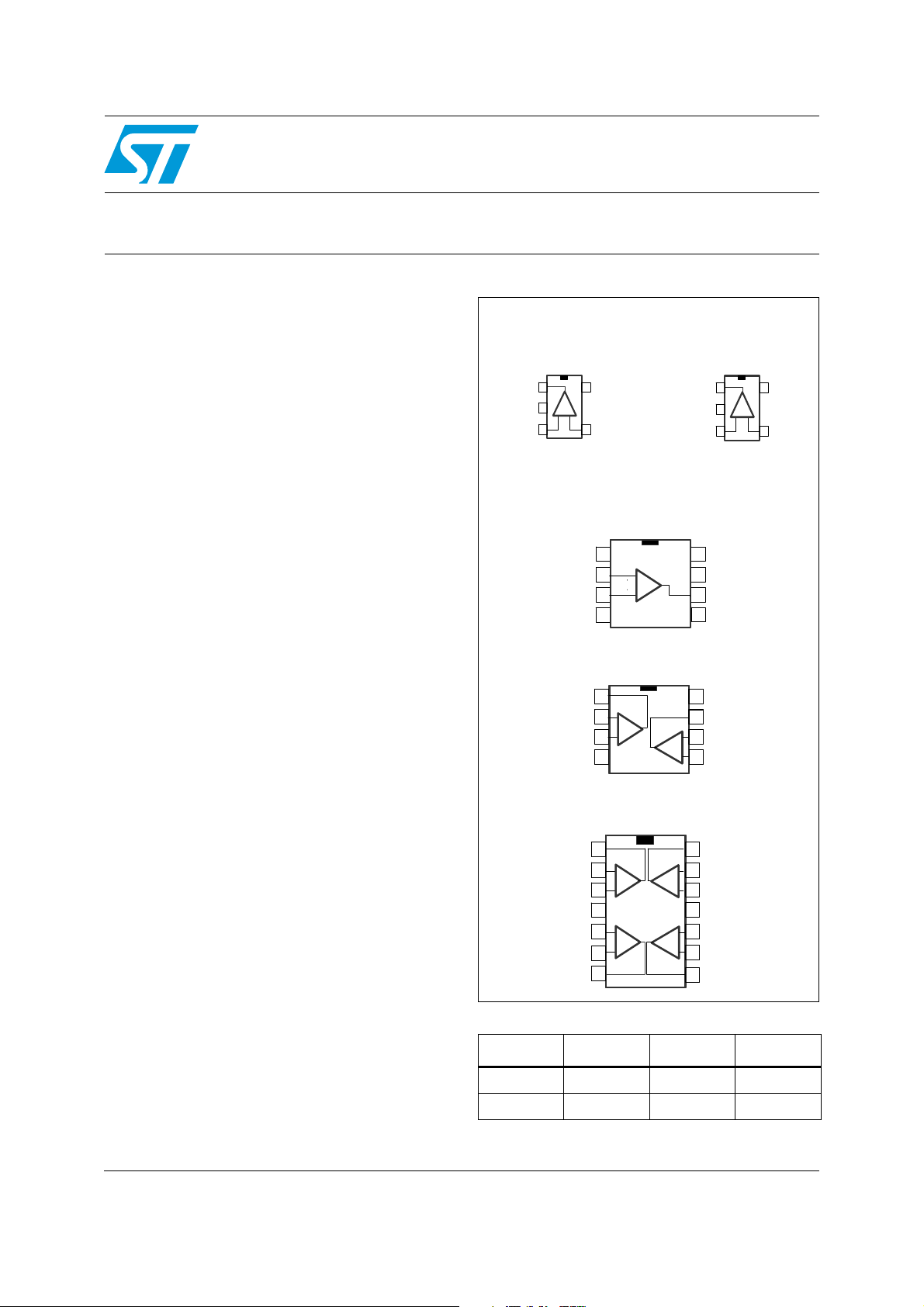
Pin connections (top view)
SOT23-5
Out
1
V
2
CC-
3
In+
TSV911ILT
V
5
CC+
In-
4
Out
V
CC+
In+
TSV911RILT
SO-8 (single)
N.C.
1
_
2
In-
In+
V
CC-
+
3
4
8
7
6
5
MiniSO-8, SO-8, DFN8 2x2 (dual)
Out1
Out1
In1-
In1-
In1+
In1+
V
V
1
1
_
_
2
2
+
+
3
3
4
4
CC-
CC-
8
8
V
V
7
7
Out2
Out2
_
_
In2-
In2-
6
6
+
+
In2+
In2+
5
5
1
2
3
N.C.
V
CC+
Out
N.C.
CC+
CC+
V
5
CC-
In-
4
Description
The TSV91x operational amplifiers offer low
voltage operation and rail-to-rail input and output,
as well as an excellent speed/power consumption
ratio, providing an 8 MHz gain-bandwidth product
while consuming only 1.1 mA maximum at 5 V.
The op-amps are unity gain stable and feature an
ultra-low input bias current.
The devices are ideal for sensor interfaces,
SO-14, TSSOP14
1
1
Out1
Out1
_
_
2
2
In1-
In1-
+
In1+
In1+
V
V
CC+
CC+
In2+
In2+
In2-
In2-
Out2
Out2
+
3
3
4
4
5
5
+
+
_
_
6
6
7
7
14
14
Out4
Out4
_
_
13
13
In4-
In4-
+
+
In4+
In4+
12
12
V
V
11
11
CC-
CC-
10
10
In3+
In3+
+
+
_
_
In3-
In3-
9
9
Out3
Out3
8
8
battery-supplied and portable applications, as
well as active filtering.
March 2012 Doc ID 12584 Rev 8 1/22
This is information on a product in full production.
Table 1. Device summary
Reference Single Dual Quad
TSV91x TSV911 TSV912 TSV914
TSV91xA TSV911A TSV912A TSV914A
www.st.com
22
Absolute maximum ratings and operating conditions TSV91x, TSV91xA
1 Absolute maximum ratings and operating conditions
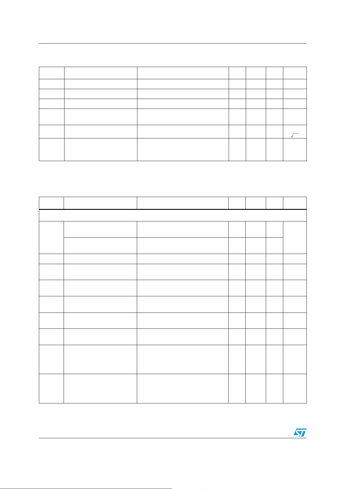
Table 2. Absolute maximum ratings
Symbol Parameter Value Unit
(3)
(4)
(1)
(8)
(2)
(7)
(9)
(5) (6)
(5) (6)
V
CC-
6V
±V
CC
-0.2 to V
+0.2 V
CC+
V
10 mA
250
57
125
°C/W
190
103
100
81
40
39
°C/W
31
32
5kV
400 V
1500
750
V
500
V
CC
V
V
I
in
T
stg
Supply voltage
Differential input voltage
id
Input voltage
in
Input current
Storage temperature -65 to +150 °C
Thermal resistance junction to ambient
SOT23-5
DFN8 2x2
R
thja
SO-8
MiniSO-8
SO-14
TSSOP14
Thermal resistance junction to case
SOT23-5
R
thjc
SO-8
MiniSO-8
SO-14
TSSOP14
T
Maximum junction temperature 150 °C
j
HBM: human body model
MM: machine model
ESD
CDM: charged device model
SOT23-5, SO-8, MiniSO-8
TSSOP14
SO-14
Latch-up immunity 200 mA
1. All voltage values, except differential voltage, are with respect to network ground terminal.
2. Differential voltages are the non-inverting input terminal with respect to the inverting input terminal.
3. VCC-Vin must not exceed 6 V.
4. Input current must be limited by a resistor in series with the inputs.
5. Short-circuits can cause excessive heating and destructive dissipation.
6. R
are typical values.
th
7. Human body model: a 100 pF capacitor is charged to the specified voltage, then discharged through a
1.5kΩ resistor between two pins of the device. This is done for all couples of connected pin combinations
while the other pins are floating.
8. Machine model: a 200 pF capacitor is charged to the specified voltage, then discharged directly between
two pins of the device with no external series resistor (internal resistor < 5 Ω). This is done for all couples of
connected pin combinations while the other pins are floating.
9. Charged device model: all pins and the package are charged together to the specified voltage and then
discharged directly to the ground through only one pin. This is done for all pins.
2/22 Doc ID 12584 Rev 8

TSV91x, TSV91xA Absolute maximum ratings and operating conditions
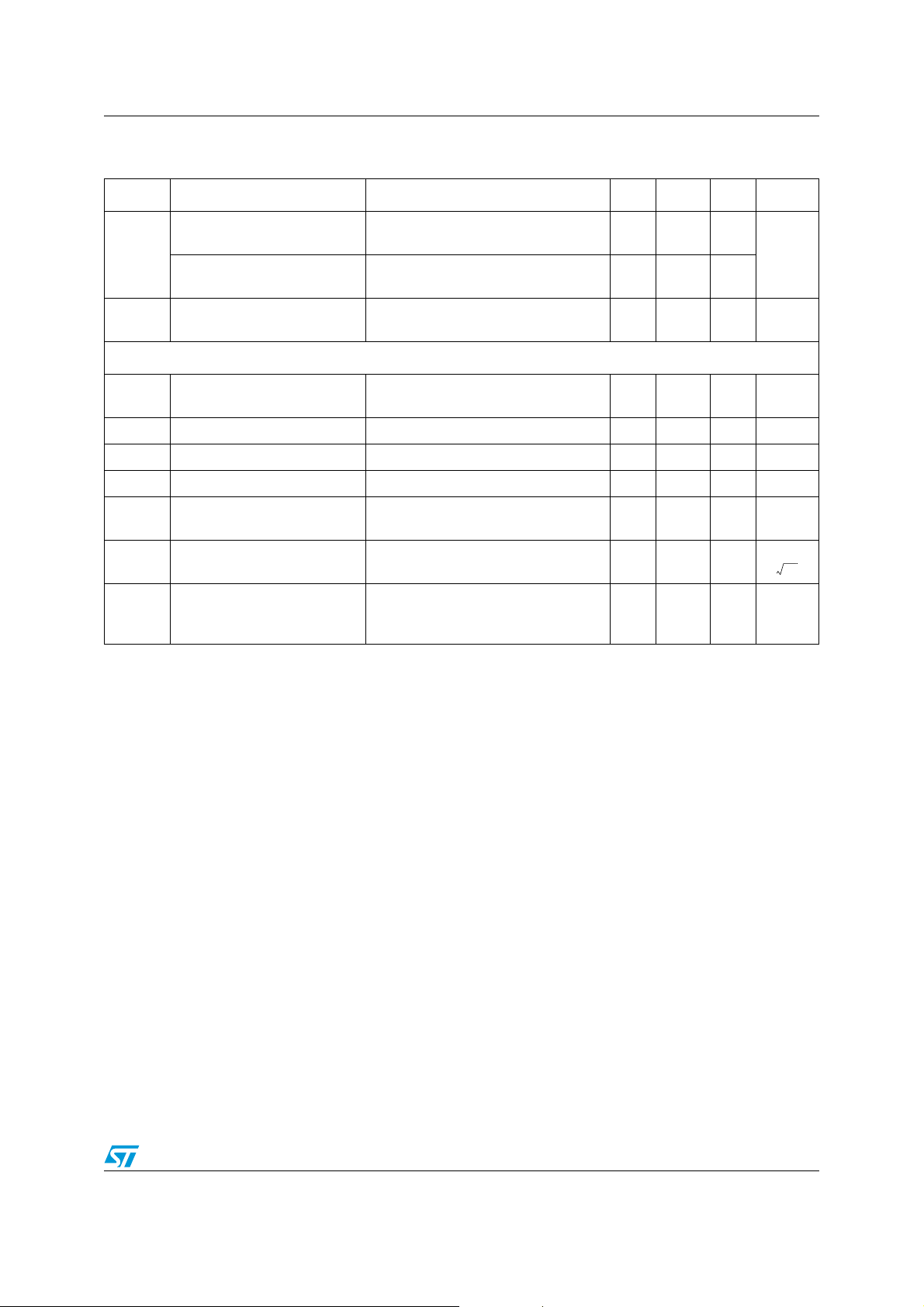
Table 3. Operating conditions
Symbol Parameter Value Unit
Supply voltage
T
V
V
CC
icm
oper
-0.1 to V
CC-
2.5 to 5.5
2.3 to 5.5
CC+
+0.1 V
-40°C < T
0°C < T
< 125°C
op
< 125°C
op
Common mode input voltage range V
Operating free air temperature range -40 to +125 °C
V
Doc ID 12584 Rev 8 3/22
Electrical characteristics TSV91x, TSV91xA
2 Electrical characteristics
Table 4. Electrical characteristics at V
Symbol Parameter Conditions Min. Typ. Max. Unit
DC performance
/2, full temperature range (unless otherwise specified)
to V
CC
= +2.5 V with V
CC+
= 0 V, V
CC-
= VCC/2, RL connected
icm
(1)
Offset voltage
TSV91x
V
io
TSV91xA
Top= 25°C
T
< Top < T
min
T= 25°C
T
< Top < T
min
max
max
0.1 4.5
7.5
1.5
3
mV
DVio/DT Input offset voltage drift 5 μV/°C
I
I
CMR
A
V
CC-VOH
V
I
out
I
CC
Input offset current
io
Input bias current
ib
Common mode rejection ratio
20 log (ΔV
Large signal voltage gain
vd
/ΔVio)
ic
High level output voltage
Low level output voltage
OL
I
sink
I
source
Supply current (per operator)
(2)
(2)
Top= 25°C
T
< Top < T
min
max
Top= 25°C
T
< Top < T
min
0V to 2.5V, V
T
< Top < T
min
= 10kΩ, V
R
L
T
< Top < T
min
=10kΩ
R
L
T
< Top < T
min
max
= 1.25V, Top= 25°C
out
max
= 0.5V to 2V, T= 25°C
out
max
max
RL=600Ω
T
< Top < T
min
R
L
T
min
=10kΩ
< Top < T
max
max
RL=600Ω
< Top < T
T
min
max
Vo = 2.5V, Top= 25°C
< Top < T
T
min
max
Vo = 0V, Top= 25°C
< Top < T
T
min
No load, V
< Top < T
T
min
max
out=VCC
max
/2
58
53
80
75
18
16
18
16
110
100
110
100
75
89
15
40
40
45
150
150
15
40
40
45
150
150
32
35
0.78 1.1
1.1
pA
pA
dB
dB
mV
mV
mA
mA
AC performance
=2kΩ, CL=100pF, f =100kHz,
R
GBP Gain bandwidth product
F
Unity gain frequency RL=2kΩ, CL= 100pF, T
u
φm Phase margin R
G
Gain margin RL=2kΩ, CL= 100pF, T
m
SR Slew rate
L
T
=25°C
op
=2kΩ, CL= 100pF, T
L
RL=2kΩ, CL=100pF, Av=1,
T
=25°C
op
4/22 Doc ID 12584 Rev 8
8MHz
= 25°C 7.2 MHz
op
= 25°C 45 Degrees
op
= 25°C 8 dB
op
4.5 V/μs
TSV91x, TSV91xA Electrical characteristics
Table 4. Electrical characteristics at V
/2, full temperature range (unless otherwise specified)
to V
CC
= +2.5 V with V
CC+
= 0 V, V
CC-
= VCC/2, RL connected
icm
(1)
(continued)
Symbol Parameter Conditions Min. Typ. Max. Unit
e
Equivalent input noise voltage f= 10kHz, T
n
= 25°C 21
op
G=1, f=1kHz, RL=2kΩ, Bw= 22kHz,
THD+e
1. All parameter limits at temperatures other than 25°C are guaranteed by correlation.
2. Guaranteed by design.
Table 5. Electrical characteristics at V
Total harmonic distortion
n
/2, full temperature range (unless otherwise specified)
to V
CC
T
op
V
out
=25°C, V
=1.1V
icm
pp
= +3.3 V with V
CC+
=(VCC+1)/2,
= 0 V, V
CC-
0.001 %
= VCC/2, RL connected
icm
(1)
Symbol Parameter Conditions Min. Typ. Max. Unit
DC performance
V
DV
I
I
CMR
A
V
CC-VOH
V
I
out
I
CC
Offset voltage
TSV91x
io
TSV91xA
Input offset voltage drift 5 μV/°C
io
Input offset current
io
Input bias current
ib
(2)
(2)
Common mode rejection ratio
20 log (ΔV
Large signal voltage gain
vd
/ΔVio)
ic
High level output voltage
Low level output voltage
OL
I
sink
I
source
Supply current (per operator)
Top= 25°C
T
< Top < T
min
T
= 25°C
op
T
< Top < T
min
Top= 25°C
T
< Top < T
min
Top= 25°C
< Top < T
T
min
0V to 3.3V, V
< Top < T
T
min
=10kΩ, V
R
L
T
< Top < T
min
=10kΩ
R
L
T
< Top < T
min
RL=600Ω
< Top < T
T
min
=10kΩ
R
L
T
< Top < T
min
RL=600Ω
T
< Top < T
min
Vo = 3.3V, T
< Top < T
T
min
Vo = 0V, T
T
min
No load, V
T
min
op
< Top < T
out=VCC
< Top < T
max
max
max
max
= 1.65V
out
max
= 0.5V to 2.8V, T=25°C
out
max
max
max
max
max
= 25°C
op
max
= 25°C
max
/2
max
60
55
80
75
18
16
18
16
0.1 4.5
7.5
1.5
3
110
100
110
100
78
90
15
40
40
45
150
150
15
40
40
45
150
150
32
35
0.8 1.1
1.1
AC performance
nV
-----------Hz
mV
pA
pA
dB
dB
mV
mV
mA
mA
GBP Gain bandwidth product
=2kΩ, CL= 100pF, f = 100kHz,
R
T
op
L
=25°C
8MHz
Doc ID 12584 Rev 8 5/22
Electrical characteristics TSV91x, TSV91xA
Table 5. Electrical characteristics at V
/2, full temperature range (unless otherwise specified)
to V
CC
= +3.3 V with V
CC+
= 0 V, V
CC-
= VCC/2, RL connected
icm
(1)
(continued)
Symbol Parameter Conditions Min. Typ. Max. Unit
F
Unity gain frequency RL= 2kΩ, CL=100pF, T
u
φm Phase margin R
G
Gain margin RL=2kΩ, CL=100pF, T
m
SR Slew rate
e
Equivalent input noise voltage f= 10kHz, Top= 25°C 21
n
=2kΩ, CL=100pF, T
L
=2kΩ, CL= 100pF, Av=1,
R
L
=25°C
T
op
= 25°C 7.2 MHz
op
= 25°C 45 Degrees
op
= 25°C 8 dB
op
4.5 V/μs
G=1, f=1kHz, RL=2kΩ, BW= 22kHz,
THD+e
1. All parameter limits at temperatures other than 25°C are guaranteed by correlation.
2. Guaranteed by design.
Table 6. Electrical characteristics at V
Total harmonic distortion
n
/2, full temperature range (unless otherwise specified)
V
CC
V
=(VCC+1)/2, V
icm
=25°C
T
op
CC+
=1.9Vpp,
out
= +5 V with V
CC-
= 0 V, V
icm
0.0007 %
= VCC/2, RL connected to
(1)
Symbol Parameter Conditions Min. Typ. Max. Unit
DC performance
nV
-----------Hz
V
DV
I
I
CMR
SVR
A
V
CC-VOH
V
Offset voltage
TSV91x
io
TSV91xA
Input offset voltage drift 5 - μV/°C
io
Input offset current
io
Input bias current
ib
(2)
(2)
Common mode rejection ratio
20 log (ΔV
/ΔVio)
ic
Supply voltage rejection ratio
20 log (ΔV
Large signal voltage gain
vd
CC
/ΔVio)
High level output voltage
Low level output voltage
OL
Top= 25°C
T
< Top < T
min
T
op
T
min
= 25°C
< Top < T
max
max
Top= 25°C
T
< Top < T
min
max
Top= 25°C
T
< Top < T
min
0V to 5V, V
< Top < T
T
min
V
= 2.5 to 5V 70 86 - dB
CC
R
=10kΩ, V
L
T
< Top < T
min
=10kΩ
R
L
< Top < T
T
min
max
= 2.5V
out
max
= 0.5V to 4.5V, T= 25°C
out
max
max
62
58
80
75
RL=600Ω
T
< Top < T
min
R
L
T
min
=10kΩ
< Top < T
max
max
RL=600Ω
< Top < T
T
min
max
0.1 4.5
110
110
82
91
15
45
15
45
7.5
mV
1.5
3
100
100
pA
pA
-dB
-dB
40
40
150
mV
150
40
40
150
mV
150
6/22 Doc ID 12584 Rev 8
TSV91x, TSV91xA Electrical characteristics
Table 6. Electrical characteristics at V
/2, full temperature range (unless otherwise specified)
V
CC
= +5 V with V
CC+
CC-
= 0 V, V
= VCC/2, RL connected to
icm
(1)
(continued)
Symbol Parameter Conditions Min. Typ. Max. Unit
I
I
I
sink
out
I
source
Supply current (per operator)
CC
Vo = 5V, T
< Top < T
T
min
Vo = 0V, T
T
< Top < T
min
No load, V
T
< Top < T
min
=25°C
op
= 25°C
op
out
max
max
= 2.5V
max
18
16
18
16
32
35
0.82 1.1
1.1
AC performance
GBP Gain bandwidth product
F
Unity gain frequency RL = 2kΩ, CL=100pF, T
u
φm Phase margin R
G
Gain margin RL = 2kΩ, CL=100pF, T
m
SR Slew rate
e
Equivalent input noise voltage
n
L
=25°C
T
op
op
= 2kΩ, CL=100pF, T
L
=2kΩ, CL= 100pF, AV=1,
R
L
=25°C
T
op
f=1kHz, T= 25°C
f=10kHz, T
=25°C
op
= 25°C 7.5 MHz
= 25°C 45 Degrees
op
= 25°C 8 dB
op
8MHz
4.5 V/μs
27
21
=2kΩ, CL= 100pF, f = 100kHz,
R
G=1, f=1kHz, RL=2kΩ, Bw= 22kHz,
THD+e
1. All parameter limits at temperatures other than 25°C are guaranteed by correlation.
2. Guaranteed by design.
Total harmonic distortion
n
T
op
V
out
=25°C, V
=3.6V
pp
=(VCC+1)/2,
icm
0.0004 %
mA
mA
nV
-----------Hz
Doc ID 12584 Rev 8 7/22
 Loading...