

Low Consumption Voltage and Current
Controller for Battery Chargers and Adaptors
■ Constant voltage and constant current
control
■ Low con sumpti on
■ Low voltage operation
■ Low external component count
■ Curre nt sink ou tput stage
■ Easy compensation
■ High ac mains voltage rejection
■ 2kV ESD protection (HBM)
Voltage Reference:
■ Fixed output voltage reference 1.25V
■ 0.5% and 1% Voltage precision
DESCRIPTION
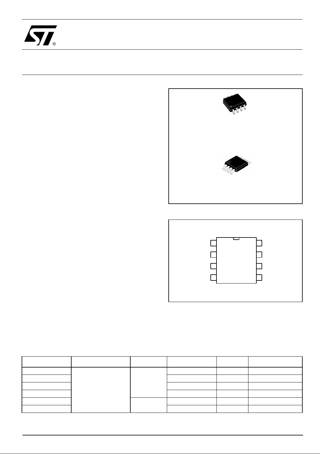
TSM1014
D
SO-8
(Plastic Package)
S
MiniSO-8
(Plastic Micropackage)
TSM1014 is a highly integrated solution for SMPS
PIN CONNECTIONS (top view)
applications requiring CV (cons tant voltage) and
CC (constant current) mode.
TSM1014 integrates one voltage reference and
1
VccVref
8
two operational amplifiers.
The voltage reference combined with one
operational amplifier makes it an ideal voltage
controller. The other operational amplifier,
combined with few external resistors and the
Cc-
3
Cc+
45
Cv- Cv Out
Cc Out 7
Gnd
6
2
voltage reference, can be used as a current
limiter.
APPLICATIONS
■ Adapters
■ Battery chargers
ORDER CODES
Part Number Temperature Range Package Packaging VRef (%) Marking
TSM1014ID
TSM1014IDT Tape & Reel 1 M1014
TSM1014AID Tube 0.5 M1014A
TSM1014AIDT Tape & Reel 0.5 M1014A
TSM1014IST
TSM1014AIST Tape & Reel 0.5 M809
-40 to 105°C
SO-8
mini SO-8
Tube 1 M1014
Tape & Reel 1 M808
July 2004 Revision 1 1/10
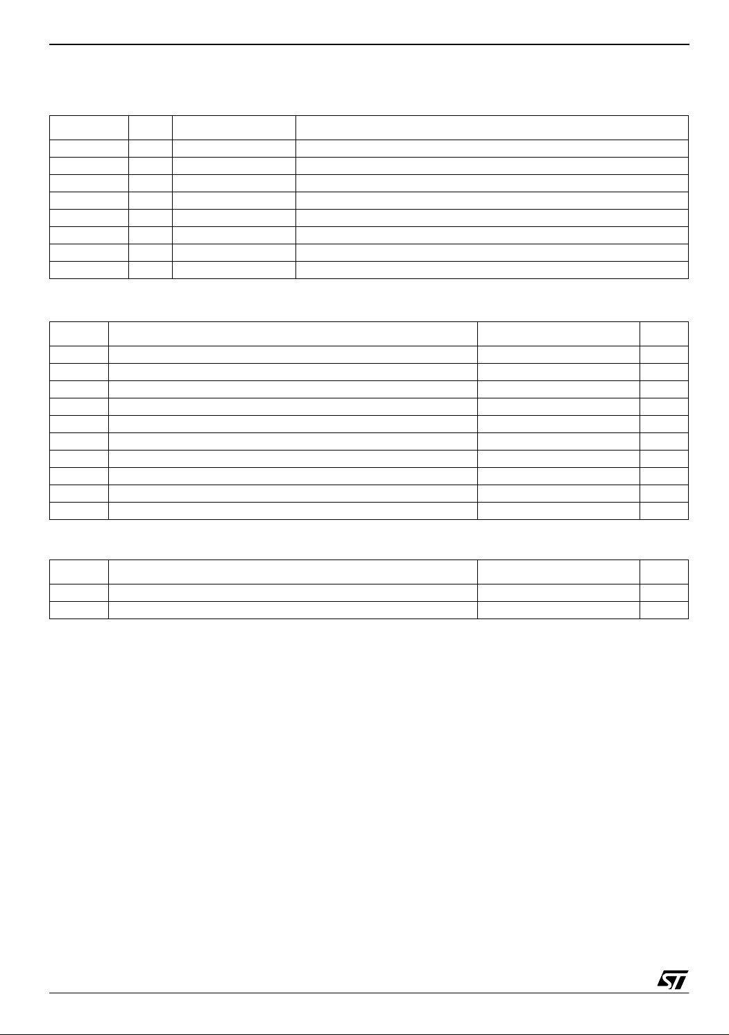
TSM1014 Pin Descriptions
1 Pin Descriptions
The table below gives the pin descriptions for both SO8 & MiniSO8 packages.
Name Pin # Type Function
VRef 1 Analog Output Voltage Reference
CC- 2 Analog Input Input pin of the operational amplifier
CC+ 3 Analog Input Input pin of the operational amplifier
CV- 4 Analog Input Input pin of the operational amplifier
CVOUT 5 Analog Output Output of the operational amplifier
Gnd 6 Power Supply Ground Line. 0V Reference For All Voltages
CCOUT 7 Analog Output Output of the operational amplifier
Vcc 8 Power Supply Power supply line.
2 Absolute Maximum Ratings
Symbol DC Supply Voltage Value Unit
Vcc DC Supply Voltage (50mA =< Icc) -0.3V to Vz V
Vi Input Voltage -0.3 to Vcc V
PT Power dissipation W
Toper Operational temperature 0 to 105 °C
Tstg Storage temperature -55 to 150 °C
Tj Junction temperature 150 °C
Iref Voltage reference output current 2.5 mA
ESD Electrostatic Discharge 2 kV
Rthja Thermal Resistance Junction to Ambient Mini SO8 package 180 °C/W
Rthja Thermal Resistance Junction to Ambient SO8 package 175 °C/W
3 Operating Cond itions
Symbol Parameter Value Unit
Vcc DC Supply Conditions 4.5 to Vz V
Toper Operational temperature -40 to 105 °C
2/10
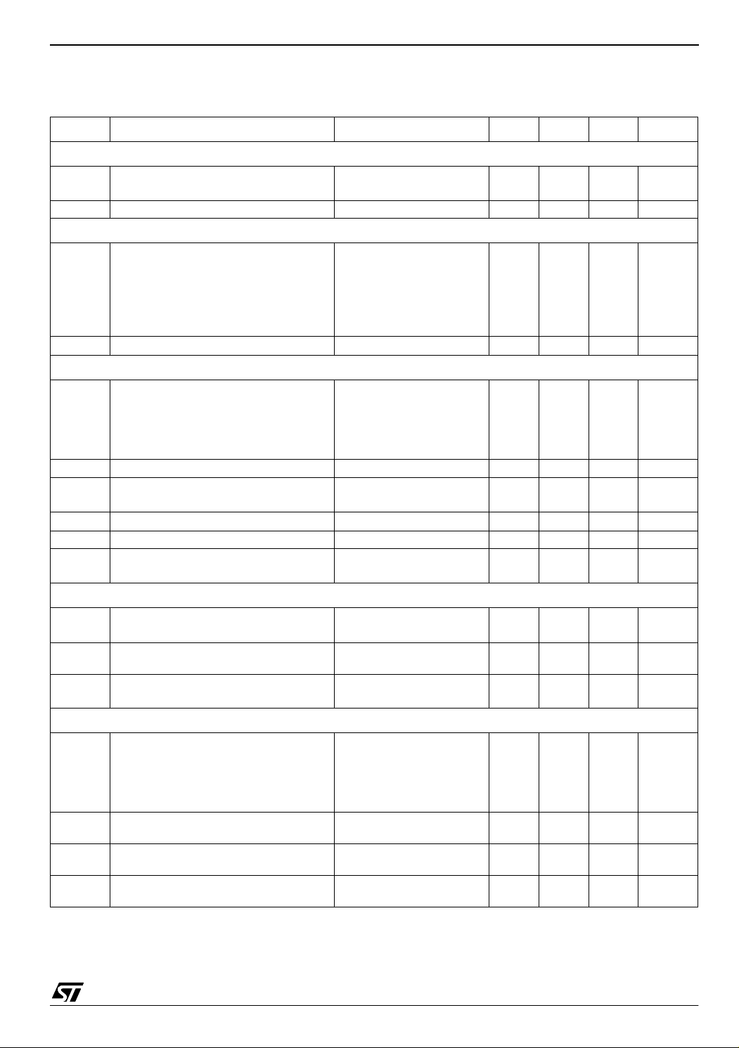
Electrical Characteristics TSM1014
4 Electrical Characteristics
Tamb = 25°C and Vcc = +18V (unless otherwise specified)
Symbol Parameter Test Condition Min Typ Max Unit
Total Current Consumption
Total Supply Current, excluding current
Icc
in Voltage Reference
1
.
Vz Vcc clamp voltage Icc = 50mA 28 V
Operator 1: Op-amp with non-inverting input connected to the internal VRef
Input Offset Voltage + Voltage reference
TSM1014
VRef+V
io
TSM1014A
Vcc = 18V, no load
Tmin. < Tamb < Tmax.
T
= 25°C
amb
T
≤ T
amb
= 25°C
≤ T
amb
≤ T
≤ T
max.
max.
min.
T
amb
T
min.
100 180 µA
1.251
1.25
1.266
1.279
1.258
1.267
V
DV
Input Offset Voltage Drift
io
7
µV/°C
Operator 2
Input Offset Voltage
V
io
DV
I
ib
SVR
TSM1014
TSM1014A
Input Offset Voltage Drift
io
Input Bias Current T
Supply Voltage Rejection Ration V
T
= 25°C
amb
T
≤ T
min.
T
T
T
amb
= 25°C
amb
≤ T
min.
amb
= 25°C
amb
≤ T
min.
amb
= 4.5V to 28V
CC
≤ T
≤ T
≤ T
max.
max.
max.
1
0.5
7
20
50
4
5
2
3
150
200
mV
µV/°C
nA
65 100 dB
Vicm Input Common Mode Voltage Range 0 Vcc-1.5 V
CMR
Common Mode Rejection Ratio T
T
amb
min.
= 25°C
≤ T
amb
≤ T
max.
70
60
85
dB
Output stage
Gm
Vol
Ios
Transconduction Gain. Sink Current
2
Only
Low output voltage at 5 mA sinking cur-
rent
Output Short Circuit Current. Output to
(Vcc-0.6V). Sink Current Only
T
T
T
T
T
amb
min.
min.
amb
min.
= 25°C
≤ T
amb
≤ T
amb
= 25°C
≤ T
amb
≤ T
≤ T
≤ T
max.
max.
max.
0.5
6
5
1
1
mA/mV
250 400 mV
10
mA
Voltage reference
Reference Input Voltage
TSM1014 1% precision
V
Ref
TSM1014A 0.5% precision
∆V
RegLine
RegLoad
1) Test conditions: pin 2 and 6 connected t o GND, pin 4 and 5 co nnected to 1.2 5V , pin 3 connected to 200mV.
2) The curr ent depends on the voltage dif f erence between the negati ve and the positive inputs of the amplifier. If the voltage on the minus
input is 1mV higher than the positive amplifier, the sinking current at the output OUT will be increased by Gm*1mA.
Reference Input Voltage Deviation Over
Ref
Temperature Range
Reference input voltage deviation over
Vcc range.
Reference input voltage deviation over
output current.
T
= 25°C
amb
T
≤ T
amb
= 25°C
≤ T
amb
≤ T
amb
≤ T
≤ T
≤ T
max.
max.
max.
min.
T
amb
T
min.
T
min.
Iload = 1mA
Vcc = 18V,
0 < Iload < 2.5mA
1.238
1.225
1.244
1.237
1.25
1.262
1.273
1.25
1.256
1.261
20 30 mV
20 mV
10 mV
V
3/10
 Loading...