

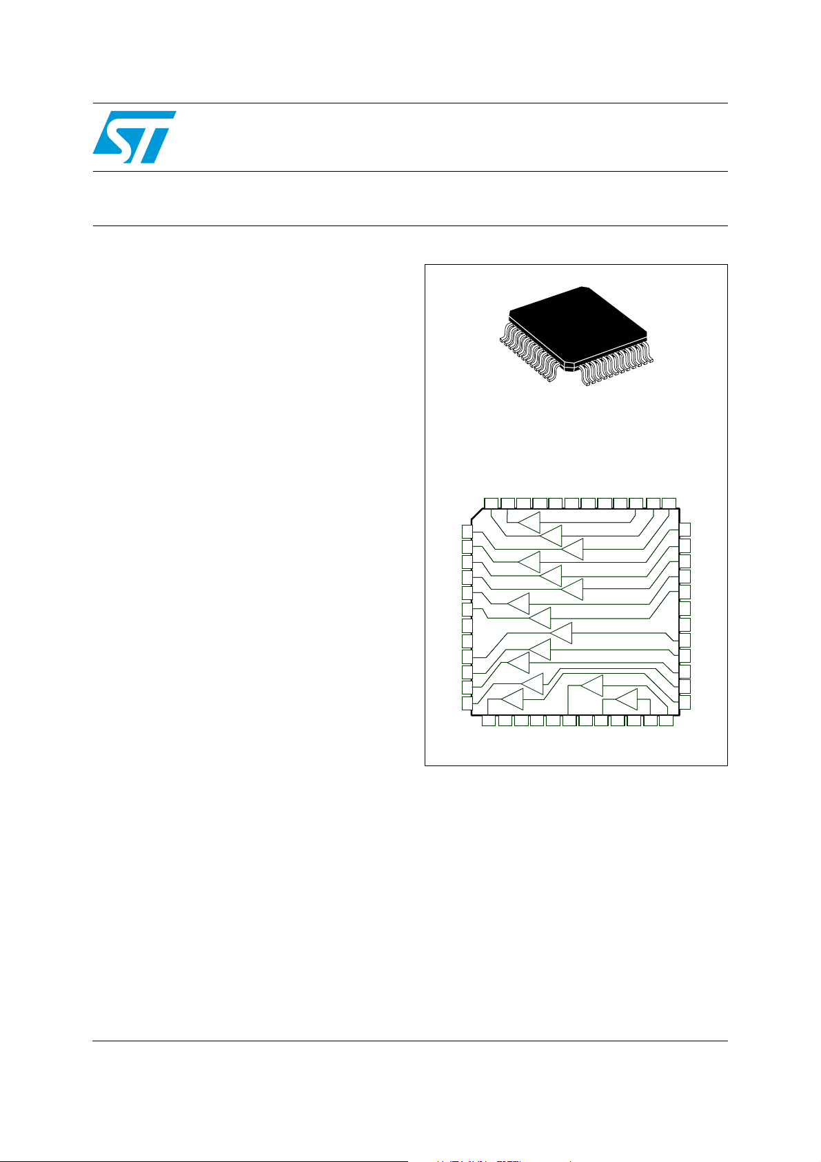
14 + 1 channel buffers for TFT-LCD panels
Features
■ Wide supply voltage: 5.5 V to 16.8 V
■ Low operating current: 6 mA typical at 25° C
■ Gain bandwidth product: 1 MHz
■ High current com amplifier: ±100 mA output
current
■ Industrial temperature range: -40° C to +85° C
■ Small package: TQFP48
■ Automotive qualification
TSL1014
7 x 7mm TQFP48
Pin connections (top view)
Application
■ TFT liquid crystal display (LCD)
Description
The TSL1014 is composed of 14 + 1 channel
buffers which are used to buffer the reference
voltage for gamma correction in thin film transistor
(TFT) liquid crystal displays (LCD).
One "COM" amplifier is able to deliver high output
current value, up to ±100mA. Amplifiers A and B
feature positive single supply inputs for common
mode voltage behavior. The amplifiers C to N
inclusive, and the COM amplifier, feature negative
single-supply inputs and are dedicated to the
highest and lowest gamma voltages.
The TSL1014 is fully characterized and
guaranteed over a wide industrial temperature
range (-40 to +85° C).
VSSVDD
VSSVDD
VSSVD D
VSSVD D
47
48 44 43 42 41 40 39 38 3746 45
47
48 44 43 42 41 40 39 38 3746 45
Com
Com
L
L
I
I
H
H
F
F
E
E
D
D
C
C
13 14 15 16 17 18 19 20 21 22
13 14 15 16 17 18 19 20 21 22
VDD VSS
VDD VSS
VSS
VSS
VDD
VDD
1
1
2
2
3
3
4
4
5
5
6
6
7
7
8
8
9
9
10
10
11
11
12
12
36
23 24
23 24
36
35
35
34
34
33
33
32
32
VSS
VSS
31
31
VDD
VDD
30
30
29
29
28
28
27
27
26
26
25
25
N
N
M
M
K
K
J
J
G
G
B
B
A
A
VDD
VDD
VSS
VSS
May 2009 Doc ID 11528 Rev 6 1/17
www.st.com
17
Absolute maximum ratings and operating conditions TSL1014
1 Absolute maximum ratings and operating conditions
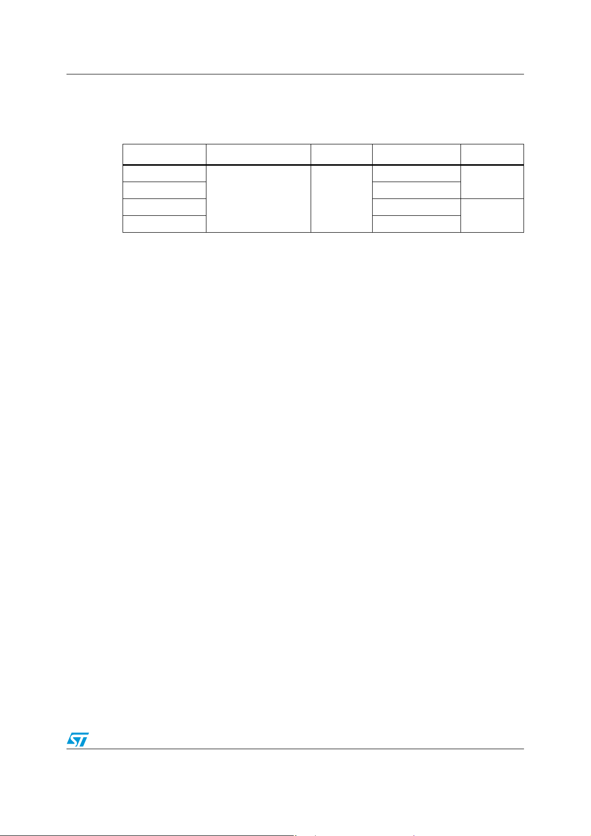
Table 1. Absolute maximum ratings
Symbol Parameter Value Unit
V
V
I
OUT
I
SC
P
R
THJA
T
LEAD
T
STG
T
ESD
1. PD is calculated with T
2. Human body model: a 100 pF capacitor is charged to the specified voltage, then discharged through a
1.5 kΩ resistor between two pins of the device. This is done for all couples of connected pin combinations
Supply voltage (VDD-VSS)18V
CC
Input voltage V
IN
Output current (A to N buffers)
Output current (Com buffer)
Short circuit current (A to N buffers)
Short circuit current (Com buffer)
Power dissipation
D
(1)
for TQFP48
-0.5V to V
SS
+0.5V V
DD
30
100
±120
±300
1470 mW
Thermal resistance junction to ambient for TQFP48 85 °C/W
Lead temperature (soldering 10 seconds) 260 °C
Storage temperature -65 to +150 °C
Junction temperature 150 °C
J
Human body model (HBM)
(2)
(3)
Charged device model (CDM)
= 25° C, TJ = 150° C and R
amb
(4)
= 85° C/W for the TQFP48 package.
THJA
2000
200
1500
while the other pins are floating.
3. Machine model: a 200 pF capacitor is charged to the specified voltage, then discharged directly between
two pins of the device with no external series resistor (internal resistor < 5 Ω). This is done for all couples of
connected pin combinations while the other pins are floating.
4. Charged device model: all pins and package are charged together to the specified voltage and then
discharged directly to the ground through only one pin.
mA
mA
VMachine model (MM)
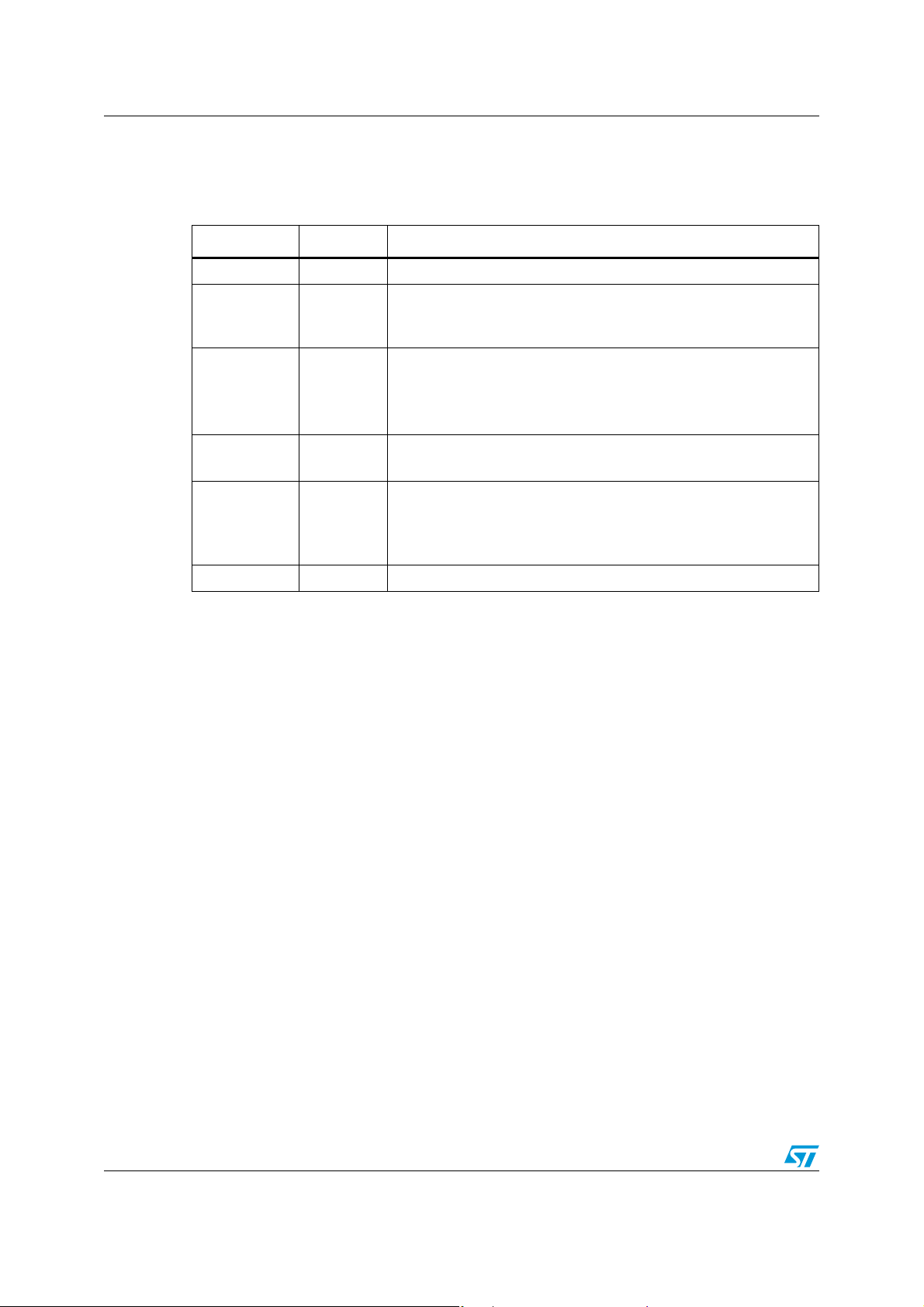
Table 2. Operating conditions
Symbol Parameter Value Unit
T
V
amb
Supply voltage (VDD-VSS) 5.5 to 16.8 V
CC
Ambient temperature -40 to +85 °C
Input voltage (Buffers A & B) V
V
IN
Input voltage (Buffers C to N + COM) V
2/17 Doc ID 11528 Rev 6
+1.5V to V
SS
to V
SS
DD
-1.5V
DD
V
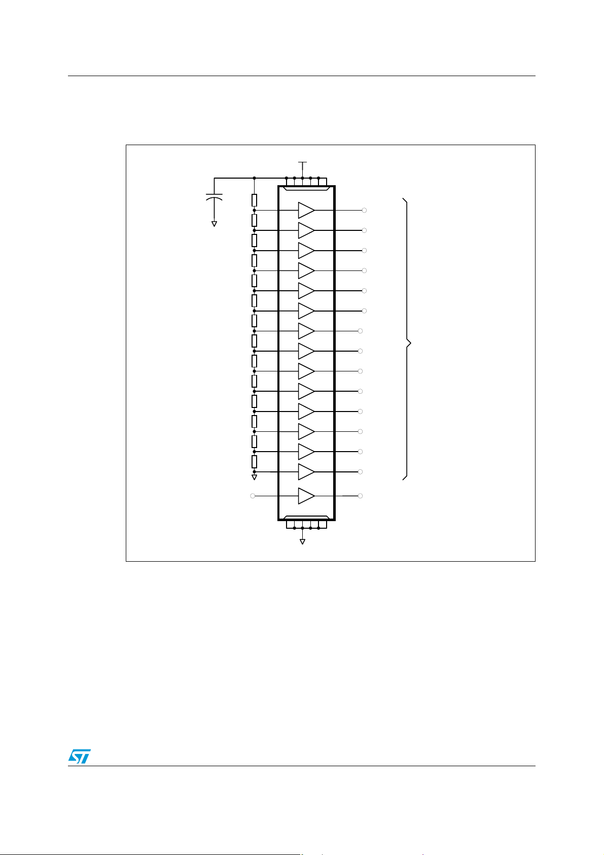
TSL1014 Typical application schematics
2 Typical application schematics
Figure 1. A typical application schematic for the TSL1014
Vcc
15
22
8
30
7
192021
VDD
A
B
C
D
E
F
G
H
I
J
K
L
M
N
VSS
31
434445
COM
Gamma 13
18
Gamma 12
13
Gamma 11
12
Gamma 10
11
Gamma 9
10
Gamma 8
9
Gamma 7
6
Gamma 6
5
Gamma 5
4
Gamma 4
3
Gamma 3
2
Gamma 2
1
Gamma 1
48
Gamma 0
47
VCOM
46
To colunm driver
Cs
+
10uF
Gnd
Com Ref. Voltage
R1
23
R2
24
R3
25
R4
26
R5
27
R6
28
R7
29
R8
32
R9
33
R10
34
R11
35
R12
36
R13
37
R14
38
Gnd
39
Gnd
Note that:
● Amplifiers A & B have their input voltage in the range V
+1.5 V to VDD. This is why
SS
they must be used for high level gamma correction voltages.
● Amplifiers C to N have their input voltage in the range V
to VDD-1.5 V. This is why
SS
they must be used for medium-to-low level gamma correction voltages.
● Amplifier COM has its input voltage range from V
Doc ID 11528 Rev 6 3/17
to VDD-1.5 V.
SS
Electrical characteristics TSL1014
3 Electrical characteristics
Table 3. Electrical characteristics for TSL1014IF/TSL1014IFT
T
=25°C, VDD=+5V, VSS=-5V, RL=10kΩ, CL=10pF
amb
(unless otherwise specified)
Symbol Parameter Test conditions Min. Typ. Max. Unit
V
ΔV
R
C
V
V
I
OUT
Input offset voltage V
IO
Input offset voltage drift T
IO
I
Input bias current
IB
Input impedance 1 GΩ
IN
Input capacitance 1.35 pF
IN
Output voltage low
OL
Output voltage high
OH
Output current
PSRR Power supply rejection ratio V
I
SR
Supply current No load 6 8.4 mA
CC
Slew rate
(rising & falling edge)
Settling time Settling to 0.1%, V
t
s
BW Bandwidth at -3dB R
G
Phase margin RL=10 kΩ, CL=10 pF 60 degrees
m
Channel separation f=1 MHz 75 dB
C
s
= 0 V 12 mV
ICM
< T
Min
V
ICM
V
ICM
I
OUT
Buffers C to L
Buffers M, N & COM
I
OUT
buffers (A & B)
< T
amb
Max
= 0V, buffers A & B
= 0V, buffers C to N & COM
=-5mA
= 5 mA for positive single-supply
5 μV/°C
140
70
-4.85
-4.92
-4.80
-4.85
4.82 4.87 V
(A to N buffers) ±30
Com buffer ±100
= 6.5 to 15.5 V 80 100 dB
CC
-4 V < V
20% to 80%
=10 kΩ, CL=10 pF 2 MHz
L
OUT
< +4 V
1V/μs
=2V step 5 μs
OUT
nA
V
mA
Note: Limits are 100% production tested at 25° C. Behavior at the temperature range limits is
guaranteed through correlation and by design.
4/17 Doc ID 11528 Rev 6
TSL1014 Electrical characteristics
Table 4. Electrical characteristics for TSL1014IYF/TSL1014IYFT (automotive grade)
=25°C, VDD=+5V, VSS=-5V, RL=10kΩ, CL=10pF
T
amb
(unless otherwise specified)
Symbol Parameter Test conditions Min. Typ. Max. Unit
V
= 0 V
V
ΔV
R
C
V
V
I
OUT
Input offset voltage
IO
Input offset voltage drift T
IO
I
Input bias current
IB
Input impedance 1 GΩ
IN
Input capacitance 1.35 pF
IN
Output voltage low
OL
Output voltage high
OH
Output current
PSRR Power supply rejection ratio
I
SR
Supply current
CC
Slew rate
(rising & falling edge)
Settling time Settling to 0.1%, V
t
s
BW Bandwidth at -3dB R
G
Phase margin RL=10 kΩ, CL=10 pF 60 degrees
m
Channel separation f=1 MHz 75 dB
C
s
ICM
T
< T
Min
< T
Min
V
ICM
T
< T
Min
V
ICM
T
< T
Min
I
OUT
Buffers C to L
< T
T
Min
Buffers M, N & COM
T
< T
Min
I
OUT
buffers (A & B)
< T
T
Min
< T
amb
Max
< T
amb
Max
= 0 V, buffers A & B
< T
amb
Max
= 0 V, buffers C to N & COM
< T
amb
Max
=-5mA
< T
amb
Max
< T
amb
Max
= 5 mA for positive single-supply
< T
amb
Max
5 μV/°C
-4.85
-4.92
4.82
4.87 V
4.80
12
140
280
70
140
-4.80
-4.76
-4.85
-4.83
(A to N buffers) ±30
Com buffer ±100
= 6.5 to 15.5 V
V
CC
T
Min
< T
amb
< T
Max
No load
T
< T
Min
-4V < V
amb
OUT
< T
Max
< +4 V
20% to 80%
=2V step 5 μs
OUT
=10 kΩ, CL=10 pF 2 MHz
L
100
80
68.4
9
1V/μs
mV
nA
V
mA
dB
mA
Note: Limits are 100% production tested at 25° C. Behavior at the temperature range limits is
guaranteed through correlation and by design.
Doc ID 11528 Rev 6 5/17
Electrical characteristics TSL1014
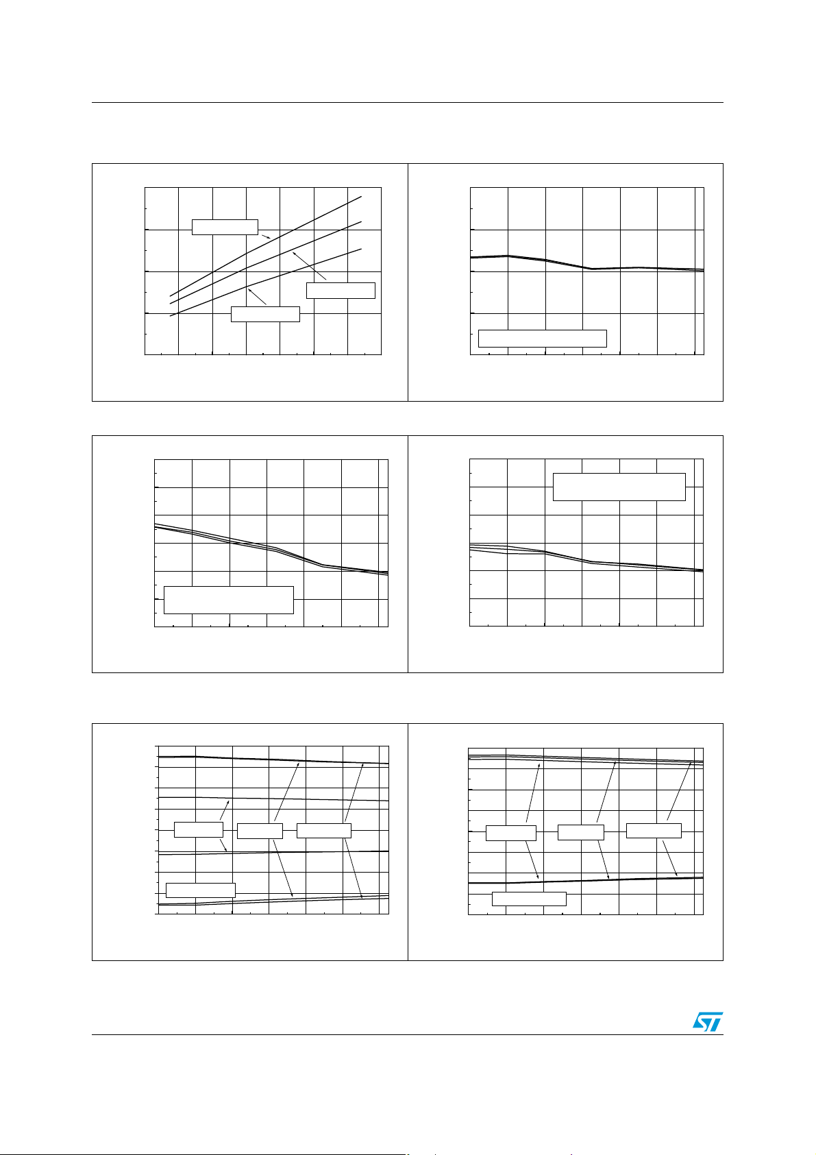
Figure 2. Supply current vs. supply voltage
for various temperatures
8
7
6
Tamb=-40°C
Figure 3. Output offset voltage (eq. VIO) vs.
temperature
1.0
0.5
0.0
Tamb=+25°C
Current consump tion (mA)
5
Tamb=+85°C
Output offset voltage (mV)
-0.5
VCC = +5.5V, +10V, +16.8V
4
4 6 8 1012141618
Sup ply v olta ge (V)
-1.0
-40-20 0 20406080
Ambient temperature (°C)
Figure 4. Input current (IIB) vs. temperature Figure 5. Input current (IIB) vs. temperature
120
100
80
120
100
Buffers C to COM
VCC = +5.5V, +10V, +16.8V
80
60
40
Input bias current (nA)
Buffers A & B
20
VCC = +5.5V, +10V, +16.8V
0
-40-20 0 20406080
Ambient Temperature (°C)
Figure 6. Output current capability vs.
temperature
200
150
100
50
VCC=5.5V
0
-50
Output current (mA)
-100
Buffers A & B
-150
-200
-40-20 0 20406080
VCC=10V
Ambient Temperature (°C)
VCC=16.8V
60
40
Input bias current (nA)
20
0
-40-20 0 20406080
Ambient Temperature (°C)
Figure 7. Output current capability vs.
temperature
80
60
40
20
0
VCC=5.5V
-20
Output current (mA)
VCC=10V
-40
-60
-80
Buffers C to N
-40-200 20406080
Ambient Tem perature (°C)
VCC=16.8V
6/17 Doc ID 11528 Rev 6
TSL1014 Electrical characteristics
Figure 8. Output current capability vs.
temperature
250
200
150
100
50
VCC=5.5V
0
VCC=10V, 16.8V
-50
Output current (mA)
-100
-150
Buffer COM
-200
-250
-40-20 0 20406080
Ambient Temperature (°C)
Figure 10. Low level voltage drop vs.
temperature
200
VCC=16.8V
150
Figure 9. High level voltage drop vs.
temperature
250
VCC = 5.5V
200
150
100
High level voltage drop (mV)
VCC = 16.8V
VCC = 10V
50
Buffers A & B
Iout = 5m A
0
-40-20 0 20406080
Ambient Temperature (°C)
Figure 11. Low level voltage drop vs.
temperature
200
150
VCC=10V
VCC=16.8V
100
Low level voltage drop (mV)
50
Buffers C to L
Iout= 5m A
0
-40-20 0 20406080
VCC=10V
Ambient Temperature (°C)
Figure 12. Voltage output high (VOH) vs.
output current - Buffers A & B
5.5
5.0
4.5
High level output voltage (V)
4.0
Buffers A & B
VCC = 5.5V
3.5
0 5 10 15 20 25 30
T
=+25°C
AMB
Output current (mA)
T
AMB
VCC=5.5V
T
=-40°C
AMB
=+85°C
100
Low level voltage drop (mV)
50
Buffers M, N and COM
Iout=5m A
0
-40-20 0 20406080
Ambient Temperature (°C)
VCC=5.5V
Figure 13. Voltage output high (VOH) vs.
output current - Buffers A & B
10.0
9.8
9.6
9.4
High level output voltage (V)
9.2
Buffers A & B
VCC = 10V
9.0
0 5 10 15 20 25 30
T
AMB
Outpu t current (m A)
=+85°C
T
=-40°C
AMB
T
=+25°C
AMB
Doc ID 11528 Rev 6 7/17

Electrical characteristics TSL1014
Figure 14. Voltage output high (VOH) vs.
output current - Buffers A & B
16.8
T
16.6
16.4
T
=+85°C
High level output voltage (V)
16.2
Buffers A & B
VCC = 16.8 V
16.0
0 5 10 15 20 25 30
AMB
AMB
=-40°C
T
AMB
=+25°C
Outpu t current (m A)
Figure 16. Voltage output low (VOL) vs. output
current - Buffers C to L
1.2
1.0
0.8
0.6
T
AMB
=+85°C
Buffers C to L
VCC = 10V
T
=+25°C
AMB
Figure 15. Voltage output low (VOL) vs. output
current - Buffers C to L
1.2
1.0
T
AMB
=+85°C
Buffers C to L
VCC = 5.5V
0.8
Low level output voltage (V)
0.6
0.4
T
AMB
=-40°C
T
AMB
=+25°C
0.2
0.0
-30 -25 -2 0 -15 -10 -5 0
Output current (mA)
Figure 17. Voltage output low (VOL) vs. output
current - Buffers C to L
1.2
Buffers C to L
1.0
0.8
0.6
T
AMB
=+85°C
VCC = 16.8V
T
=+25°C
AMB
0.4
T
=-40°C
Low level output voltage (V)
AMB
0.2
0.0
-30 -25 -20 -15 -10 -5 0
Output current (mA)
Figure 18. Voltage output low (VOL) vs. output
current - Buffers M, N & COM
1.6
Buffers M, N & COM
VCC = 5.5V
1.2
0.8
Low level output voltage (V)
0.4
0.0
-50 -40 -30 -20 -10 0
T
AMB
T
=+85°C
AMB
=-40°C
Output current (mA)
T
AMB
=+25°C
0.4
Low level output voltage (V)
T
=-40°C
AMB
0.2
0.0
-30-25-20-15-10 -5 0
Output current (mA)
Figure 19. Voltage output low (VOL) vs. output
current - Buffers M, N & COM
2.0
Buffers M, N & COM
T
=+85°C
1.5
AMB
1.0
Low level output voltage (V)
0.5
T
=-40°C
AMB
0.0
-100 -80 -60 -40 -20 0
Output current (mA)
VCC = 10V
T
AMB
=+25°C
8/17 Doc ID 11528 Rev 6

TSL1014 Electrical characteristics
Figure 20. Voltage output low (VOL) vs. output
Figure 21. Positive slew rate vs. temperature
current - Buffers M, N & COM
2.0
1.5
T
AMB
=+85°C
Buffers M, N & COM
VCC = 16.8V
T
=+25°C
AMB
1.0
Low level output voltage (V)
0.5
T
=-40°C
AMB
0.0
-100 -80 -60 -40 -20 0
Output current (mA)
2.0
1.5
VCC=10V
VCC=16.8V
1.0
VCC=5.5V
Positive Slew Rate (V/µs)
0.5
Buffers A & B
0.0
-40-20 0 20406080
Ambient Temperature (°C)
Figure 22. Positive slew rate vs. temperature Figure 23. Positive slew rate vs. temperature
2.0
VCC=16.8V
1.5
2.0
1.5
VCC=10V
VCC=16.8V
1.0
VCC=5.5V
Positive Slew rate (V/µs)
0.5
VCC=10V
Buf fers C to N
0.0
-40-20 0 20406080
Ambient Temperature (°C)
1.0
Positive Slew Rate (V/µs)
VCC=5.5V
0.5
Buffer C OM
0.0
-40-200 20406080
Ambient temperature (°C)
Figure 24. Negative slew rate vs. temperature Figure 25. Negative slew rate vs. temperature
2.0
1.5
VCC=10V
VCC=16.8V
1.0
Negative Slew Rate (V/µs)
VCC=5.5V
0.5
Buffers A & B
0.0
-40-20 0 20406080
Ambient Temperature (°C)
2.0
1.5
VCC=10V
VCC=16.8V
1.0
Negative Slew Rate (V/µs)
0.5
VCC=5.5V
Buffers C to N
0.0
-40-20 0 20406080
Ambient Temperature (°C)
Doc ID 11528 Rev 6 9/17

Electrical characteristics TSL1014
Figure 26. Negative slew rate vs. temperature Figure 27. Large signal response -
buffers A & B
2.0
1.5
VCC=10V
VCC=16.8V
1.0
Negative Slew Rate (V/µs)
0.5
VCC=5.5V
Buffer COM
0.0
-40-20 0 20406080
Ambient Temperature (°C)
Figure 28. Large signal response -
buffers A & B
4
3
2
1
0
Vout (V)
-1
-2
-3
-4
-10123456
Time (µs)
Buffers A & B
VCC=10V
T
AMB
ZL=10kΩ //16pF
Figure 29. Large signal response -
=+25°C
4
3
2
Buffers A & B
1
VCC=10V
T
=+25°C
AMB
0
Vout (V)
ZL=10kΩ //16pF
-1
-2
-3
-4
-10123456
Time (µs)
buffers C to N
4
3
2
Buffers C to N
1
VCC=10V
T
=+25°C
AMB
0
Vout (V)
ZL=10kΩ //16pF
-1
-2
-3
-4
-10123456
Time (µs)
Figure 30. Large signal response -
buffers C to N
4
3
2
1
0
Vout (V)
-1
-2
-3
-4
-10123456
Time (µs)
10/17 Doc ID 11528 Rev 6
Buffers C to N
VCC=10V
T
=+25°C
AMB
ZL=10kΩ//16pF
Figure 31. Large signal response -
buffer COM
4
3
2
Buffer COM
1
VCC=10V
T
=+25°C
AMB
0
Vout (V)
ZL=10kΩ//16pF
-1
-2
-3
-4
-10123456
Time (µs)
TSL1014 Electrical characteristics
Figure 32. Large signal response -
buffer COM
4
3
2
1
Buffer COM
VCC=10V
T
AMB
ZL=10kΩ //16pF
0
Vout (V)
-1
-2
-3
-4
-101234567
Time (µs)
Figure 34. Small signal response -
buffers C to N
0.15
0.10
0.05
0.00
Vout (V)
-0.05
Buffers C to N
VCC=10V
T
=+25°C
AMB
ZL=10kΩ//16pF
Ve=100mV
pp
=+25°C
Figure 33. Small signal response -
buffers A & B
0.15
0.10
0.05
0.00
Buffers A & B
VCC=10V
T
=+25°C
AMB
ZL=10kΩ//16pF
Ve=100mV
pp
Vout (V)
-0.05
-0.10
-0.15
0123
Time (µs)
Figure 35. Small signal response -
buffer COM
0.15
0.10
0.05
0.00
Vout (V)
-0.05
Buffer COM
VCC=10V
T
=+25°C
AMB
ZL=10kΩ//16pF
Ve=100mV
pp
-0.10
-0.15
0123
Time (µs)
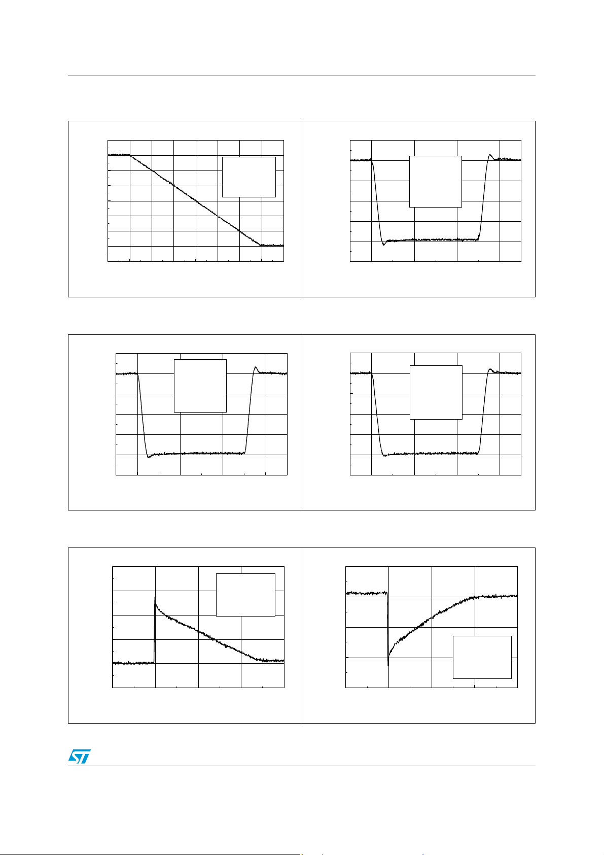
Figure 36. Output voltage response to current
transient - buffers A & B
2.0
1.5
1.0
Vout (V)
0.5
0.0
-0.5
-1 0 1 2 3
Time (µs)
Buffers A & B
VCC=10V
T
=+25°C
AMB
ΔI=0mA to 30mA
-0.10
-0.15
0123
Time (µs)
Figure 37. Output voltage response to current
transient - buffers A & B
0.5
0.0
-0.5
Vout (V)
-1.0
-1.5
-10123
Time (µs)
Buffers A & B
VCC=10V
T
=+25°C
AMB
ΔI=30mA to 0mA
Doc ID 11528 Rev 6 11/17

Electrical characteristics TSL1014
Figure 38. Output voltage response to current
transient - buffers C to N
2.0
1.5
1.0
Vout (V)
0.5
Buffers C to N
VCC=10V
T
=+25°C
AMB
ΔI=0mA to 30mA
0.0
-0.5
-10123
Time (µs)
Figure 40. Output voltage response to current
transient - buffer COM
5
4
3
Buffer COM
VCC=10V
T
=+25°C
AMB
ΔI=0mA to 100mA
Figure 39. Output voltage response to current
transient - buffers C to N
0.5
0.0
-0.5
Vout (V)
Buffers C to N
-1.0
-1.5
-1 0 1 2 3
VCC=10V
T
=+25°C
AMB
ΔI=30mA to 0mA
Time (µs)
Figure 41. Output voltage response to current
transient - buffer COM
1
0
-1
2
Vout (V)
1
0
-1
02468
Time (µs)
Figure 42. Output voltage response to current
transient - buffer COM
1
0
-1
-2
-3
Vout (V)
-4
-5
-6
-5 0 5 10 15 20 25
Time (µs)
Buffer COM
VCC=10V
T
=+25°C
AMB
ΔI=100mA to -100mA
-2
Vout (V)
-3
-4
-5
02468
Buffer COM
VCC=10V
T
=+25°C
AMB
ΔI=100mA to 0m A
Time (µs)
Figure 43. Output voltage response to current
transient - buffer COM
6
5
4
3
2
Vout (V)
1
0
-1
-5 0 5 10 15 20 25 30
Buffer COM
VCC=10V
T
=+25°C
AMB
ΔI=-100mA to +100mA
Time (µs)
12/17 Doc ID 11528 Rev 6

TSL1014 Package information
4 Package information
In order to meet environmental requirements, ST offers these devices in different grades of
ECOPACK
specifications, grade definitions and product status are available at: www.st.com.
ECOPACK
®
packages, depending on their level of environmental compliance. ECOPACK®
®
is an ST trademark.
Doc ID 11528 Rev 6 13/17

Package information TSL1014
Table 5. TQFP48 package mechanical data
Dimensions
Ref.
Millimeters Inches
Min. Typ. Max. Min. Typ. Max.
A 1.6 0.063
A1 0.05 0.15 0.002 0.006
A2 1.35 1.40 1.45 0.053 0.055 0.057
B 0.17 0.22 0.27 0.007 0.009 0.011
C 0.09 0.20 0.0035 0.0079
D 9.00 0.354
D1 7.00 0.276
D3 5.50 0.216
e 0.50 0.020
E 9.00 0.354
E1 7.00 0.276
E3 5.50 0.216
L 0.45 0.60 0.75 0.018 0.024 0.030
L1 1.00 0.039
K 0°3.5°7° 0°3.5°7°
14/17 Doc ID 11528 Rev 6
0110596/C
TSL1014 Ordering information
5 Ordering information
Table 6. Order codes
Order code Temperature range Package Packing Marking
TSL1014IF
Tr ay
SL1014I
TSL1014IFT Tape & reel
TSL1014IYF
TSL1014IYFT
1. Qualification and characterization according to AEC Q100 and Q003 or equivalent, advanced screening
according to AEC Q001 and Q 002 or equivalent.
(1)
(1)
-40° C to +85° C TQFP48
Tr ay
SL1014Y
Tape & reel
Doc ID 11528 Rev 6 15/17
Revision history TSL1014
6 Revision history
Table 7. Document revision history
Date Revision Changes
01-Jul-2005 1 Initial release - Product in full production.
Lead temperature corrected in Table 1 on page 2.
01-Sep-2005 2
07-Mar-2007 3
09-Jun-2008 4
Electrical characteristics graphs re-ordered from Figure 2 on page 6
to Figure 43 on page 12.
Notes added on ESD in Table 1 on page 2.
Maximum operating supply voltage increased in Table 2 on page 2.
Input voltage parameters added in Table 2 on page 2.
limits changed for Buffers C to L in Table 4 on page 5.
V
OL
Electrical characteristics table added for automotive parts.
Order codes added for automotive parts.
typical and maximum values for standard parts in
CC
19-Aug-2008 5
Modified l
Ta bl e 3 .
Updated all curves (Figure 2 to Figure 43).
Added ESD charged device model value in Figure 1.
11-May-2009 6 Modified footnote under Table 6: Order codes.
16/17 Doc ID 11528 Rev 6

TSL1014
Please Read Carefully:
Information in this document is provided solely in connection with ST products. STMicroelectronics NV and its subsidiaries (“ST”) reserve the
right to make changes, corrections, modifications or improvements, to this document, and the products and services described herein at any
time, without notice.
All ST products are sold pursuant to ST’s terms and conditions of sale.
Purchasers are solely responsible for the choice, selection and use of the ST products and services described herein, and ST assumes no
liability whatsoever relating to the choice, selection or use of the ST products and services described herein.
No license, express or implied, by estoppel or otherwise, to any intellectual property rights is granted under this document. If any part of this
document refers to any third party products or services it shall not be deemed a license grant by ST for the use of such third party products
or services, or any intellectual property contained therein or considered as a warranty covering the use in any manner whatsoever of such
third party products or services or any intellectual property contained therein.
UNLESS OTHERWISE SET FORTH IN ST’S TERMS AND CONDITIONS OF SALE ST DISCLAIMS ANY EXPRESS OR IMPLIED
WARRANTY WITH RESPECT TO THE USE AND/OR SALE OF ST PRODUCTS INCLUDING WITHOUT LIMITATION IMPLIED
WARRANTIES OF MERCHANTABILITY, FITNESS FOR A PARTICULAR PURPOSE (AND THEIR EQUIVALENTS UNDER THE LAWS
OF ANY JURISDICTION), OR INFRINGEMENT OF ANY PATENT, COPYRIGHT OR OTHER INTELLECTUAL PROPERTY RIGHT.
UNLESS EXPRESSLY APPROVED IN WRITING BY AN AUTHORIZED ST REPRESENTATIVE, ST PRODUCTS ARE NOT
RECOMMENDED, AUTHORIZED OR WARRANTED FOR USE IN MILITARY, AIR CRAFT, SPACE, LIFE SAVING, OR LIFE SUSTAINING
APPLICATIONS, NOR IN PRODUCTS OR SYSTEMS WHERE FAILURE OR MALFUNCTION MAY RESULT IN PERSONAL INJURY,
DEATH, OR SEVERE PROPERTY OR ENVIRONMENTAL DAMAGE. ST PRODUCTS WHICH ARE NOT SPECIFIED AS "AUTOMOTIVE
GRADE" MAY ONLY BE USED IN AUTOMOTIVE APPLICATIONS AT USER’S OWN RISK.
Resale of ST products with provisions different from the statements and/or technical features set forth in this document shall immediately void
any warranty granted by ST for the ST product or service described herein and shall not create or extend in any manner whatsoever, any
liability of ST.
ST and the ST logo are trademarks or registered trademarks of ST in various countries.
Information in this document supersedes and replaces all information previously supplied.
The ST logo is a registered trademark of STMicroelectronics. All other names are the property of their respective owners.
© 2009 STMicroelectronics - All rights reserved
STMicroelectronics group of companies
Australia - Belgium - Brazil - Canada - China - Czech Republic - Finland - France - Germany - Hong Kong - India - Israel - Italy - Japan -
Malaysia - Malta - Morocco - Philippines - Singapore - Spain - Sweden - Switzerland - United Kingdom - United States of America
www.st.com
Doc ID 11528 Rev 6 17/17
 Loading...