

TSH80, TSH81, TSH82, TSH84
6
.#
34!.$"
9
.ONINVERTING PUT
)NVERTING INPUT
/UTPUT
?
6##
##
.#
INPUT
T
?
6##
6
##
.#
.#
/UTP
UT
?
.#
)NVINPUT
?
6##
6##
.ONINVINPUT
)NVERTINGINPUT
/UTPUT
?
/UTPUT
.ONINVINPUT
)NVERTING INPUT
?
N
?
?
Wide band rail-to-rail operational amplifier with standby function
Datasheet − production data
Features
■ Operating range from 4.5 to 12 V
■ 3 dB-bandwidth: 100 MHz
■ Slew rate 100 V/μs
■ Output current up to 55 mA
■ Input single supply voltage
■ Output rail-to-rail
■ Specified for 150 Ω loads
■ Low distortion, THD 0.1%
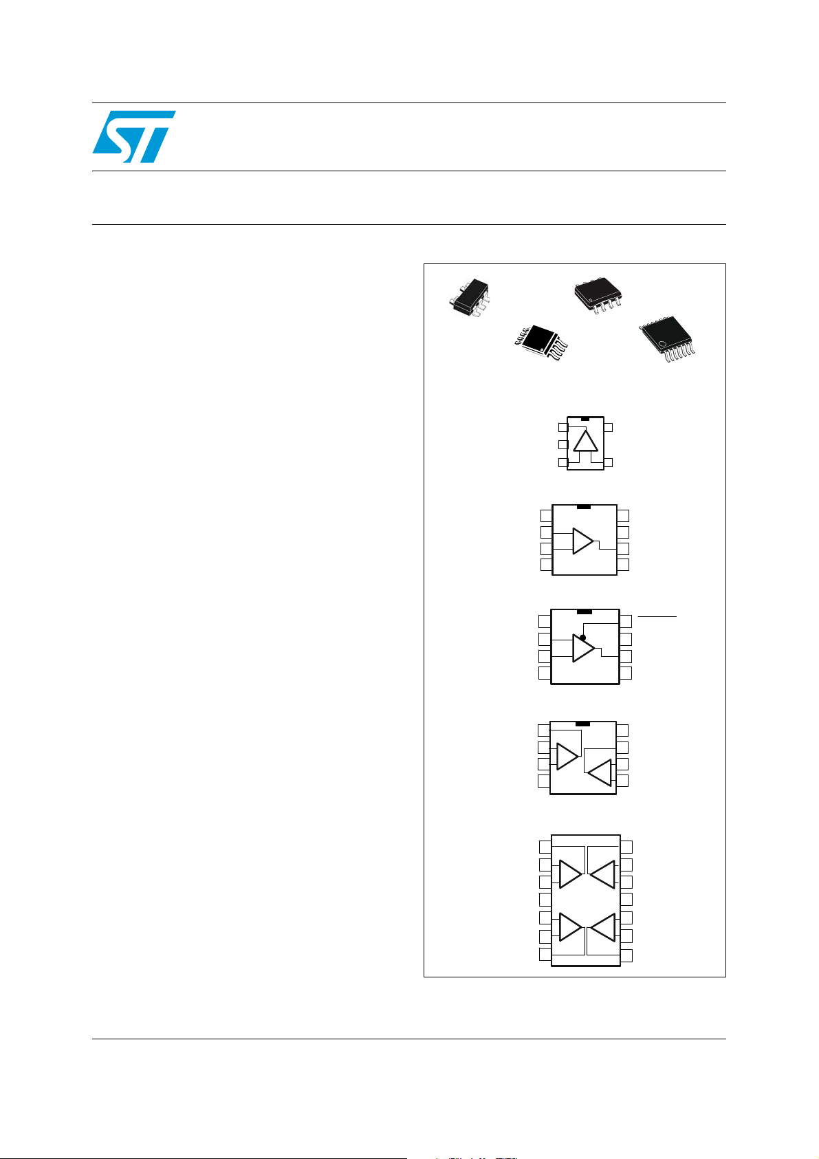
■ SOT23-5, SO, and TSSOP packages
Applications
SOT23-5
TSSOP8
Pin connections TSH80/SOT23-5
/UTPUT
6
##
.ONINVINPU
Pin connections TSH80/SO-8
SO-8
T
6
##
)NVINPUT
TSSOP14
■ Video buffers
■ A/D converter drivers
■ Hi-fi applications
Description
The TSH8x series offers single, dual and quad
operational amplifiers featuring high video
performance with large bandwidth, low distortion
and excellent supply voltage rejection. These
amplifiers also feature large output voltage swings
and a high output current capability to drive
standard 150 Ω loads.
Running at single or dual supply voltages ranging
from 4.5 to 12 V, these amplifiers are tested at 5 V
(±2.5 V) and 10 V (±5 V) supplies.
The TSH81 device also features a standby mode,
which provides the operational amplifier with
a low power consumption and high output
impedance. This function allows power saving or
signal switching/multiplexing for high-speed and
video applications.
For board space and weight saving, the TSH8x
series is proposed in SOT23-5, SO-8, TSSOP8,
and TSSOP14 plastic micropackages.
Pin connections TSH81 SO-8/TSSOP8
Pin connections TSH82 SO-8/TSSOP8
Pin connections TSH84 TSSOP14
/UTPUT
)NVERTING INPUT
.ONINVERT ING INPUT
6##
.ONINVERTING INPUT
NG
)NVERTING INPUT
/UTPUT
?
?
?
?
?
?
?
?
/UTPUT
)NVERTING INPUT
.ONINVER TING INPUT
6
##
.ONINVERTING INPUT
)NVERTING INPUT
/UTPUT
July 2012 Doc ID 9413 Rev 6 1/29
This is information on a product in full production.
www.st.com
1

Contents TSH80, TSH81, TSH82, TSH84
Contents
1 Absolute maximum ratings and operating conditions . . . . . . . . . . . . . 5
2 Electrical characteristics . . . . . . . . . . . . . . . . . . . . . . . . . . . . . . . . . . . . . 6
3 Test conditions . . . . . . . . . . . . . . . . . . . . . . . . . . . . . . . . . . . . . . . . . . . . 18
3.1 Layout precautions . . . . . . . . . . . . . . . . . . . . . . . . . . . . . . . . . . . . . . . . . . 18
3.2 Video capabilities . . . . . . . . . . . . . . . . . . . . . . . . . . . . . . . . . . . . . . . . . . . 19
4 Precautions on asymmetrical supply operation . . . . . . . . . . . . . . . . . 21
5 Package information . . . . . . . . . . . . . . . . . . . . . . . . . . . . . . . . . . . . . . . . 22
5.1 SOT23-5 package information . . . . . . . . . . . . . . . . . . . . . . . . . . . . . . . . . 23
5.2 SO-8 package information . . . . . . . . . . . . . . . . . . . . . . . . . . . . . . . . . . . . 24
5.3 TSSOP8 package information . . . . . . . . . . . . . . . . . . . . . . . . . . . . . . . . . 25
5.4 TSSOP14 package information . . . . . . . . . . . . . . . . . . . . . . . . . . . . . . . . 26
6 Ordering information . . . . . . . . . . . . . . . . . . . . . . . . . . . . . . . . . . . . . . . 27
7 Revision history . . . . . . . . . . . . . . . . . . . . . . . . . . . . . . . . . . . . . . . . . . . 28
2/29 Doc ID 9413 Rev 6

TSH80, TSH81, TSH82, TSH84 List of tables
List of tables
Table 1. Absolute maximum ratings . . . . . . . . . . . . . . . . . . . . . . . . . . . . . . . . . . . . . . . . . . . . . . . . . . 5
Table 2. Operating conditions . . . . . . . . . . . . . . . . . . . . . . . . . . . . . . . . . . . . . . . . . . . . . . . . . . . . . . . 5
Table 3. V
Table 4. V
Table 5. Standby mode - V
Table 6. TSH81 standby control pin status. . . . . . . . . . . . . . . . . . . . . . . . . . . . . . . . . . . . . . . . . . . . 11
Table 7. Video results . . . . . . . . . . . . . . . . . . . . . . . . . . . . . . . . . . . . . . . . . . . . . . . . . . . . . . . . . . . . 20
Table 8. SOT23-5 package mechanical data . . . . . . . . . . . . . . . . . . . . . . . . . . . . . . . . . . . . . . . . . . 23
Table 9. SO-8 package mechanical data . . . . . . . . . . . . . . . . . . . . . . . . . . . . . . . . . . . . . . . . . . . . . 24
Table 10. TSSOP8 package mechanical data . . . . . . . . . . . . . . . . . . . . . . . . . . . . . . . . . . . . . . . . . . 25
Table 11. TSSOP14 package mechanical data . . . . . . . . . . . . . . . . . . . . . . . . . . . . . . . . . . . . . . . . . 26
Table 12. Order codes . . . . . . . . . . . . . . . . . . . . . . . . . . . . . . . . . . . . . . . . . . . . . . . . . . . . . . . . . . . . 27
Table 13. Document revision history . . . . . . . . . . . . . . . . . . . . . . . . . . . . . . . . . . . . . . . . . . . . . . . . . 28
+ = +5 V, VCC- = GND, Vic = 2.5 V, T
CC
= 25 °C
amb
(unless otherwise specified) . . . . . . . . . . . . . . . . . . . . . . . . . . . . . . . . . . . . . . . . . . . . . . . . . 6
+ = +5 V, VCC- = -5 V, Vic = GND, T
CC
= 25 °C
amb
(unless otherwise specified) . . . . . . . . . . . . . . . . . . . . . . . . . . . . . . . . . . . . . . . . . . . . . . . . . 9
+, VCC-, T
CC
= 25 °C (unless otherwise specified). . . . . . . . . . . . . . 11
amb
Doc ID 9413 Rev 6 3/29

List of figures TSH80, TSH81, TSH82, TSH84
List of figures
Figure 1. Closed loop gain and phase vs. frequency (gain = +2, VCC = ±2.5 V) . . . . . . . . . . . . . . . . 12
Figure 2. Overshoot vs. output capacitance (V
Figure 3. Closed loop gain and phase vs. frequency (gain = -10, V
Figure 4. Closed loop gain and phase vs. frequency (gain = +11, V
Figure 5. Large signal measurement – positive slew rate (V
Figure 6. Large signal measurement – negative slew rate (V
Figure 7. Small signal measurement – rise time (V
Figure 8. Small signal measurement – fall time (V
Figure 9. Channel separation (crosstalk) vs. frequency schematic (V
Figure 10. Channel separation (crosstalk) vs. frequency (V
Figure 11. Equivalent input noise voltage (V
Figure 12. Maximum output swing (V
Figure 13. Standby mode - T
on
, T
Figure 14. Third order intermodulation (V
Figure 15. Group delay (V
= ±2.5 V) . . . . . . . . . . . . . . . . . . . . . . . . . . . . . . . . . . . . . . . . . . . . . . . . 14
CC
= ±2.5 V). . . . . . . . . . . . . . . . . . . . . . . . . . . . . . . . . . . . . . . . 13
CC
off (VCC
= ±2.5 V) . . . . . . . . . . . . . . . . . . . . . . . . . . . . . . . . . . . . . . 14
CC
Figure 16. Closed loop gain and phase vs. frequency (gain = +2, V
Figure 17. Overshoot vs. output capacitance (V
Figure 18. Closed loop gain and phase vs. frequency (gain = -10, V
Figure 19. Closed loop gain and phase vs. frequency (gain = +11, V
Figure 20. Large signal measurement - positive slew rate (V
Figure 21. Large signal measurement - negative slew rate (V
Figure 22. Small signal measurement – rise time (V
Figure 23. Small signal measurement – fall time (V
Figure 24. Channel separation (crosstalk) vs. frequency schematic (V
Figure 25. Channel separation (crosstalk) vs. frequency (V
Figure 26. Equivalent input noise voltage (V
Figure 27. Maximum output swing (V
Figure 28. Standby mode - T
on
, T
Figure 29. Third order intermodulation (V
Figure 30. Group delay V
= ±5 V. . . . . . . . . . . . . . . . . . . . . . . . . . . . . . . . . . . . . . . . . . . . . . . . . . . 17
CC
= ±5 V) . . . . . . . . . . . . . . . . . . . . . . . . . . . . . . . . . . . . . . . . . 16
CC
off (VCC
= ±5 V) . . . . . . . . . . . . . . . . . . . . . . . . . . . . . . . . . . . . . . . . 17
CC
Figure 31. CCIR330 video line. . . . . . . . . . . . . . . . . . . . . . . . . . . . . . . . . . . . . . . . . . . . . . . . . . . . . . . 18
Figure 32. Measurement on Rohde and Schwarz VSA . . . . . . . . . . . . . . . . . . . . . . . . . . . . . . . . . . . . 19
Figure 33. Asymmetrical supply schematic diagram . . . . . . . . . . . . . . . . . . . . . . . . . . . . . . . . . . . . . . 21
Figure 34. Use of the TSH8x in a gain = -1 configuration . . . . . . . . . . . . . . . . . . . . . . . . . . . . . . . . . . 21
Figure 35. SOT23-5 package outline . . . . . . . . . . . . . . . . . . . . . . . . . . . . . . . . . . . . . . . . . . . . . . . . . . 23
Figure 36. SO-8 package outline . . . . . . . . . . . . . . . . . . . . . . . . . . . . . . . . . . . . . . . . . . . . . . . . . . . . . 24
Figure 37. TSSOP8 package outline . . . . . . . . . . . . . . . . . . . . . . . . . . . . . . . . . . . . . . . . . . . . . . . . . . 25
Figure 38. TSSOP14 package outline . . . . . . . . . . . . . . . . . . . . . . . . . . . . . . . . . . . . . . . . . . . . . . . . . 26
= ±2.5 V) . . . . . . . . . . . . . . . . . . . . . . . . . . . . . . . 12
CC
= ±2.5 V) . . . . . . . . . . . . . . . . . . . . . 12
CC
CC
= ±2.5 V) . . . . . . . . . . . . . . . . . . . . . . . . . . . . 13
CC
= ±2.5 V). . . . . . . . . . . . . . . . . . . . . . . . . . . . . 13
CC
= ±2.5 V) . . . . . . . . . . . . . . . . . . . . . . 13
= ±2.5 V) . . . . . . . . . . . . . . . . . . . . . . . . . . . . . . . . . . 13
CC
CC
= ±2.5 V) . . . . . . . . . . . . . . . 12
CC
= ±2.5 V) . . . . . . . . . . . . . . . 12
CC
= ±2.5 V) . . . . . . . . . . . . . . . . . . . . 12
= ±2.5 V). . . . . . . . . . . . . . 13
CC
= ±2.5 V) . . . . . . . . . . . . . . . . . . . . . . . . . . . . . . . . . . . . 14
= ±5 V) . . . . . . . . . . . . . . . . . 15
= ±5 V). . . . . . . . . . . . . . . . . . . . . . . . . . . . . . . . . 15
CC
= ±5 V) . . . . . . . . . . . . . . . . . . . . . . . . . . . . . 16
CC
= ±5 V) . . . . . . . . . . . . . . . . . . . . . . . . . . . . . . 16
CC
= ±5 V). . . . . . . . . . . . . . . . . . . . . . . . . . . . . . . . . . . . 16
CC
CC
CC
= ±5 V) . . . . . . . . . . . . . . . . . 15
CC
= ±5 V) . . . . . . . . . . . . . . . . 15
CC
= ±5 V) . . . . . . . . . . . . . . . . . . . . . . . 15
CC
= ±5 V) . . . . . . . . . . . . . . . . . . . . . . 15
CC
= ±5 V) . . . . . . . . . . . . . . . 16
CC
= ±5 V) . . . . . . . . . . . . . . . . . . . . . . . . 16
= ±5 V). . . . . . . . . . . . . . . . . . . . . . . . . . . . . . . . . . . . . . 17
4/29 Doc ID 9413 Rev 6
TSH80, TSH81, TSH82, TSH84 Absolute maximum ratings and operating conditions
1 Absolute maximum ratings and operating conditions
Table 1. Absolute maximum ratings
Symbol Parameter Value Unit
(3)
(1)
(6)
(2)
(5)
(7)
(4)
14 V
±2 V
±6 V
80
28
°C/W
37
32
250
157
°C/W
130
110
2
0.2
1
kV
T
V
V
T
CC
id
V
oper
stg
T
i
j
Supply voltage
Differential input voltage
Input voltage
Operating free air temperature range -40 to +85 °C
Storage temperature -65 to +150 °C
Maximum junction temperature 150 °C
Thermal resistance junction to case
SOT23-5
R
thjc
SO8
TSSOP8
TSSOP14
Thermal resistance junction to ambient area
SOT23-5
R
thja
SO8
TSSOP8
TSSOP14
HBM: human body model
ESD
MM: machine model
CDM: charged device model
1. All voltage values, except differential voltage are with respect to network ground terminal.
2. Differential voltages are the non inverting input terminal with respect to the inverting terminal.
3. The magnitude of input and output must never exceed VCC +0.3 V.
4. Short-circuits can cause excessive heating.
5. Human body model: a 100 pF capacitor is charged to the specified voltage, then discharged through
a 1.5 kΩ resistor between two pins of the device. This is done for all couples of connected pin combinations
while the other pins are floating.
6. Machine model: a 200 pF capacitor is charged to the specified voltage, then discharged directly between
two pins of the device with no external series resistor (internal resistor < 5 Ω). This is done for all couples of
connected pin combinations while the other pins are floating.
7. Charged device model: all pins and package are charged together to the specified voltage and then
discharged directly to the ground through only one pin. This is done for all pins.
Table 2. Operating conditions
Symbol Parameter Value Unit
V
CC
V
IC
Standby (pin 8) Threshold on pin 8 for TSH81 (V
Supply voltage 4.5 to 12 V
Common mode input voltage range V
CC
-
to (V
CC
-
) to (V
+
-1.1) V
CC
+
)V
CC
Doc ID 9413 Rev 6 5/29
Electrical characteristics TSH80, TSH81, TSH82, TSH84
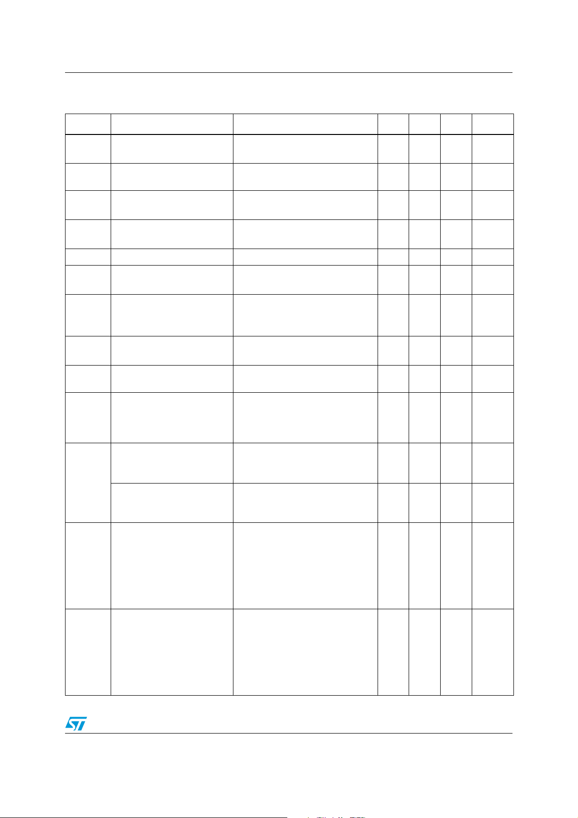
2 Electrical characteristics
Table 3. V
+
= +5 V, V
CC
(unless otherwise specified)
Symbol Parameter Test conditions Min. Typ. Max. Unit
-
= GND, Vic = 2.5 V, T
CC
amb
= 25 °C
| Input offset voltage
|V
io
ΔV
C
I
CMR
SVR
PSR
A
Input offset voltage drift vs.
io
temperature
Input offset current
I
io
Input bias current
I
ib
Input capacitance 0.3 pF
in
Supply current per operator
CC
Common mode rejection ratio
/δVio)
(δV
ic
Supply voltage rejection ratio
(δV
/δVio)
CC
Power supply rejection ratio
(δV
/δV
CC
Large signal voltage gain
vd
|Source|
I
o
Sink
out
= 25 °C
T
amb
< T
T
min
T
min
T
amb
T
min
T
amb
T
min
T
amb
T
min
+0.1< V
T
amb
T
min
T
amb
T
min
)
Positive and negative rail 75 dB
= 150 Ω connected to 1.5 V and
R
L
V
out
T
amb
T
min
V
=+1, V
id
T
amb
T
min
V
=-1, V
id
T
amb
T
min
< T
amb
< T
< T
amb
= 25 °C
< T
< T
amb
= 25 °C
< T
< T
amb
= 25 °C
< T
< T
amb
< 3.9 V and V
ic
= 25 °C
< T
amb
= 25 °C
< T
< T
amb
= 1 V to 4 V
= 25 °C
< T
amb
connected to 1.5 V
out
= 25 °C
< T
amb
connected to 1.5 V
out
= 25 °C
< T
amb
max
max
max
max
max
< T
max
< T
< T
< T
max
max
max
max
out
=2.5V
72
70
68
65
75
70
35
28
33
28
1.1 10
12
mV
3 μV/°C
0.1 3.5
5
615
20
8.2 10.5
11.5
μA
μA
mA
97 dB
75
84
dB
dB
55 mA
55
6/29 Doc ID 9413 Rev 6
TSH80, TSH81, TSH82, TSH84 Electrical characteristics
Table 3. V
+
= +5 V, V
CC
-
= GND, Vic = 2.5 V, T
CC
amb
= 25 °C
(unless otherwise specified) (continued)
Symbol Parameter Test conditions Min. Typ. Max. Unit
= 25 °C
T
amb
4.36
4.2
4.60
4.5
4.1
4.4
4.85
(1)
4.90
4.93
4.66
4.90
4.92
4.93
48
150
54
55
56
220
400
105
76
61
200
450
65
55
87 MHz
104
105
V
V
High level output voltage
oh
Low level output voltage
ol
GBP Gain bandwidth product
Bw Bandwidth at -3 dB
SR Slew rate
φm Phase margin R
en
Equivalent input noise
voltage
= 150 Ω connected to GND
R
L
R
= 600 Ω connected to GND
L
R
= 2 kΩ connected to GND
L
R
= 10 kΩ connected to GND
L
= 150 Ω connected to 2.5 V
R
L
R
= 600 Ω connected to 2.5 V
L
R
= 2 kΩ connected to 2.5 V
L
R
= 10 kΩ connected to 2.5 V
L
< T
T
min
amb
< T
max
RL = 150 Ω connected to GND
R
= 150 Ω connected to 2.5 V
L
T
= 25 °C
amb
= 150 Ω connected to GND
R
L
R
= 600 Ω connected to GND
L
R
= 2 kΩ connected to GND
L
R
= 10 kΩ connected to GND
L
= 150 Ω connected to 2.5 V
R
L
R
= 600 Ω connected to 2.5 V
L
R
= 2 kΩ connected to 2.5 V
L
R
= 10 kΩ connected to 2.5 V
L
< T
T
min
amb
< T
max
RL = 150 Ω connected to GND
R
= 150 Ω connected to 2.5 V
L
F=10MHz
A
= +11
VCL
A
= -10
VCL
= +1
A
VCL
R
= 150 Ω connected to 2.5 V
L
= +2
A
VCL
R
= 150 Ω // CL to 2.5 V
L
= 5 pF
C
L
C
= 30 pF 60
L
= 150 Ω // 30 pF to 2.5 V 40 ° (degree)
L
F = 100 kHz 11 nV/
V
mV
MHz
V/μs
√
Hz
THD Total harmonic distortion
IM2
Second order intermodulation
product
A
= +2, F = 4 MHz
VCL
R
= 150 Ω // 30 pF to 2.5 V
L
= 1V
V
A
V
VCL
out
out
= 2V
= +2, V
pp
pp
out
=2V
pp
RL= 150 Ω connected to 2.5 V
F
= 180 kHz, F
in1
=280kHz
in2
-61
-54
-76 dBc
spurious measurement at 100 kHz
Doc ID 9413 Rev 6 7/29
dB
Electrical characteristics TSH80, TSH81, TSH82, TSH84
Table 3. V
+
= +5 V, V
CC
-
= GND, Vic = 2.5 V, T
CC
amb
= 25 °C
(unless otherwise specified) (continued)
Symbol Parameter Test conditions Min. Typ. Max. Unit
A
= +2, V
VCL
IM3
Third order intermodulation
product
RL= 150 Ω to 2.5 V
F
= 180 kHz, F
in1
spurious measurement at 400 kHz
A
=+2, RL= 150 Ω to 2.5 V
ΔG Differential gain
Df Differential phase
VCL
F=4.5MHz, V
=+2, RL= 150 Ω to 2.5 V
A
VCL
F=4.5MHz, V
Gf Gain flatness F = DC to 6 MHz, A
Vo1/Vo2 Channel separation F = 1 MHz to 10 MHz 65 dB
1. Tested on the TSH80ILT device only.
out
=2V
in2
=2V
out
=2V
out
pp
=280kHz
pp
pp
=+2 0.2 dB
VCL
-68 dBc
0.5 %
0.5 ° (degree)
8/29 Doc ID 9413 Rev 6
TSH80, TSH81, TSH82, TSH84 Electrical characteristics
Table 4. V
+
= +5 V, V
CC
-
= -5 V, Vic = GND, T
CC
amb
= 25 °C
(unless otherwise specified)
Symbol Parameter Test conditions Min. Typ. Max. Unit
| Input offset voltage
|V
io
ΔV
I
I
C
I
CC
CMR
SVR
PSR
A
Input offset voltage drift vs.
io
temperature
Input offset current
io
Input bias current
ib
Input capacitance 0.7 pF
in
Supply current per operator
Common mode rejection ratio
/δVio)
(δV
ic
Supply voltage rejection ratio
(δV
/δVio)
CC
Power supply rejection ratio
(δV
/δV
CC
out
Large signal voltage gain
vd
|Source|
I
o
Sink
V
High level output voltage
oh
= 25 °C
T
amb
< T
T
min
T
min
T
amb
T
min
T
amb
T
min
T
amb
T
min
-4.9 < V
T
amb
T
min
T
amb
T
min
)
Positive and negative rail 75 dB
R
= 150 Ω connected to GND
L
V
out
T
amb
T
min
V
=+1, V
id
T
amb
T
min
=-1, V
V
id
T
amb
T
min
T
amb
R
L
R
L
R
L
R
L
T
min
RL = 150 Ω connected to GND
< T
amb
max
< T
< T
amb
max
= 25 °C
< T
< T
amb
max
= 25 °C
< T
< T
amb
max
= 25 °C
< T
< T
amb
max
< 3.9 V and V
ic
out
=GND
= 25 °C
< T
amb
< T
max
= 25 °C
< T
< T
amb
max
= -4 to +4
= 25 °C
< T
< T
amb
max
connected to 1.5 V
out
= 25 °C
< T
< T
amb
max
connected to 1.5 V
out
= 25 °C
< T
amb
< T
max
= 25 °C
= 150 Ω connected to GND
= 600 Ω connected to GND
= 2 kΩ connected to GND
= 10 kΩ connected to GND
< T
< T
amb
max
8172106 dB
71
65
75
70
35
28
30
28
4.2
4.1
0.8 10
12
2 μV/°C
0.1 3.5
5
615
20
9.8 12.3
13.4
77
86
55
55
4.36
4.85
4.9
4.93
mV
μA
μA
mA
dB
dB
mA
V
T
= 25 °C
amb
= 150 Ω connected to GND
R
L
R
= 600 Ω connected to GND
L
R
V
Low level output voltage
ol
= 2 kΩ connected to GND
L
R
= 10 kΩ connected to GND
L
< T
T
min
amb
< T
max
-4.63
-4.86
-4.9
-4.93
RL = 150 Ω connected to GND
-4.4
mV
-4.3
Doc ID 9413 Rev 6 9/29
 Loading...