

TSH80, TSH81, TSH82, TSH84
6
.#
34!.$"
9
.ONINVERTING PUT
)NVERTING INPUT
/UTPUT
?
6##
##
.#
INPUT
T
?
6##
6
##
.#
.#
/UTP
UT
?
.#
)NVINPUT
?
6##
6##
.ONINVINPUT
)NVERTINGINPUT
/UTPUT
?
/UTPUT
.ONINVINPUT
)NVERTING INPUT
?
N
?
?
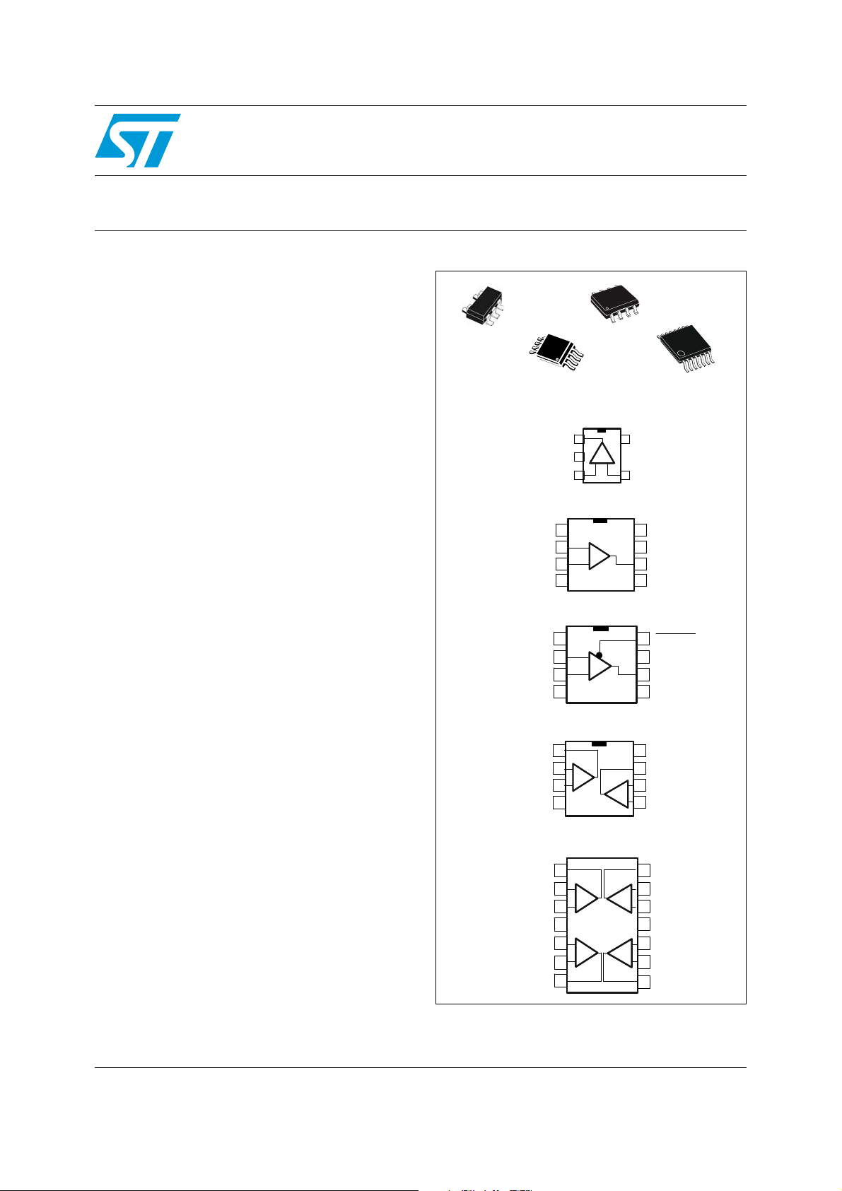
Wide band rail-to-rail operational amplifier with standby function
Datasheet − production data
Features
■ Operating range from 4.5 to 12 V
■ 3 dB-bandwidth: 100 MHz
■ Slew rate 100 V/μs
■ Output current up to 55 mA
■ Input single supply voltage
■ Output rail-to-rail
■ Specified for 150 Ω loads
■ Low distortion, THD 0.1%
■ SOT23-5, SO, and TSSOP packages
Applications
SOT23-5
TSSOP8
Pin connections TSH80/SOT23-5
/UTPUT
6
##
.ONINVINPU
Pin connections TSH80/SO-8
SO-8
T
6
##
)NVINPUT
TSSOP14
■ Video buffers
■ A/D converter drivers
■ Hi-fi applications
Description
The TSH8x series offers single, dual and quad
operational amplifiers featuring high video
performance with large bandwidth, low distortion
and excellent supply voltage rejection. These
amplifiers also feature large output voltage swings
and a high output current capability to drive
standard 150 Ω loads.
Running at single or dual supply voltages ranging
from 4.5 to 12 V, these amplifiers are tested at 5 V
(±2.5 V) and 10 V (±5 V) supplies.
The TSH81 device also features a standby mode,
which provides the operational amplifier with
a low power consumption and high output
impedance. This function allows power saving or
signal switching/multiplexing for high-speed and
video applications.
For board space and weight saving, the TSH8x
series is proposed in SOT23-5, SO-8, TSSOP8,
and TSSOP14 plastic micropackages.
Pin connections TSH81 SO-8/TSSOP8
Pin connections TSH82 SO-8/TSSOP8
Pin connections TSH84 TSSOP14
/UTPUT
)NVERTING INPUT
.ONINVERT ING INPUT
6##
.ONINVERTING INPUT
NG
)NVERTING INPUT
/UTPUT
?
?
?
?
?
?
?
?
/UTPUT
)NVERTING INPUT
.ONINVER TING INPUT
6
##
.ONINVERTING INPUT
)NVERTING INPUT
/UTPUT
July 2012 Doc ID 9413 Rev 6 1/29
This is information on a product in full production.
www.st.com
1

Contents TSH80, TSH81, TSH82, TSH84
Contents
1 Absolute maximum ratings and operating conditions . . . . . . . . . . . . . 5
2 Electrical characteristics . . . . . . . . . . . . . . . . . . . . . . . . . . . . . . . . . . . . . 6
3 Test conditions . . . . . . . . . . . . . . . . . . . . . . . . . . . . . . . . . . . . . . . . . . . . 18
3.1 Layout precautions . . . . . . . . . . . . . . . . . . . . . . . . . . . . . . . . . . . . . . . . . . 18
3.2 Video capabilities . . . . . . . . . . . . . . . . . . . . . . . . . . . . . . . . . . . . . . . . . . . 19
4 Precautions on asymmetrical supply operation . . . . . . . . . . . . . . . . . 21
5 Package information . . . . . . . . . . . . . . . . . . . . . . . . . . . . . . . . . . . . . . . . 22
5.1 SOT23-5 package information . . . . . . . . . . . . . . . . . . . . . . . . . . . . . . . . . 23
5.2 SO-8 package information . . . . . . . . . . . . . . . . . . . . . . . . . . . . . . . . . . . . 24
5.3 TSSOP8 package information . . . . . . . . . . . . . . . . . . . . . . . . . . . . . . . . . 25
5.4 TSSOP14 package information . . . . . . . . . . . . . . . . . . . . . . . . . . . . . . . . 26
6 Ordering information . . . . . . . . . . . . . . . . . . . . . . . . . . . . . . . . . . . . . . . 27
7 Revision history . . . . . . . . . . . . . . . . . . . . . . . . . . . . . . . . . . . . . . . . . . . 28
2/29 Doc ID 9413 Rev 6

TSH80, TSH81, TSH82, TSH84 List of tables
List of tables
Table 1. Absolute maximum ratings . . . . . . . . . . . . . . . . . . . . . . . . . . . . . . . . . . . . . . . . . . . . . . . . . . 5
Table 2. Operating conditions . . . . . . . . . . . . . . . . . . . . . . . . . . . . . . . . . . . . . . . . . . . . . . . . . . . . . . . 5
Table 3. V
Table 4. V
Table 5. Standby mode - V
Table 6. TSH81 standby control pin status. . . . . . . . . . . . . . . . . . . . . . . . . . . . . . . . . . . . . . . . . . . . 11
Table 7. Video results . . . . . . . . . . . . . . . . . . . . . . . . . . . . . . . . . . . . . . . . . . . . . . . . . . . . . . . . . . . . 20
Table 8. SOT23-5 package mechanical data . . . . . . . . . . . . . . . . . . . . . . . . . . . . . . . . . . . . . . . . . . 23
Table 9. SO-8 package mechanical data . . . . . . . . . . . . . . . . . . . . . . . . . . . . . . . . . . . . . . . . . . . . . 24
Table 10. TSSOP8 package mechanical data . . . . . . . . . . . . . . . . . . . . . . . . . . . . . . . . . . . . . . . . . . 25
Table 11. TSSOP14 package mechanical data . . . . . . . . . . . . . . . . . . . . . . . . . . . . . . . . . . . . . . . . . 26
Table 12. Order codes . . . . . . . . . . . . . . . . . . . . . . . . . . . . . . . . . . . . . . . . . . . . . . . . . . . . . . . . . . . . 27
Table 13. Document revision history . . . . . . . . . . . . . . . . . . . . . . . . . . . . . . . . . . . . . . . . . . . . . . . . . 28
+ = +5 V, VCC- = GND, Vic = 2.5 V, T
CC
= 25 °C
amb
(unless otherwise specified) . . . . . . . . . . . . . . . . . . . . . . . . . . . . . . . . . . . . . . . . . . . . . . . . . 6
+ = +5 V, VCC- = -5 V, Vic = GND, T
CC
= 25 °C
amb
(unless otherwise specified) . . . . . . . . . . . . . . . . . . . . . . . . . . . . . . . . . . . . . . . . . . . . . . . . . 9
+, VCC-, T
CC
= 25 °C (unless otherwise specified). . . . . . . . . . . . . . 11
amb
Doc ID 9413 Rev 6 3/29

List of figures TSH80, TSH81, TSH82, TSH84
List of figures
Figure 1. Closed loop gain and phase vs. frequency (gain = +2, VCC = ±2.5 V) . . . . . . . . . . . . . . . . 12
Figure 2. Overshoot vs. output capacitance (V
Figure 3. Closed loop gain and phase vs. frequency (gain = -10, V
Figure 4. Closed loop gain and phase vs. frequency (gain = +11, V
Figure 5. Large signal measurement – positive slew rate (V
Figure 6. Large signal measurement – negative slew rate (V
Figure 7. Small signal measurement – rise time (V
Figure 8. Small signal measurement – fall time (V
Figure 9. Channel separation (crosstalk) vs. frequency schematic (V
Figure 10. Channel separation (crosstalk) vs. frequency (V
Figure 11. Equivalent input noise voltage (V
Figure 12. Maximum output swing (V
Figure 13. Standby mode - T
on
, T
Figure 14. Third order intermodulation (V
Figure 15. Group delay (V
= ±2.5 V) . . . . . . . . . . . . . . . . . . . . . . . . . . . . . . . . . . . . . . . . . . . . . . . . 14
CC
= ±2.5 V). . . . . . . . . . . . . . . . . . . . . . . . . . . . . . . . . . . . . . . . 13
CC
off (VCC
= ±2.5 V) . . . . . . . . . . . . . . . . . . . . . . . . . . . . . . . . . . . . . . 14
CC
Figure 16. Closed loop gain and phase vs. frequency (gain = +2, V
Figure 17. Overshoot vs. output capacitance (V
Figure 18. Closed loop gain and phase vs. frequency (gain = -10, V
Figure 19. Closed loop gain and phase vs. frequency (gain = +11, V
Figure 20. Large signal measurement - positive slew rate (V
Figure 21. Large signal measurement - negative slew rate (V
Figure 22. Small signal measurement – rise time (V
Figure 23. Small signal measurement – fall time (V
Figure 24. Channel separation (crosstalk) vs. frequency schematic (V
Figure 25. Channel separation (crosstalk) vs. frequency (V
Figure 26. Equivalent input noise voltage (V
Figure 27. Maximum output swing (V
Figure 28. Standby mode - T
on
, T
Figure 29. Third order intermodulation (V
Figure 30. Group delay V
= ±5 V. . . . . . . . . . . . . . . . . . . . . . . . . . . . . . . . . . . . . . . . . . . . . . . . . . . 17
CC
= ±5 V) . . . . . . . . . . . . . . . . . . . . . . . . . . . . . . . . . . . . . . . . . 16
CC
off (VCC
= ±5 V) . . . . . . . . . . . . . . . . . . . . . . . . . . . . . . . . . . . . . . . . 17
CC
Figure 31. CCIR330 video line. . . . . . . . . . . . . . . . . . . . . . . . . . . . . . . . . . . . . . . . . . . . . . . . . . . . . . . 18
Figure 32. Measurement on Rohde and Schwarz VSA . . . . . . . . . . . . . . . . . . . . . . . . . . . . . . . . . . . . 19
Figure 33. Asymmetrical supply schematic diagram . . . . . . . . . . . . . . . . . . . . . . . . . . . . . . . . . . . . . . 21
Figure 34. Use of the TSH8x in a gain = -1 configuration . . . . . . . . . . . . . . . . . . . . . . . . . . . . . . . . . . 21
Figure 35. SOT23-5 package outline . . . . . . . . . . . . . . . . . . . . . . . . . . . . . . . . . . . . . . . . . . . . . . . . . . 23
Figure 36. SO-8 package outline . . . . . . . . . . . . . . . . . . . . . . . . . . . . . . . . . . . . . . . . . . . . . . . . . . . . . 24
Figure 37. TSSOP8 package outline . . . . . . . . . . . . . . . . . . . . . . . . . . . . . . . . . . . . . . . . . . . . . . . . . . 25
Figure 38. TSSOP14 package outline . . . . . . . . . . . . . . . . . . . . . . . . . . . . . . . . . . . . . . . . . . . . . . . . . 26
= ±2.5 V) . . . . . . . . . . . . . . . . . . . . . . . . . . . . . . . 12
CC
= ±2.5 V) . . . . . . . . . . . . . . . . . . . . . 12
CC
CC
= ±2.5 V) . . . . . . . . . . . . . . . . . . . . . . . . . . . . 13
CC
= ±2.5 V). . . . . . . . . . . . . . . . . . . . . . . . . . . . . 13
CC
= ±2.5 V) . . . . . . . . . . . . . . . . . . . . . . 13
= ±2.5 V) . . . . . . . . . . . . . . . . . . . . . . . . . . . . . . . . . . 13
CC
CC
= ±2.5 V) . . . . . . . . . . . . . . . 12
CC
= ±2.5 V) . . . . . . . . . . . . . . . 12
CC
= ±2.5 V) . . . . . . . . . . . . . . . . . . . . 12
= ±2.5 V). . . . . . . . . . . . . . 13
CC
= ±2.5 V) . . . . . . . . . . . . . . . . . . . . . . . . . . . . . . . . . . . . 14
= ±5 V) . . . . . . . . . . . . . . . . . 15
= ±5 V). . . . . . . . . . . . . . . . . . . . . . . . . . . . . . . . . 15
CC
= ±5 V) . . . . . . . . . . . . . . . . . . . . . . . . . . . . . 16
CC
= ±5 V) . . . . . . . . . . . . . . . . . . . . . . . . . . . . . . 16
CC
= ±5 V). . . . . . . . . . . . . . . . . . . . . . . . . . . . . . . . . . . . 16
CC
CC
CC
= ±5 V) . . . . . . . . . . . . . . . . . 15
CC
= ±5 V) . . . . . . . . . . . . . . . . 15
CC
= ±5 V) . . . . . . . . . . . . . . . . . . . . . . . 15
CC
= ±5 V) . . . . . . . . . . . . . . . . . . . . . . 15
CC
= ±5 V) . . . . . . . . . . . . . . . 16
CC
= ±5 V) . . . . . . . . . . . . . . . . . . . . . . . . 16
= ±5 V). . . . . . . . . . . . . . . . . . . . . . . . . . . . . . . . . . . . . . 17
4/29 Doc ID 9413 Rev 6
TSH80, TSH81, TSH82, TSH84 Absolute maximum ratings and operating conditions
1 Absolute maximum ratings and operating conditions
Table 1. Absolute maximum ratings
Symbol Parameter Value Unit
(3)
(1)
(6)
(2)
(5)
(7)
(4)
14 V
±2 V
±6 V
80
28
°C/W
37
32
250
157
°C/W
130
110
2
0.2
1
kV
T
V
V
T
CC
id
V
oper
stg
T
i
j
Supply voltage
Differential input voltage
Input voltage
Operating free air temperature range -40 to +85 °C
Storage temperature -65 to +150 °C
Maximum junction temperature 150 °C
Thermal resistance junction to case
SOT23-5
R
thjc
SO8
TSSOP8
TSSOP14
Thermal resistance junction to ambient area
SOT23-5
R
thja
SO8
TSSOP8
TSSOP14
HBM: human body model
ESD
MM: machine model
CDM: charged device model
1. All voltage values, except differential voltage are with respect to network ground terminal.
2. Differential voltages are the non inverting input terminal with respect to the inverting terminal.
3. The magnitude of input and output must never exceed VCC +0.3 V.
4. Short-circuits can cause excessive heating.
5. Human body model: a 100 pF capacitor is charged to the specified voltage, then discharged through
a 1.5 kΩ resistor between two pins of the device. This is done for all couples of connected pin combinations
while the other pins are floating.
6. Machine model: a 200 pF capacitor is charged to the specified voltage, then discharged directly between
two pins of the device with no external series resistor (internal resistor < 5 Ω). This is done for all couples of
connected pin combinations while the other pins are floating.
7. Charged device model: all pins and package are charged together to the specified voltage and then
discharged directly to the ground through only one pin. This is done for all pins.
Table 2. Operating conditions
Symbol Parameter Value Unit
V
CC
V
IC
Standby (pin 8) Threshold on pin 8 for TSH81 (V
Supply voltage 4.5 to 12 V
Common mode input voltage range V
CC
-
to (V
CC
-
) to (V
+
-1.1) V
CC
+
)V
CC
Doc ID 9413 Rev 6 5/29
Electrical characteristics TSH80, TSH81, TSH82, TSH84
2 Electrical characteristics
Table 3. V
+
= +5 V, V
CC
(unless otherwise specified)
Symbol Parameter Test conditions Min. Typ. Max. Unit
-
= GND, Vic = 2.5 V, T
CC
amb
= 25 °C
| Input offset voltage
|V
io
ΔV
C
I
CMR
SVR
PSR
A
Input offset voltage drift vs.
io
temperature
Input offset current
I
io
Input bias current
I
ib
Input capacitance 0.3 pF
in
Supply current per operator
CC
Common mode rejection ratio
/δVio)
(δV
ic
Supply voltage rejection ratio
(δV
/δVio)
CC
Power supply rejection ratio
(δV
/δV
CC
Large signal voltage gain
vd
|Source|
I
o
Sink
out
= 25 °C
T
amb
< T
T
min
T
min
T
amb
T
min
T
amb
T
min
T
amb
T
min
+0.1< V
T
amb
T
min
T
amb
T
min
)
Positive and negative rail 75 dB
= 150 Ω connected to 1.5 V and
R
L
V
out
T
amb
T
min
V
=+1, V
id
T
amb
T
min
V
=-1, V
id
T
amb
T
min
< T
amb
< T
< T
amb
= 25 °C
< T
< T
amb
= 25 °C
< T
< T
amb
= 25 °C
< T
< T
amb
< 3.9 V and V
ic
= 25 °C
< T
amb
= 25 °C
< T
< T
amb
= 1 V to 4 V
= 25 °C
< T
amb
connected to 1.5 V
out
= 25 °C
< T
amb
connected to 1.5 V
out
= 25 °C
< T
amb
max
max
max
max
max
< T
max
< T
< T
< T
max
max
max
max
out
=2.5V
72
70
68
65
75
70
35
28
33
28
1.1 10
12
mV
3 μV/°C
0.1 3.5
5
615
20
8.2 10.5
11.5
μA
μA
mA
97 dB
75
84
dB
dB
55 mA
55
6/29 Doc ID 9413 Rev 6
TSH80, TSH81, TSH82, TSH84 Electrical characteristics
Table 3. V
+
= +5 V, V
CC
-
= GND, Vic = 2.5 V, T
CC
amb
= 25 °C
(unless otherwise specified) (continued)
Symbol Parameter Test conditions Min. Typ. Max. Unit
= 25 °C
T
amb
4.36
4.2
4.60
4.5
4.1
4.4
4.85
(1)
4.90
4.93
4.66
4.90
4.92
4.93
48
150
54
55
56
220
400
105
76
61
200
450
65
55
87 MHz
104
105
V
V
High level output voltage
oh
Low level output voltage
ol
GBP Gain bandwidth product
Bw Bandwidth at -3 dB
SR Slew rate
φm Phase margin R
en
Equivalent input noise
voltage
= 150 Ω connected to GND
R
L
R
= 600 Ω connected to GND
L
R
= 2 kΩ connected to GND
L
R
= 10 kΩ connected to GND
L
= 150 Ω connected to 2.5 V
R
L
R
= 600 Ω connected to 2.5 V
L
R
= 2 kΩ connected to 2.5 V
L
R
= 10 kΩ connected to 2.5 V
L
< T
T
min
amb
< T
max
RL = 150 Ω connected to GND
R
= 150 Ω connected to 2.5 V
L
T
= 25 °C
amb
= 150 Ω connected to GND
R
L
R
= 600 Ω connected to GND
L
R
= 2 kΩ connected to GND
L
R
= 10 kΩ connected to GND
L
= 150 Ω connected to 2.5 V
R
L
R
= 600 Ω connected to 2.5 V
L
R
= 2 kΩ connected to 2.5 V
L
R
= 10 kΩ connected to 2.5 V
L
< T
T
min
amb
< T
max
RL = 150 Ω connected to GND
R
= 150 Ω connected to 2.5 V
L
F=10MHz
A
= +11
VCL
A
= -10
VCL
= +1
A
VCL
R
= 150 Ω connected to 2.5 V
L
= +2
A
VCL
R
= 150 Ω // CL to 2.5 V
L
= 5 pF
C
L
C
= 30 pF 60
L
= 150 Ω // 30 pF to 2.5 V 40 ° (degree)
L
F = 100 kHz 11 nV/
V
mV
MHz
V/μs
√
Hz
THD Total harmonic distortion
IM2
Second order intermodulation
product
A
= +2, F = 4 MHz
VCL
R
= 150 Ω // 30 pF to 2.5 V
L
= 1V
V
A
V
VCL
out
out
= 2V
= +2, V
pp
pp
out
=2V
pp
RL= 150 Ω connected to 2.5 V
F
= 180 kHz, F
in1
=280kHz
in2
-61
-54
-76 dBc
spurious measurement at 100 kHz
Doc ID 9413 Rev 6 7/29
dB
Electrical characteristics TSH80, TSH81, TSH82, TSH84
Table 3. V
+
= +5 V, V
CC
-
= GND, Vic = 2.5 V, T
CC
amb
= 25 °C
(unless otherwise specified) (continued)
Symbol Parameter Test conditions Min. Typ. Max. Unit
A
= +2, V
VCL
IM3
Third order intermodulation
product
RL= 150 Ω to 2.5 V
F
= 180 kHz, F
in1
spurious measurement at 400 kHz
A
=+2, RL= 150 Ω to 2.5 V
ΔG Differential gain
Df Differential phase
VCL
F=4.5MHz, V
=+2, RL= 150 Ω to 2.5 V
A
VCL
F=4.5MHz, V
Gf Gain flatness F = DC to 6 MHz, A
Vo1/Vo2 Channel separation F = 1 MHz to 10 MHz 65 dB
1. Tested on the TSH80ILT device only.
out
=2V
in2
=2V
out
=2V
out
pp
=280kHz
pp
pp
=+2 0.2 dB
VCL
-68 dBc
0.5 %
0.5 ° (degree)
8/29 Doc ID 9413 Rev 6
TSH80, TSH81, TSH82, TSH84 Electrical characteristics
Table 4. V
+
= +5 V, V
CC
-
= -5 V, Vic = GND, T
CC
amb
= 25 °C
(unless otherwise specified)
Symbol Parameter Test conditions Min. Typ. Max. Unit
| Input offset voltage
|V
io
ΔV
I
I
C
I
CC
CMR
SVR
PSR
A
Input offset voltage drift vs.
io
temperature
Input offset current
io
Input bias current
ib
Input capacitance 0.7 pF
in
Supply current per operator
Common mode rejection ratio
/δVio)
(δV
ic
Supply voltage rejection ratio
(δV
/δVio)
CC
Power supply rejection ratio
(δV
/δV
CC
out
Large signal voltage gain
vd
|Source|
I
o
Sink
V
High level output voltage
oh
= 25 °C
T
amb
< T
T
min
T
min
T
amb
T
min
T
amb
T
min
T
amb
T
min
-4.9 < V
T
amb
T
min
T
amb
T
min
)
Positive and negative rail 75 dB
R
= 150 Ω connected to GND
L
V
out
T
amb
T
min
V
=+1, V
id
T
amb
T
min
=-1, V
V
id
T
amb
T
min
T
amb
R
L
R
L
R
L
R
L
T
min
RL = 150 Ω connected to GND
< T
amb
max
< T
< T
amb
max
= 25 °C
< T
< T
amb
max
= 25 °C
< T
< T
amb
max
= 25 °C
< T
< T
amb
max
< 3.9 V and V
ic
out
=GND
= 25 °C
< T
amb
< T
max
= 25 °C
< T
< T
amb
max
= -4 to +4
= 25 °C
< T
< T
amb
max
connected to 1.5 V
out
= 25 °C
< T
< T
amb
max
connected to 1.5 V
out
= 25 °C
< T
amb
< T
max
= 25 °C
= 150 Ω connected to GND
= 600 Ω connected to GND
= 2 kΩ connected to GND
= 10 kΩ connected to GND
< T
< T
amb
max
8172106 dB
71
65
75
70
35
28
30
28
4.2
4.1
0.8 10
12
2 μV/°C
0.1 3.5
5
615
20
9.8 12.3
13.4
77
86
55
55
4.36
4.85
4.9
4.93
mV
μA
μA
mA
dB
dB
mA
V
T
= 25 °C
amb
= 150 Ω connected to GND
R
L
R
= 600 Ω connected to GND
L
R
V
Low level output voltage
ol
= 2 kΩ connected to GND
L
R
= 10 kΩ connected to GND
L
< T
T
min
amb
< T
max
-4.63
-4.86
-4.9
-4.93
RL = 150 Ω connected to GND
-4.4
mV
-4.3
Doc ID 9413 Rev 6 9/29

Electrical characteristics TSH80, TSH81, TSH82, TSH84
Table 4. V
+
= +5 V, V
CC
-
= -5 V, Vic = GND, T
CC
amb
= 25 °C
(unless otherwise specified) (continued)
Symbol Parameter Test conditions Min. Typ. Max. Unit
F=10MHz
GBP Gain bandwidth product
Bw Bandwidth at -3 dB
SR Slew rate
φm Phase margin R
en Equivalent input noise voltage F = 100 kHz 11 nV/
THD Total harmonic distortion
IM2
Second order intermodulation
product
A
= +11
VCL
A
= -10
VCL
=+1
A
VCL
R
= 150 Ω // 30 pF to GND
L
A
=+2
VCL
R
= 150 Ω // CL to GND
L
= 5 pF
C
L
C
= 30 pF 68
L
= 150 Ω connected to GND 40
L
A
= +2, F = 4 MHz
VCL
R
= 150 Ω // 30 pF to GND
L
= 1 V
V
A
V
VCL
out
out
= 2 V
=+2, V
pp
pp
= 2 V
out
pp
RL= 150 Ω to GND
F
= 180 kHz, F
in1
= 280 kHz
in2
spurious measurement at 100 kHz
65
55
100 MHz
117
118
(degree)
-61
-54
-76 dBc
MHz
V/μs
°
√
dB
Hz
A
IM3
Third order intermodulation
product
= +2, V
VCL
RL= 150 Ω to GND
F
= 180 kHz, F
in1
out
= 2 V
in2
pp
= 280 kHz
-68 dBc
spurious measurement at 400 kHz
A
=+2, RL= 150 Ω to GND
ΔG Differential gain
Df Differential phase
Gf Gain flatness F = DC to 6 MHz, A
VCL
F=4.5MHz, V
A
= +2, RL= 150 Ω to GND
VCL
F=4.5MHz, V
out
out
=2V
pp
=2V
pp
=+2 0.2 dB
VCL
0.5 %
0.5
(degree)
Vo1/Vo2 Channel separation F = 1 MHz to 10 MHz 65 dB
°
10/29 Doc ID 9413 Rev 6

TSH80, TSH81, TSH82, TSH84 Electrical characteristics
Table 5. Standby mode - V
CC
+
, V
CC
-
, T
= 25 °C (unless otherwise specified)
amb
Symbol Parameter Test conditions Min. Typ. Max. Unit
V
V
I
CC-STBY
Z
T
T
Table 6. TSH81 standby control pin status
Standby low level V
low
Standby high level (V
high
Current consumption per
operator when standby is active
Output impedance (R
out
Time from standby mode to
on
active mode
Time from active mode to
off
standby mode
out
//C
Pin 8 (TSH81) to V
R
out
)
out
C
out
Down to I
CC-STBY
-
CC
-
+2) (V
CC
CC
-
20 55 μA
10
17
2 μs
= 10 μA10 μs
(V
CC
CC
-
+0.8) V
+
)V
TSH81 standby control pin 8 (STANDBY) Operator status
V
low
V
high
Standby
Active
MΩ
pF
Doc ID 9413 Rev 6 11/29

Electrical characteristics TSH80, TSH81, TSH82, TSH84
Figure 1. Closed loop gain and phase vs.
frequency (gain = +2, V
RL=150Ω , T
10
5
0
-5
Gain ( dB)
-10
-15
1E+4 1E +5 1E +6 1 E+7 1E+8 1E+9
Frequency (Hz)
amb
Gain
Phase
= 25 °C
= ±2.5 V)
CC
200
100
0
-100
-200
)
°
Phase (
Figure 3. Closed loop gain and phase vs.
frequency (gain = -10, V
RL= 150 Ω , T
30
20
10
Gain (dB)
0
amb
Gain
= 25 °C
Phase
= ±2.5 V)
CC
200
150
100
50
0
-50
)
°
Phase (
Figure 2. Overshoot vs. output capacitance
(VCC = ±2.5 V)
Gain = +2, T
10
5
Gain (dB)
0
-5
1E+6 1E +7 1E+8 1E+9
=25 °C
amb
150
Ω
150
Ω
Freq uency (Hz )
150 Ω // 33 pF
150Ω//33pF
150Ω//22p
F
150 Ω // 22 pF
150Ω//10p
F
150 Ω // 10 pF
Figure 4. Closed loop gain and phase vs.
frequency (gain = +11, V
RL= 150 Ω , T
30
20
Gain
Gain
10
Gain (dB )
0
amb
Phase
Phase
=25 °C
= ±2.5 V)
CC
0
-50
-100
)
°
Phase (
-10
1E+4 1E+5 1E+6
1E+7 1E+ 8
1E+9
-100
Frequency (Hz)
Figure 5. Large signal measurement –
positive slew rate (V
Gain = +2, ZL=150Ω
3
2
1
(V)
0
out
V
-1
-2
-3
01020304050607080
//5.6 pF, Vin=400 Vpk
= ±2.5 V)
CC
Figure 6. Large signal measurement –
Gain = +2, ZL=150Ω //5.6 pF, Vin= 400 mVpk
Time (ns)
12/29 Doc ID 9413 Rev 6
-10
1E+4 1E+5 1E+6
Frequency (Hz)
1E+7 1E+8
negative slew rate (VCC = ±2.5 V)
3
2
1
(V)
0
out
V
-1
-2
-3
010203 040506070
Time (ns)
1E+9
-150

TSH80, TSH81, TSH82, TSH84 Electrical characteristics
Figure 7. Small signal measurement – rise
Figure 9. Channel separation (crosstalk) vs.
time (V
= ±2.5 V)
CC
Gain = +2, RL=150Ω , Vin=400mVpk
0.0 6
0.0 4
0. 02
(V)
0
out
,V
in
-0.02
V
-0.04
-0.06
0102030405060
V
n
i
frequency schematic (V
V
Tim e (ns)
out
= ±2.5 V)
CC
Figure 8. Small signal measurement – fall
time (VCC = ±2.5 V)
Gain = +2, RL= 150 Ω , Vin= 400 mVpk
0.0 6
0.0 4
0.0 2
(V)
0
out
, V
in
-
0.0 2
V
-0.04
-0.06
010203 0405060
V
in
V
out
Time (ns)
Figure 10. Channel separation (crosstalk) vs.
frequency (VCC = ±2.5 V)
Measurement configuration: crosstalk = 20 log (V0/V1) Gain = +11, ZL= 150 Ω //27 pF
-20
-30
-40
-50
-60
-70
Xtalk (dB)
-80
-90
-100
-110
1E+4 1E+5 1E+6 1E+7
3/1 output
3/1o utpu t
Frequency (Hz)
2/1outpu
2/1 output
4/1 output
4/1outpu
t
t
Figure 11. Equivalent input noise voltage
(V
= ±2.5 V)
CC
Gain = +100, no load
30
25
20
15
en (nV/ Hz)
10
5
0.1 1 10 100 1000
+
_
Frequency (kHz)
Doc ID 9413 Rev 6 13/29
Figure 12. Maximum output swing
(VCC = ±2.5 V)
Gain = +11, RL=150Ω
3
2
1
(V)
0
out
,V
in
-1
V
-2
-3
0.0E+0 5.0E-2 1. 0E -1 1. 5 E- 1 2 .0E -1
V
t
ou
V
in
Time (ms)

Electrical characteristics TSH80, TSH81, TSH82, TSH84
Figure 13. Standby mode - T
1. The IFR2026 synthesizer generates a two-tone signal (F1 = 180 kHz, F2 = 280 kHz), each tone having the same
amplitude. The HP3585 spectrum analyzer measures the intermodulation products as a function of the output voltage. The
generator and the spectrum analyzer are phase locked for better accuracy.
on
, T
(VCC = ±2.5 V)
Open loop Gain = +2, ZL=150Ω //27 pF, T
3
2
1
(V)
0
out
, V
in
-1
V
-2
-3
T
n
o
0 2E-64E-66E-6 8 E-6 1E-5
V
t
ou
Standby
time (s)
off
T
off
Figure 14. Third order intermodulation
(VCC = ±2.5 V)
0
-10
-20
-30
-40
-50
80kH
80 kHz
-60
IM3 (dBc)
-70
-80
-90
-100
01234
z
380kH
380 kHz
z
740kHz
740 kHz
(1)
z
640kH
640 kHz
Vout peak(V)
amb
= 25 °C
Figure 15. Group delay (VCC = ±2.5 V)
Gain = +2, ZL= 150 Ω //27 pF, T
amb
= 25 °C
14/29 Doc ID 9413 Rev 6

TSH80, TSH81, TSH82, TSH84 Electrical characteristics
Figure 16. Closed loop gain and phase vs.
frequency (gain = +2, V
RL= 150 Ω , T
10
5
0
-5
Gain (dB)
-10
-15
-20
1E+4 1E+5 1E+6 1E+7 1E+8 1E+9
Frequency (Hz)
= 25 °C Gain = +2, T
amb
Gain
Phase
= ±5 V)
CC
200
100
0
Phase (°)
-100
-200
Figure 18. Closed loop gain and phase vs.
frequency (gain = -10, V
RL= 150 Ω , T
30
20
Gain
10
Gain (dB )
0
Gain
amb
= 25 °C
Phase
Phase
= ±5 V)
CC
200
150
100
50
0
)
°
Phase (
Figure 17. Overshoot vs. output capacitance
(VCC = ±5 V)
=25 °C
amb
20
10
0
-10
Gain (d B)
-20
-30
1E+4 1 E+5 1E+6 1E+7
150 Ω
150
Ω
F
150Ω//33p
150 Ω // 33 pF
F
150Ω//22p
150 Ω // 22 pF
F
150Ω// 10 p
150 Ω // 10 pF
1E+8
1E+ 9
Frequency (Hz)
Figure 19. Closed loop gain and phase vs.
frequency (gain = +11, VCC = ±5 V)
RL= 150 Ω , T
30
20
Gain
10
Gai n (dB)
0
amb
Phase
=25 °C
0
-50
-100
)
°
Phase (
-10
1E+ 4 1E+5 1E +6
Freque ncy (Hz)
1E+7 1 E+8
1E+9
Figure 20. Large signal measurement -
positive slew rate (V
Gain = +2, ZL=150Ω //5.6 pF, Vin= 400 mVpk
5
4
3
2
1
(V)
0
out
-1
V
-2
- 3
-4
-5
020406080100
Time (ns)
= ±5 V)
CC
-50
-10
1E+4 1E+5 1E+6
1E+7 1E +8
1E+9
-150
Frequency (Hz)
Figure 21. Large signal measurement -
negative slew rate (VCC = ±5 V)
Gain = +2, ZL= 150 Ω //5.6 pF, Vin= 400 mVpk
5
4
3
2
1
(V)
0
out
-1
V
-2
-3
-4
-5
020406080100
Doc ID 9413 Rev 6 15/29
Time (ns)

Electrical characteristics TSH80, TSH81, TSH82, TSH84
Figure 22. Small signal measurement – rise
Figure 24. Channel separation (crosstalk) vs.
time (V
= ±5 V)
CC
Gain = +2, RL= 150 Ω , Vin= 400 mVpk
0.06
0.04
0.02
(V)
0
out
, V
in
V
-0.02
-0.04
-0.06
010203 0405060
V
in
frequency schematic (V
V
out
Ti m e (ns)
= ±5 V)
CC
Figure 23. Small signal measurement – fall
time (VCC = ±5 V)
Gain = +2, RL= 150 Ω , Vin= 400 mVpk
0.06
0.04
0.02
(V)
0
out
, V
in
-0.02
V
-0.04
-0.06
0102030405060
V
n
i
V
out
Time (ns)
Figure 25. Channel separation (crosstalk) vs.
frequency (VCC = ±5 V)
Measurement configuration: crosstalk = 20 log (V0/V1) Gain = +11, ZL= 150 Ω / /27 pF
-2 0
Figure 26. Equivalent input noise voltage
(V
= ±5 V)
CC
Gain = +100, no load
30
25
20
15
en ( n V / Hz)
10
5
0.1 1 10 100 10 00
+
_
Frequency (kHz)
Figure 27. Maximum output swing (V
-3 0
-4 0
-5 0
-6 0
-7 0
Xtalk (dB)
-8 0
-9 0
-100
-110
1E+4 1E+5 1E+6 1E +7
3/1output
3/1 output
Fre quency (Hz )
2/ 1o ut pu t
2/1 output
Gain = +11, RL= 150 Ω
5
4
3
2
1
(V)
0
out
, V
-1
in
V
-2
-3
-4
-5
0.0E+0 5.0E-2 1.0E-1 1.5E-1 2.0E-1
V
ou
t
V
in
Time (m s)
4/1ou tpu
4/1 output
t
= ±5 V)
CC
16/29 Doc ID 9413 Rev 6

TSH80, TSH81, TSH82, TSH84 Electrical characteristics
Figure 28. Standby mode - Ton, T
(V)
out
, V
in
V
1. The IFR2026 synthesizer generates a two-tone signal (F1 = 180 kHz, F2 = 280 kHz), each tone having the same
amplitude. The HP3585 spectrum analyzer measures the intermodulation products as a function of the output voltage. The
generator and the spectrum analyzer are phase locked for better accuracy.
Figure 30. Group delay V
off
(VCC = ±5 V)
Open loop Gain = +2, ZL= 150 Ω / /27 pF, T
5
V
t
ou
0
-5
T
on
02E-64E-66E-68E-6
Standby
time (s)
= ±5 V
CC
T
off
Gain = +2, ZL=150Ω //27 pF, T
Figure 29. Third order intermodulation
z
(1)
640kHz
640 kHz
Vout pe ak(V)
amb
=25 °C
80kHz
80 kHz
380kHz
380 kHz
(VCC = ±5 V)
0
-10
-20
-30
-40
-50
740kH
740 kHz
-60
IM3 (dBc)
-70
-80
-90
-100
01234
= 25 °C
amb
Doc ID 9413 Rev 6 17/29
Test conditions TSH80, TSH81, TSH82, TSH84
3 Test conditions
3.1 Layout precautions
To make the best use of the TSH8x circuits at high frequencies, some precautions have to
be taken with regard to the power supplies.
● In high-speed circuit applications, the implementation of a proper ground plane on both
sides of the PCB is mandatory to ensure low inductance and low resistance common
return.
● Power supply bypass capacitors (4.7 µF and ceramic 100 pF) should be placed as
close as possible to the IC pins in order to improve high frequency bypassing and
reduce harmonic distortion. The power supply capacitors must be incorporated for both
the negative and positive pins.
● All inputs and outputs must be properly terminated with output resistors; thus, the
amplifier load is resistive only and the stability of the amplifier will be improved.
All leads must be wide and as short as possible especially for op-amp inputs and
outputs in order to decrease parasitic capacitance and inductance.
● Time constants result from parasitic capacitance. To reduce time constants in lower-
gain applications, use a low feedback resistance (under 1 kΩ).
● Choose the smallest possible component sizes (SMD).
● On the output, the load capacitance must be negligible to maintain good stability. You
can put a serial resistance as close as possible to the output pin to minimize the effect
of the load capacitance.
Figure 31. CCIR330 video line
18/29 Doc ID 9413 Rev 6

TSH80, TSH81, TSH82, TSH84 Test conditions
3.2 Video capabilities
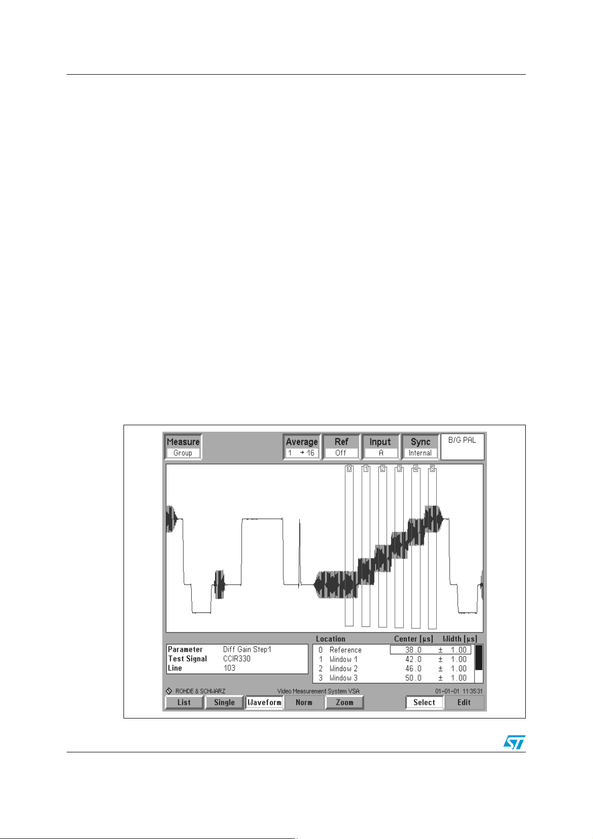
To characterize the differential phase and differential gain a CCIR330 video line is used.
The video line contains five (flat) levels of luminance onto which the chrominance signal is
superimposed. The luminance gives various amplitudes which define the saturation of the
signal. The chrominance gives various phases which define the color of the signal.
Differential phase (or differential gain) distortion is present if a signal chrominance phase
(gain) is affected by the luminance level. The differential phase and gain represent the ability
to uniformly process the high frequency information at all luminance levels.
When a differential gain is present, color saturation is not correctly reproduced.
The input generator is the Rohde & Schwarz CCVS. The output measurement is done by
the Rohde and Schwarz VSA.
Figure 32. Measurement on Rohde and Schwarz VSA
Doc ID 9413 Rev 6 19/29

Test conditions TSH80, TSH81, TSH82, TSH84
Table 7. Video results
Parameter Value (VCC= ±2.5 V) Value (VCC= ±5V) Unit
Lum NL 0.1 0.3 %
Lum NL Step1 100 100 %
Lum NL Step2 100 99.9 %
Lum NL Step3 99.9 99.8 %
Lum NL Step4 99.9 99.9 %
Lum NL Step5 99.9 99.7 %
Diff Gain pos 0 0 %
Diff Gain neg -0.7 -0.6 %
Diff Gain pp 0.7 0.6 %
Diff Gain Step1 -0.5 -0.3 %
Diff Gain Step2 -0.7 -0.6 %
Diff Gain Step3 -0.3 -0.5 %
Diff Gain Step4 -0.1 -0.3 %
Diff Gain Step5 -0.4 -0.5 %
Diff Phase pos 0 0.1 Degree
Diff Phase neg -0.2 -0.4 Degree
Diff Phase pp 0.2 0.5 Degree
Diff Phase Step1 -0.2 -0.4 Degree
Diff Phase Step2 -0.1 -0.4 Degree
Diff Phase Step3 -0.1 -0.3 Degree
Diff Phase Step4 0 0.1 Degree
Diff Phase Step5 -0.2 -0.1 Degree
20/29 Doc ID 9413 Rev 6

TSH80, TSH81, TSH82, TSH84 Precautions on asymmetrical supply operation
4 Precautions on asymmetrical supply operation
The TSH8x device can be used with either a dual or a single supply. If a single supply is
used, the inputs are biased to the mid-supply voltage (+V
carefully designed so as to reject any noise present on the supply rail.
As the bias current is 15 µA, you should use a high resistance R1 (approximately 10 kΩ) to
avoid introducing an offset mismatch at the amplifier’s inputs.
Figure 33. Asymmetrical supply schematic diagram
Cin
IN
+
R2
R3
Vcc+
C3
C2
C1
R1
-
Cf
R4
/2). This bias network must be
CC
Cout
OUT
R5
RL
AM00845
C1, C2, C3 are bypass capacitors intended to filter perturbations from V
. The following
CC
capacitor values are appropriate.
C1 = 100 nF and C2 = C3 = 100 µF
R2 and R3 are such that the current through them must be superior to 100 times the bias
current. Therefore, you could use the following resistance values.
R2=R3=4.7kΩ
C
(R
in
and C
, C
out
are chosen to filter the DC signal by the low pass filters (R1, Cin) and
out
). With R1 = 10 kΩ, R
out
out=RL
= 150 Ω, and Cin=2µF, C
= 220 µF the cutoff
out
frequency obtained is lower than 10 Hz.
Figure 34. Use of the TSH8x in a gain = -1 configuration
IN
R1
R2
R3
C1
C3
C2
-
+
OUT
AM00846
Doc ID 9413 Rev 6 21/29

Package information TSH80, TSH81, TSH82, TSH84
5 Package information
In order to meet environmental requirements, ST offers these devices in different grades of
ECOPACK
specifications, grade definitions and product status are available at: www.st.com. ECOPACK
is an ST trademark.
®
packages, depending on their level of environmental compliance. ECOPACK
22/29 Doc ID 9413 Rev 6

TSH80, TSH81, TSH82, TSH84 Package information
5.1 SOT23-5 package information
Figure 35. SOT23-5 package outline
Table 8. SOT23-5 package mechanical data
Dimensions
Symbol
Millimeters Inches
Min. Typ. Max. Min. Typ. Max.
A 0.90 1.20 1.45 0.035 0.047 0.057
A1 0.15 0.006
A2 0.90 1.05 1.30 0.035 0.041 0.051
B 0.35 0.40 0.50 0.013 0.015 0.019
C 0.09 0.15 0.20 0.003 0.006 0.008
D 2.80 2.90 3.00 0.110 0.114 0.118
D1 1.90 0.075
e 0.95 0.037
E 2.60 2.80 3.00 0.102 0.110 0.118
F 1.50 1.60 1.75 0.059 0.063 0.069
L 0.10 0.35 0.60 0.004 0.013 0.023
3/4
K0° 10°
Doc ID 9413 Rev 6 23/29

Package information TSH80, TSH81, TSH82, TSH84
5.2 SO-8 package information
Figure 36. SO-8 package outline
Table 9. SO-8 package mechanical data
Dimensions
Symbol
Min. Typ. Max. Min. Typ. Max.
A 1.75 0.069
A1 0.10 0.25 0.004 0.010
A2 1.25 0.049
b 0.28 0.48 0.011 0.019
c 0.17 0.23 0.007 0.010
D 4.80 4.90 5.00 0.189 0.193 0.197
E 5.80 6.00 6.20 0.228 0.236 0.244
E1 3.80 3.90 4.00 0.150 0.154 0.157
e 1.27 0.050
h 0.25 0.50 0.010 0.020
L 0.40 1.27 0.016 0.050
Millimeters Inches
3/
L1 1.04 0.040
k1° 8°1° 8°
ccc 0.10 0.004
24/29 Doc ID 9413 Rev 6

TSH80, TSH81, TSH82, TSH84 Package information
5.3 TSSOP8 package information
Figure 37. TSSOP8 package outline
433/0
Table 10. TSSOP8 package mechanical data
Dimensions
Symbol
Millimeters Inches
Min. Typ. Max. Min. Typ. Max.
A 1.20 0.047
A1 0.05 0.15 0.002 0.006
A2 0.80 1.00 1.05 0.031 0.039 0.041
b 0.19 0.30 0.007 0.012
c 0.09 0.20 0.004 0.008
D 2.90 3.00 3.10 0.114 0.118 0.122
E 6.20 6.40 6.60 0.244 0.252 0.260
E1 4.30 4.40 4.50 0.169 0.173 0.177
e 0.65 0.0256
k0° 8°0° 8°
L 0.45 0.60 0.75 0.018 0.024 0.030
L1 1 0.039
aaa 0.10 0.004
Doc ID 9413 Rev 6 25/29

Package information TSH80, TSH81, TSH82, TSH84
5.4 TSSOP14 package information
Figure 38. TSSOP14 package outline
Table 11. TSSOP14 package mechanical data
Dimensions
Symbol
Min. Typ. Max. Min. Typ. Max.
A 1.20 0.047
A1 0.05 0.15 0.002 0.004 0.006
A2 0.80 1.00 1.05 0.031 0.039 0.041
b 0.19 0.30 0.007 0.012
c 0.09 0.20 0.004 0.0089
D 4.90 5.00 5.10 0.193 0.197 0.201
E 6.20 6.40 6.60 0.244 0.252 0.260
E1 4.30 4.40 4.50 0.169 0.173 0.176
e 0.65 0.0256
L 0.45 0.60 0.75 0.018 0.024 0.030
L1 1.00 0.039
k0° 8°0° 8°
Millimeters Inches
433/0
aaa 0.10 0.004
26/29 Doc ID 9413 Rev 6
TSH80, TSH81, TSH82, TSH84 Ordering information
6 Ordering information
Table 12. Order codes
(1)
Temperature
range
-40 to +85 °C
Package Packaging Marking
SOT23-5
SOT23-5
(Automotive grade level)
SO-8
(Automotive grade level)
Tape and reel
Tube or
tape and reel
K303
K310
TSH80I
SH80IY
Type
TSH80ILT
TSH80IYLT
(1)
TSH80ID/DT SO-8
TSH80IYD/IYDT
TSH81ID/DT SO-8 TSH81I
TSH81IPT TSSOP8 Tape and reel SH81I
TSH82ID/DT SO-8
Tube or
tape and reel
TSH82I
TSH82IPT TSSOP8 Tape and reel SH82I
TSH84IPT TSSOP14 Tape and reel SH84I
1. Qualification and characterization according to AEC Q100 and Q003 or equivalent, advanced screening
according to AEC Q001 and Q 002 or equivalent are ongoing.
Doc ID 9413 Rev 6 27/29
Revision history TSH80, TSH81, TSH82, TSH84
7 Revision history
Table 13. Document revision history
Date Revision Changes
1-Feb-2003 1 First release.
2-Aug-2005 2
12-Apr-2007 3
24-Oct-2007 4
19-May-2009 5
24-Jul-2012 6
PPAP references inserted in the datasheet, see Table 12: Order
codes on page 27.
Corrected temperature range for TSH80IYD/IYDT and
TSH82IYD/IYDT order codes in Table 12: Order codes on page 27.
TSH81IYPT PPAP references inserted in the datasheet, see
Table 12: Order codes on page 27.
Added data relating to the quad TSH84 device.
Removed TSH81IYPT, TSH81IYD-IYDT, TSH82IYPT and
TSH82IYD-IYDT order codes in Table 12: Order codes.
Added TSSOP14 package to figure on page 1, updated titles of
Figure 1 to Figure 30, updated Section 5: Package information,
removed TSH80ID-IDT, TSH80IYD, TSH81ID-IDT and TSH82ID
order codes fromTable 12: Order codes. Modified note 1 below
Table 12: Order codes, minor corrections throughout document.
28/29 Doc ID 9413 Rev 6

TSH80, TSH81, TSH82, TSH84
y
Please Read Carefully:
Informatio n in this document is provided solely in connection with ST products. STMicroelectronics NV and its subsidiaries (“ST”) reserve the
right to make changes, corrections, modifications or improvements, to this document, and the products and services described herein at an
time, without notice.
All ST products are sold pursuant to ST’s terms and conditions of sale.
Purchasers are solely responsible for the choice, selection and use of the ST products and services described herein, and ST assumes no
liability whatsoever relating to the choice, selection or use of the ST products and services described herein.
No license, express or imp lied, by estoppel or otherwise, to any intellectual property rights is granted under this do cument. If any part of this
document refers to any third party products or services it shall not be deemed a license grant by ST for the use of such third party products
or services, or any intellectual property contained therein or considered as a warranty covering the use in any manner whatsoever of such
third party products or services or any intellectual property contained therein.
UNLESS OTHERWISE SET FORTH IN ST’S TERMS AND CONDITIONS OF SALE ST DISCLAIMS ANY EXPRESS OR IMPLIED
WARRANTY WITH RESPECT TO THE USE AND/OR SALE OF ST PRODUCTS INCLUDING WITHOUT LIMITATION IMPLIED
WARRANTIES OF MERCHANTABILITY, FITNESS FOR A PARTICULAR PURPOSE (AND THEIR EQUIVALENTS UNDER THE LAWS
OF ANY JURISDICTION), OR INFRINGEMENT OF ANY PATENT, COPYRIGHT OR OTHER INTELLECTUAL PROPERTY RIGHT.
UNLESS EXPRESSLY APPROVED IN WRITING BY TWO AUTHORIZED ST REPRESENTATIVES, ST PRODUCTS ARE NOT
RECOMMENDED, AUTHORIZED OR WARRANTED FOR USE IN MILITARY, AIR CRAFT, SPACE, LIFE SAVING, OR LIFE SUSTAINING
APPLICATIONS, NOR IN PRODUCTS OR SYSTEMS WHERE FAILURE OR MALFUNCTION MAY RESULT IN PERSONAL INJURY,
DEATH, OR SEVERE PROPERTY OR ENVIRONMENTAL DAMAGE. ST PRODUCTS WHICH ARE NOT SPECIFIED AS "AUTOMOTIVE
GRADE" MAY ONLY BE USED IN AUTOMOTIVE APPLICATIONS AT USER’S OWN RISK.
Resale of ST products with provisions different from the statements and/or technical features set forth in this document shall immediately void
any warranty granted by ST for the ST product or service described herein and shall not create or extend in any manner whatsoever, any
liability of ST.
ST and the ST logo a re trademarks or registered trademarks of ST in various countries.
Information in this document supersedes and replaces all information previously supplied.
The ST logo is a registered trademark of STMicroelectronics. All other names are the property of their respective owners.
© 2012 STMicroelectronics - All rights reserved
STMicroelectronics group of companies
Australia - Belgium - Brazil - Canada - China - Czech Republic - Finland - France - Germany - Hong Kong - India - Israel - Italy - Japan -
Malaysia - Malta - Morocco - Philippines - Singapore - Spain - Sweden - Switzerland - United Kingdom - United States of America
www.st.com
Doc ID 9413 Rev 6 29/29
 Loading...