

TSH690
40MHz to 1GHz AMPLIFIER
■ Supply voltage: 1.5V to 5V
■ >20 mW adjustable output power
■ 28 dB gain at 450 MHz
■ 21 dB gain at 900 MHz
■ 50 Ω matched input and output
■ Bias pin to adjust the amplification class
■ Power down
DESCRIPTION
The TSH690 is a wide band RF amplifier, designed in advanced bi polar process. At 450 MHz,
it features 28dB gain and +13.5dBm (20 mW) output power at 3V. At 900 MHz, it features 23 dB
gain and +15.5 dBm (35 mW) output power at 3V.
The pin 8 allows a bias current adjust, setting t he
RF output level and the am plifier be haviour. I t allows using the TSH690 from the linear A-class
trough the AB-class to power-down mode.
The TSH690 is suited to drive power amplifiers in
cellular phones (GSM, TDMA) for which the
’turn-on time’ is controlled by a voltage ramp.
The more than 20 m W output power makes the
TSH690 dedicated as output stage for 433MHz
and 868 MHz ISM transmitters.
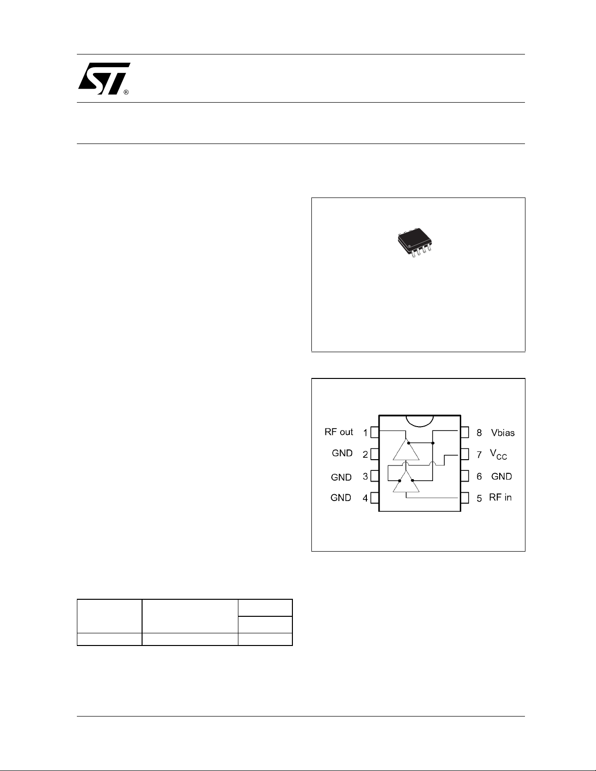
PACKAGE
D
SO8
(Plastic Micropackage)
PIN CONNECTIONS (top view)
APPLICATIONS
■ 433 MHz and 868 MHz ISM transmitters
■ Telemetering systems
■ Remote controls
■ Cordless T elephones
■ Driver for cellular phones
■ Wide band applications
ORDER CODE
Part Number Temperature Range
TSH690ID -40, +85°C
D = Small Outline Package (SO) - also available in Tape & Reel (DT)
March 2001
Package
D
•
1/14

TSH690
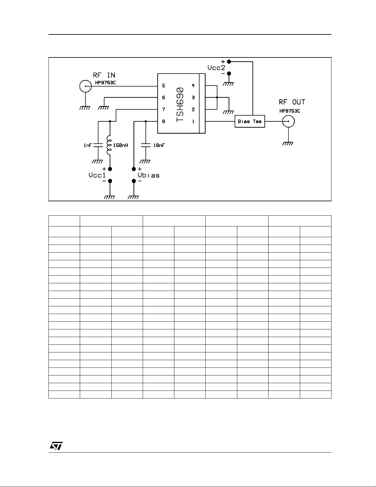
SCHEMATIC DIAGRAM
ABSOLUTE MAXIMUM RATINGS
Symbol Parameter Value Unit
V
, V
CC1
CC2
, V
Supply Voltage & Bias Voltage 5.5 V
bias
RF in RF Input Power +10 dBm
RF out RF Output Power +21 dBm
T
oper
T
stg
Operating Free Air Temperature Range -40 to +85 °C
Storage Temperature Range -65 to +150 °C
OPERATING CONDITIONS
Symbol Parameter Value Unit
V
CC1
V
RF
, V
bias
CC2
sr
Supply Voltages 1.5 to 5 V
Bias Voltage 0 to 5 V
RF Signal Range 40 to 1000 MHz
ESD SENSITIVE DEVICE
Handling Precautions Required
2/14

TSH690
Tj - T
amb
= Pd • R
th(j-a)
ELECTRICAL DC CHARACTERISTICS
Tamb = 25°C, V
Supply Current
Vcc = 2V
Vcc = 2.7V
Vcc = 3V
Vcc = 4V
Vcc = 5V
Rth-(j-a): Junction Ambient Thermal Resistance for SO-8 Package 140 180 °C/W
connected to V
CC
, ZL = 50Ω (unless otherwise specified)
bias
Parameter Min. Typ. Max. Unit
29
33
46
53
mA
79
105
TSH690 DISSIPATION CONSIDERATIONS
In order to respect t he d issipat ion limitati on of the
package, you should co nsider the f ollo wing eq uation:
with:
R
= junction ambient thermal resistance
th(j-a)
T
(°C) = max. junction temperature (150°C)
j
(°C) = ambient temperature
T
amb
(W) = maxi mu m dissi pa ted power
P
d
The respect of this condition forms a safe area on
the following figure:
Figure 1 : Dissipation capability vs T ambient
900
V
800
700
600
500
(mW)
MAX
400
Pd
300
200
100
0
-40-30-20-100 102030405060708090
SAFE
AREA
T
(°C)
AMB
= V
BIAS
CC
RTH = 180°C/W
If VBIAS is DC connected to VCC, the operating
temperature can be directly determined without
determining ICC, thanks to the direct reading
curve:
Figure 2 : Maximu m T
160
140
120
100
(°C)
80
AMB
T
60
40
20
0
0123456
SAFE
AREA
amb
vs V
VCC(V)
CC
V
BIAS=VCC
R
THmax
=180°C/W
In applications using a duty cycle, the average dissipation is less than in continuous mode. The following figure gives the relation beetween the dissipated power and the duty cycle.
Figure 3 : Dissipation vs Duty cycle
900
Pd = VCC x ICC x Duty Cycle
800
700
600
500
400
Pd(mW)
300
200
100
0
0 102030405060708090100
Duty Cycle(%)
VCC = 5V
VCC = 4V
VCC = 3V
VCC = 2V
3/14

TSH690
ELECTRICAL CHARACTERISTICS AT 450 MHz
Tamb = 25°C, V
Power gain S21 (P
Output Power 1dB Compression 8 12 dBm
3rd Order Intercept Point (f = 430MHz) 16 22 dBm
Reverse Isolation S12 (f = 400MHz) -46 dB
Input Return Loss S11 -10 -15 dB
Noise Figure 4.5 dB
1. All min. and m ax. parameters of this table are garanteed by co rrelation with 900 MHz t ests.
ELECTRICAL CHARACTERISTICS AT 900 MHz
Tamb = 25°C, V
Power gain S21 (P
Output Power at 1dB compression point +12 +14.3 dBm
Output power, Pin = -7 dBm +10 +11.7 dBm
3rd Order Intercept Point +25 dBm
Reverse Isolation S12 -35 dB
Input Return Loss S11 -14 dB
Output Return Loss S22 -4.5 dB
Noise figure 5.4 dB
1. All min. and m ax. parameters of this table are garanteed by te st .
& V
CC
= -20dBm)
in
& V
CC
= -20dBm)
in
= +2.7V, ZL = 50Ω, f = 450 MHz (unless otherwise specified)
bias
Parameter
1)
Min. Typ. Max. Unit
20 23 30 dB
= +3V, ZL = 50Ω, f = 900 MHz (unless otherwise specified)
bias
Parameter
1)
Min. Typ. Max. Unit
19 21 dB
4/14
TSH690
SCATTERING PARAMETERS MEASUREMENT (Reference waves planes at package leads)
TEST CONDITIONS V
CC1
, V
CC2
, V
= +2V, P i n = -40dBm, T
bias
= 25°C
amb
Freq S11 S21 S12 S22
MHz Mag Ang Mag Ang Mag Ang Mag Ang
40 0.642 -22.0 6.319 5.0 0.003 -126.5 0.715 -54.7
50 0.615 -25.7 6.406 7.1 0.008 170.7 0.631 -64.7
100 0.537 -41.3 7.643 7.7 0.002 70.1 0.369 -91.3
150 0.490 -55.6 9.353 3.1 0.004 -141.9 0.253 -100.9
200 0.464 -68.0 11.502 -5.7 0.007 -117.3 0.202 -100.9
250 0.428 -79.0 13.856 -18.0 0.003 162.3 0.203 -92.7
300 0.413 -92.1 16.229 -33.4 0.005 142.1 0.209 -87.6
350 0.373 -101.5 18.019 -51.2 0.008 101.4 0.263 -89.4
400 0.334 -106.7 19.110 -70.1 0.008 115.2 0.326 -99.7
450 0.312 -111.5 19.159 -90.3 0.008 169.9 0.382 -112.1
500 0.290 -112.5 18.154 -108.0 0.008 111.5 0.395 -122.9
550 0.302 -114.5 16.778 -124.8 0.010 92.1 0.425 -130.0
600 0.324 -118.2 15.075 -140.5 0.015 93.6 0.424 -139.6
650 0.335 -122.9 13.482 -153.6 0.011 109.6 0.427 -150.8
700 0.349 -129.6 11.992 -165.5 0.011 101.7 0.425 -159.0
750 0.368 -135.0 10.750 -177.2 0.019 82.4 0.414 -169.5
800 0.366 -142.1 9.453 173.4 0.011 79.5 0.413 -177.8
850 0.373 -147.9 8.598 165.0 0.015 60.2 0.432 176.2
900 0.374 -154.1 7.783 155.8 0.013 89.7 0.438 166.4
950 0.381 -159.0 7.117 146.7 0.017 111.3 0.447 160.8
1000 0.377 -165.8 6.500 138.9 0.013 82.2 0.462 155.1
5/14
 Loading...