

Features
■ Selectable 6th order filtering of 36 MHz,
18 MHz and 9 MHz
■ 5 V single-supply operation
■ Internal input DC level shifter
■ No input capacitor required
■ 3 matched 6 dB amplifiers
■ AC or DC output-coupled
■ Very low harmonic distortion
■ Specified for 150 Ω loads
■ Data min. and max. are tested during
production
Applications
■ High-end video systems
■ High definition TV (HDTV)
■ Broadcast and graphic video
■ Multimedia products
Description
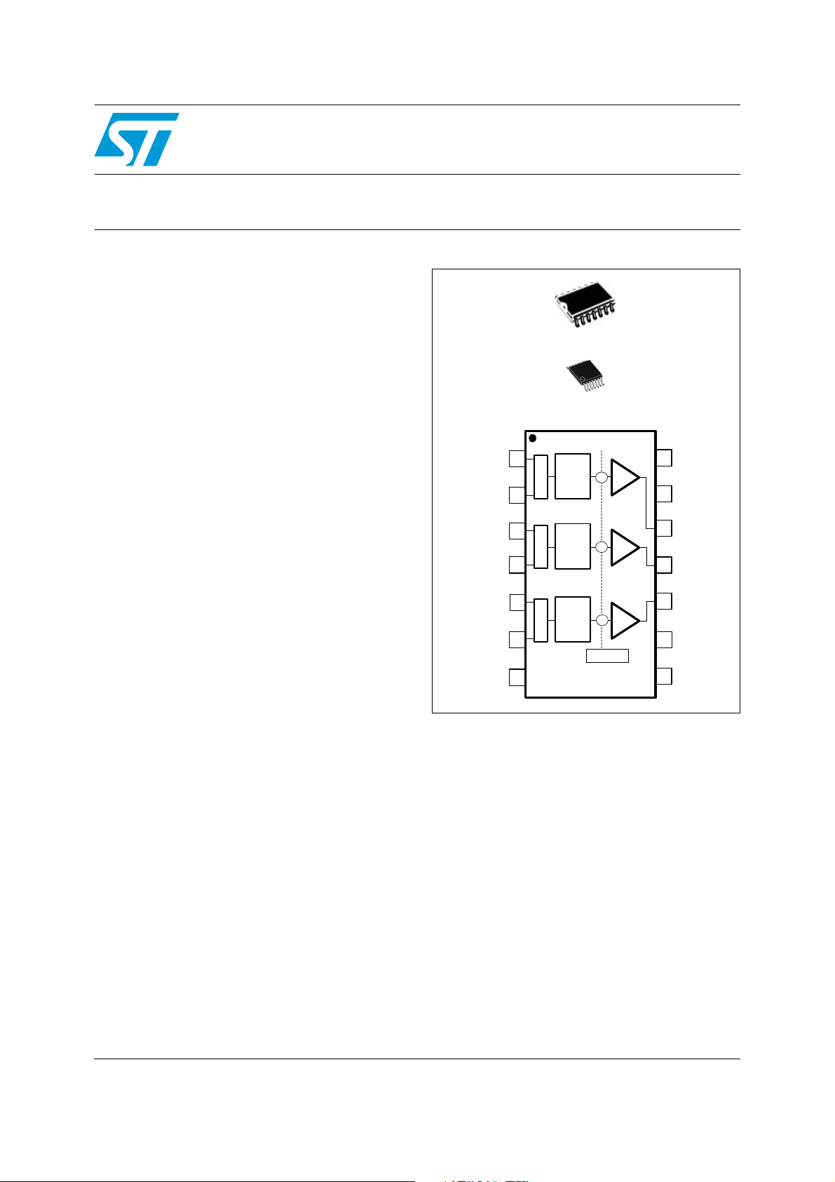
TSH345
Triple video buffer with selectable filter
for HD and SD video applications
SO-14
TSSOP14
Fs0
R1 in
R2 in
G1 in
G2 in
B1 in
B2 in
+VCC
1
2
3
4
5
6
7
MUX
MUXMUX
36MHz
18MHz
9MHz
LPF
36MHz
18MHz
9MHz
LPF
36MHz
18MHz
9MHz
LPF
+
+
+
DC Shifter
6dB
6dB
6dB
14
13
12
11
10
Fs1
R out
G out
B out
Mux
9
GND
8
The TSH345 is a triple single-supply video buffer
featuring an internal gain of 6 dB and selectable
filtering for HD and SD video outputs on 75 Ω
video lines. The TSH345 is ideal to drive YC,
CVBS, YUV, YPbPr or RGB signals from video
DAC outputs.
The main advantage of this circuit is its input DC
level shifter. It allows driving video signals on 75 Ω
video lines without damaging the synchronization
tip and without input or output capacitors when
using a single 5 V power supply. The DC level
shifter is internally fixed and optimized to keep the
output video signals between low and high output
rails in the best position for the greatest linearity.
The TSH345 is available in SO-14 and TSSOP-14
plastic packages for optimum space saving.
December 2008 Rev 1 1/23
www.st.com
23
Absolute maximum ratings and operating conditions TSH345
1 Absolute maximum ratings and operating conditions
Table 1. Absolute maximum ratings
Symbol Parameter Value Unit
V
T
T
CC
V
oper
stg
T
Supply voltage
in
Input voltage range 2.5 V
Operating free air temperature range -40 to +85 °C
Storage temperature -65 to +150 °C
Maximum junction temperature 150 °C
j
(1)
6V
Thermal resistance junction to case
R
thjc
SO-14
TSSOP14
22
32
Thermal resistance junction to ambient area
R
thja
P
max
ESD
SO-14
TSSOP14
Maximum power dissipation (at T
SO-14
TSSOP14
CDM: charged device model
HBM: human body model
MM: machine model
=25°C) for Tj= 150° C
amb
125
110
1
1.1
250
2
100
°C/W
°C/W
W
V
kV
V
1. All voltage values, except differential voltage, are with respect to network terminal.
Table 2. Operating conditions
Symbol Parameter Value Unit
V
CC
1. Tested in full production with +5 V single power supply.
Power supply voltage 4.5 to 5.5
(1)
V
2/23
TSH345 Electrical characteristics
2 Electrical characteristics
Table 3. Electrical characteristics at VCC= +5 V single supply, T
(unless otherwise specified)
Symbol Test conditions Min. Typ. Max. Unit
DC performance
Output DC shift
V
DC
= 150 Ω, T
R
L
-40° C < T
Input bias current
I
ib
T
, input to GND
amb
-40° C < T
R
C
Input resistance, T
in
Input capacitance, T
in
Total supply current (3 x operators)
I
CC
No load, input to GND
-40°C < T
DC voltage gain
G
= 150Ω, Vin=1.4V
R
L
-40°C < T
Output characteristics
amb
amb
amb
amb
amb
< +85° C
< +85° C
amb
amb
<+85°C
<+85°C
100 240
44.64551.6 mA
1.96 2
1.96
=25°C
amb
440 mV
310
1.3
3.6 µA
1.4
1MΩ
0.1 pF
2.05 V/V
V
OH
V
OL
I
out
Filtering
Standard
definition
High level output voltage
= 150 Ω
R
L
-40° C < T
amb
< +85° C
Low level output voltage
RL= 150 Ω
I
source
T
amb
-40° C < T
I
sink
-40° C < T
amb
amb
< +85° C
< +85° C
Bandwidth
F1 selected, small signal, V
=0.5V, RL=150Ω
ICM
-3 dB bandwidth
-1 dB bandwidth
Attenuation
F1 selected/F=27 MHz, small signal, V
=150Ω
R
L
ICM
=0.5V,
3.4 3.9
3.8
47 mV
76 100
91
106 134
126
9
5
5.7
MHz
40 45 dB
V
mA
mA
3/23
Electrical characteristics TSH345
Table 3. Electrical characteristics at VCC= +5 V single supply, T
amb
=25°C
(unless otherwise specified) (continued)
Symbol Test conditions Min. Typ. Max. Unit
Bandwidth
Standard
definition
with
progressive
scanning
F2 selected, small signal, V
-3 dB bandwidth
-1 dB bandwidth
Attenuation
F2 selected/F = 54 MHz, small signal,
V
=0.5V, RL=150Ω
ICM
Bandwidth
F3 selected, small signal, V
High
definition
-3 dB bandwidth
-1 dB bandwidth
Attenuation
F3 selected/F = 74.25 MHz, small signal,
V
=0.5V, RL=150Ω
ICM
D Delay between each channel 0.5 ns
gd
Δg
ΔΦ
Group delay variation
F1 selected/F = 0 to 6 MHz
Differential gain
F1 selected/F = 6 MHz, R
Differential phase
F1 selected/F = 6 MHz, R
Noise
=0.5V, RL= 150 Ω
ICM
=0.5V, RL= 150 Ω
ICM
=150Ω
L
=150Ω
L
21
13
18
32 38 dB
36
25
32
25 32 dB
11 ns
0.38 %
0.5 °
MHz
MHz
Total input voltage noise in Standard Definition
F = 100 kHz, RIN=50Ω
eN
Total input voltage noise in High Definition
F = 100 kHz, R
IN
=50Ω
Standby mode
Total current consumption in standby mode
I
STBY
T
T
on
off
Fs1 = 1, Fs0 = 1
T
amb
-40° C < T
amb
< +85° C
Time from standby to active mode 5 µs
Time from active to standby mode 5 µs
Fs1, Fs0 and Mux features
V
V
high
low
High level 0.9 V
Low level 0.3 V
4/23
74
86
440
480
690
nV/√Hz
µA
TSH345 Electrical characteristics
Table 4. Filter and standby settings, VCC= +5 V single supply, T
(1)
Fs1
0 0 F3 Filtering for high definition (HD)
0 1 F2 Filtering for progressive video (PV)
1 0 F3 Filtering for standard definition (SD)
1 1 Standby TSH345 in standby mode
1. Fs1 and Fs0 pins must never be left floating.
Table 5. Mux settings, VCC= +5 V single supply, T
(1)
Mux
0 R1 G1 B1 Video1 selected
1 R2 G2 B2 Video2 selected
1. The MUX pin must never be left floating.
Fs0
(1)
Settings
amb
Settings
=25°C
amb
=25°C
5/23
Electrical characteristics TSH345
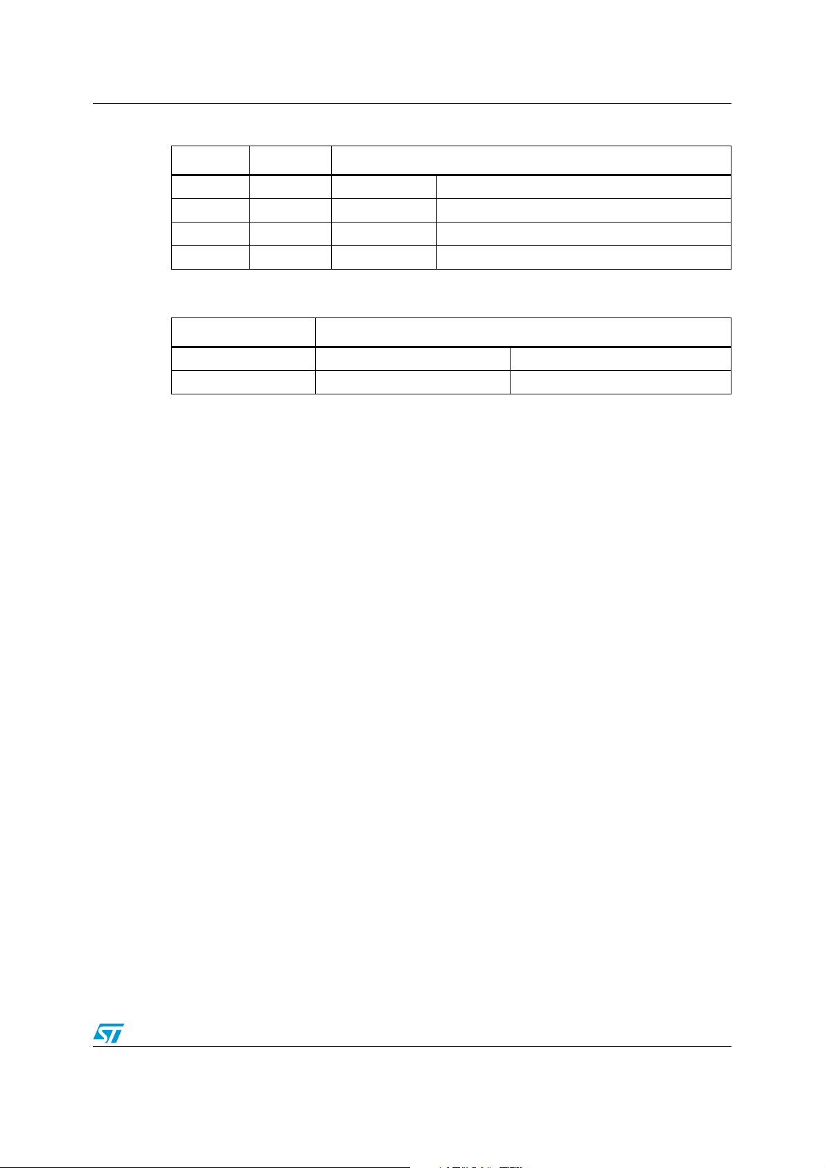
Figure 1. Filtering Figure 2. Gain flatness
10
0
-10
-20
SD
-30
HD
PV
Filter response (dB)
Vcc=5V
-40
small signal
Load=150
-50
1M 10M 100M
Ω
Frequency (Hz)
6.2
6.0
5.8
5.6
Filter response (dB)
5.4
5.2
Vcc=5V
small signal
Load=150
SD
Ω
1M 10M
Frequency (Hz)
Figure 3. Distortion 1 MHz (HD) Figure 4. Distortion 10 MHz (HD)
0
Vcc=5V
-10
F=1MHz
-20
HD filter
Load=150
-30
-40
-50
-60
-70
HD2 & HD3 (dBc)
-80
-90
-100
0.00.51.01.52.02.53.03.54.0
Ω
HD2
HD3
Output Amplitude (Vp-p)
0
Vcc=5V
-10
F=10MHz
-20
HD filter
Load=150
-30
-40
-50
-60
-70
HD2 & HD3 (dBc)
-80
-90
-100
0.0 0.5 1.0 1.5 2.0 2.5 3.0 3.5 4.0
Ω
HD2
HD3
Output Amplitude (Vp-p)
HD
PV
Figure 5. Distortion 1 MHz (PV) Figure 6. Distortion 10 MHz (PV)
0
Vcc=5V
-10
F=1MHz
PV filter
-20
Load=150
-30
-40
-50
-60
-70
HD2 & HD3 (dBc)
-80
-90
-100
0.00.51.01.52.02.53.03.54.0
Ω
HD2
HD3
Output Amplitude (Vp-p)
6/23
0
Vcc=5V
-10
F=10MHz
PV filter
-20
Load=150
-30
-40
-50
-60
-70
HD2 & HD3 (dBc)
-80
-90
-100
0.0 0.5 1.0 1.5 2.0 2.5 3.0 3.5 4.0
Ω
HD2
HD3
Output Amplitude (Vp-p)
TSH345 Electrical characteristics
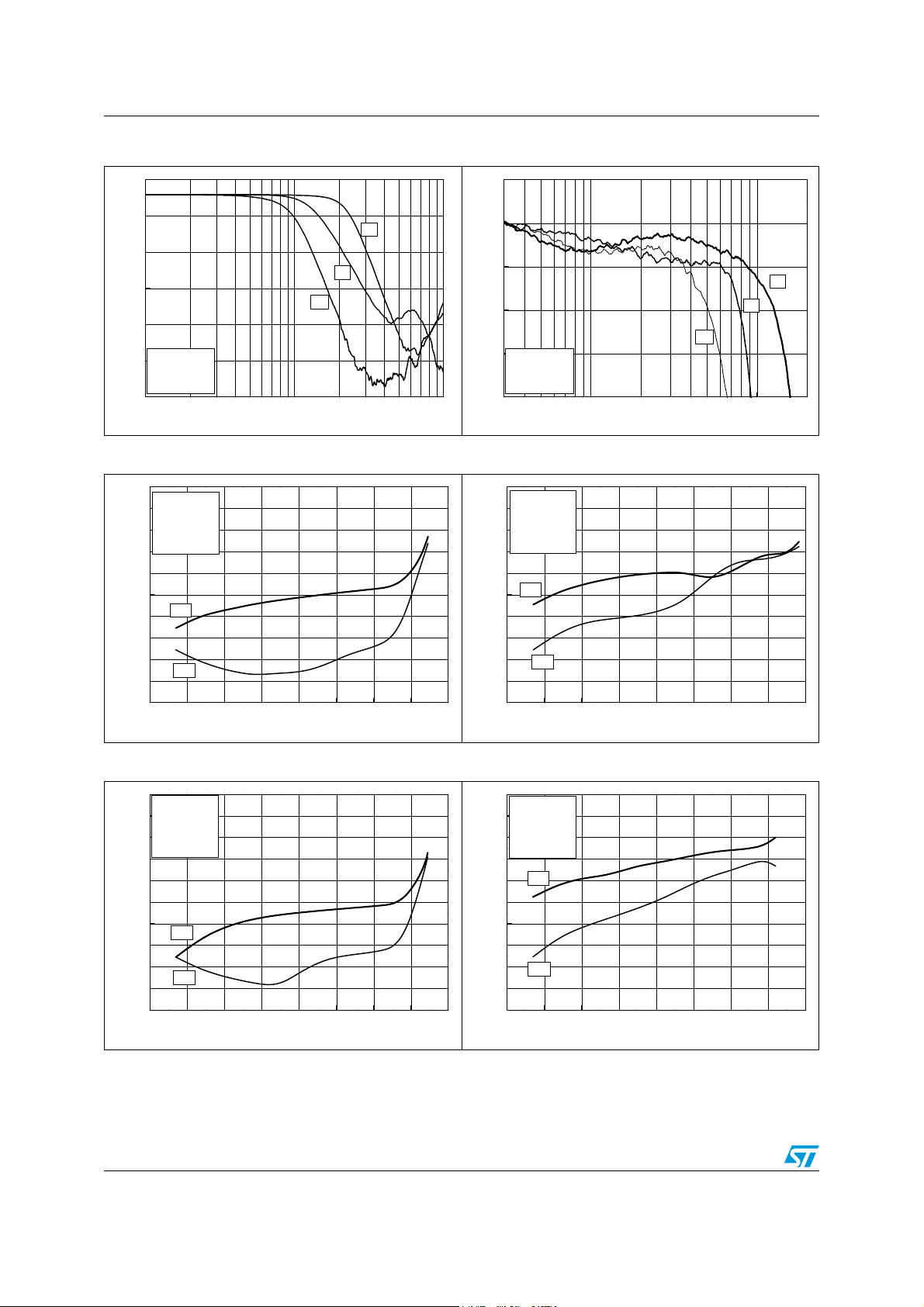
Figure 7. Distortion 1 MHz (SD filter) Figure 8. Input noise vs. frequency
0
Vcc=5V
-10
F=1MHz
SD filter
-20
Load=150
-30
-40
-50
-60
-70
HD2 & HD3 (dBc)
-80
-90
-100
0.00.51.01.52.02.53.03.54.0
Ω
HD2
HD3
Output Amplitude (Vp-p)
1000
HD
PV
SD
100
Input Noise (nV/VHz)
100 1k 10k 100k 1M
Frequency (Hz)
Vcc=5V
No load
Figure 9. Gain vs. input amplitude Figure 10. Channel crosstalk vs. frequency
Gain (V/V)
2.10
2.05
2.00
1.95
Vcc=5V
Load=150
Ω
X-Talk (dB)
-40
-45
-50
-55
-60
-65
-70
Input: 1Vp-p
HD filter
Vcc=5V
Load=150
Ω
1.90
0.0 0.2 0.4 0.6 0.8 1.0 1.2 1.4
Vin (Vp-p)
-75
1M 10M 100M
Frequency (Hz)
Figure 11. Output vs input amplitude Figure 12. MUX isolation
5.0
Vcc=5V
4.5
Load=150
4.0
3.5
3.0
2.5
2.0
Vout (V)
1.5
1.0
0.5
0.0
0.0 0.2 0.4 0.6 0.8 1.0 1.2 1.4 1.6 1.8 2.0
Ω
Output DCshift
V
OH
Vin (V)
-40
Input: 1Vp-p
Vcc=5V
-45
Load=150
-50
-55
-60
-65
MUX isolation (dB)
-70
-75
1M 10M 100M
Ω
Frequency (Hz)
7/23

Electrical characteristics TSH345
Icc
(mA)
Figure 13. Current consumption vs. supply Figure 14. Supply current vs. temperature
Vcc=5V
no Load
40
30
20
10
0
0.0 0.5 1.0 1.5 2.0 2.5 3.0 3.5 4.0 4.5 5.0
Vcc (V)
50
Vcc=5V
49
no Load
48
47
46
45
(mA)
CC
44
I
43
42
41
40
-40-20 0 20406080
Temperature (°C)
Figure 15. Filtering vs. temperature Figure 16. Filter attenuation vs. temperature
40
Vcc=5V
35
Load=150
30
25
20
15
10
-1dB Bandwidth (MHz)
5
0
-40-200 20406080
Ω
Temperature (°C)
HD
PV
SD
60
Vcc=5V
55
Load=150
50
45
PV, f=54MHz
40
35
Attenuation (dB)
30
25
20
-40-20 0 20406080
Ω
SD, f=27MHz
HD, f=74.25MHz
Temperature (°C)
Figure 17. Gain matching vs. temperature Figure 18. Output DC shift vs. temperature
5
Vcc=5V
Load=150
4
3
2
MG (%)
1
0
-40 -20 0 20 40 60 80
Ω
Temperature (°C)
8/23
400
Vcc=5V
375
Load=150
350
325
300
275
250
225
DCshift (mV)
200
175
150
125
100
-40-20 0 20406080
Ω
Temperature (°C)

TSH345 Electrical characteristics
Figure 19. Standby current vs. temperature Figure 20. Isink vs. temperature
180
Vcc=5V
no Load
170
160
150
Istandby (µA)
140
130
120
-40 -20 0 20 40 60 80
Temperature (°C)
150
140
130
120
110
100
90
Isink (mA)
80
70
60
Vcc=5V
50
-40-20 0 20406080
Temperature (°C)
Figure 21. Isource vs. temperature Figure 22. Ibias vs. temperature
120
110
100
90
80
Isource (mA)
70
60
Vcc=5V
50
-40-200 20406080
Temperature (°C)
2.0
Vcc=5V
1.8
1.6
1.4
1.2
1.0
(μA)
BIAS
0.8
I
0.6
0.4
0.2
0.0
-40-200 20406080
Temperature (°C)
Figure 23. VOL vs. temperature Figure 24. VOH vs. temperature
60
55
50
45
VOL (mV)
40
35
Vcc=5V
Load=150
30
-40-200 2040 6080
Ω
Temperature (°C)
4.00
3.95
3.90
3.85
3.80
VOH (V)
3.75
3.70
3.65
Vcc=5V
Load=150
3.60
-40-20 0 20406080
Ω
Temperature (°C)
9/23

Electrical characteristics TSH345
Figure 25. Gain vs. temperature
2.20
2.15
2.10
2.05
2.00
Gain (dB)
1.95
1.90
1.85
Vcc=5V
Load=150
1.80
-40 -20 0 20 40 60 80
Ω
Temperature (°C)
10/23

TSH345 Electrical characteristics
2.1 Power supply considerations: improving the power supply noise rejection
Correct power supply bypassing is very important to optimize performance in low- and highfrequency ranges. Bypass capacitors should be placed as close as possible to the IC pin
(pin 4) to improve high-frequency bypassing. A capacitor (C
necessary to improve the PSRR in low frequencies. For better quality bypassing, you can
add a capacitor of 100 nF (C
HF
). C
must be placed as close as possible to the IC pin to
HF
improve the noise supply rejection in the higher frequencies. A coil can be added in order to
better reject the noise from the supply and to prevent current peaks as much as possible.
Figure 26. Circuit for power supply bypassing
+V
CC
Coil
+
) greater than 10 µF is
LF
C
LF
C
HF
7
R
G
B
TSH345
8
AM00816
11/23

Electrical characteristics TSH345
T
Figure 27. Circuit for noise rejection improvement measurement
S
R
+5 V
T-bias
50 7
TSH345
+
C
LF
50 7
AGILEN
4395A
A
AM00817
Coil
C
HF
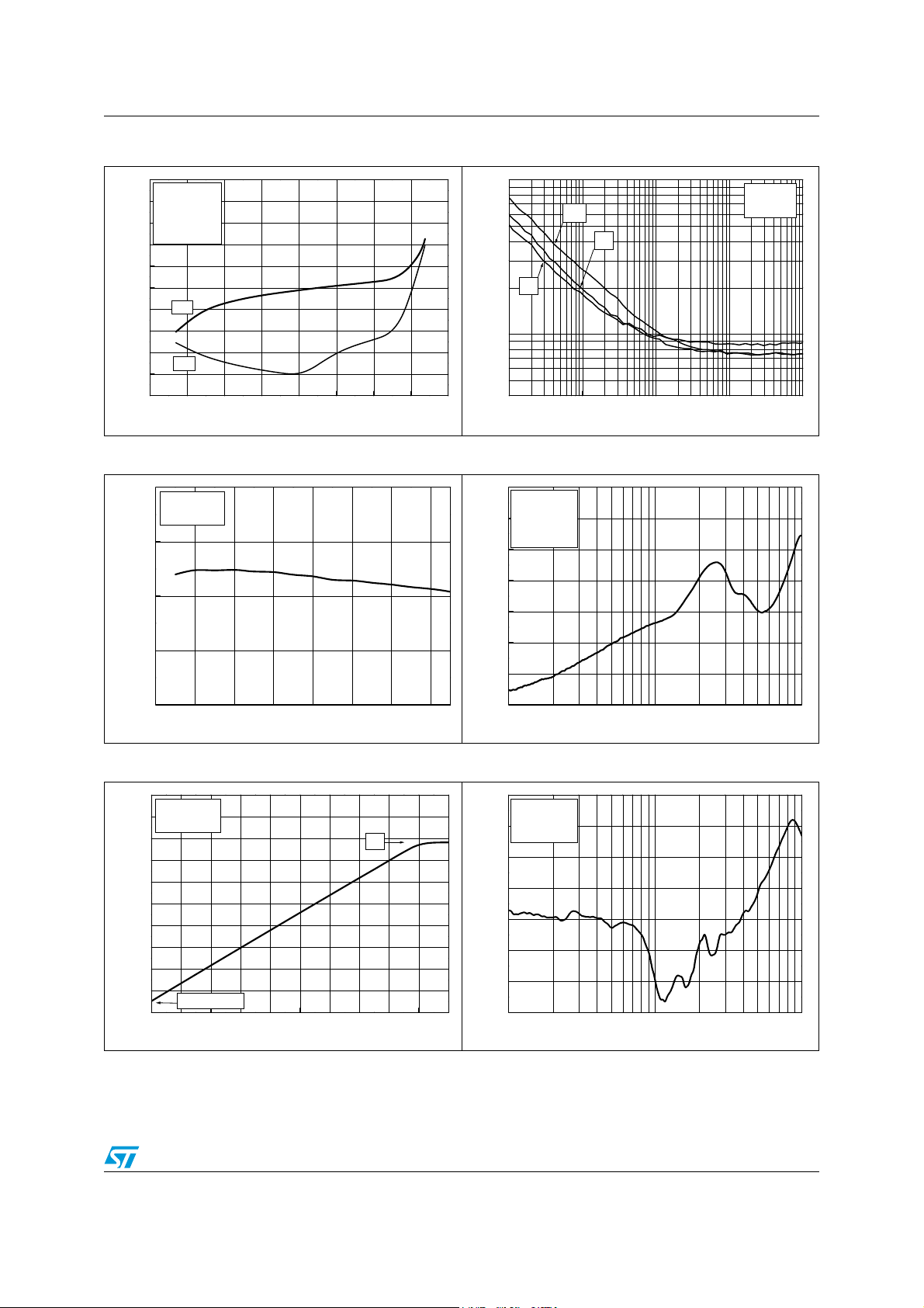
Figure 28 shows how the power supply noise rejection evolves according to the frequency
and depending on how carefully power supply decoupling is achieved.
Figure 28. Power supply noise rejection
0
Vcc=5V(dc)+0.2Vp-p(ac)
-10
Decoupling capacitor: 10µF+100nF
Load=150
Noise rejection=20 log (ΔVCC/ΔVout)
-20
Ω
-30
-40
-50
-60
Noise rejection ratio (dB)
-70
coil=560µH
-80
10k 100k 1M 10M 100M
12/23
no coil
Frequency (Hz)

TSH345 Using the TSH345 to drive YC, CVBS, YUV, YPbPr and RGB video components
DAC
DAC
DAC
3 Using the TSH345 to drive YC, CVBS, YUV, YPbPr and
RGB video components
Figure 29. Implementation of the video driver on output video DACs
+5 V
Reconstruction
filtering
LPF
Reconstruction
filtering
LPF
+
+ 6 dB
+
+
+
+ 6 dB
75 7
2 Vpp
75 7
1.4 Vpp1.
75 7cable
75 7cable
1 Vpp
75 7
0.7 Vpp
75 7
TV
Video
Video
Y
1 Vpp
Pb
0.7 Vpp0.
Video
0.7 Vpp0.
Pr
Reconstruction
filtering
LPF
+
+
-5 V
+ 6 dB
TSH345
GND
75 7
1.4 Vpp1.
75 7cable
.
0
75 7
7 Vpp
AM00818
13/23

Using the TSH345 to drive YC, CVBS, YUV, YPbPr and RGB video components TSH345
14.8 u
24.3 u
clock
1/
Figure 30. Synchronization details (example for a black picture)
HD
GND
SD
GND
300 mV
300 mV
27 ns
(2t)
590 ns
160 ns
54 ns
(44 t)
sync.tip
4.6 us
(4t)
590 ns
(44 t)
150 ns
sync.tip
27 ns
(2t)
300 mV
•F
•t=
=74.25 MHz
Fclock=13.5 ns
Black (30IRE)
s(1100t): 1920/1080i
s(1800t): 1280/720i
Black (30IRE)
64 us
Figure 31. HD video signal
300 mV
GND
DAC’s offset
(DAC’s offset on STi7200 = 28 mV)
AM00819
Video contents up to 30 MHz
1 Vp-p (+/- 5 %)
AM00820
14/23

TSH345 Using the TSH345 to drive YC, CVBS, YUV, YPbPr and RGB video components
Figure 32. Standard video signal
Video contents up to 6 MHz
1.3 Vp-p (+/- 5 %)
300 mV
GND
DAC’s offset
(DAC’s offset on STi7200 = 28 mV)
AM00821
15/23

Using the TSH345 to drive YC, CVBS, YUV, YPbPr and RGB video components TSH345
Figure 33. Flexibility of the TSH345 for SD and HD signals
HD/PV/SD
Y,G
DAC
Pb,B,C
DAC
Pr,R,CVBS
DAC
HD/PV/SD
Y,G
DAC
Pb,B,C
DAC
Pr,R,CVBS
DAC
150Ω
150Ω
NC
150Ω
150Ω
150Ω
150Ω
MUX and Filter select
(as defined in Table 4
and Table 5)
150Ω
150Ω
150Ω
150Ω
150Ω
150Ω
NC
NC
NC
NC
NC
+5V
TSH345
TSH345
TSSOP14
TSSOP14
SO14
SO14
+5V
TSH345
TSH345
TSSOP14
TSSOP14
SO14
SO14
75Ω
75Ω
75Ω
75Ω
75Ω
75Ω
RCA
Cable
Cable
Cable
R-G-B
Y-Pb-Pr
Y-C-C
SCART
VBS
Cable
Cable
Cable
75Ω
75Ω
75Ω
75Ω
75Ω
75Ω
75Ω
75Ω
75Ω
75Ω
75Ω
75Ω
Y-C
TV
RCA
C
TV
VBS
MUX and Filter select
(as defined in Table 4
and Table 5)
The TSH345 is used to drive either high-definition video signals up to 30 MHz or progressive
and interlaced standard definition video signals on 75-Ω video lines. It can drive a large
panel of signals such as YC and CVBS, YUV, YPbPr and RGB, where the bottom of the
signal (the synchronization tip in the case of Y and CVBS signals) is close to zero volts. An
internal input DC value is added to the video signal in order to shift the bottom from GND.
The shift is not based on the average of the signal, but is an analog summation of a DC
component to the video signal. Therefore, no input capacitors are required, which provides a
real advantage in terms of cost and board space.
Under these conditions, it is possible to drive the signal in single supply without any
saturation of the driver against the lower rail.
Since half of the signal is lost through output impedance matching, in order to properly drive
the video line the shifted signal is multiplied by a gain of 2 or +6 dB.
16/23

TSH345 Using the TSH345 to drive YC, CVBS, YUV, YPbPr and RGB video components
3.1 Output capacitor
The output can be either DC-coupled or AC-coupled. The output can be directly connected
to the line via a 75-Ω resistor (see Figure 34), or an output capacitor can be used to remove
any DC components in the load. Assuming the load is 150 Ω, a coupling capacitor of 220 µF
can be used to provide a very low cut-off frequency close to 5 Hz (see Figure 35).
Figure 34. DC output coupling for SD, PV and HD
+5V
Video
DAC
150 7
Figure 35. AC output coupling
75 7
TSH345
75 7cable
75 7
AM00822
+5V
Video
DAC
TSH345
75 7
150 7
1. CS is 100 nF used to decrease the parasitic components of C in high frequencies. It is preferable to limit the
use of this output AC-coupling to the standard definition only.
2. The 75-Ω resistor must be as close as possible to the output of the driver to minimize the effect of parasitic
capacitance.
C=220 µF
+
C
S
75 7 cable
75 7
AM00823
17/23

Package information TSH345
4 Package information
In order to meet environmental requirements, ST offers these devices in different grades of
ECOPACK
specifications, grade definitions and product status are available at: www.st.com.
ECOPACK
®
packages, depending on their level of environmental compliance. ECOPACK®
®
is an ST trademark.
18/23

TSH345 Package information
4.1 SO-14 package information
Figure 36. SO-14 package mechanical drawing
Table 6. SO-14 package mechanical data
Dimensions
Millimeters Inches
Ref.
Min. Typ. Max. Min. Typ. Max.
A 1.35 1.75 0.05 0.068
A1 0.10 0.25 0.004 0.009
A2 1.10 1.65 0.04 0.06
B 0.33 0.51 0.01 0.02
C 0.19 0.25 0.007 0.009
D 8.55 8.75 0.33 0.34
E 3.80 4.0 0.15 0.15
e1.27 0.05
H 5.80 6.20 0.22 0.24
h 0.25 0.50 0.009 0.02
L 0.40 1.27 0.015 0.05
k 8° (max.)
ddd 0.10 0.004
Note: D and F dimensions do not include mold flash or protrusions. Mold flash or protrusions must
not exceed 0.15 mm.
19/23

Package information TSH345
4.2 TSSOP14 package information
Figure 37. TSSOP14 package mechanical drawing
Table 7. TSSOP14 package mechanical data
Dimensions
Ref.
Min. Typ. Max. Min. Typ. Max.
A1.200.047
A1 0.05 0.15 0.002 0.004 0.006
A2 0.80 1.00 1.05 0.031 0.039 0.041
b 0.19 0.30 0.007 0.012
c 0.09 0.20 0.004 0.0089
D 4.90 5.00 5.10 0.193 0.197 0.201
E 6.20 6.40 6.60 0.244 0.252 0.260
E1 4.30 4.40 4.50 0.169 0.173 0.176
e 0.65 0.0256
L 0.45 0.60 0.75 0.018 0.024 0.030
L1 1.00 0.039
k0° 8°0° 8°
aaa 0.10 0.004
Millimeters Inches
20/23

TSH345 Ordering information
5 Ordering information
Table 8. Order codes
Part number
TSH345ID
TSH345IDT Tape & reel TSH345I
TSH345IPT TSSOP14 Tape & reel TSH345I
Temperature
range
-40°C to +85°C
Package Packing Marking
SO-14
Tube TSH345I
21/23

Revision history TSH345
6 Revision history
Table 9. Document revision history
Date Revision Changes
29-May-2007 1 Initial release.
18-Dec-2008 2
Added curves in Chapter 2: Electrical characteristics.
Added all test limits in Chapter Table 3.
22/23

TSH345
Please Read Carefully:
Information in this document is provided solely in connection with ST products. STMicroelectronics NV and its subsidiaries (“ST”) reserve the
right to make changes, corrections, modifications or improvements, to this document, and the products and services described herein at any
time, without notice.
All ST products are sold pursuant to ST’s terms and conditions of sale.
Purchasers are solely responsible for the choice, selection and use of the ST products and services described herein, and ST assumes no
liability whatsoever relating to the choice, selection or use of the ST products and services described herein.
No license, express or implied, by estoppel or otherwise, to any intellectual property rights is granted under this document. If any part of this
document refers to any third party products or services it shall not be deemed a license grant by ST for the use of such third party products
or services, or any intellectual property contained therein or considered as a warranty covering the use in any manner whatsoever of such
third party products or services or any intellectual property contained therein.
UNLESS OTHERWISE SET FORTH IN ST’S TERMS AND CONDITIONS OF SALE ST DISCLAIMS ANY EXPRESS OR IMPLIED
WARRANTY WITH RESPECT TO THE USE AND/OR SALE OF ST PRODUCTS INCLUDING WITHOUT LIMITATION IMPLIED
WARRANTIES OF MERCHANTABILITY, FITNESS FOR A PARTICULAR PURPOSE (AND THEIR EQUIVALENTS UNDER THE LAWS
OF ANY JURISDICTION), OR INFRINGEMENT OF ANY PATENT, COPYRIGHT OR OTHER INTELLECTUAL PROPERTY RIGHT.
UNLESS EXPRESSLY APPROVED IN WRITING BY AN AUTHORIZED ST REPRESENTATIVE, ST PRODUCTS ARE NOT
RECOMMENDED, AUTHORIZED OR WARRANTED FOR USE IN MILITARY, AIR CRAFT, SPACE, LIFE SAVING, OR LIFE SUSTAINING
APPLICATIONS, NOR IN PRODUCTS OR SYSTEMS WHERE FAILURE OR MALFUNCTION MAY RESULT IN PERSONAL INJURY,
DEATH, OR SEVERE PROPERTY OR ENVIRONMENTAL DAMAGE. ST PRODUCTS WHICH ARE NOT SPECIFIED AS "AUTOMOTIVE
GRADE" MAY ONLY BE USED IN AUTOMOTIVE APPLICATIONS AT USER’S OWN RISK.
Resale of ST products with provisions different from the statements and/or technical features set forth in this document shall immediately void
any warranty granted by ST for the ST product or service described herein and shall not create or extend in any manner whatsoever, any
liability of ST.
ST and the ST logo are trademarks or registered trademarks of ST in various countries.
Information in this document supersedes and replaces all information previously supplied.
The ST logo is a registered trademark of STMicroelectronics. All other names are the property of their respective owners.
© 2008 STMicroelectronics - All rights reserved
STMicroelectronics group of companies
Australia - Belgium - Brazil - Canada - China - Czech Republic - Finland - France - Germany - Hong Kong - India - Israel - Italy - Japan -
Malaysia - Malta - Morocco - Singapore - Spain - Sweden - Switzerland - United Kingdom - United States of America
www.st.com
23/23
 Loading...