

340MHz single-supply triple video buffer
Features
■ Bandwidth: 340MHz
■ 5V single-supply operation
■ Low output rail guaranteed at 60mV max
■ Internal gain of 6dB for a matching between 3
channels
■ Very low harmonic distortion
■ Slew rate: 740V/ms
■ Specified for 150Ω and 100Ω loads
■ Tested on 5V power supply
■ Min. and max. data tested during production
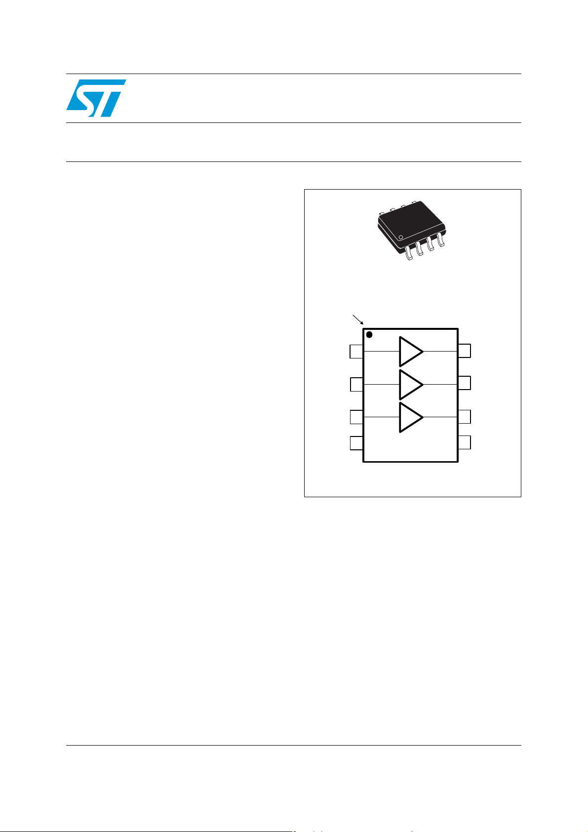
Pin connections (top view)
Pin1 identification
1
IN1
Top View
6dB
TSH344
8
OUT1
Applications
■ High-end video systems
■ High definition TV (HDTV)
■ Broadcast and graphic video
■ Multimedia products
Description
The TSH344 is a triple single-supply video buffer
featuring an internal gain of 6dB and a large
bandwidth of 340MHz.
The main advantage of this buffer is its very low
output rail very close to GND when supplied in
single supply 0/5V. This output rail is guaranteed
by test at 60mV from GND on 150Ω.
datasheet gives technical information on using
the TSH344 as an RGB driver for video DAC
output on a video line. See the TSH343 datasheet
for Y-Pb-Pr signals.
The TSH344 is available in the compact SO8
plastic package for optimum space-saving.
This
IN2
IN3
+Vcc
7
6
5
OUT2
OUT3
GND
2
3
4
6dB
6dB
SO8
March 2007 Rev 4 1/17
www.st.com
17

Contents TSH344
Contents
1 Absolute maximum ratings and operating conditions . . . . . . . . . . . . . 3
2 Electrical characteristics . . . . . . . . . . . . . . . . . . . . . . . . . . . . . . . . . . . . . 4
3 Application information . . . . . . . . . . . . . . . . . . . . . . . . . . . . . . . . . . . . . 10
3.1 Using the TSH344 to drive R-G-B video components . . . . . . . . . . . . . . . 10
3.2 Power supply considerations . . . . . . . . . . . . . . . . . . . . . . . . . . . . . . . . . . 12
3.3 Delay between channels . . . . . . . . . . . . . . . . . . . . . . . . . . . . . . . . . . . . . 13
4 Package information . . . . . . . . . . . . . . . . . . . . . . . . . . . . . . . . . . . . . . . . 14
5 Ordering information . . . . . . . . . . . . . . . . . . . . . . . . . . . . . . . . . . . . . . . 16
6 Revision history . . . . . . . . . . . . . . . . . . . . . . . . . . . . . . . . . . . . . . . . . . . 16
2/17
TSH344 Absolute maximum ratings and operating conditions
1 Absolute maximum ratings and operating conditions
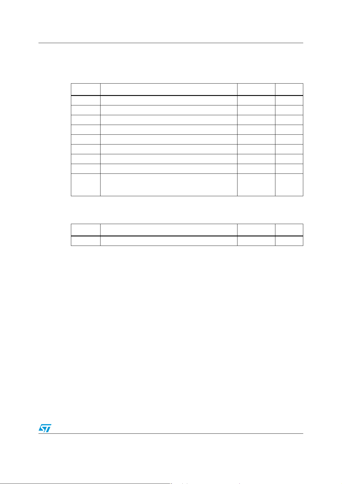
Table 1. Absolute maximum ratings (AMR)
Symbol Parameter Value Unit
V
T
T
R
R
P
CC
V
oper
stg
T
thjc
thja
max
Supply voltage
Input voltage range
in
Operating free air temperature range -40 to +85 °C
Storage temperature -65 to +150 °C
Maximum junction temperature 150 °C
j
SO8 thermal resistance junction to case 28 °C/W
SO8 thermal resistance junction to ambient area 157 °C/W
Maximum power dissipation (@T
CDM: charged device model
ESD
HBM: human body model
MM: machine model
1. All voltage values, except differential voltage, are with respect to network terminal.
2. The magnitude of input and output voltage must never exceed VCC +0.3V.
Table 2. Operating conditions
(1)
(2)
6V
0 to +2 V
=25°C) for Tj=150°C 800 mW
amb
2
1.5
200
kV
kV
V
Symbol Parameter Value Unit
V
CC
1. Tested in full production at 0V/5V single power supply.
Power supply voltage
(1)
3 to 5.5 V
3/17
Electrical characteristics TSH344
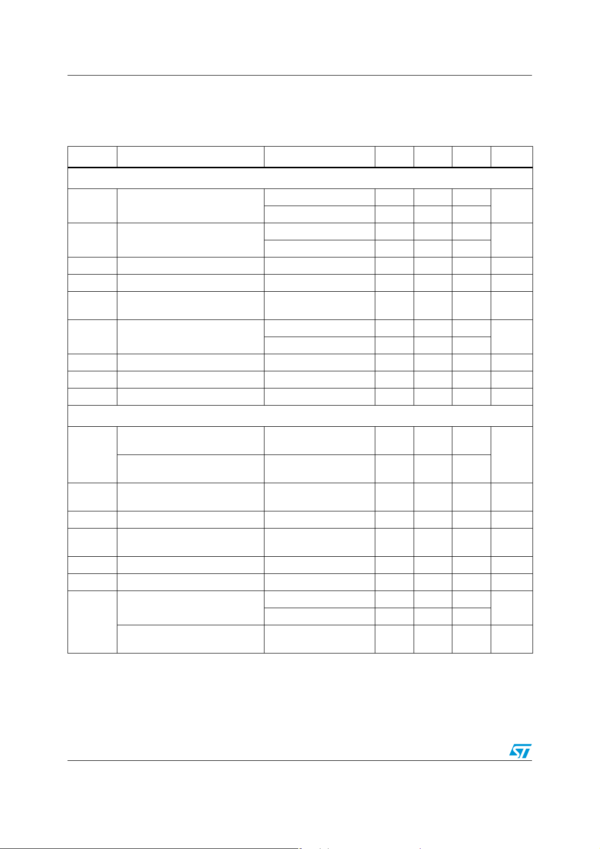
2 Electrical characteristics
Table 3. VCC= +5V single supply, T
= 25°C (unless otherwise specified)
amb
Symbol Parameter Test conditions Min. Typ. Max. Unit
DC performance
V
OS
I
ib
R
in
C
in
PSRR
Output offset voltage
(1)
Input bias current
Input resistance T
Input capacitance T
Power supply rejection ratio
20 log (
ΔV
CC
/ΔV
out
(2)
)
No load, T
-40°C < T
T
, input to GND 5.5 16
amb
-40°C < T
amb
amb
Input to GND, F=1MHz,
ΔV
=200mV
CC
-35 -8 +35
amb
< +85°C -8.6
amb
< +85°C 6
amb
4GΩ
1pF
-90 dB
No load, input to GND 10.1 13
CC Supply current per buffer
I
G DC v oltage gain R
-40°C < T
= 150Ω, Vin=1V 1.92 2 2.05 V/V
L
< +85°C 10.3
amb
MG1 Gain matching between 3 channels Input = 1V 0.5 2 %
MG0.3 Gain matching between 3 channels Input = 0.3V 0.5 2 %
Dynamic performance and output characteristics
mV
μA
mA
-3dB bandwidth
Bw
Gain flatness @ 0.1dB
FPBW Full power bandwidth
Small signal V
V
=0.6V, RL = 150Ω
icm
Small signal V
V
=0.6V, RL = 150Ω
icm
=0.6V, V
V
icm
= 150Ω
R
L
=20mVp
out
=20mVp
out
= 2Vp-p,
out
190 340
65
130 200 MHz
D Delay between each channel 0 to 30MHz 0.5 ns
V
SR Slew rate
V
V
High level output voltage RL = 150Ω 3.7 3.9 V
OH
Low level output voltage RL = 150Ω 40 60 mV
OL
Output current
I
OUT
Output short circuit current
)
(I
source
(3)
=0.6V, V
icm
= 150Ω
R
L
= 2Vp, T
V
out
-40°C < T
= 2Vp-p,
out
amb
< +85°C 83
amb
500 740 V/μs
45 93
100 mA
MHz
mA
4/17
TSH344 Electrical characteristics
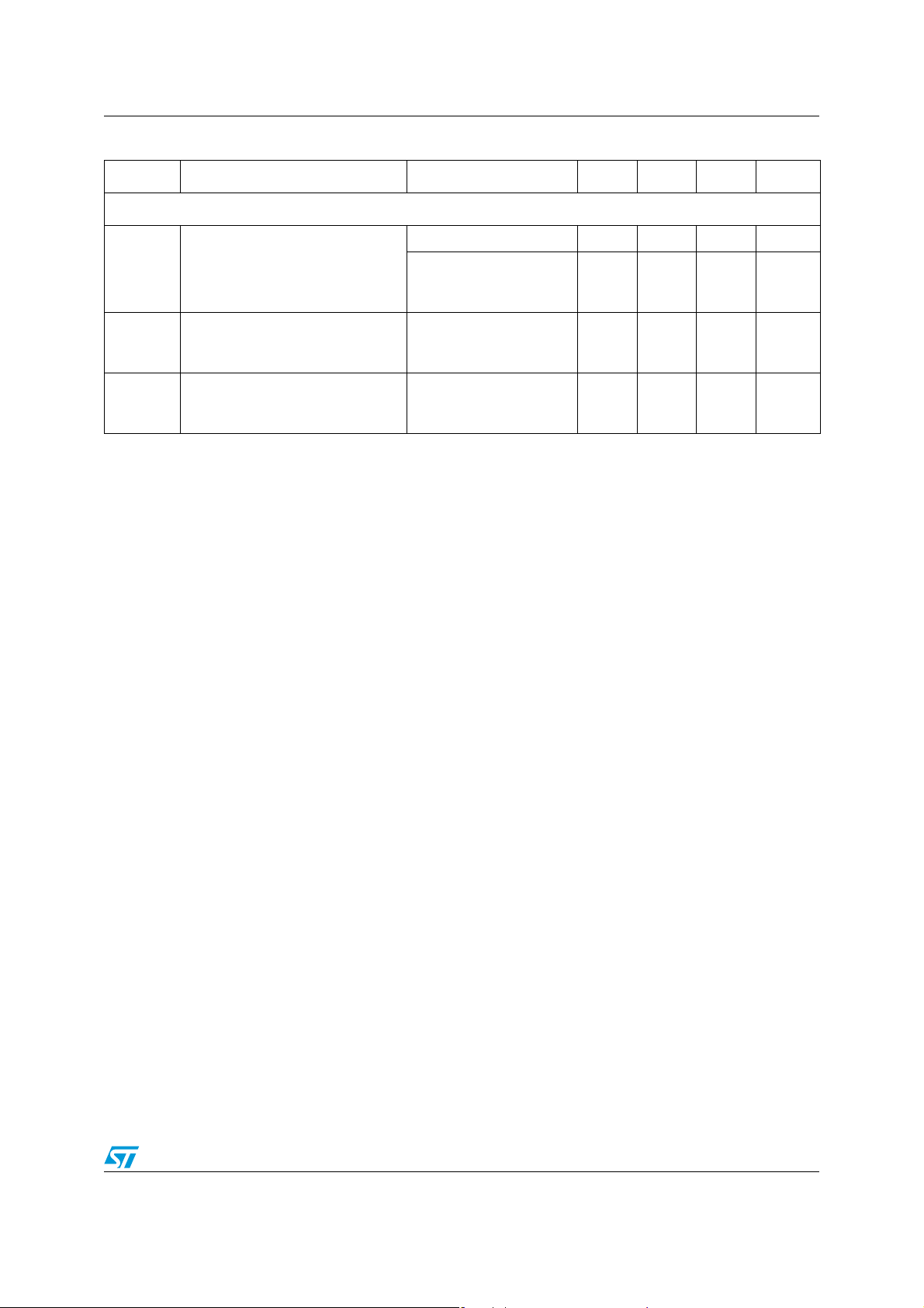
Table 3. VCC= +5V single supply, T
= 25°C (unless otherwise specified)
amb
Symbol Parameter Test conditions Min. Typ. Max. Unit
Noise and distortion
F = 100kHz, R
R
= 50Ω
eN Total input voltage noise
in
Bw=30MHz
Bw=100MHz
= 2Vp-p, RL = 150Ω
V
out
HD2 2nd harmonic distortion
F= 10MHz
F= 30MHz
V
= 2Vp-p, RL = 150Ω
HD3 3rd harmonic distortion
out
F= 10MHz
F= 30MHz
1. Output offset voltage is determined by the following expression: V
2. See Figure28 and Figure 29.
3. Non-tested value, guaranteed by design and evaluation. See Figure12.
= 50Ω 8nV/√Hz
in
55
100
-57
-42
-72
-51
=G.VIN+VOS.
OUT
μVrms
dBc
dBc
5/17
Electrical characteristics TSH344
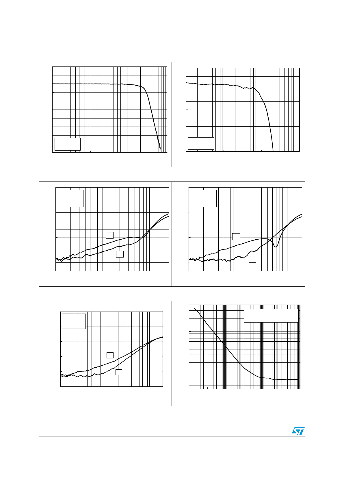
Figure 1. Frequency response Figure 2. Gain flatness
10
8
6
4
2
0
-2
Gain (dB)
-4
-6
Vcc=5V
-8
Load=150
-10
1M 10M 100M 1G
Ω
Frequency (Hz)
6,2
6,1
6,0
5,9
5,8
5,7
5,6
Gain (dB)
5,5
5,4
Vcc=5V
5,3
Load=150
5,2
1M 10M 100M 1G
Ω
Frequency (Hz)
Figure 3. Cross-talk vs. frequency (amp1) Figure 4. Cross-talk vs. frequency (amp2)
0
Small Signal
-10
Vcc=5V
Load=150
-20
-30
-40
-50
-60
Gain (dB)
-70
-80
-90
-100
1M 10M 100M
Ω
1/2
1/3
Frequency (Hz)
0
Small Signal
Vcc=5V
Load=150
-20
-40
-60
Gain (dB)
-80
Ω
2/1
2/3
-100
1M 10M 100M
Frequency (Hz)
Figure 5. Cross-talk vs. frequency (amp3) Figure 6. Input noise vs. frequency
0
Small Signal
Vcc=5V
Load=150
-20
-40
-60
Gain (dB)
-80
-100
1M 10M 100M
Ω
3/1
3/2
Frequency (Hz)
6/17
100
Input Noise (nV/VHz)
10
10 100 1k 10k 100k 1M 10M
Frequency (Hz)
Vcc=5V
DC input = 1.5V (Battery)
 Loading...