

TS4909
Dual mode low power 150mW stereo headphone amplifier
with capacitor-less and single-ended outputs
Features
■ No output coupling capacitors necessary
■ Pop-and-click noise reduction circuitry
■ Operating from V
■ Standby mode active low
■ Output power:
= 2.2V to 5.5V
CC
– 158mW @5V, into 16Ω with 1% THD+N
max (1kHz)
– 52mW @3.0V into 16Ω with 1% THD+N
max (1kHz)
■ Ultra low current consumption: 2.0mA typ.@3V
■ Ultra low standby consumption: 10nA typ.
■ High signal-to-noise ratio: 105 dB typ.@5V
■ High crosstalk immunity: 110dB (F=1kHz) for
single-ended outputs
■ PSRR: 72dB (F=1kHz), inputs grounded, for
phantom ground outputs
■ Low t
■ Available in lead-free DFN10 3x3mm
: 50ms in PHG mode, 100ms in SE mode
WU
Applications
■ Headphone amplifier
■ Mobile phone
■ PDA, portable audio player
Description
The TS4909 is a stereo audio amplifier designed
to drive headphones in portable applications.
The integrated phantom ground is a circuit
topology that eliminates the heavy output coupling
capacitors. This is of primary importance in
portable applications where space constraints are
very high. A single-ended configuration is also
available, offering even lower power consumption
because the phantom ground can be s witched off.
DFN10 (3x3)
Pin connections (top view)
Vin1
Stdby
SE/PHG
Bypass
Vin2
1
1
2
2
3
3
4
4
5
5
10
10
Vdd
9
9
Vout1
8
8
Vout3
7
7
Vout2
6
6
Gnd
Functional block diagram
SE/PHG
Vout1
Vout3
Vout2
Vin1
Stdby
Bypass
Vin2
Vdd
BIAS
Gnd
Pop-and-click noise during switch-on and switchoff phases is eliminated by integrated circuitry.
Specially designed for applications requiring low
power supplies, the TS4909 is capable of
delivering 31mW of continuous average power
into a 32Ω load with less than 1% THD+N from a
3V power supply.
Featuring an active low standby mode, the
TS4909 reduces the supply current to only 10nA
(typ.). The TS4909 is unity ga in stable an d can be
configured by external gain-setting resistors.
September 2007 Rev 8 1/32
www.st.com
32

Contents TS4909
Contents
1 Typical application schematics . . . . . . . . . . . . . . . . . . . . . . . . . . . . . . . . 3
2 Absolute maximum ratings and operating conditions . . . . . . . . . . . . . 4
3 Electrical characteristics . . . . . . . . . . . . . . . . . . . . . . . . . . . . . . . . . . . . . 5
4 Application information . . . . . . . . . . . . . . . . . . . . . . . . . . . . . . . . . . . . . 22
4.1 General description . . . . . . . . . . . . . . . . . . . . . . . . . . . . . . . . . . . . . . . . . 22
4.2 Frequency response . . . . . . . . . . . . . . . . . . . . . . . . . . . . . . . . . . . . . . . . . 22
4.3 Gain using the typical application schematics . . . . . . . . . . . . . . . . . . . . . 23
4.4 Power dissipation and efficiency . . . . . . . . . . . . . . . . . . . . . . . . . . . . . . . 24
4.4.1 Single-ended configuration . . . . . . . . . . . . . . . . . . . . . . . . . . . . . . . . . . 24
4.4.2 Phantom ground configuration . . . . . . . . . . . . . . . . . . . . . . . . . . . . . . . . 25
4.4.3 Total power dissipation . . . . . . . . . . . . . . . . . . . . . . . . . . . . . . . . . . . . . . 26
4.5 Decoupling of the circuit . . . . . . . . . . . . . . . . . . . . . . . . . . . . . . . . . . . . . . 26
4.6 Wake-up time . . . . . . . . . . . . . . . . . . . . . . . . . . . . . . . . . . . . . . . . . . . . . . 27
4.7 Pop performance . . . . . . . . . . . . . . . . . . . . . . . . . . . . . . . . . . . . . . . . . . . 27
4.8 Standby mode . . . . . . . . . . . . . . . . . . . . . . . . . . . . . . . . . . . . . . . . . . . . . 28
5 Package information . . . . . . . . . . . . . . . . . . . . . . . . . . . . . . . . . . . . . . . . 29
6 Ordering information . . . . . . . . . . . . . . . . . . . . . . . . . . . . . . . . . . . . . . . 31
7 Revision history . . . . . . . . . . . . . . . . . . . . . . . . . . . . . . . . . . . . . . . . . . . 31
2/32
TS4909 Typical application schematics
1 Typical application schematics
Figure 1. Typical applications for the TS4909
Rfeed1
Phantom ground configuration
Vin1
Cin1
330nF
Vin2
330nF
Cin2
Single-ended configuration
20k
20k
Rin1
Standby
Cb
1µF
20k
Rin2
20k
Rfeed2
Rfeed1
20k
BIAS
Vcc
Cs
1µF
Gnd
Vcc
Cs
1µF
SE/PHG
Vout1
Vout3
Vout2
SE/PHG
Vin1
Cin1
20k
Rin1
330nF
Standby
Cb
1µF
Vin2
330nF
20k
Rin2
Cin2
Table 1. Application component information
BIAS
Gnd
20k
Rfeed2
Component Functional description
R
C
R
feed1,2
in1,2
in1,2
C
b
C
s
Inverting input resistor that sets the closed loop gain in conjunction with R
resistor also forms a high pass filter with C
(fc = 1 / (2 x Pi x Rin x Cin)).
in
Input coupling capacitor that blocks the DC voltage at the amplifier’s input term inal.
Feedback resistor that sets the closed loop gain in conjunction with Rin.
= closed loop gain = -R
A
V
feed/Rin
.
Half supply bypass capacitor.
Supply bypass capacitor that provides power supply filtering.
Vout1
Vout3
Vout2
Cout1
Cout2
feed
. This
3/32
Absolute maximum ratings and operating conditions TS4909
2 Absolute maximum ratings and operating conditions
Table 2. Absolute maximum ratings
Symbol Parameter Value Unit
V
CC
V
T
stg
T
R
thja
P
diss
Supply voltage
Input voltage -0.3V to V
i
Storage temperature -65 to +150 °C
Maximum junction temperature 150 °C
j
Thermal resistance junction to ambient DFN10 120 °C/W
Pow e r di ssi p at ion
ESD Human body model (pin to pin) 2 kV
(1)
(2)
DFN10
6V
+0.3V V
CC
1.79 W
ESD
Machine model
220pF - 240pF (pin to pin)
200 V
Latch-up Latch-up immunity (all pins) 200 mA
Lead temperature (soldering, 10 sec) 260 °C
Output current 170
1. All voltage values are measured with respect to the ground pin.
2. Pd is calculated with T
3. Caution: this device is not protected in the event of abnormal operating conditions, such as for example,
short-circuiting between any one output pin and ground, between any one output pin and VCC, and
between individual output pins.
Table 3. Operating conditions
= 25°C, T
amb
junction
= 150°C.
(3)
Symbol Parameter Value Unit
V
T
CC
R
oper
Supply voltage 2.2 to 5.5 V
Load resistor ≥ 16 Ω
L
Operating free air temperature range -40 to + 85 °C
Load capacitor
C
L
= 16 to 100Ω
R
L
R
> 100Ω
L
400
100
Standby voltage input
V
STBY
TS4909 in STANDBY
TS4909 in active state
GND ≤ V
1.35V ≤ V
STBY
STBY
≤ 0.4
≤ V
(1)
CC
Single-ended or phantom ground configuration
V
SE/PHG
R
thja
1. The minimum current consumption (I
2. When mounted on a 4-layer PCB.
voltage Input
TS4909 outputs in single-ended configuration
TS4909 outputs in phantom ground configuration
Thermal resistance junction to ambient DFN10
) is guaranteed at ground for the whole temperature range.
STBY
(2)
V
SE/PHG=VCC
V
SE/PHG
=0
41 °C/W
mA
pF
V
V
4/32

TS4909 Electrical characteristics
3 Electrical characteristics
Table 4. Electrical characteristics at VCC = +5V with GND = 0V and T
amb
= 25°C
(unless otherwise specified)
Symbol Parameter Test conditions Min. Typ. Max. Unit
I
CC
I
STBY
P
out
THD+N
PSRR
I
out
V
O
Supply current
Standby
current
Output power
Total
harmonic
distortion +
noise
=-1)
(A
v
Pow er supply
rejection ratio
Max output
current
Output swing
No input signal, no load, single-ended
No input signal, no load, phantom ground
No input signal, R
THD+N = 1% max, F = 1kHz, R
=32Ω 10 1000 nA
L
= 32Ω, single-ended
L
THD+N = 1% max, F = 1kHz, RL = 16Ω, single-ended
THD+N = 1% max, F = 1kHz, RL = 32Ω, phantom ground
THD+N = 1% max, F = 1kHz, R
RL = 32Ω, P
RL = 16Ω, P
= 32Ω, P
R
L
RL = 16Ω, P
Inputs grounded
V
=200mVpp
ripple
= 60mW, 20Hz ≤ F ≤ 20kHz, single-ended
out
= 90mW, 20Hz ≤ F ≤ 20kHz, single-ended
out
= 60mW , 20Hz ≤ F ≤ 20kHz, phantom ground
out
= 90mW, 20Hz ≤ F ≤ 20kHz, phantom ground
out
(1)
, Av=-1, RL>=16Ω, Cb=1μF, F = 217Hz,
= 16Ω, phantom ground
L
Single-ended output referenced to phantom ground
Single-ended output referenced to ground
THD +N ≤ 1%, R
: RL = 32Ω
V
OL
: RL = 32Ω
V
OH
= 16Ω connected between out and VCC/2 140 mA
L
VOL: RL = 16Ω
VOH: RL = 16Ω
60
95
60
95
666172
4.39
4.17
2.1
3.1
88
158
85
150
0.3
0.3
0.3
0.3
67
0.14
4.75
0.25
4.55
3.2
4.8
0.47
0.69
mA
mW
%
dB
V
A-weighted, A
SNR
Signal-to-
noise ratio
20Hz ≤ F ≤ 20kHz
Single-ended
Phantom ground
R
= 32Ω, Av=-1, phantom ground
L
F = 1kHz
Cross-
talk
Channel
separation
F = 20Hz to 20kHz
= 32Ω, Av=-1, single-ended
R
L
F = 1kHz
F = 20Hz to 20kHz
OO
Output offset
voltage
Wake-up time
Phantom ground configuration, floating inputs, R
Phantom ground configuration
Single-ended configuration
V
t
WU
1. Guaranteed by design and evaluation.
=-1, RL = 32Ω, THD +N < 0.4%,
v
5/32
104
105
-73
-68
-110
-90
=22KΩ 520mV
feed
50
10080160
dB
dB
ms

Electrical characteristics TS4909
Table 5. Electrical characteristics at VCC = +3.0V
with GND = 0V, T
= 25°C (unless otherwise specified)
amb
(1)
Symbol Parameter Test conditions Min. Typ. Max. Unit
I
CC
I
STBY
P
out
THD+N
PSRR
I
out
V
O
Supply current
Standby
current
Output power
T otal harmonic
distortion +
noise
=-1)
(A
v
Power supply
rejection ratio
Max output
current
Output swing
No input signal, no load, single-ended
No input signal, no load, phantom ground
No input signal, R
THD+N = 1% max, F = 1kHz, R
=32Ω 10 1000 nA
L
= 32Ω, single-ended
L
THD+N = 1% max, F = 1kHz, RL = 16Ω, single-ended
THD+N = 1% max, F = 1kHz, R
= 32Ω, phanto m ground
L
THD+N = 1% max, F = 1kHz, RL = 16Ω, phanto m ground
R
= 32Ω, P
L
= 16Ω, P
R
L
RL = 32Ω, P
RL = 16Ω, P
Inputs grounded
V
= 200mVpp
ripple
= 25mW, 20Hz ≤ F ≤ 20kHz, single-ended
out
= 40mW, 20Hz ≤ F ≤ 20kHz, single-ended
out
= 25mW , 20Hz ≤ F ≤ 20kHz, phantom ground
out
= 40mW, 20Hz ≤ F ≤ 20kHz, phantom ground
out
(2)
, Av=-1, RL>=16Ω, Cb=1μF, F = 217 Hz,
Single-ended output referenced to phantom ground
Single-ended output referenced to ground
THD +N ≤ 1%, R
: RL = 32Ω
V
OL
: RL = 32Ω
V
OH
= 16Ω connected between out and VCC/2 82 mA
L
VOL: RL = 16Ω
VOH: RL = 16Ω
2.6
2.45
2.8
20
31
30
52
20
31
30
54
0.3
0.3
0.3
0.3
645970
65
0.12
2.83
0.19
2.70
2
2.8
mA
4.2
mW
0.34
0.49
%
dB
V
=-1, RL = 32Ω, THD +N < 0.4%, 20Hz ≤ F ≤
v
SNR
Signal-to-
noise ratio
A-weighted, A
20kHz
Single-ended
Phantom ground
= 32Ω, Av=-1, phantom ground
R
L
F = 1kHz
Cross-
talk
Channel
separation
F = 20Hz to 20kHz
= 32Ω, Av=-1, single-ended
R
L
F = 1kHz
F = 20Hz to 20kHz
OO
Output offset
voltage
Wake-up time
Phantom ground configuration, floating inputs, R
Phantom ground configuration
Single-ended configuration
feed
V
t
WU
1. All electrical values are guaranteed with correlation measurements at 2.6V and 5V.
2. Guaranteed by design and evaluation.
100
dB
101
-73
-68
dB
-110
-90
=22KΩ 520mV
50
10080160
ms
6/32

TS4909 Electrical characteristics
Table 6. Electrical characteristics at VCC = +2.6V
with GND = 0V, T
Symbol Parameter Test conditions Min. Typ. Max. Unit
= 25°C (unless otherwise specified)
amb
I
CC
I
STBY
P
out
THD+N
PSRR
I
out
V
O
Supply
current
Standby
current
Output power
Total
harmonic
distortion +
noise
=-1)
(A
v
Power supply
rejection ratio
Max output
current
Output swing
No input signal, no load, single-ended
No input signal, no load, phantom ground
No input signal, R
THD+N = 1% max, F = 1kHz, R
=32Ω 10 1000 nA
L
= 32Ω, single-ended
L
THD+N = 1% max, F = 1kHz, RL = 16Ω, single-ended
THD+N = 1% max, F = 1kHz, RL = 32Ω, phantom ground
THD+N = 1% max, F = 1kHz, R
= 32Ω, P
R
L
RL = 16Ω, P
RL = 32Ω, P
= 16Ω, P
R
L
Inputs grounded
V
= 200mVpp
ripple
= 20mW , 20Hz ≤ F ≤ 20kHz, single-ended
out
= 30mW , 20Hz ≤ F ≤ 20kHz, single-ended
out
= 20mW , 20Hz ≤ F ≤ 20kHz, phantom ground
out
= 30mW , 20Hz ≤ F ≤ 20kHz, phantom ground
out
(1)
, Av=-1, RL>=16Ω, Cb=1μF, F = 217Hz,
= 16Ω, phantom ground
L
Single-ended output referenced to phantom ground
Single-ended output referenced to ground
THD +N ≤ 1%, R
: RL = 32Ω
V
OL
: RL = 32Ω
V
OH
= 16Ω connected between out and VCC/2 70 mA
L
VOL: RL = 16Ω
VOH: RL = 16Ω
15
22
15
22
645970
2.25
2.11
1.9
2.8
23
38
23
39
0.3
0.3
0.3
0.3
65
0.11
2.45
0.18
2.32
2.7
4
0.3
0.44
mA
mW
%
dB
V
A weighted, A
SNR
Signal-to-
noise ratio
20Hz ≤ F ≤ 20kHz
Single-ended
Phantom ground
= 32Ω, Av=-1, phantom ground
R
L
F = 1kHz
Cross-
talk
Channel
separation
F = 20Hz to 20kHz
= 32Ω, Av=-1, single-ended
R
L
F = 1kHz
F = 20Hz to 20kHz
OO
Output offset
voltage
Wake-up
time
Phantom ground configuration, floating inputs, R
Phantom ground configuration
Single-ended configuration
V
t
WU
1. Guaranteed by design and evaluation.
=-1, RL = 32Ω, THD +N < 0.4%,
v
99
100
-73
-68
-110
-90
=22KΩ 520mV
feed
50
10080160
dB
dB
ms
7/32

Electrical characteristics TS4909
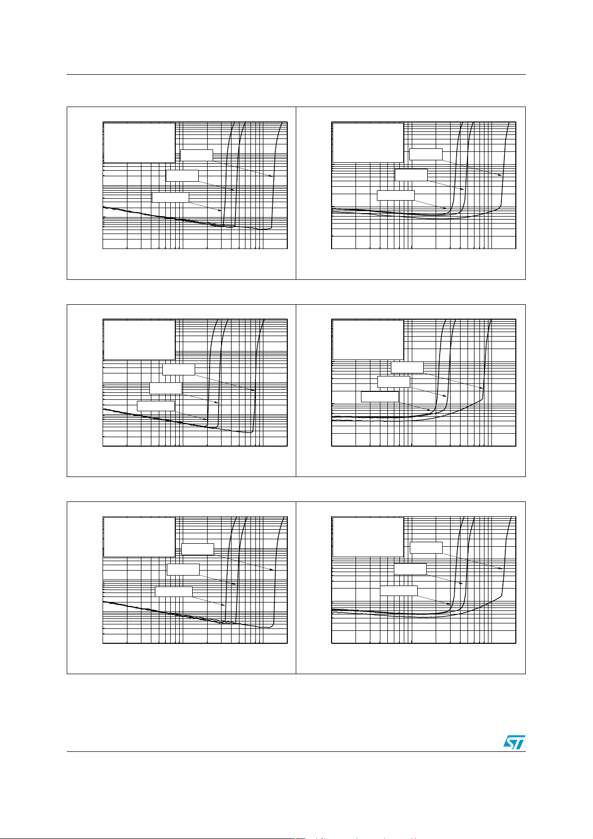
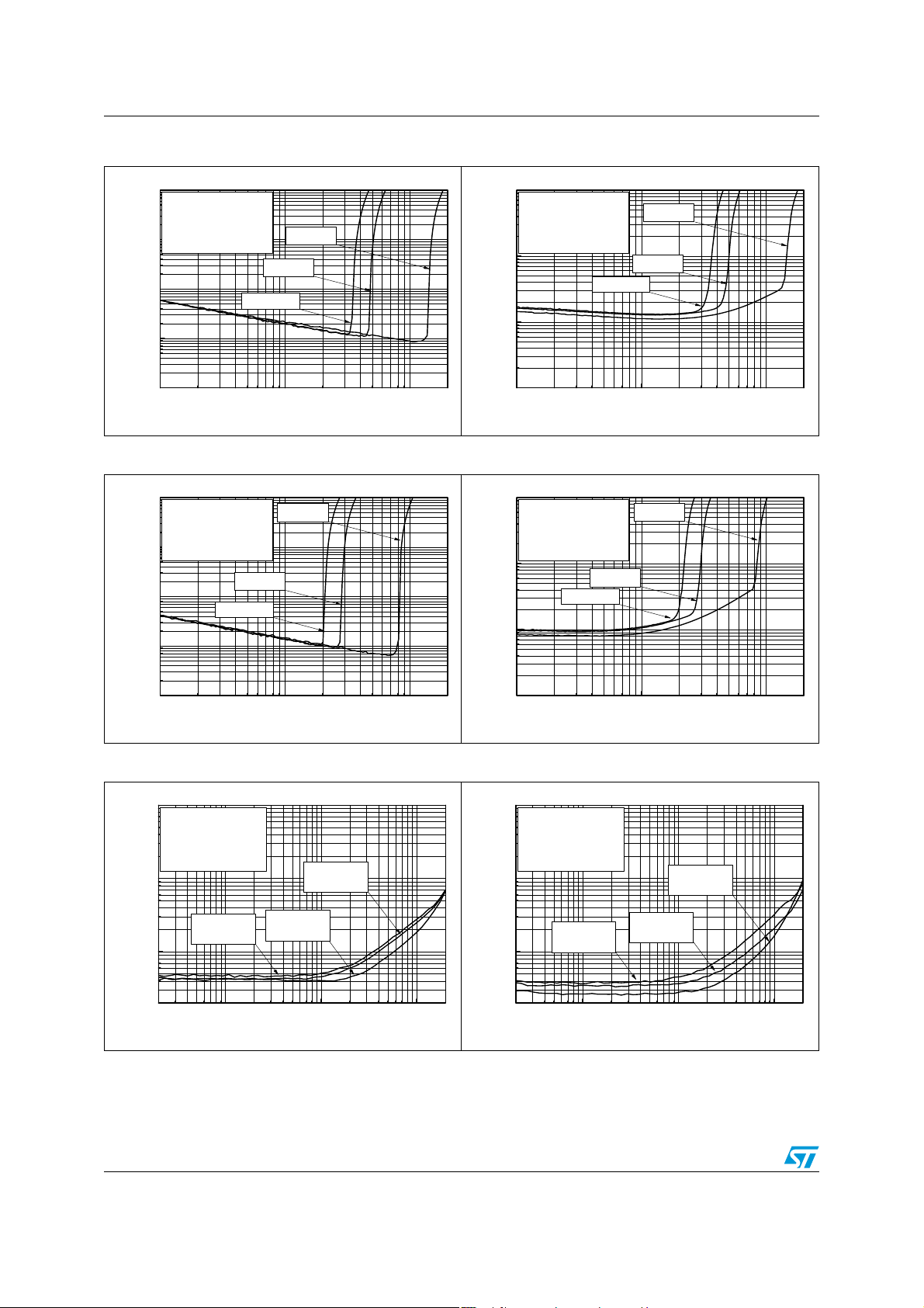
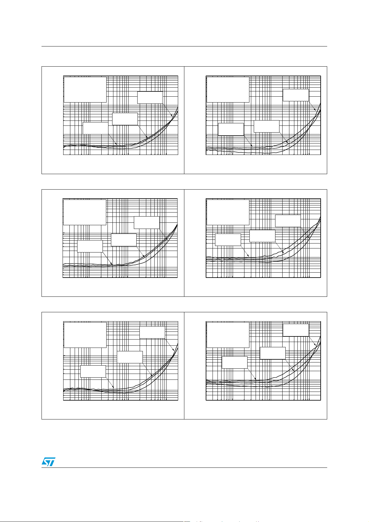
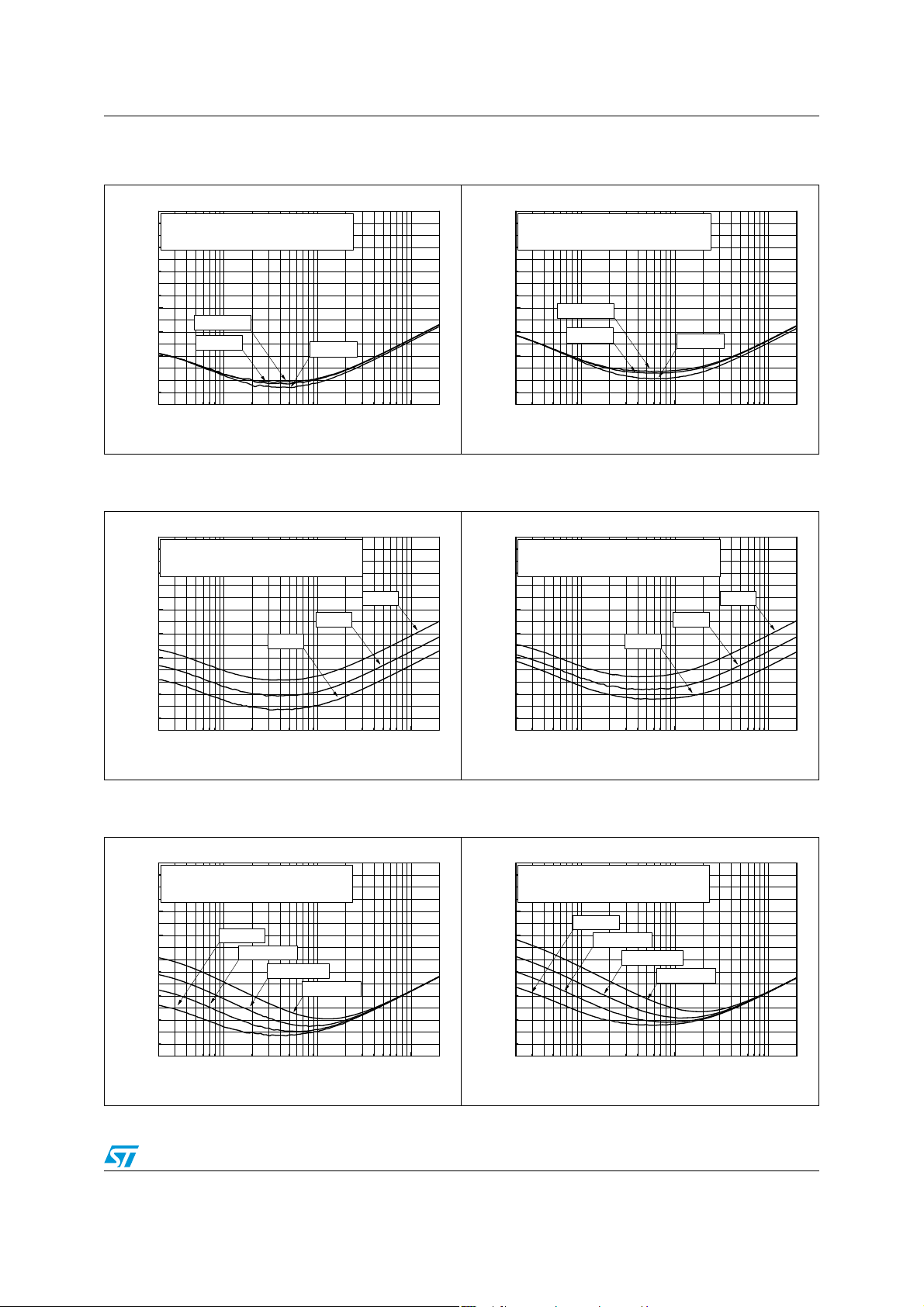
Table 7. Index of graphics
Description Figure
Open-loop frequency response Figure 2 to 6
Output swing vs. power supply voltage Figure 7
THD+N vs. output power Figure 8 to 23
THD+N vs. frequency Figure 24 to 31
Output power vs. power supply voltage Figure 32 to 35
Output power vs. load resistance Figure 36 to 41
Power dissipation vs. output power Figure 42 to 47
Crosstalk vs. frequency Figure 48 to 53
Signal to noise ratio vs. power supply voltage Figure 54 to 61
Pow er supply rejection ratio vs. frequency Figure 62 to 67
Current consumption vs. power supply voltage Figure 68 and 69
Current consumption vs. standby voltage Figure 70 to 75
Power derating curves Figure 76
8/32
TS4909 Electrical characteristics
Figure 2. Open-loop frequency response Figure 3. Open-loop frequency response
150
125
100
gain
phase
75
50
Gain (dB)
25
0
-25
-50
-1
10
RL=1MΩ, T
=25°C
AMB
10 10
3
5
10
Frequency (Hz)
90
45
0
-45
-90
Phase (°)
-135
-180
-225
-270
7
10
100
75
50
gain
25
0
Gain (dB)
-25
phase
-50
-75
RL=100Ω, CL=400pF, T
-100
-1
10
10 10
AMB
=25°C
3
5
10
10
Frequency (Hz)
Figure 4. Open-loop frequency response Figure 5. Open-loop frequency response
150
125
100
75
50
Gain (dB)
25
0
-25
RL=1MΩ, CL=100pF, T
-50
-1
10
gain
AMB
10 10
Frequency (Hz)
=25°C
3
10
phase
5
90
45
0
-45
-90
Phase (°)
-135
-180
-225
-270
7
10
100
75
50
gain
25
0
-25
phase
Gain (dB)
-50
-75
-100
-1
10
RL=16Ω, T
=25°C
AMB
10 10
3
5
10
10
Frequency (Hz)
90
45
0
-45
-90
-135
-180
-225
-270
7
90
45
0
-45
-90
-135
-180
-225
-270
7
Phase (°)
Phase (°)
Figure 6. Open-loop frequency response Figure 7. Output swing vs. power supply
voltage
100
75
50
25
0
Gain (dB)
-25
-50
-75
-100
-1
10
phase
RL=16Ω, CL=400pF, T
10 10
Frequency (Hz)
AMB
=25°C
3
90
45
gain
0
-45
-90
Phase (°)
-135
-180
-225
5
10
-270
7
10
6
T
=25°C
AMB
5
4
(V)
OL
3
& V
OH
V
2
RL=16
Ω
RL=32
Ω
1
0
23456
Power Supply Voltage (V)
9/32
Electrical characteristics TS4909
Figure 8. THD+N vs. output power Figure 9. THD+N vs. output power
10
Phantom Ground
F=1kHz, RL=16
Av=-1, Tamb=25°C
1
BW=20Hz-120kHz
Ω
Vcc=5V
Vcc=3V
0.1
THD+N (%)
Vcc=2.6V
0.01
1E-3
1E-3 0.01 0.1
Output Power (mW)
0.2
10
Phantom Ground
F=20kHz, RL=16
Av=-1, Tamb=25°C
BW=20Hz-120kHz
Ω
Vcc=5V
1
Vcc=3V
THD+N (%)
Vcc=2.6V
0.1
0.01
1E-3 0.01 0.1
Output Power (mW)
Figure 10. THD+N vs. output power Figure 11. THD+N vs. output power
THD+N (%)
0.01
10
Phantom Ground
F=1kHz, RL=32
Av=-1, Tamb=25°C
1
BW=20Hz-120kHz
0.1
Ω
Vcc=5V
Vcc=3V
Vcc=2.6V
THD+N (%)
10
Phantom Ground
F=20kHz, RL=32
Av=-1, Tamb=25°C
BW=20Hz-120kHz
1
0.1
Ω
Vcc=5V
Vcc=3V
Vcc=2.6V
0.2
1E-3
1E-3 0.01 0.1
Output Power (mW)
0.2
0.01
1E-3 0.01 0.1
Output Power (mW)
Figure 12. THD+N vs. output power Figure 13. THD+N vs. output power
10
Single Ended
F=1kHz, RL=16
Av=-1, Tamb=25°C
1
BW=20Hz-120kHz
Ω
Vcc=5V
Vcc=3V
0.1
THD+N (%)
Vcc=2.6V
0.01
1E-3
1E-3 0.01 0.1
Output Power (mW)
0.2
10
Single Ended
F=20kHz, RL=16
Av=-1, Tamb=25°C
BW=20Hz-120kHz
Ω
Vcc=5V
1
Vcc=3V
THD+N (%)
Vcc=2.6V
0.1
0.01
1E-3 0.01 0.1
Output Power (mW)
0.2
0.2
10/32

TS4909 Electrical characteristics
Figure 14. THD+N vs. output power Figure 15. THD+N vs. output power
10
Single Ended
F=1kHz, RL=32
Av=-1, Tamb=25°C
1
BW=20Hz-120kHz
Ω
Vcc=5V
0.1
THD+N (%)
0.01
1E-3
1E-3 0.01 0.1
Vcc=3V
Vcc=2.6V
Output Power (mW)
0.2
10
Single Ended
F=20kHz, RL=32
Ω
Av=-1, Tamb=25°C
BW=20Hz-120kHz
1
Vcc=5V
Vcc=3V
THD+N (%)
0.1
0.01
1E-3 0.01 0.1
Vcc=2.6V
Output Power (mW)
Figure 16. THD+N vs. output power Figure 17. THD+N vs. output power
THD+N (%)
0.01
10
Phantom Ground
F=1kHz, RL=16
Av=-4, Tamb=25°C
1
BW=20Hz-120kHz
0.1
Ω
Vcc=5V
Vcc=3V
Vcc=2.6V
THD+N (%)
10
Phantom Ground
F=20kHz, RL=16
Av=-4, Tamb=25°C
BW=20Hz-120kHz
1
0.1
Ω
Vcc=2.6V
Vcc=5V
Vcc=3V
0.2
1E-3
1E-3 0.01 0.1
Output Power (mW)
0.2
0.01
1E-3 0.01 0.1
Output Power (mW)
Figure 18. THD+N vs. output power Figure 19. THD+N vs. output power
10
Phantom Ground
F=1kHz, RL=32
Av=-4, Tamb=25°C
1
BW=20Hz-120kHz
Vcc=5V
Ω
Vcc=3V
0.1
THD+N (%)
Vcc=2.6V
0.01
1E-3
1E-3 0.01 0.1
Output Power (mW)
0.2
10
Phantom Ground
F=20kHz, RL=32
Vcc=5V
Ω
Av=-4, Tamb=25°C
BW=20Hz-120kHz
1
Vcc=3V
Vcc=2.6V
THD+N (%)
0.1
0.01
1E-3 0.01 0.1
Output Power (mW)
0.2
0.2
11/32
Electrical characteristics TS4909
Figure 20. THD+N vs. output power Figure 21. THD+N vs. output power
10
Single Ended
F=1kHz, RL=16
Av=-4, Tamb=25°C
1
BW=20Hz-120kHz
Ω
Vcc=5V
Vcc=3V
0.1
THD+N (%)
Vcc=2.6V
0.01
1E-3
1E-3 0.01 0.1
Output Power (mW)
0.2
10
Single Ended
F=20kHz, RL=16
Vcc=5V
Ω
Av=-4, Tamb=25°C
BW=20Hz-120kHz
1
Vcc=3V
Vcc=2.6V
THD+N (%)
0.1
0.01
1E-3 0.01 0.1
Output Power (mW)
Figure 22. THD+N vs. output power Figure 23. THD+N vs. output power
THD+N (%)
0.01
10
Single Ended
F=1kHz, RL=32
Av=-4, Tamb=25°C
1
BW=20Hz-120kHz
0.1
Ω
Vcc=3V
Vcc=2.6V
Vcc=5V
THD+N (%)
10
Single Ended
F=20kHz, RL=32
Av=-4, Tamb=25°C
BW=20Hz-120kHz
1
0.1
Vcc=3V
Vcc=2.6V
Vcc=5V
Ω
0.2
1E-3
1E-3 0.01 0.1
Output Power (mW)
0.2
0.01
1E-3 0.01 0.1
Output Power (mW)
Figure 24. THD+N vs. frequency Figure 25. THD+N vs. frequency
THD+N (%)
0.002
1
Phantom Ground
RL=16
BW=20Hz-120kHz
T
0.1
0.01
20
Ω,
Av=-1
=25°C
AMB
Vcc=3V
Po=40mW
Vcc=2.6V
Po=30mW
Vcc=5V
Po=90mW
100 1k 10k
Frequency (Hz)
20k
1
0.1
THD+N (%)
0.01
0.002
Phantom Ground
RL=32
Ω,
Av=-1
BW=20Hz-120kHz
T
=25°C
AMB
Vcc=2.6V
Po=20mW
20
100 1k 10k
Vcc=5V
Po=60mW
Vcc=3V
Po=25mW
Frequency (Hz)
0.2
20k
12/32
TS4909 Electrical characteristics
Figure 26. THD+N vs. frequency Figure 27. THD+N vs. frequency
THD+N (%)
0.002
1
Single Ended
RL=16Ω,Av=-1
BW=20Hz-120kHz
T
0.1
0.01
20
=25°C
AMB
Vcc=3V
Vcc=2.6V
Po=40mW
Po=30mW
100 1k 10k
Frequency (Hz)
Vcc=5V
Po=90mW
20k
1
0.1
THD+N (%)
0.01
0.002
Single Ended
RL=32
Ω,
Av=-1
BW=20Hz-120kHz
T
=25°C
AMB
Vcc=2.6V
Po=20mW
20
100 1k 10k
Vcc=3V
Po=25mW
Frequency (Hz)
Figure 28. THD+N vs. frequency Figure 29. THD+N vs. frequency
1
0.1
THD+N (%)
0.01
0.002
Phantom Ground
RL=32
Ω,
Av=-4
BW=20Hz-120kHz
T
=25°C
AMB
Vcc=2.6V
Po=20mW
20
100 1k 10k
Vcc=5V
Po=60mW
Vcc=3V
Po=25mW
Frequency (Hz)
THD+N (%)
0.01
0.005
1
0.1
20
Phantom Ground
RL=16
Ω,
Av=-4
BW=20Hz-120kHz
T
=25°C
AMB
Vcc=2.6V
Po=30mW
100 1k 10k
Vcc=5V
Po=90mW
Vcc=3V
Po=40mW
20k
Frequency (Hz)
Vcc=5V
Po=60mW
20k
20k
Figure 30. THD+N vs. frequency Figure 31. THD+N vs. frequency
1
Single Ended
RL=32
Ω,
Av=-4
BW=20Hz-120kHz
T
=25°C
AMB
0.1
Vcc=2.6V
THD+N (%)
Po=20mW
Vcc=3V
Po=25mW
0.01
0.002
20
100 1k 10k
Frequency (Hz)
13/32
THD+N (%)
0.005
1
Single Ended
RL=16
BW=20Hz-120kHz
T
0.1
0.01
20
Ω,
Av=-4
=25°C
AMB
Vcc=3V
Po=40mW
Vcc=2.6V
Po=30mW
100 1k 10k
Frequency (Hz)
Vcc=5V
Po=90mW
20k
Vcc=5V
Po=60mW
20k

Electrical characteristics TS4909
Figure 32. Output power vs. power supply
voltage
240
Phantom Ground
RL=16Ω, F=1kHz
200
Av=-1, T
BW=20Hz-120kHz
160
120
80
Output Power (mW)
40
0
23456
=25°C
AMB
THD+N=10%
THD+N=1%
Power Supply Voltage (V)
Figure 34. Output power vs. power supply
voltage
240
Single Ended
RL=16Ω, F=1kHz
200
Output Power (mW)
160
120
80
40
Av=-1, T
BW=20Hz-120kHz
AMB
=25°C
THD+N=10%
THD+N=1%
Figure 33. Output power vs. power supply
voltage
140
Phantom Ground
RL=32Ω, F=1kHz
120
Av=-1, T
BW=20Hz-12 0kH z
100
80
60
Output Power (mW)
40
20
0
23456
=25°C
AMB
Powe r S u p ply V o lt ag e (V )
THD+N=10%
THD+N=1%
Figure 35. Output power vs. power supply
voltage
140
Single Ended
RL=32Ω, F=1kHz
120
Output Power (mW)
100
80
60
40
20
Av=-1, T
BW=20Hz-12 0kH z
AMB
=25°C
THD+N=10%
THD+N=1%
0
23456
Power Supply Voltage (V)
0
23456
Powe r S u p ply V o lt ag e (V )
Figure 36. Output power vs. load resistance Figure 37. Output power vs. load resistance
50
40
30
20
Output Power (mW)
10
0
16 32 48 64 80 96
THD+N=10%
THD+N=1%
Load Resistance (Ω)
Phantom Ground
Vcc=2.6V, F=1kHz
Av=-1, T
BW=20Hz-12 0kH z
AMB
=25°C
14/32
50
40
30
20
Output Power (mW)
10
0
16 32 48 64 80 96
THD+N=10%
THD+N=1%
Load Resistance (Ω)
Single Ended
Vcc=2.6V, F=1kHz
Av=-1, T
AMB
BW=20Hz-120kHz
=25°C
TS4909 Electrical characteristics
Figure 38. Output power vs. load resistance Figure 39. Output power vs. load resistance
80
Phantom Ground
Vcc=3V, F=1kHz
Av=-1, T
60
40
Output Power (mW)
20
0
16 32 48 64 80 96
THD+N=10%
THD+N=1%
Load Resistance (Ω)
AMB
BW=20Hz-120kHz
=25°C
80
Single Ended
Vcc=3V, F=1kHz
Av=-1, T
60
40
Output Power (mW)
20
0
16 32 48 64 80 96
THD+N=10%
THD+N=1%
Load Resistance (Ω)
AMB
BW=20Hz-120kHz
=25°C
Figure 40. Output power vs. load resistance Figure 41. Output power vs. load resistance
200
150
100
THD+N=10%
THD+N=1%
Phantom Ground
Vcc=5V, F=1kHz
Av=-1, T
BW=20Hz-120kHz
AMB
=25°C
200
150
100
THD+N=10%
THD+N=1%
Single Ended
Vcc=5V, F=1kHz
Av=-1, T
BW=20Hz-120kHz
AMB
=25°C
Output Power (mW)
50
0
16 32 48 64 80 96
Load Resistance (Ω)
Output Power (mW)
50
0
16 32 48 64 80 96
Load Resistance (Ω)
Figure 42. Power dissipation vs. output power Figure 43. Power dissipation vs. output power
80
Phantom Ground
70
Vcc=2.6V, F=1kH z
THD+N<1%
60
50
RL=16
40
30
20
Power Dissipation (mW)
RL=32
Ω
10
0
0 5 10 15 20 25 30 35 40
Output Power (mW)
Ω
30
Single Ended
Vcc=2.6V, F=1kH z
25
THD+N<1%
RL=16Ω
20
15
RL=32Ω
10
Power Dissipation (mW)
5
0
0 5 10 15 20 25 30 35 40
Output Power (mW)
15/32

Electrical characteristics TS4909
Figure 44. Power dissipation vs. output power Figure 45. Power dissipation vs. output power
120
Phantom Ground
Vcc=3V, F=1kHz
100
THD+N<1%
80
RL=16
60
Ω
40
Power Dissipation (mW)
20
0
0 102030405060
RL=32
Ω
Output Power (mW )
40
Single Ended
35
Vcc=3V, F=1kH z
THD+N<1%
30
RL=16
25
20
RL=32
Ω
15
10
Power Dissipation (mW)
5
0
0 5 10 15 20 25 30 35 40 45 50 55
Output Power (mW)
Ω
Figure 46. Power dissipation vs. output power Figure 47. Power dissipation vs. output power
300
250
200
150
100
Power Dissipation (mW)
50
Phantom Ground
Vcc=5V, F=1kHz
THD+N<1%
RL=32
RL=16
Ω
Ω
100
Single Ended
Vcc=5V, F=1kHz, THD+N<1%
80
60
40
Power Dissipation (mW)
20
RL=32
RL=16
Ω
Ω
0
0 20 40 60 80 100 120 140 160
Output Power (mW)
0
0 20 40 60 80 100 120 140 160
Output Power (mW)
Figure 48. Crosstalk vs. frequency Figure 49. Crosstalk vs. frequency
Crosstalk (dB)
0
-20
-40
-60
-80
-100
-120
Single Ended
Vcc=5V, RL=16
Av=-1, Po=90mW
T
=25°C
AMB
OUT1 to OUT2
20
Ω
OUT2 to OUT1
100 1k 10k
Frequency (Hz)
20k
Crosstalk (dB)
0
-20
-40
-60
-80
-100
-120
Single Ended
Vcc=5V, RL=32Ω
Av=-1, Po=60mW
T
=25°C
AMB
20
100 1k 10k
OUT2 to OUT1
Frequency (Hz)
OUT1 to OUT2
20k
16/32

TS4909 Electrical characteristics
Figure 50. Crosstalk vs. frequency Figure 51. Crosstalk vs. frequency
Crosstalk (dB)
0
-20
-40
-60
-80
-100
-120
Single Ended
Vcc=5V, RL=16
Av=-4, Po=90mW
T
=25°C
AMB
20
Ω
OUT1 to OUT2
OUT2 to OUT1
100 1k 10k
Frequency (Hz)
20k
Crosstalk (dB)
0
-20
-40
-60
-80
-100
-120
Single Ended
Vcc=5V, RL=32Ω
Av=-4, Po=60mW
T
=25°C
AMB
OUT2 to OUT1
20
100 1k 10k
OUT1 to O UT2
Frequency (Hz)
Figure 52. Crosstalk vs. frequency Figure 53. Crosstalk vs. frequency
0
Phantom ground
Vcc=5V, Av=-1 ,
-20
T
AMB
-40
=25°C
RL=16Ω, Po=90mW
0
Phantom ground
Vcc=5V, Av=-4 ,
-20
T
AMB
-40
=25°C
RL=16Ω, Po=90mW
20k
-60
Crosstalk (dB)
-80
-100
-120
20
100 1k 10k
RL=32Ω, Po=60mW
Frequency (Hz)
Figure 54. Signal to noise ratio vs. power
supply voltage
104
Unweighted Filter (20Hz-20kHz)
Phantom Ground
102
Av=-1, T
Cb=1μF
100
THD+N<0.4%
98
96
Signal to Noise Ratio (dB)
94
92
23456
=25°C
AMB
RL=32
Power Supply Voltage (V)
RL=16
Ω
Ω
-60
Crosstalk (dB)
-80
RL=32Ω, Po=60mW
Frequency (Hz)
20k
-100
-120
20
100 1k 10k
Figure 55. Signal to noise ratio vs. power
supply voltage
106
Unweighted Filter (20Hz-20kHz)
Single Ended
104
Av=-1, T
Cb=1μF
102
THD+N<0.4%
100
98
Signal to Noise Ratio (dB)
96
94
23456
=25°C
AMB
Powe r S u p ply V o lt ag e (V )
RL=32
Ω
RL=16
20k
Ω
17/32

Electrical characteristics TS4909
Figure 56. Signal to noise ratio vs. power
supply voltage
108
Phantom Ground
A-weighted Filter
106
Av=-1, T
Cb=1μF
104
THD+N<0.4%
102
100
Signal to Noise Ratio (dB)
98
96
23456
=25°C
AMB
RL=16
Ω
RL=32
Ω
Power Supply Voltage (V)
Figure 58. Signal to noise ratio vs. power
supply voltage
98
Unweighted Filter (20Hz-20kH z)
96
Phantom Ground
94
92
90
88
Signal to Noise Ratio (dB)
86
Av=-4, T
Cb=1μF
THD+N<0.4%
AMB
=25°C
RL=32
RL=16
Ω
Ω
Figure 57. Signal to noise ratio vs. power
supply voltage
108
Single Ended
A-weighte d F ilte r
106
Av=-1, T
Cb=1μF
104
THD+N<0.4%
102
100
Signal to Noise Ratio (dB)
98
96
23456
=25°C
AMB
Powe r S u p ply V o lt ag e (V )
RL=32
RL=16
Ω
Ω
Figure 59. Signal to noise ratio vs. power
supply voltage
96
Unweighted Filter (20Hz-20kH z)
Phantom Ground
94
92
90
Signal to Noise Ratio (dB)
88
Av=-4, T
Cb=1μF
THD+N<0.4%
AMB
=25°C
RL=32
RL=16
Ω
Ω
84
23456
Power Supply Voltage (V)
Figure 60. Signal to noise ratio vs. power
supply voltage
100
Phantom Ground
A-weighted Filter
98
Av=-4, T
Cb=1μF
96
THD+N<0.4%
94
92
Signal to Noise Ratio (dB)
90
88
23456
18/32
=25°C
AMB
RL=32
Power Supply Voltage (V)
RL=16
Ω
Ω
86
23456
Power Supply Voltage (V)
Figure 61. Signal to noise ratio vs. power
supply voltage
100
Phantom Ground
A-weighte d F ilte r
98
Av=-4, T
Cb=1μF
96
THD+N<0.4%
94
92
Signal to Noise Ratio (dB)
90
88
23456
=25°C
AMB
RL=32
Powe r S u p ply V o lt ag e (V )
RL=16
Ω
Ω
TS4909 Electrical characteristics
Figure 62. Power supply rejection rat io vs.
frequency
0
Phantom Ground, Inputs grou nded
-10
Av=-1, RL≥16Ω, Cb=1μF, T
-20
-30
-40
PSRR (dB)
-50
-60
-70
-80
Vcc=2.6V
Vcc=3V
20
100 1k 10k
Frequency (Hz)
AMB
=25°C
Vcc=5V
Figure 64. Power supply rejection rat io vs.
frequency
0
Phantom Ground, Inputs grounded
-10
Vcc=3V, RL≥16Ω, Cb=1μF, T
-20
-30
-40
PSRR (dB)
-50
-60
-70
-80
20
Av=-1
100 1k 10k
Frequency (Hz)
AMB
=25°C
Av=-4
Av=-2
Figure 63. Power supply rejection ratio vs.
frequency
0
Single Ended, Inputs grounded
-10
20k
Av=-1, RL≥16Ω, Cb=1μF, T
-20
-30
-40
PSRR (dB)
-50
-60
-70
-80
20
Vcc=2.6V
Vcc=3V
100 1k 10k
Frequency (Hz)
AMB
=25°C
Vcc=5V
Figure 65. Power supply rejection ratio vs.
frequency
0
Single Ended, Inputs grounded
-10
20k
Vcc=3V, RL≥16Ω, Cb=1μF, T
-20
-30
-40
PSRR (dB)
-50
-60
-70
-80
20
Av=-1
100 1k 10k
Frequency (Hz)
AMB
=25°C
Av=-2
20k
Av=-4
20k
Figure 66. Power supply rejection rat io vs.
frequency
0
Phantom Ground, Inputs grounded
-10
Av=-1, RL≥16Ω, Vcc=3V, T
-20
-30
-40
PSRR (dB)
-50
-60
-70
-80
20
Cb=1μF
Cb=470nF
100 1k 10k
Frequency (Hz)
AMB
Cb=220nF
Cb=100nF
=25°C
Figure 67. Power supply rejection ratio vs.
frequency
0
Single Ended, Inputs grounded
-10
Av=-1, RL≥16Ω, Vcc=3V , T
20k
-20
-30
-40
PSRR (dB)
-50
-60
-70
-80
20
Cb=1μF
Cb=470nF
100 1k 10k
Frequency (Hz)
19/32
AMB
Cb=220nF
Cb=100nF
=25°C
20k

Electrical characteristics TS4909
Figure 68. Current consumption vs. power
supply voltage
4.0
3.5
3.0
2.5
2.0
T
1.5
T
1.0
Current Consumption (mA)
0.5
0.0
23456
T
=-40°C
AMB
Power Supply Voltage (V)
AMB
=25°C
=85°C
AMB
Phantom ground
No Loads
Figure 70. Current consumption vs. standby
voltage
4
T
=85°C
T
T
AMB
AMB
AMB
=25°C
=-40°C
3
2
Figure 69. Current consumption vs. power
supply voltage
3.0
2.5
2.0
1.5
1.0
T
=25°C
Current Consumption (mA)
0.5
0.0
23456
T
=-40°C
AMB
Power Supply Voltage (V)
AMB
T
=85°C
AMB
Single ended
No Loads
Figure 71. Current consumption vs. standby
voltage
2.5
T
=85°C
AMB
2.0
1.5
1.0
T
T
AMB
AMB
=25°C
=-40°C
1
Current Consumption (mA)
Phantom ground
VCC=2.6V
0
0.0 0.5 1.0 1.5 2.0 2.5
Standby Voltage (V)
Figure 72. Current consumption vs. standby
voltage
4
T
=85°C
AMB
3
2
1
Current Consumption (mA)
0
0.0 0.5 1.0 1.5 2.0 2.5 3.0
Standby Voltage (V)
T
=25°C
AMB
T
=-40°C
AMB
Phantom ground
VCC=3V
0.5
Current Consumption (mA)
Single ended
VCC=2.6V
0.0
0.0 0.5 1.0 1.5 2.0 2.5
Standby Vo ltage (V )
Figure 73. Current consumption vs. standby
voltage
2.5
2.0
1.5
1.0
0.5
Current Consumption (mA)
0.0
0.0 0.5 1.0 1.5 2.0 2.5 3.0
Standby Voltage (V)
T
=85°C
AMB
T
=25°C
AMB
T
=-40°C
AMB
Single ended
VCC=3V
20/32

TS4909 Electrical characteristics
Figure 74. Current consumption vs. standby
voltage
8
T
=85°C
AMB
6
T
=25°C
AMB
T
=-40°C
AMB
4
2
Current Consumption (mA)
Phantom ground
VCC=5V
0
0.0 0.5 1.0 1.5 2.0 4 5
Standby Voltage (V)
Figure 76. Power derating curves
3.5
3.0
2.5
Mounted on a 4-layer PCB
Figure 75. Current consumption vs. standby
voltage
8
T
6
4
2
Current Consumption (mA)
0
0.0 0.5 1.0 1.5 2.0 4 5
Standby Vo ltage (V )
AMB
=85°C
T
=25°C
AMB
T
AMB
Single ended
VCC=5V
=-40°C
2.0
No Heat sink
1.5
1.0
0.5
DFN10 Package Power Dissipation (W)
0.0
0 25 50 75 100 12 5 150
Ambiant Temperature
(
°
C
)
21/32

Application information TS4909
4 Application information
4.1 General description
The TS4909 integrates two monolithic power amplifiers. The amplifier output can be
configured to provide either single-ended (SE) capacitively-coupled output or phantom
ground (PHG) capacitor-less output. Fig ure 1: T ypical applications f or the TS4909 on page 3
shows schematics for each of these configurations.
Single-ended configuration
In the single-ended configuration, an output coupling capacitor, C
power amplifier (V
a DC voltage equal to V
out1
and V
out2
/2 and the output coupling capacitor blocks this reference v olta ge .
CC
Phantom ground configuration
In the phantom ground configuration, an internal buffer (V
and the output of the power amplifiers are also biased to the V
output coupling capacitors are needed. This is of primary importance in portable
applications where space constraints are continually present.
4.2 Frequency response
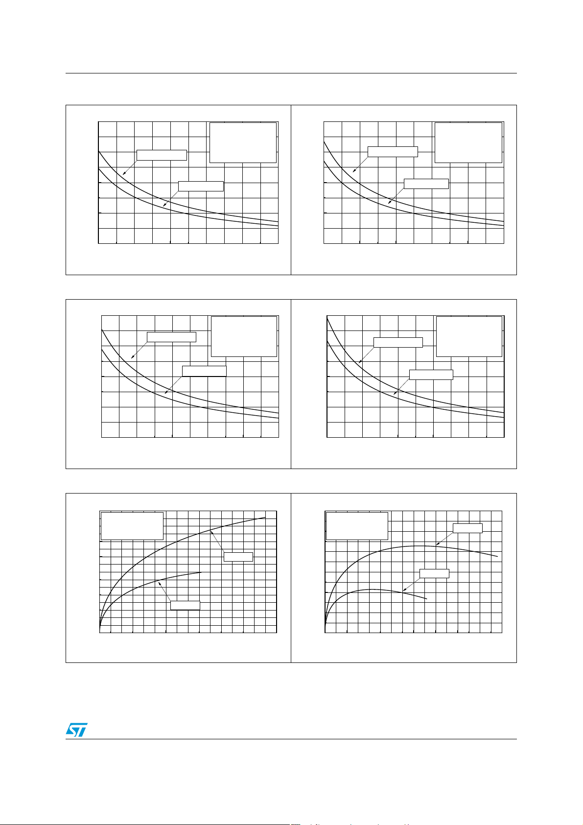
Higher cut-off frequency
In the high frequency region, you can limit the bandwidth by adding a capacitor C
parallel with R
that F
value of C
is the highest frequency to be amplified (with a 3dB att enuation), the maximum
CH
feed
Figure 77. Higher cut-off frequency vs. feedback capacitor
. It forms a low-pass filter with a -3dB cut-off frequency FCH. Assuming
feed
is:
, on the output of the
out
) is mandatory . The output of t he pow er amplifier is biased to
) maintains the VCC/2 voltage
out3
CH
--------------------------------------------------=
2π R
F
1
⋅⋅
feedCfeed
/2 voltage. Therefore, no
CC
feed
in
100k
10k
Rfeed=40k
1k
Higher Cut-off Frequency (kHz)
100
0.01 0.1 1 10 100
Rfeed=80k
22/32
Rfeed=10k
Ω
Ω
Cfeed
(
μ
F
)
Ω
Rfeed=20k
Ω
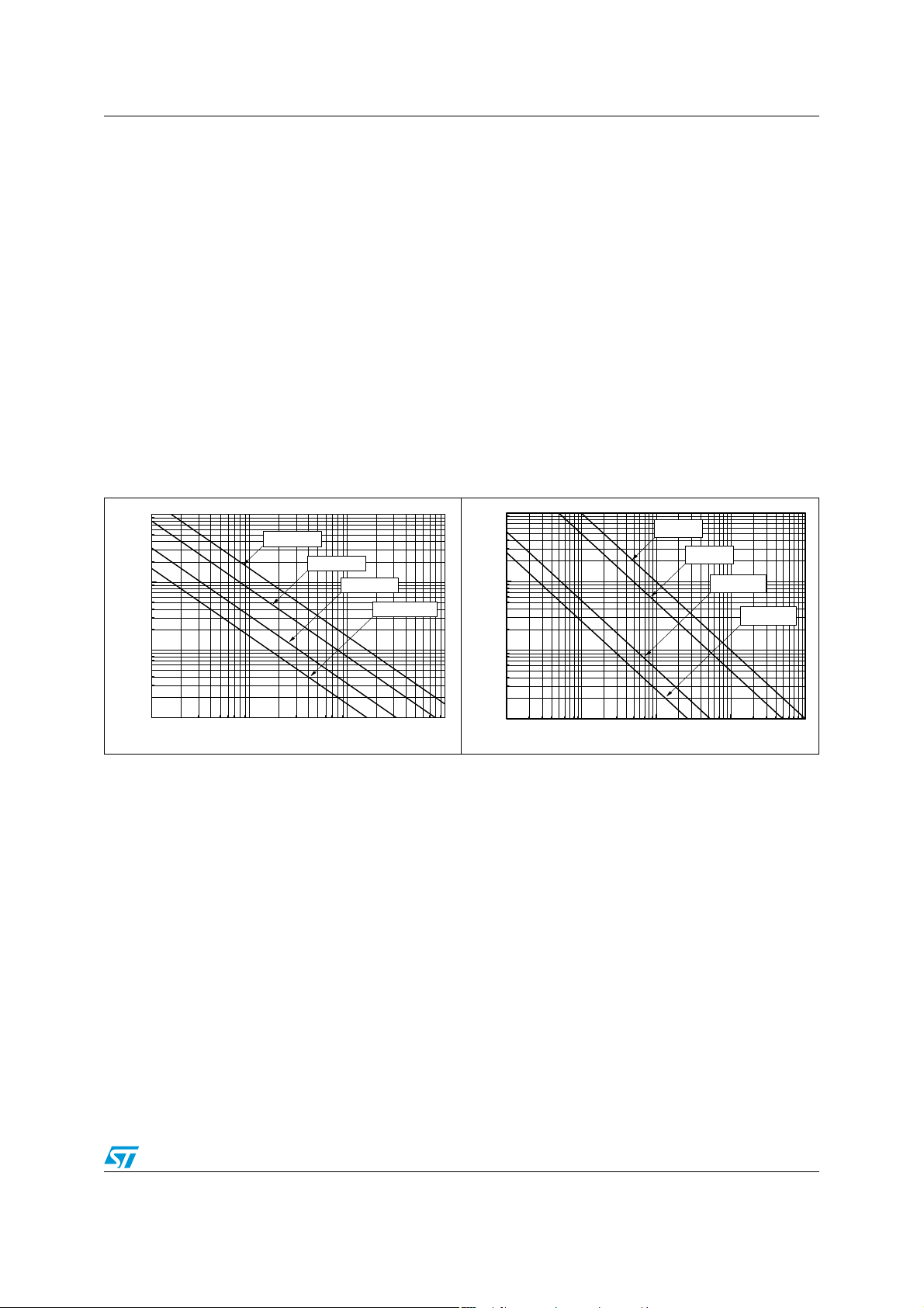
TS4909 Application information
0
Lower cut-off frequency
The lower cut-off frequency FCL of the TS4909 depends on input capacitor s C
single-ended configuration, F
The input capacitor C
in series with the input resistor Rin of the amplifier is equivalent to a
in
depends on output capacitors C
CL
first-order high-pass filter. Assuming that F
3dB attenuation), the minimum value of C
In the single-ended configuration, the capacitor C
equivalent to a first-order high-pass filter. Assuming that F
amplified (with a 3dB attenuation), the minimum value of C
C
Figure 78. Lower cut-off frequency vs. input
capacitor
10k
Rin=10k
Ω
Rin=20k
Ω
1k
Rin=50k
Ω
Rin=100k
Ω
. In the
in1,2
C
out
in
as well.
out1,2
is the lowest frequency to be amplified (with a
CL
is:
in
1
--------------------------------------- -=
⋅⋅
2π F
CLRin
in series with the load resistor RL is
1
--------------------------------------=
2π F
⋅⋅
CLRL
out
is the lowest frequency to be
CL
is:
out
Figure 79. Lower cut-off frequency vs. output
capacitor
10k
1k
RL=16
Ω
RL=32
Ω
RL=300
RL=600
Ω
Ω
100
Lower Cut-off frequency (Hz)
10
1 10 100 1000
Cin (nF)
100
Lower Cut-off frequency (Hz)
10
0.1 1 10 100 100
Cout
(
μ
F
)
Note: If FCL is kept the same for calculation purposes, it must be taken in account that the 1st-
order high-pass filter on the input and the 1st-order high-pass filter on the output create a
2nd-order high-pass filter in the audio signal path with an attenuation 6dB on F
off of 40db
⁄
decade.
and a roll-
CL
4.3 Gain using the typical application schematics
In the flat region (no Cin effect), the output voltage of a channel is:
R
feed
V
OUT
The gain A
is:
V
Note: The configuratio n (either single -ende d or phant om g round ) has n o effect on the value of the
gain.
⎛⎞
V
--------------–
⋅ VINAV⋅==
IN
⎝⎠
R
in
R
--------------–=
feed
R
in
A
V
23/32

Application information TS4909
4.4 Power dissipation and efficiency
Hypotheses:
● Voltage and current (V
● Supply voltage (V
CC
and I
out
) is a pure DC source.
Regarding the load we have:
and
and
4.4.1 Single-ended configuration
The aver age current delivered by the power supply voltage is:
Icc
AVG
Figure 80. Current delivered by power supply voltage in single-ended configuration
------
2π
π
1
∫
0
) in the load are sinusoidal.
out
V
OUTVPEAK
I
OUT
P
OUT
V
PEAK
-----------------
R
L
t()sin td
V
OUT
--------------
R
L
2
V
PEAK
-----------------
2R
ωtV()sin=
A()=
L
V
-----------------
A()=
PEAK
πR
L
A()==
Icc (t)
Vpeak/R
L
Icc
AVG
03T/22T
T/2 T
The power delivered by the power supply voltage is:
P
supply
VCCI
CC
AVG
W()=
Therefore, the power dissipation by each power amplifier is
P
dissPsupplyPOUT
2V
CC
diss
------------------ -
π R
P
P
OUTPOUT
L
W()–=
and the maximum value is obtained when:
∂P
diss
P
∂
0=
OUT
Time
W()–=
24/32

TS4909 Application information
and its value is:
2
V
CC
MAX
------------ -
π2R
W()=
L
P
diss
Note: This maximum value depends only on the power supply voltage and load values.
The efficiency is the ratio between the output power and the power supply:
η
P
OUT
-------------------
P
supply
πV
PEAK
-------------------- -==
2V
CC
The maximum theoretical value is reached when V
4.4.2 Phantom ground configuration
The aver age current delivered by the power supply voltage is:
π
1
Icc
AVG
Figure 81. Current delivered by power supply voltage in phantom ground
configuration
Icc (t)
Vpeak/R
L
Icc
AVG
03T/22T
The power delivered by the power supply voltage is:
-- -
∫
π
0
T/2 T
P
supply
η
V
PEAK
-----------------
R
π
-- - 78.5%==
4
L
VCCI
t()sin td
CC
AVG
PEAK
2V
-------------------- -
W()=
= VCC/2, so:
PEAK
A()==
πR
L
Time
Therefore, the power dissipation by each amplifier is
22V
CC
diss
----------------------
π R
L
P
OUTPOUT
W()–=
P
and the maximum value is obtained when:
∂P
diss
P
∂
0=
OUT
and its value is:
2
2V
CC
MAX
-------------- -
π2R
W()=
L
P
diss
Note: This maximum value depends only on power supply voltage and load values.
25/32

Application information TS4909
The efficiency is the ratio between the output power and the power supply:
η
P
OUT
-------------------
P
supply
πV
PEAK
-------------------- -==
4V
CC
The maximum theoretical value is reached when V
4.4.3 Total power dissipation
The TS4909 is a stereo (dual channel) amplifier. It has two independent power amplifiers.
Each amplifier produces heat due to its power dissipation. Therefore the maximum die
temperature is the sum of each amplifier’s maximum power dissipation. It is calculated as
follows:
● P
● P
● Total P
In most cases, P
Single-ended configuration:
Phantom ground configuration:
= power dissipation due to the first channel power amplifier (V
diss 1
= power dissipation due to the second channel power amplifier (V
diss 2
diss=Pdiss 1+Pdiss 2
= P
diss 1
diss 2
TotalP
TotalP
(W)
, giving:
TotalP
diss
diss
π
η
-- - 39.25%==
8
2P
==
diss
22V
CC
----------------------
π R
L
42V
CC
----------------------
π R
L
diss1
P
P
PEAK
OUT
OUT
2P
–=
–=
= VCC/2, so:
diss2
2P
OUT
2P
OUT
out1
).
out2
).
4.5 Decoupling of the circuit
Two capacitors are needed to properly bypass the TS4909 — a power supply capacitor Cs
and a bias voltage bypass capacit or C
C
has a strong influence on the THD+N at high frequencies (abo ve 7kHz) and indirectly on
s
the power supply disturbances. With 1 μF, you could expect the THD+N performance to be
similar to the values shown in this datasheet. If C
high frequencies and disturbances on the p ower supply r ail are less filtered. O n the contrary,
if C
is higher than 1 μF, those disturbances on the power supply rail are more filtered.
s
C
has an influence on THD+N at lower frequen cies, bu t its value is critical on the final result
b
of PSRR with inputs grounded in lower frequencies:
● If C
is lower than 1 μF, THD+N incr eases at lo wer f requencies and t he PSRR worsens
b
(increases).
● If C
is higher than 1 μF, the benefit on THD+N and PSRR in the low er frequen cy range
b
is small.
26/32
b
.
is lower than 1 μF, THD+N increases at
s

TS4909 Application information
4.6 Wake-up time
When the standby is released to turn the device ON, the bypass capacitor Cb is charged
immediately. As C
properly until the C
40ms (pop precaution) is called the wake-up time or t
characteristics tables with C
If C
has a value other than 1µF, you can calculate t
b
read it directly from the graph in Figure82.
● Single-ended configuration
● Phantom ground configuration
Figure 82. Typical wake-up time vs. bypass capacitance
is directly linked to the bias of the amplifier, the bias will not work
b
voltage is correct. The time to reach this voltage plus a time delay of
b
=1µF (see Section 3: Electrical characteristics on page 5).
b
Cb 2.5⋅
t
----------------------- 40 [ms;μF]+=
350
300
250
WU
t
WU
T
AMB
=25°C
0.042
Cb 2.5⋅
----------------------- 40 [ms;μF]+=
0.417
Single Ended
. It is specified in the electrical
WU
by using the following formulas, or
WU
Wake-up Time (ms)
Note: It is assumed the C
voltage is equal to 0 V. If the Cb voltage is not equal 0 V, the wake-up
b
time is lower.
4.7 Pop performance
Pop performance in the phantom ground configuration is closely linked with the size of the
input capacitor C
values requested.
In order to reach low pop, C
rule, the equivalent input constant time (R
τ
in
By following the pre vious rules , the TS4909 ca n reach low pop e ven with a high gain such as
20dB.
. The size of Cin is dependent on the lower cut-off frequency and PSRR
in
= RinxCin<0.008s
200
150
100
50
0
012345
must be charged to VCC/2 in less than 40ms. To follow this
in
inCin
Phantom Ground
Cb
(
μ
F
)
) should be less then 8ms:
27/32
Application information TS4909
Example calculation:
With Rin=20kΩ and FCL= 20Hz, -3db low cut-off frequency, Cin= 398nF. So, Cin= 390nF
with standard value which gives a lower cut-off frequency equal to 20.4Hz.
In this case,
τ
= RinxCin=7.8ms
in
This value is sufficient with regards to the previous f ormula, so we can state that the pop will
be imperceptible.
Connecting the headphones
Generally headphones are connected using a jack connector. To prevent pop in the
headphones while plugging in the jack, a pulldown resistor should be connected in parallel
with each headphone output. This allows the capacitors C
to be charged even when no
out
headphones are plugged in.
A resistor of 1 kΩ is high enough to be a negligible load, and low enough to charge the
capacitors C
in less than one second.
out
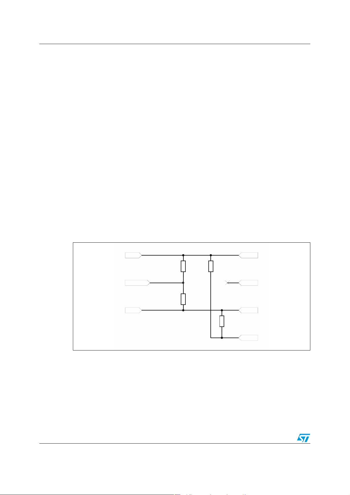
4.8 Standby mode
When the TS4909 is in standby mode, the time required to put the output stages (V
V
out2
and V
) into a high impedance state with reference to ground, and the internal
out3
out1
circuitry in standby mode, is a few microseconds.
Figure 83. Internal equivalent circuit schematics of the TS4909 in standby mode
Vin1
BYPASS
Vin2
25K
25K
1M
Vout1
Vout3
Vout2
1M
GND
,
28/32
TS4909 Package information
5 Package information
In order to meet environmental requirements, STMicroelectronics offers these devices in
ECOPACK
category of second level interconnect is marke d on the pa ckage and on the inner box label,
in compliance with JEDEC Standard JESD97. The maximum ratings related t o soldering
conditions are also marked on the inner box label. ECOPACK is an STMicroelectronics
trademark. ECOPACK specifications are available at: www.st.com
Figure 84. TS4909 footprint recommendation
®
packages. These packages have a lead-free second level interconnect. The
.
29/32
Package information TS4909
Figure 85. DFN10 3x3 exposed pad package mechanical data
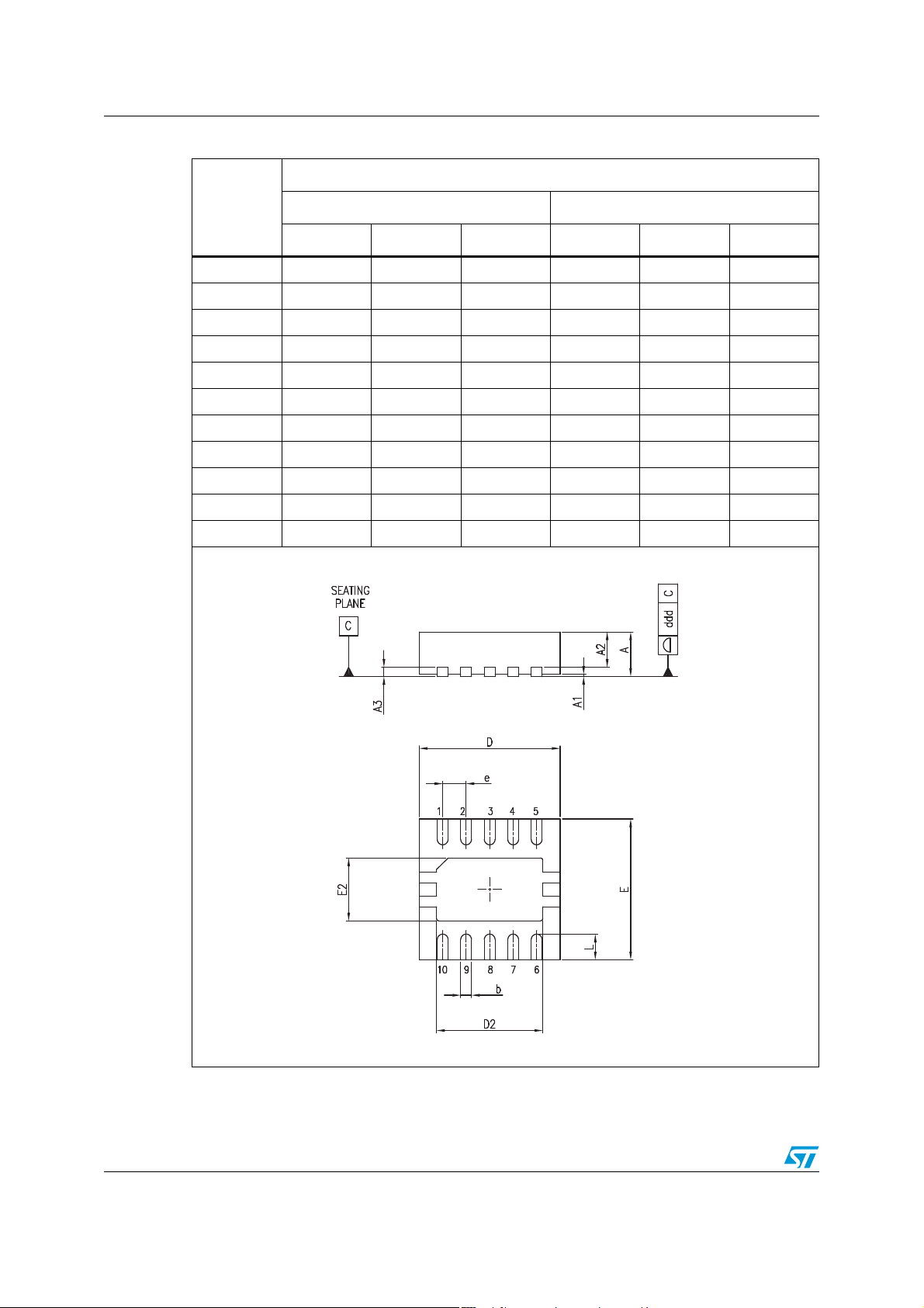
Dimensions
Ref.
Min. Typ. Max. Min. Typ. Max.
A 0.80 0.90 1.00 31.5 35.4 39.4
A1 0.02 0.05 0.8 2.0
A2 0.70 25.6
A3 0.20 7.9
b 0.18 0.23 0.30 7.1 9.1 11.8
D 3.00 118.1
D2 2.21 2.26 2.31 87.0 89.0 91.0
E 3.00 118.1
E2 1.49 1.64 1.74 58.7 64.6 68.5
e 0.50 19.7
L 0.3 0.4 0.5 11.8 15.7 19.7
Millimeters Mils
30/32
TS4909 Ordering information
6 Ordering information
Table 8. Order code
Part number Temperature range Package Packing Marking
TS4909IQT -40 °C to +85°C DFN1 0 Tape & reel K909
7 Revision history
Table 9. Document revision history
Date Revision Changes
1-Dec-2006 6 Release to production of the device.
2-Jan-2007 7
26-Sep-2007 8 Updated Table2: Absolute maximum ratings.
Correction of revision number of December revision (revision 6
instead of revision 5).
31/32

TS4909
Please Read Carefully:
Information in this document is provided solely in connection with ST products. STMicroelectronics NV and its subsidiaries (“ST”) reserve the
right to make changes, corrections, modifications or improvements, to this document, and the products and services described herein at any
time, without notice.
All ST products are sold pursuant to ST’s terms and conditions of sale.
Purchasers are solely res ponsibl e fo r the c hoic e, se lecti on an d use o f the S T prod ucts and s ervi ces d escr ibed he rein , and ST as sumes no
liability whatsoever relati ng to the choice, selection or use of the ST products and services described herein.
No license, express or implied, by estoppel or otherwise, to any intellectual property rights is granted under this document. If any part of this
document refers to any third pa rty p ro duc ts or se rv ices it sh all n ot be deem ed a lice ns e gr ant by ST fo r t he use of su ch thi r d party products
or services, or any intellectua l property c ontained the rein or consi dered as a warr anty coverin g the use in any manner whats oever of suc h
third party products or servi ces or any intellectual propert y contained therein.
UNLESS OTHERWISE SET FORTH IN ST’S TERMS AND CONDITIONS OF SALE ST DISCLAIMS ANY EXPRESS OR IMPLIED
WARRANTY WITH RESPECT TO THE USE AND/OR SALE OF ST PRODUCTS INCLUDING WITHOUT LIMITATION IMPLIED
WARRANTIES OF MERCHANTABILITY, FITNESS FOR A PARTICUL AR PURPOS E (AND THEIR EQUIVALE NTS UNDER THE LAWS
OF ANY JURISDICTION), OR INFRINGEMENT OF ANY PATENT, COPYRIGHT OR OTHER INTELLECTUAL PROPERTY RIGHT.
UNLESS EXPRESSLY APPROVED IN WRITING BY AN AUTHORIZED ST REPRESENTATIVE, ST PRODUCTS ARE NOT
RECOMMENDED, AUTHORIZED OR WARRANTED FOR USE IN MILITARY, AIR CRAFT, SPACE, LIFE SAVING, OR LIFE SUSTAINING
APPLICATIONS, NOR IN PRODUCTS OR SYSTEMS WHERE FAILURE OR MALFUNCTION MAY RESULT IN PERSONAL INJ URY,
DEATH, OR SEVERE PROPERTY OR ENVIRONMENTAL DAMAGE. ST PRODUCTS WHICH ARE NOT SPECIFIED AS "AUTOMOTIVE
GRADE" MAY ONLY BE USED IN AUTOMOTIVE APPLICATIONS AT USER’S OWN RISK.
Resale of ST products with provisions different from the statements and/or technical features set forth in this document shall immediately void
any warranty granted by ST fo r the ST pro duct or serv ice describe d herein and shall not cr eate or exten d in any manne r whatsoever , any
liability of ST.
ST and the ST logo are trademarks or registered trademarks of ST in vari ous countries.
Information in this document su persedes and replaces all information previously supplied.
The ST logo is a registered trademark of STMicroelectronics. All other names are the property of their respective owners.
© 2007 STMicroelectronics - All rights reserved
STMicroelectronics group of compan ie s
Australia - Belgium - Brazil - Canada - China - Czech Republic - Finland - Fran ce - Germany - Hong Kong - India - Israel - Italy - Japan -
Malaysia - Malta - Morocco - Singapore - Spain - Sweden - Switzerland - United Kingdom - United States of America
www.st.com
32/32
 Loading...