

Features
■ Input multiplexer
– QD1: quasi-differential stereo inputs
– SE1: stereo single-ended input
– SE2: stereo single-ended input
– SE3: stereo single-ended input
– FD1 / SE4+SE5: 1 full-differential input or 2
stereo single-ended inputs
■ Loudness
■ Volume
■ Bass
■ Middle
■ Treble
nd
–2
order frequency response
– Programmable center frequency
(400 Hz / 800 Hz / 2400 Hz)
– 15dB with 1dB steps
– Selectable high frequency boost
– Selectable flat-mode (constant attenuation)
– +23 dB to -31 dB with 1 dB step resolution
– Soft-step control with programmable blend
times
nd
–2
order frequency response
– Center frequency programmable in 4 steps
(60 Hz / 80 Hz / 100 Hz / 200 Hz)
– Q programmable 1.0/1.25/1.5/2.0
– DC gain programmable
– -15 dB to 15 dB range with 1 dB resolution
nd
–2
order frequency response
– Center frequency programmable in 4 steps
(500 Hz / 1 kHz / 1.5 kHz / 2.5 kHz)
– Q programmable 0.75/1.0/1.25
– -15 dB to 15 dB range with 1 dB resolution
nd
–2
order frequency response
(10 kHz / 12.5 kHz / 15 kHz / 17.5 kHz)
– Center frequency programmable in 4 steps
(10 kHz / 12.5 kHz / 15 kHz / 17.5 kHz)
– -15 dB to 15 dB with 1 dB resolution
TDA7718N
3 band car audio processor
TSSOP28
■ Speaker
– 4 independent soft step speaker controls
– +15 dB to -79 dB with 1 dB steps
– Direct mute
■ Subwoofer
■ Mute functions
■ Offset detection
Description
The TDA7718N is a high performance signal
processor specifically designed for car radio
applications. The device includes a high
performance audioprocessor with fully integrated
audio filters and new Soft Step architecture. The
digital control allows programming in a wide range
of filter characteristics.
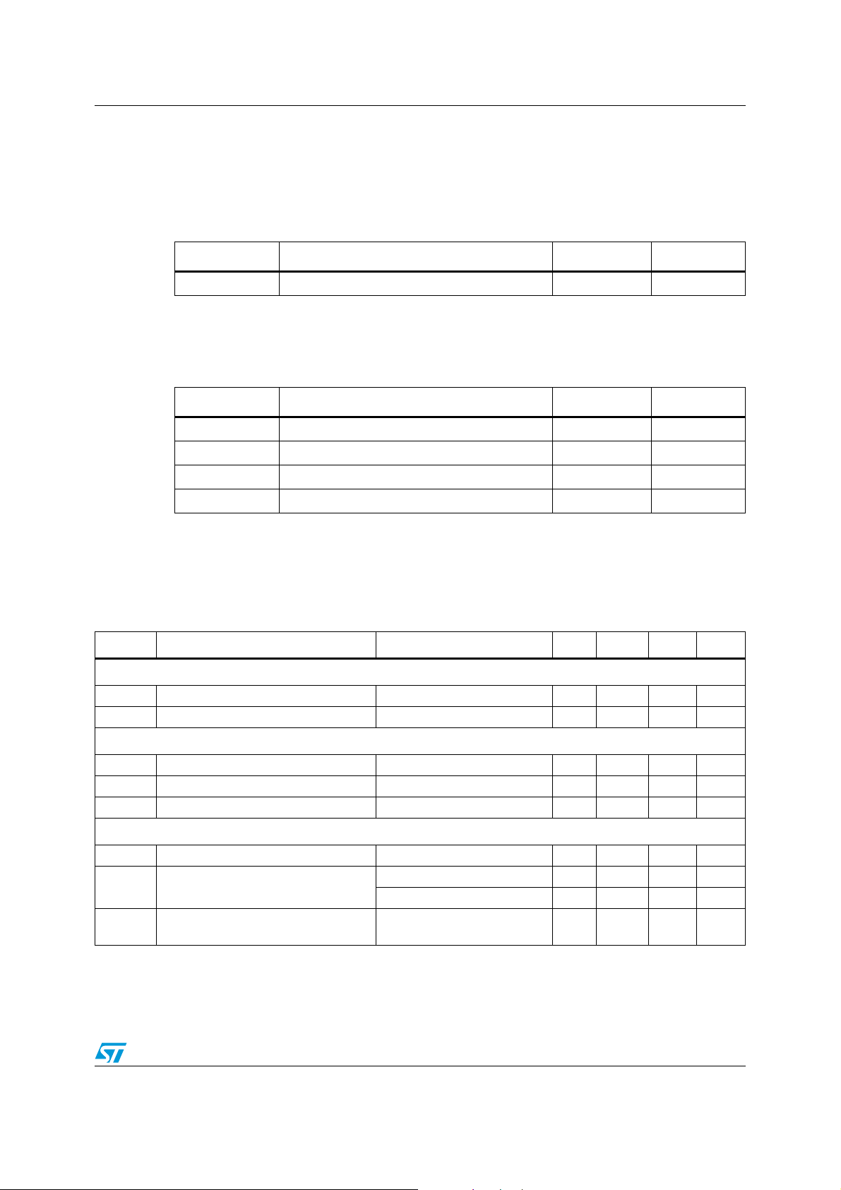
Table 1. Device summary
nd
–2
order low pass filter with programmable
cut off frequency
(55 Hz / 85 Hz / 120 Hz / 160 Hz)
– 2 independent soft step level control,
+15 dB to –79 dB with 1 dB steps
– Direct mute
– Digitally controlled SoftMute with 4
programmable mute-times
(0.48 ms/0.96 ms/8 ms/16 ms)
– Offset voltage detection circuit for on-board
power amplifier failure diagnosis
Order code Package Packing
TDA7718N TSSOP28 Tube
TDA7718NTR TSSOP28 Tape and reel
October 2009 Doc ID 16502 Rev 1 1/40
www.st.com
1

Contents TDA7718N
Contents
1 Block circuit diagram . . . . . . . . . . . . . . . . . . . . . . . . . . . . . . . . . . . . . . . . 6
2 Pin connection and pin description . . . . . . . . . . . . . . . . . . . . . . . . . . . . 7
2.1 Pin connection . . . . . . . . . . . . . . . . . . . . . . . . . . . . . . . . . . . . . . . . . . . . . . 7
2.2 Pin description . . . . . . . . . . . . . . . . . . . . . . . . . . . . . . . . . . . . . . . . . . . . . . 7
3 Electrical specifications . . . . . . . . . . . . . . . . . . . . . . . . . . . . . . . . . . . . . . 9
3.1 Thermal data . . . . . . . . . . . . . . . . . . . . . . . . . . . . . . . . . . . . . . . . . . . . . . . 9
3.2 Absolute maximum ratings . . . . . . . . . . . . . . . . . . . . . . . . . . . . . . . . . . . . . 9
3.3 Electrical characteristics . . . . . . . . . . . . . . . . . . . . . . . . . . . . . . . . . . . . . . . 9
4 Description of the audioprocessor . . . . . . . . . . . . . . . . . . . . . . . . . . . . 13
4.1 Input stages . . . . . . . . . . . . . . . . . . . . . . . . . . . . . . . . . . . . . . . . . . . . . . . 13
4.1.1 Quasi-differential stereo input (QD1) . . . . . . . . . . . . . . . . . . . . . . . . . . . 13
4.1.2 Single-ended stereo input (SE1, SE2, SE3) . . . . . . . . . . . . . . . . . . . . . 13
4.1.3
Full-differential stereo input or single-ended input (FD1/QD2/SE4+SE5)
13
4.2 Loudness . . . . . . . . . . . . . . . . . . . . . . . . . . . . . . . . . . . . . . . . . . . . . . . . . 15
4.2.1 Loudness attenuation . . . . . . . . . . . . . . . . . . . . . . . . . . . . . . . . . . . . . . 15
4.2.2 Peak frequency . . . . . . . . . . . . . . . . . . . . . . . . . . . . . . . . . . . . . . . . . . . 15
4.2.3 High frequency boost . . . . . . . . . . . . . . . . . . . . . . . . . . . . . . . . . . . . . . . 16
4.2.4 Flat mode . . . . . . . . . . . . . . . . . . . . . . . . . . . . . . . . . . . . . . . . . . . . . . . . 16
4.3 SoftMute . . . . . . . . . . . . . . . . . . . . . . . . . . . . . . . . . . . . . . . . . . . . . . . . . . 17
4.4 SoftStep volume . . . . . . . . . . . . . . . . . . . . . . . . . . . . . . . . . . . . . . . . . . . . 17
4.5 Bass . . . . . . . . . . . . . . . . . . . . . . . . . . . . . . . . . . . . . . . . . . . . . . . . . . . . . 18
4.5.1 Bass attenuation . . . . . . . . . . . . . . . . . . . . . . . . . . . . . . . . . . . . . . . . . . 18
4.5.2 Bass center frequency . . . . . . . . . . . . . . . . . . . . . . . . . . . . . . . . . . . . . . 18
4.5.3 Quality factors . . . . . . . . . . . . . . . . . . . . . . . . . . . . . . . . . . . . . . . . . . . . 19
4.5.4 DC mode . . . . . . . . . . . . . . . . . . . . . . . . . . . . . . . . . . . . . . . . . . . . . . . . 19
4.6 Middle . . . . . . . . . . . . . . . . . . . . . . . . . . . . . . . . . . . . . . . . . . . . . . . . . . . . 20
4.6.1 Middle attenuation . . . . . . . . . . . . . . . . . . . . . . . . . . . . . . . . . . . . . . . . . 20
4.6.2 Middle center frequency . . . . . . . . . . . . . . . . . . . . . . . . . . . . . . . . . . . . 20
4.6.3 Quality factors . . . . . . . . . . . . . . . . . . . . . . . . . . . . . . . . . . . . . . . . . . . . 21
4.7 Treble . . . . . . . . . . . . . . . . . . . . . . . . . . . . . . . . . . . . . . . . . . . . . . . . . . . . 21
2/40 Doc ID 16502 Rev 1

TDA7718N Contents
4.7.1 Treble attenuation . . . . . . . . . . . . . . . . . . . . . . . . . . . . . . . . . . . . . . . . . 21
4.7.2 Center frequency . . . . . . . . . . . . . . . . . . . . . . . . . . . . . . . . . . . . . . . . . . 22
4.8 Subwoofer filter . . . . . . . . . . . . . . . . . . . . . . . . . . . . . . . . . . . . . . . . . . . . 22
4.9 Softstep control . . . . . . . . . . . . . . . . . . . . . . . . . . . . . . . . . . . . . . . . . . . . 23
4.10 DC offset detector . . . . . . . . . . . . . . . . . . . . . . . . . . . . . . . . . . . . . . . . . . 23
4.11 Audioprocessor testing . . . . . . . . . . . . . . . . . . . . . . . . . . . . . . . . . . . . . . . 25
5I
2
C bus specification . . . . . . . . . . . . . . . . . . . . . . . . . . . . . . . . . . . . . . . . 26
5.1 Interface protocol . . . . . . . . . . . . . . . . . . . . . . . . . . . . . . . . . . . . . . . . . . . 26
5.2 I
2
C bus electrical characteristics . . . . . . . . . . . . . . . . . . . . . . . . . . . . . . . 26
5.2.1 Receive mode . . . . . . . . . . . . . . . . . . . . . . . . . . . . . . . . . . . . . . . . . . . . 27
5.2.2 Transmission mode . . . . . . . . . . . . . . . . . . . . . . . . . . . . . . . . . . . . . . . . 27
5.2.3 Reset condition . . . . . . . . . . . . . . . . . . . . . . . . . . . . . . . . . . . . . . . . . . . 27
5.3 Data byte specification . . . . . . . . . . . . . . . . . . . . . . . . . . . . . . . . . . . . . . . 29
6 Package information . . . . . . . . . . . . . . . . . . . . . . . . . . . . . . . . . . . . . . . . 38
7 Revision history . . . . . . . . . . . . . . . . . . . . . . . . . . . . . . . . . . . . . . . . . . . 39
Doc ID 16502 Rev 1 3/40

List of tables TDA7718N
List of tables
Table 1. Device summary . . . . . . . . . . . . . . . . . . . . . . . . . . . . . . . . . . . . . . . . . . . . . . . . . . . . . . . . . . 1
Table 2. Pin description . . . . . . . . . . . . . . . . . . . . . . . . . . . . . . . . . . . . . . . . . . . . . . . . . . . . . . . . . . . 7
Table 3. Thermal data. . . . . . . . . . . . . . . . . . . . . . . . . . . . . . . . . . . . . . . . . . . . . . . . . . . . . . . . . . . . . 9
Table 4. Absolute maximum ratings . . . . . . . . . . . . . . . . . . . . . . . . . . . . . . . . . . . . . . . . . . . . . . . . . . 9
Table 5. Electrical characteristics . . . . . . . . . . . . . . . . . . . . . . . . . . . . . . . . . . . . . . . . . . . . . . . . . . . . 9
Table 6. I
Table 7. Subaddress (receive mode) . . . . . . . . . . . . . . . . . . . . . . . . . . . . . . . . . . . . . . . . . . . . . . . . 28
Table 8. Main selector (0) . . . . . . . . . . . . . . . . . . . . . . . . . . . . . . . . . . . . . . . . . . . . . . . . . . . . . . . . . 29
Table 9. Soft mute / others (4) . . . . . . . . . . . . . . . . . . . . . . . . . . . . . . . . . . . . . . . . . . . . . . . . . . . . . 30
Table 10. SoftStep I (5). . . . . . . . . . . . . . . . . . . . . . . . . . . . . . . . . . . . . . . . . . . . . . . . . . . . . . . . . . . . 31
Table 11. SoftStep II / DC detector (6) . . . . . . . . . . . . . . . . . . . . . . . . . . . . . . . . . . . . . . . . . . . . . . . . 32
Table 12. Loudness (7) . . . . . . . . . . . . . . . . . . . . . . . . . . . . . . . . . . . . . . . . . . . . . . . . . . . . . . . . . . . . 33
Table 13. Volume / output gain (8) . . . . . . . . . . . . . . . . . . . . . . . . . . . . . . . . . . . . . . . . . . . . . . . . . . . 33
Table 14. Treble filter (9) . . . . . . . . . . . . . . . . . . . . . . . . . . . . . . . . . . . . . . . . . . . . . . . . . . . . . . . . . . 34
Table 15. Middle filter (10) . . . . . . . . . . . . . . . . . . . . . . . . . . . . . . . . . . . . . . . . . . . . . . . . . . . . . . . . . 34
Table 16. Bass filter (11). . . . . . . . . . . . . . . . . . . . . . . . . . . . . . . . . . . . . . . . . . . . . . . . . . . . . . . . . . . 35
Table 17. Subwoofer / middle / bass (12) . . . . . . . . . . . . . . . . . . . . . . . . . . . . . . . . . . . . . . . . . . . . . . 35
Table 18. Speaker attenuation (FL/FR/RL/RR/SWL/SWR) (13-18) . . . . . . . . . . . . . . . . . . . . . . . . . . 36
Table 19. Testing audio processor 1 (19) . . . . . . . . . . . . . . . . . . . . . . . . . . . . . . . . . . . . . . . . . . . . . . 36
Table 20. Testing audio processor 2 (20) . . . . . . . . . . . . . . . . . . . . . . . . . . . . . . . . . . . . . . . . . . . . . . 37
Table 21. Testing audio processor 3 (21) . . . . . . . . . . . . . . . . . . . . . . . . . . . . . . . . . . . . . . . . . . . . . . 37
Table 22. Document revision history . . . . . . . . . . . . . . . . . . . . . . . . . . . . . . . . . . . . . . . . . . . . . . . . . 39
2
C bus electrical characteristics. . . . . . . . . . . . . . . . . . . . . . . . . . . . . . . . . . . . . . . . . . . . . 26
4/40 Doc ID 16502 Rev 1

TDA7718N List of figures
List of figures
Figure 1. Block circuit diagram. . . . . . . . . . . . . . . . . . . . . . . . . . . . . . . . . . . . . . . . . . . . . . . . . . . . . . . 6
Figure 2. Pin connection (top view) . . . . . . . . . . . . . . . . . . . . . . . . . . . . . . . . . . . . . . . . . . . . . . . . . . . 7
Figure 3. FD / QD / SE block diagram . . . . . . . . . . . . . . . . . . . . . . . . . . . . . . . . . . . . . . . . . . . . . . . . 14
Figure 4. Loudness attenuation @ fP = 400 Hz. . . . . . . . . . . . . . . . . . . . . . . . . . . . . . . . . . . . . . . . . 15
Figure 5. Loudness center frequencies @ attn. = 15 dB.. . . . . . . . . . . . . . . . . . . . . . . . . . . . . . . . . . 15
Figure 6. Loudness attenuation, f
Figure 7. SoftMute timing . . . . . . . . . . . . . . . . . . . . . . . . . . . . . . . . . . . . . . . . . . . . . . . . . . . . . . . . . . 17
Figure 8. Bass control @ fC = 80 Hz, Q = 1 . . . . . . . . . . . . . . . . . . . . . . . . . . . . . . . . . . . . . . . . . . . 18
Figure 9. Bass center frequencies @ gain = 14 dB, Q = 1 . . . . . . . . . . . . . . . . . . . . . . . . . . . . . . . . 18
Figure 10. Bass quality factors @ gain = 14 dB, f
Figure 11. Bass normal and DC mode @ gain = 14 dB, f
Figure 12. Middle control @ fC = 1 kHz, Q = 1 . . . . . . . . . . . . . . . . . . . . . . . . . . . . . . . . . . . . . . . . . . 20
Figure 13. Middle center frequencies @ gain = 14 dB, Q = 1 . . . . . . . . . . . . . . . . . . . . . . . . . . . . . . . 20
Figure 14. Middle quality factors @ gain = 14 dB, f
Figure 15. Treble control @ fC = 17.5 kHz. . . . . . . . . . . . . . . . . . . . . . . . . . . . . . . . . . . . . . . . . . . . . . 21
Figure 16. Treble center frequencies @ gain = 14 dB . . . . . . . . . . . . . . . . . . . . . . . . . . . . . . . . . . . . . 22
Figure 17. Subwoofer cut frequencies . . . . . . . . . . . . . . . . . . . . . . . . . . . . . . . . . . . . . . . . . . . . . . . . . 22
Figure 18. DC offset detection circuit (simplified) . . . . . . . . . . . . . . . . . . . . . . . . . . . . . . . . . . . . . . . . 24
Figure 19. Test circuit . . . . . . . . . . . . . . . . . . . . . . . . . . . . . . . . . . . . . . . . . . . . . . . . . . . . . . . . . . . . . 25
Figure 20. I
Figure 21. I
2
C bus interface protocol . . . . . . . . . . . . . . . . . . . . . . . . . . . . . . . . . . . . . . . . . . . . . . . . . . 26
2
C bus data . . . . . . . . . . . . . . . . . . . . . . . . . . . . . . . . . . . . . . . . . . . . . . . . . . . . . . . . . . . . 27
Figure 22. TSSOP28 mechanical data and package dimensions . . . . . . . . . . . . . . . . . . . . . . . . . . . . 38
= 2.4 kHz. . . . . . . . . . . . . . . . . . . . . . . . . . . . . . . . . . . . . . . . . . . 16
c
= 80 Hz . . . . . . . . . . . . . . . . . . . . . . . . . . . . . . . . 19
C
C
= 80 Hz . . . . . . . . . . . . . . . . . . . . . . . . . . 19
C
= 1 kHz . . . . . . . . . . . . . . . . . . . . . . . . . . . . . . . 21
Doc ID 16502 Rev 1 5/40
Block circuit diagram TDA7718N
1 Block circuit diagram
Figure 1. Block circuit diagram
OUTLF
OUTRF
OUTLR
OUTRR
OUTSWL
OUTSWR
MONO FADER
MONO FADER
MONO FADER
MONO FADER
MONO FADER
BASS
MONO FADER
Detector
DC-Offset
WIN_TC DC_ERR
WIN_IN
MUTE
TREBLE MIDDLE
VOLUME
SOFT
MUTE
LOUDNESS
SUBWOOFER
C BUS
2
I
DIGITAL
CONTROL
SUPPLY
MAIN INPUT MULTIPLEXER
SDASCLVCC GND CREF
SE1L
SE2L
SE2R
SE3L
SE3R
QD1L
SE1R
6/40 Doc ID 16502 Rev 1
QD1R
QD1G
FD1L+/QD2L/SE4L
FD1L-/QD2G/SE4R
FD1R-/QD2G/SE5L
FD1R+/QD2R/SE5R
TDA7718N Pin connection and pin description
2 Pin connection and pin description
2.1 Pin connection
Figure 2. Pin connection (top view)
FD1L+/QD2L/SE4L OUTRR
FD1L-/QD2G/SE4R
FD1R-/QD2G/SE5L
FD1R+/QD2R/SE5R OUTSWR
2.2 Pin description
Table 2. Pin description
SE1L
SE1R
SE2L
SE2R
SE3L
SE3R
QD1L
QD1G
QD1R OUTLR
2
3
4
5
6
7
8
9
10
12
13
28
27
26
25
24
23
22
21
20
19
18
17
16
1514CREF GND
Winin1
DCErr
SDA
SCL
VCC
MUTE
WINTC
OUTLF
OUTRF11
OUTSWL
No. Pin name Description I/O
1 SE1L Single-end input left I
2 SE1R Single-end input right I
3 SE2L Single-end input left I
4 SE2R Single-end input right I
5 SE3L Single-end input left I
6 SE3R Single-end input right I
7 QD1L quasi-differential stereo inputs left I
8 QD1G quasi-differential stereo inputs common I
9 QD1R quasi-differential stereo inputs right I
10 FD1L+/QD2L/SE4L Full differential + input left or quasi-differential left or single-end input left I
Doc ID 16502 Rev 1 7/40
Pin connection and pin description TDA7718N
Table 2. Pin description (continued)
No. Pin name Description I/O
11 FD1L-/QD2G/SE4R Full differential - input left or quasi-differential ground or single-end input right I
12 FD1R-/QD2G/SE5L Full differential - input right or quasi-differential ground or single-end input left I
13 FD1R+/QD2R/SE5R Full differential + input right or quasi-differential right or single-end input right I
14 CREF Reference capacitor O
15 GND Ground S
16 OUTSWR Subwoofer right output O
17 OUTSWL Subwoofer left output O
18 OUTRF Front right output O
19 OUTRR Rear right output O
20 OUTLR Rear left output O
21 OUTLF Front left output O
22 WinTC DC offset detector filter output O
23 MUTE External mute pin I
24 VCC Supply S
2
25 SCL I
26 SDA I
27 DC_ERR DC offset detector output O
28 WIN_IN DC offset detector input I
C bus clock I
2
C bus data I/O
8/40 Doc ID 16502 Rev 1
TDA7718N Electrical specifications
3 Electrical specifications
3.1 Thermal data
Table 3. Thermal data
Symbol Description Value Unit
R
th-j amb
Thermal resistance junction-to-ambient 114 °C/W
3.2 Absolute maximum ratings
Table 4. Absolute maximum ratings
Symbol Parameter Value Unit
V
V
in_max
T
T
S
amb
stg
Operating supply voltage 10.5 V
Maximum voltage for signal input pins 7 V
Operating ambient temperature -40 to 85 °C
Storage temperature range -55 to 150 °C
3.3 Electrical characteristics
VS = 8.5 V; T
Table 5. Electrical characteristics
Symbol Parameter Test condition Min. Typ. Max. Unit
Supply
= 25 °C; RL= 10 kΩ; all gains = 0 dB; f = 1 kHz; unless otherwise specified
amb
Supply voltage - 7.5 8.5 10 V
V
s
Supply current - 23 29 35 mA
I
s
Input selector
R
V
S
Input resistance All single ended inputs 70 100 130 kΩ
in
Clipping level Input gain = 0 dB 2 - - V
CL
Input separation - - 95 - dB
IN
Differential stereo inputs
R
CMRR
e
Input resistance Differential 70 100 - kΩ
in
Common mode rejection ratio for
main source
Output noise @ speaker outputs
No
RMS
= 1 V
V
CM
1 V
V
CM =
20 Hz - 20 kHz, A-weighted;
all stages 0 dB
@ 1 kHz 44 60 - dB
RMS
@ 10 kHz 44 60 - dB
RMS
-1222µV
Doc ID 16502 Rev 1 9/40
Electrical specifications TDA7718N
Table 5. Electrical characteristics (continued)
Symbol Parameter Test condition Min. Typ. Max. Unit
Loudness control
A
A
STEP
f
Peak
Volu m e cont r o l
Max attenuation - 14 15 16 dB
MAX
Step resolution - 0.5 1 1.5 dB
Peak frequency
f
P1
f
P2
f
P3
- 400 - Hz
- 800 - Hz
- 2400 - Hz
G
A
A
V
STEP
E
Max gain - 22 23 24 dB
MAX
Max attenuation - - -31 -30 dB
MAX
Step resolution - 0.5 1 1.5 dB
Attenuation set error - -0.75 0 +0.75 dB
A
Tracking error - - - 2 dB
E
T
DC steps
DC
Soft mute
A
MUTE
V
TH Low
V
TH High
R
V
Mute attenuation - 80 100 - dB
Delay time
T
D
Low threshold for SM pin - - - 1 V
High threshold for SM pin - 2.5 - - V
Internal pull-up resistor - 32 45 58 kΩ
PU
Internal pull-up voltage - 3 3.3 3.6 V
PU
Bass control
Fc Center frequency
Q
BASS
C
RANGE
A
STEP
DC
Quality factor
Control range - ±14 ±15 ±16 dB
Step resolution - 0.5 1 1.5 dB
Bass-DC-gain
GAIN
Adjacent attenuation steps -3 0.1 3 mV
From 0 dB to G
MIN
-5 0.5 5 mV
T1 0.35 0.48 0.65 ms
T2 0.7 0.96 1.3 ms
T3 5.6 7.6 9.6 ms
T4 12.3 15.3 18.3 ms
f
C1
f
C2
f
C3
f
C4
Q
1
Q
2
Q
3
Q
4
-60 -Hz
-80 -Hz
- 100 - Hz
- 200 - Hz
-1 - -
-1.25 - -
-1.5 - -
-2 - -
DC = off -1 0 +1 dB
DC = on, gain = ±15 dB ±4.3 ±4.7 ±5.1 dB
10/40 Doc ID 16502 Rev 1
TDA7718N Electrical specifications
Table 5. Electrical characteristics (continued)
Symbol Parameter Test condition Min. Typ. Max. Unit
Middle control
C
RANGE
A
STEP
Q
MIDDLE
Treble control
Control range - ±14 ±15 ±16 dB
Step resolution - 0.5 1 1.5 dB
Center frequency
f
c
Quality factor
f
C1
f
C2
f
C3
f
C4
Q
1
Q
2
Q
3
- 500 - Hz
-1 -kHz
-1.5 -kHz
-2.5 -kHz
-0.75 - -
-1 - -
-1.25 - -
C
RANGE
A
STEP
Clipping level - ±14 ±15 ±16 dB
Step resolution - 0.5 1 1.5 dB
Center frequency
f
c
Speaker attenuators
G
A
A
A
MUTE
V
STEP
E
Max gain - 14 15 16 dB
MAX
Max attenuation - - -79 -74 dB
MAX
Step resolution - 0.5 1 1.5 dB
Mute attenuation - 80 90 - dB
Attenuation set error - - - 2 dB
E
DC steps Adjacent attenuation steps - 0.1 5 mV
DC
Audio outputs
V
R
V
Clipping level
CL
Output impedance - - 30 100 Ω
OUT
R
Output load resistance - 2 - - kΩ
L
C
Output load capacitor - - - 10 nF
L
DC voltage level - 3.8 4.0 4.2 V
DC
Subwoofer lowpass
f
Lowpass corner frequency
LP
f
C1
f
C2
f
C3
f
C4
- 10 - kHz
- 12.5 - kHz
- 15 - kHz
- 17.5 - kHz
d = 0.3 %; byte8_D6=1 2 - - V
d = 1 %; byte8_D6=0 2.2 - - V
f
f
f
f
LP1
LP2
LP3
LP4
-55 -Hz
-85 -Hz
- 120 - Hz
- 160 - Hz
RMS
RMS
Doc ID 16502 Rev 1 11/40
Electrical specifications TDA7718N
Table 5. Electrical characteristics (continued)
Symbol Parameter Test condition Min. Typ. Max. Unit
DC offset detection circuit
V1 ±10 ±25 ±40 mV
V
I
CHDCErr
I
DISDCErr
V
OutH
V
OutH
Zero comp. window size
th
Max rejected spike length
t
sp
DCErr charge current - 2 5 8 µA
DCErr discharge current - 4 5 9 mA
DCErr high voltage - 3 3.3 3.6 V
DCErr low voltage - - 100 300 mV
General
e
NO
Output noise
S/N Signal to noise ratio
DDistortion VIN =1 V
S
Channel separation left/right - - 90 - dB
C
V2 ±30 ±50 ±70 mV
V3 ±50 ±75 ±100 mV
V4 ±70 ±100 ±130 mV
- 2 11 30 µs
- 5 22 50 µs
-103370µs
-154490µs
BW=20 Hz to 20 kHz AWeighted, all gain = 0 dB
BW=20 Hz - 20 kHz AWeighted, Output muted
all gain = 0 dB, A-weighted;
= 2 V
V
o
RMS
all stages 0 dB - 0.01 0.1 %
RMS;
-1222µV
-712µV
98 104 - dB
12/40 Doc ID 16502 Rev 1

TDA7718N Description of the audioprocessor
4 Description of the audioprocessor
4.1 Input stages
One quasi-differential stereo input, one full-differential stereo input and maximum five
single-ended inputs are available.
4.1.1 Quasi-differential stereo input (QD1)
The QD input is implemented as a buffered quasi-differential stereo stage with 100 kΩ inputimpedance at each input. There is -3 dB attenuation at QD input stage.
4.1.2 Single-ended stereo input (SE1, SE2, SE3)
The input-impedance at each input is 100 kΩ and the attenuation is fixed to -3 dB for
incoming signals.
4.1.3 Full-differential stereo input or single-ended input (FD1/QD2/SE4+SE5)
This device provides a full-differential stereo input stage (FD1) or 2nd quasi-differential
stereo input stage. The full differential is a buffered full-differential stereo stage with 100 kΩ
input-impedance at each input. When using as QD2 application, it needs to connect the two
QD2G pins together from external and the input impedance at QDG becomes 50 kΩ. This
stage can be also configured as 2 single-ended stereo input stages (SE4 and SE5). The
configuration is done with the input selector control bits and the selection of FD1 and QD2 is
controlled by a separate bit. There is -3 dB attenuation at the input stage. Figure 3 shows
the block diagram of this input stage.
Doc ID 16502 Rev 1 13/40

Description of the audioprocessor TDA7718N
Figure 3. FD / QD / SE block diagram
14/40 Doc ID 16502 Rev 1

TDA7718N Description of the audioprocessor
4.2 Loudness
There are four parameters programmable in the loudness stage.
4.2.1 Loudness attenuation
Figure 4 shows the attenuation as a function of frequency at fP = 400 Hz.
Figure 4. Loudness attenuation @ f
4.2.2 Peak frequency
Figure 5 shows the four possible peak-frequencies at 400, 800 and 2400 Hz.
= 400 Hz.
P
Figure 5. Loudness center frequencies @ attn. = 15 dB.
Doc ID 16502 Rev 1 15/40

Description of the audioprocessor TDA7718N
4.2.3 High frequency boost
Figure 6 shows the different Loudness shapes in low and high frequency boost.
Figure 6. Loudness attenuation, f
4.2.4 Flat mode
In flat mode the loudness stage works as a 0 dB to -15 dB attenuator.
= 2.4 kHz
c
16/40 Doc ID 16502 Rev 1

TDA7718N Description of the audioprocessor
4.3 SoftMute
The digitally controlled SoftMute stage allows muting/demuting the signal with a I2C bus
programmable slope. The mute process can either be activated by the SoftMute pin or by
2
the I
C bus. This slope is realized in a special S-shaped curve to mute slow in the critical
regions (see Figure 7).
For timing purposes the bit 0 of the I
until the end of demuting.
Figure 7. SoftMute timing
1
EXT.
MUTE
+SIGNAL
REF
-SIGNAL
1
2
C BUS
I
OUT
2
C bus output register is set to 1 from the start of muting
D97AU634
Time
Note: Please notice that a started mute-action is always terminated and could not be interrupted
by a change of the mute –signal.
4.4 SoftStep volume
When the volume-level is changed audible clicks could appear at the output. The root cause
of those clicks could either be a DC-offset before the volume-stage or the sudden change of
the envelope of the audio signal. With the SoftStep-feature both kinds of clicks could be
reduced to a minimum and are no more audible. The blend-time from one step to the next is
programmable as 5 ms or 10 ms.
The SoftStep control is described in detail in Chapter 4.9.
Doc ID 16502 Rev 1 17/40

Description of the audioprocessor TDA7718N
4.5 Bass
There are four parameters programmable in the bass stage:
4.5.1 Bass attenuation
Figure 8 shows the attenuation as a function of frequency at a center frequency of 80 Hz.
Figure 8. Bass control @ f
4.5.2 Bass center frequency
Figure 9 shows the four possible center frequencies 60, 80, 100 and 200 Hz.
Figure 9. Bass center frequencies @ gain = 14 dB, Q = 1
= 80 Hz, Q = 1
C
18/40 Doc ID 16502 Rev 1

TDA7718N Description of the audioprocessor
4.5.3 Quality factors
Figure 10 shows the four possible quality factors 1, 1.25, 1.5 and 2.
Figure 10. Bass quality factors @ gain = 14 dB, f
4.5.4 DC mode
In this mode the DC-gain is increased by 4.4 dB. In addition the programmed center
frequency and quality factor is decreased by 25 % which can be used to reach alternative
center frequencies or quality factors.
= 80 Hz
C
Figure 11. Bass normal and DC mode @ gain = 14 dB, f
1. The center frequency, Q and DC-mode can be set fully independently.
Doc ID 16502 Rev 1 19/40
= 80 Hz
C

Description of the audioprocessor TDA7718N
4.6 Middle
There are three parameters programmable in the middle stage:
4.6.1 Middle attenuation
Figure 12 shows the attenuation as a function of frequency at a center frequency of 1 kHz.
Figure 12. Middle control @ f
4.6.2 Middle center frequency
Figure 13 shows the four possible center frequencies 500 Hz, 1 kHz, 1.5 kHz and 2.5 kHz.
= 1 kHz, Q = 1
C
Figure 13. Middle center frequencies @ gain = 14 dB, Q = 1
20/40 Doc ID 16502 Rev 1

TDA7718N Description of the audioprocessor
4.6.3 Quality factors
Figure 14 shows the three possible quality factors 0.75, 1 and 1.25.
Figure 14. Middle quality factors @ gain = 14 dB, f
4.7 Treble
There are two parameters programmable in the treble stage:
= 1 kHz
C
4.7.1 Treble attenuation
Figure 15 shows the attenuation as a function of frequency at a center frequency of
17.5 kHz.
Figure 15. Treble control @ f
= 17.5 kHz.
C
Doc ID 16502 Rev 1 21/40

Description of the audioprocessor TDA7718N
4.7.2 Center frequency
Figure 16 shows the four possible center frequencies 10 k, 12.5 k, 15 k and 17.5 kHz.
Figure 16. Treble center frequencies @ gain = 14 dB
4.8 Subwoofer filter
The subwoofer lowpass filter has Butterworth characteristics with programmable cut-off
frequency (55 Hz / 85 Hz / 120 Hz / 160 Hz). The output phase can be selected between 0
deg and 180 deg. The input of subwoofer takes signal from bass filter output or output of
input mux.
Figure 17. Subwoofer cut frequencies
22/40 Doc ID 16502 Rev 1

TDA7718N Description of the audioprocessor
4.9 Softstep control
In this device, the softstep function is available for volume, speaker, loudness, treble, middle
and bass block. With softstep function, the audible noise of DC offset or the sudden change
of signal can be avoided when adjusting gain setting of the block.
For each block, the softstep function is controlled by softstep on/off control bit in the control
table. The softstep transient time selection (5 ms or 10 ms) is common for all blocks and it is
controlled by softstep time control bit. The softstep operation of all blocks has a common
centralized control. In this case, a new softstep operation can not be started before the
completion previous softstep.
There are two different modes to activate the softstep operation. The softstep operation can
be started right after I
2
C data sending, or the softstep can be activated in parallel after data
sending of several different blocks. The two modes are controlled by the ‘act bit’ (it is
normally bit7 of the byte.) of each byte. When act bit is ‘0’, which means action, the softstep
is activated right after the date byte is sent. When the act bit is ‘1’, which means wait, the
block goes to wait for softstep status. In this case, the block will wait for some other block to
activate the operation. The softstep operation of all blocks in wait status will be done
together with the block which activate the softstep. With this mode, all specific blocks can do
the softstep in parallel. This avoids waiting when the softstep is operated one by one.
Chip Addr Sub Addr 0xxxxxxx
Chip Addr Sub Addr 1xxxxxxx 1xxxxxxx ...... 0xxxxxxx
4.10 DC offset detector
Using the DC offset detection circuit (Figure 18) an offset voltage difference between the
audio power amplifier and the APR's Front and Rear outputs can be detected, preventing
serious damage to the loudspeakers. The circuit compares whether the signal crosses the
zero level inside the audio power at the same time as in the speaker cell. The output of the
zero-window-comparator of the power amplifier must be connected with the WinIn-input of
the APR. The WinIn-input has an internal pull-up resistor connected to 5.5 V. It is
recommended to drive this pin with open-collector outputs only.
|↑ Softstep start here
|↑ Softstep start
here for all
To compensate for errors at low frequencies the WinTC-pin are implemented, with external
capacitors introducing the same delay τ = 7.5 kΩ * C
as the AC-coupling between the
ext
APR and the power amplifier introduces. For the zero window comparators, the time
constant for spike rejection as well as the threshold are programmable.
For electrical characteristics see Chapter 3 on page 9.
A low-active DC-offset error signal appears at the DCErr output if the next conditions are
both true:
a) Front and rear outputs are inside zero crossing windows.
b) The Input voltage VWinIn is logic low whenever at least one output of the power
amplifier is outside the zero crossing windows.
Doc ID 16502 Rev 1 23/40

Description of the audioprocessor TDA7718N
After power-on, the external attached capacitor is rapidly charged (fast-charge) to overcome
a false indication.
Figure 18. DC offset detection circuit (simplified)
24/40 Doc ID 16502 Rev 1

TDA7718N Description of the audioprocessor
L
4.11 Audioprocessor testing
In the test mode, which can be activated by setting bit D7 of the I2C subaddress byte and bit
D0 of the testing audioprocessor byte, several internal signals are available at the SE1L pin.
In this mode, the input resistance of 100 kΩ is disconnected from the pin. Internal signals
available for testing are listed in the data-byte specification.
Figure 19. Test circuit
SE1L
SE1R
SE2L
SE2R
SE3L
SE3R
QD1L
QD1G
QD1R
FD1L+/QD2L/SE4L
FD1L-/QD2G/SE4R
FD1R-/QD2G/SE5L
FD1R+/QD2R/SE5R
10uF
100nF
100nF
100nF
100nF
100nF
100nF
100nF
22u
100nF
4.7u
4.7u
4.7u
4.7u
SE1L
SE1R
SE2L
SE2R
SE3L
SE3R
QD1L
QD1G
QD1R
FD1L+/QD2L/SE4L
FD1L-/QD2G/SE4R
FD1R-/QD2G/SE5L
FD1R+/QD2R/SE5R
CREF
TSSOP28
WnIn
DCErr
SDA
SCL
VCC
MUTE
WINTC
OUTLF
OUTLR
OUTRR
OUTRF
OUTSWL
OUTSWR
GND
100nF
10uF
4.7u
OUTLF
4.7u
OUTLR
4.7u
OUTRR
4.7u
OUTRF
4.7u
OUTSW
4.7u
OUTSWR
Doc ID 16502 Rev 1 25/40

I2C bus specification TDA7718N
5 I2C bus specification
5.1 Interface protocol
The interface protocol comprises:
● a start condition (S)
● a chip address byte (the LSB determines read/write transmission)
● a subaddress byte
● a sequence of data (N-bytes + acknowledge)
● a stop condition (P)
● the max. clock speed is 400 kbit/s
● 3.3 V logic compatible
Figure 20. I
2
C bus interface protocol
1. S = Start
2. ACK = Acknowledge
5.2 I2C bus electrical characteristics
Table 6. I2C bus electrical characteristics
Symbol Parameter Min Max Unit
f
SCL
VIH High level input voltage 2.4 - V
VIL Low level input voltage - 0.8 V
t
HD,STA
t
SU,STO
t
LOW
t
HIGH
t
F
t
R
t
HD,DAT
t
SU,DAT
SCL clock frequency - 400 kHz
Hold time for START 0.6 - µs
Setup time for STOP 0.6 - µs
Low period for SCL clock 1.3 - µs
High period for SCL clock 0.6 - µs
Fall time for SCL/SDA - 300 ns
Rise time for SCL/SDA - 300 ns
Data hold time 0 - ns
Data setup time 100 - ns
26/40 Doc ID 16502 Rev 1

TDA7718N I2C bus specification
Figure 21. I2C bus data
5.2.1 Receive mode
S 10 0010 0 R/W ACK TS X AI A4 A3 A2 A1 A0 ACK DATA ACK P
S = Start
R/W = "0" -> Receive Mode (Chip can be programmed by µP)
"1" -> Transmission Mode (Data could be received by µP)
ACK = Acknowledge
P = Stop
TS = Testing mode
AI = Auto increment
5.2.2 Transmission mode
S 1 0 0 0 1 0 0 R/W ACK X X X X X X BZ SM ACK P
SM = Soft mute activated for main channel
BZ = Softstep Busy (‘0’ = Busy)
X = Not used
The transmitted data is automatic updated after each ACK. Transmission can be repeated
without new chip address.
5.2.3 Reset condition
A Power-On-Reset is invoked if the supply voltage is below than 3.5 V. After that the
registers are initialized to the default data written in following tables.
Doc ID 16502 Rev 1 27/40
I2C bus specification TDA7718N
Table 7. Subaddress (receive mode)
MSB LSB
Function
I2 I1 I0 A4 A3 A2 A1 A0
Testing mode
0
1
-------
-x------Not used
--01--- - -
---00000Main selector
---00001Not used
---00010Not used
---00011Not used
- - - 0 0 1 0 0 Soft mute / others
- - - 0 0 1 0 1 Soft step I
- - - 0 0 1 1 0 Soft step II / DC-detector
Off
On
Auto increment mode
Off
On
- - - 0 0 1 1 1 Loudness
- - - 0 1 0 0 0 Volume / output gain
---01001Treble
---01010Middle
---01011Bass
- - - 0 1 1 0 0 Subwoofer / middle / bass
- - - 0 1 1 0 1 Speaker attenuator left front
- - - 0 1 1 1 0 Speaker attenuator right front
- - - 0 1 1 1 1 Speaker attenuator left rear
- - - 1 0 0 0 0 Speaker attenuator right rear
- - - 1 0 0 0 1 Subwoofer attenuator left
- - - 1 0 0 1 0 Subwoofer attenuator right
- - - 1 0 0 1 1 Testing audio processor 1
- - - 1 0 1 0 0 Testing audio processor 2
- - - 1 0 1 0 1 Testing audio processor 3
28/40 Doc ID 16502 Rev 1

TDA7718N I2C bus specification
5.3 Data byte specification
Table 8. Main selector (0)
MSB LSB
D7 D6 D5 D4 D3 D2 D1 D0
-----
0
0
0
0
1
1
1
1
0
0
1
1
0
0
1
1
0
1
0
1
0
1
0
1
----01---
---01--- -
--01-- - - -
xx - - - - - -Not used
Function
Main source selector
SE1
SE3
QD1
QD2 / FD1
SE2
SE4
SE5
Mute
FD / QD2 selection
FD
QD2
Main source input gain select
0dB
3dB
Subwoofer flat
Off
On
Not used (1-3)
Doc ID 16502 Rev 1 29/40

I2C bus specification TDA7718N
Table 9. Soft mute / others (4)
MSB LSB
D7 D6 D5 D4 D3 D2 D1 D0
------ - 0
------01-
0
----00
1
1
1
-0
1
---01--- -
--01-- - - -
Function
Soft mute
On
Off
1
Pin influence for mute
Pin and IIC
IIC
Soft mute time
0.48 ms
0.96 ms
7.68 ms
15.36 ms
Subwoofer input source
Input mux
Bass output
Subwoofer enable (OUTSWL & OUTSWR)
On
Off
Fast charge
-01---- - -
On
Off
Anti-alias filter
0
1
----- - -
On
Off (bypass)
30/40 Doc ID 16502 Rev 1
TDA7718N I2C bus specification
Table 10. SoftStep I (5)
MSB LSB
D7 D6 D5 D4 D3 D2 D1 D0
------ -0
------ 01-
-----01--
----01---
---01----
--01-----
-01------
Loudness soft step
On
Off
1
Volume soft step
On
Off
Treble soft step
On
Off
Middle soft step
On
Off
Bass soft step
On
Off
Speaker LF soft step
On
Off
Speaker RF soft step
On
Off
Function
Speaker LR soft step
0
1
-------
On
Off
Doc ID 16502 Rev 1 31/40

I2C bus specification TDA7718N
Table 11. SoftStep II / DC detector (6)
MSB LSB
D7 D6 D5 D4 D3 D2 D1 D0
------ -0
------ 01-
-----01--
----01---
0
--00
1
1
1
---0
1
Function
Speaker RR soft step
On
1
Off
Subwoofer left soft step
On
Off
Subwoofer right soft step
On
Off
Soft step time
5ms
10 ms
Zero-comparator window size
±100 mV
±75 mV
±50 mV
±25 mV
Spike rejection time constant
0
0
1
1
0
1
-----0
1
11 µs
22 µs
33 µs
44 µs
32/40 Doc ID 16502 Rev 1

TDA7718N I2C bus specification
Table 12. Loudness (7)
MSB LSB
D7 D6 D5 D4 D3 D2 D1 D0
----
0
0
:
1
1
0
0
:
1
1
0
0
:
1
1
0
--00
1
1
1
--- 0
1
-01---- - -
0
----- - -
1
Table 13. Volume / output gain (8)
MSB LSB
D7 D6 D5 D4 D3 D2 D1 D0
--
0
0
:
0
0
:
0
0
:
0
1
:
1
:
1
0
0
:
0
1
:
1
1
:
1
0
:
0
:
1
0
0
:
1
0
:
0
1
:
1
0
:
1
:
1
0
0
:
1
0
:
1
0
:
1
0
:
1
:
1
0
0
:
1
0
:
1
0
:
1
0
:
1
:
1
-01---- - -
0
1
----- - -
Attenuation
0
0dB
1
-1 dB
:
:
0
-14 dB
-15 dB
1
Center frequency
Flat
400 Hz
800 Hz
2400 Hz
High boost
On
Off
Soft step action
Act
Wait
Gain/attenuation
0
+0 dB
1
+1 dB
:
:
1
+15 dB
0
+16 dB
:
:
1
+23 dB
0
Not used
:
:
Not used
1
-0 dB
0
:
:
-15 dB
1
:
:
-31 dB
1
Output gain
1dB
0dB
Soft step action
Act
Wait
Function
Function
Doc ID 16502 Rev 1 33/40

I2C bus specification TDA7718N
Table 14. Treble filter (9)
MSB LSB
D7 D6 D5 D4 D3 D2 D1 D0
---
0
-
0
1
1
0
----- - -
0
1
0
1
0
0
:
0
0
1
1
:
1
1
-- - - -
0
0
:
1
1
1
1
:
0
0
0
0
:
1
1
1
1
:
0
0
0
0
:
1
1
1
1
:
0
0
1
Table 15. Middle filter (10)
Gain/attenuation
0
-15 dB
1
-14 dB
:
:
0
-1 dB
1
0dB
1
0dB
0
+1 dB
:
:
+14 dB
1
+15 dB
0
Treble center frequency
10.0 kHz
12.5 kHz
15.0 kHz
17.5 kHz
Soft step action
Act
Wait
Function
MSB LSB
D7 D6 D5 D4 D3 D2 D1 D0
---
0
-
0
1
1
0
----- - -
0
1
0
1
0
0
:
0
0
1
1
:
1
1
-- - - -
0
0
:
1
1
1
1
:
0
0
0
0
:
1
1
1
1
:
0
0
0
0
:
1
1
1
1
:
0
0
0
1
:
0
1
1
0
:
1
0
1
Function
Gain/attenuation
-15 dB
-14 dB
:
-1 dB
0dB
0dB
+1 dB
:
+14 dB
+15 dB
Middle Q factor
0.75
1
1.25
Reserved
Soft step action
Act
Wait
34/40 Doc ID 16502 Rev 1

TDA7718N I2C bus specification
Table 16. Bass filter (11)
MSB LSB
D7 D6 D5 D4 D3 D2 D1 D0
---
0
-
0
1
1
0
-------
0
1
0
1
0
0
:
0
0
1
1
:
1
1
-----
0
0
:
1
1
1
1
:
0
0
0
0
:
1
1
1
1
:
0
0
0
0
:
1
1
1
1
:
0
0
1
Table 17. Subwoofer / middle / bass (12)
MSB LSB
D7 D6 D5 D4 D3 D2 D1 D0
------00
1
1
-----01--
0
---00
0
-
0
1
1
0
----- - -
0
1
0
1
1
1
-- - - -
1
--0
1
1
Function
Gain/attenuation
0
-15 dB
1
-14 dB
:
:
0
-1 dB
1
0dB
1
0dB
0
+1 dB
:
:
+14 dB
1
+15 dB
0
Bass Q factor
1.0
1.25
1.5
2.0
Soft step action
Act
Wait
Function
Subwoofer cut-off frequency
0
55 Hz
1
85 Hz
0
120 Hz
160 Hz
1
Subwoofer output phase
180 deg
0 deg
Middle center frequency
500 Hz
1000 Hz
1500 Hz
2500 Hz
Bass center frequency
60 Hz
80 Hz
100 Hz
200 Hz
Bass DC mode
On
Off
Doc ID 16502 Rev 1 35/40

I2C bus specification TDA7718N
Table 18. Speaker attenuation (FL/FR/RL/RR/SWL/SWR) (13-18)
MSB LSB
D7 D6 D5 D4 D3 D2 D1 D0
Gain/attenuation
0
0
:
0
-
0
0
:
1
1
1
0
0
:
0
0
0
:
0
0
1
0
0
:
0
1
1
:
1
1
x
0
0
:
1
0
0
:
1
1
x
0
0
:
1
0
0
:
1
1
x
0
0
:
1
0
0
:
1
1
x
0
0dB
1
1dB
:
:
1
+15 dB
0
-0 dB
1
-1 dB
:
:
0
-78 dB
1
-79 dB
x
mute
Soft step action
0
1
Table 19. Testing audio processor 1 (19)
----- - -
Act
Wait
MSB LSB
D7 D6 D5 D4 D3 D2 D1 D0
Audio processor testing mode
----- - - 0
Off
On
1
Test multiplexer at SE1L
SSCLK
REQ
SMCLK
DCDet Vth High
DCDet Vth Low
IntZeroErr
Ref5V5
VGB1.95
Clock200k
SDCLK
VrefDCO
---
0
0
0
0
0
0
0
0
1
1
1
0
0
0
0
1
1
1
1
0
0
0
0
0
1
1
0
0
1
1
0
0
1
0
1
0
1
0
1
0
1
0
1
0
Clock fast mode
--01-- - - -
On
Off
Clock source
-01---- - -
External
Internal (200 kHz)
Attenuator gain clock control
0
1
1. The control bit needs both I2C test mode on & sub-address test mode on.
2. The control bit does not depend on test mode.
----- - -
On
Off
Function
Function
(1)
(2)
(2)
(2)
36/40 Doc ID 16502 Rev 1

TDA7718N I2C bus specification
Table 20. Testing audio processor 2 (20)
MSB LSB
D7 D6 D5 D4 D3 D2 D1 D0
----- - - 0
1
----- - 01-
-----01--
0
---00
1
1
1
--0
1
0
---00
1
1
1
--0
1
--01-- - - -
xx - - - - - -Not used
1. The control bit needs sub-address test mode on.
2. The control bit does not depend on test mode.
Table 21. Testing audio processor 3 (21)
MSB LSB
D7 D6 D5 D4 D3 D2 D1 D0
----- - - 0
1
----- - 01-
-----01--
----01---
xxxx- - - -
Function
Test architecture
(1)
Normal
Split
Oscillator clock
(2)
400 kHz
800 kHz
Softstep curve
(2)
S-Curve
Linear curve
Manual set busy signal
(1)
Auto
Auto
0
1
Request for clk generator
(1)
Allow
Allow
Stopped
Stopped
No DCO spike rejection
(1)
On
Off
Function
Enable clock for FL/FR/RL/RR/SWL/SWR
On
Off
Enable clock for volume
On
Off
Enable clock for treble and bass
On
Off
Enable clock for loudness and middle
On
Off
Not used
Doc ID 16502 Rev 1 37/40

Package information TDA7718N
6 Package information
In order to meet environmental requirements, ST offers these devices in different grades of
ECOPACK
®
packages, depending on their level of environmental compliance. ECOPACK
®
specifications, grade definitions and product status are available at: www.st.com.
ECOPACK
®
is an ST trademark.
Figure 22. TSSOP28 mechanical data and package dimensions
DIM.
A 1.200 0.047
A1 0.050 0.150 0.002 0.006
A2 0.800 1.000 1.050 0.031 0.039 0.041
b 0.190 0.300 0.007 0.012
c 0.090 0.200 0.004 0.008
1
D
E 6.200 6.400 6.600 0.244 0.252 0.260
1
E1
e 0.650 0.026
L 0.450 0.600 0.750 0.018 0.024 0.030
L1 1.000 0.039
k 0˚ (min.), 8˚ (max.)
aaa 0.100 0.004
Note: 1. D and E1 does not include mold flash or protrusions.
mm inch
MIN. TYP. MAX. MIN. TYP. MAX.
9.600 9.700 9.800 0.378 0.382 0.386
4.300 4.400 4.500 0.170 0.173 0.177
Mold flash or potrusions shall not exceed 0.15mm
(.006inch) per side.
OUTLINE AND
MECHANICAL DATA
TSSOP28
Thin Shrink Small Outline Package
JEDEC MO-153-AC
38/40 Doc ID 16502 Rev 1
0128292 B

TDA7718N Revision history
7 Revision history
Table 22. Document revision history
Date Revision Changes
21-Oct-2009 1 Initial release.
Doc ID 16502 Rev 1 39/40

TDA7718N
Please Read Carefully:
Information in this document is provided solely in connection with ST products. STMicroelectronics NV and its subsidiaries (“ST”) reserve the
right to make changes, corrections, modifications or improvements, to this document, and the products and services described herein at any
time, without notice.
All ST products are sold pursuant to ST’s terms and conditions of sale.
Purchasers are solely responsible for the choice, selection and use of the ST products and services described herein, and ST assumes no
liability whatsoever relating to the choice, selection or use of the ST products and services described herein.
No license, express or implied, by estoppel or otherwise, to any intellectual property rights is granted under this document. If any part of this
document refers to any third party products or services it shall not be deemed a license grant by ST for the use of such third party products
or services, or any intellectual property contained therein or considered as a warranty covering the use in any manner whatsoever of such
third party products or services or any intellectual property contained therein.
UNLESS OTHERWISE SET FORTH IN ST’S TERMS AND CONDITIONS OF SALE ST DISCLAIMS ANY EXPRESS OR IMPLIED
WARRANTY WITH RESPECT TO THE USE AND/OR SALE OF ST PRODUCTS INCLUDING WITHOUT LIMITATION IMPLIED
WARRANTIES OF MERCHANTABILITY, FITNESS FOR A PARTICULAR PURPOSE (AND THEIR EQUIVALENTS UNDER THE LAWS
OF ANY JURISDICTION), OR INFRINGEMENT OF ANY PATENT, COPYRIGHT OR OTHER INTELLECTUAL PROPERTY RIGHT.
UNLESS EXPRESSLY APPROVED IN WRITING BY AN AUTHORIZED ST REPRESENTATIVE, ST PRODUCTS ARE NOT
RECOMMENDED, AUTHORIZED OR WARRANTED FOR USE IN MILITARY, AIR CRAFT, SPACE, LIFE SAVING, OR LIFE SUSTAINING
APPLICATIONS, NOR IN PRODUCTS OR SYSTEMS WHERE FAILURE OR MALFUNCTION MAY RESULT IN PERSONAL INJURY,
DEATH, OR SEVERE PROPERTY OR ENVIRONMENTAL DAMAGE. ST PRODUCTS WHICH ARE NOT SPECIFIED AS "AUTOMOTIVE
GRADE" MAY ONLY BE USED IN AUTOMOTIVE APPLICATIONS AT USER’S OWN RISK.
Resale of ST products with provisions different from the statements and/or technical features set forth in this document shall immediately void
any warranty granted by ST for the ST product or service described herein and shall not create or extend in any manner whatsoever, any
liability of ST.
ST and the ST logo are trademarks or registered trademarks of ST in various countries.
Information in this document supersedes and replaces all information previously supplied.
The ST logo is a registered trademark of STMicroelectronics. All other names are the property of their respective owners.
© 2009 STMicroelectronics - All rights reserved
STMicroelectronics group of companies
Australia - Belgium - Brazil - Canada - China - Czech Republic - Finland - France - Germany - Hong Kong - India - Israel - Italy - Japan -
Malaysia - Malta - Morocco - Philippines - Singapore - Spain - Sweden - Switzerland - United Kingdom - United States of America
www.st.com
40/40 Doc ID 16502 Rev 1
 Loading...