


2 x 75W multifunction dual-bridge power amplifier
Features
■ Multipower bcd technology
■ MOSFET output power stage
■ DMOS power output
■ New high-efficiency (class AB)
■ Single-channel 1Ω driving capability
■ High output power capability 2x28 W/4 Ω @
14.4 V, 1 kHz, 10 % THD
■ Max. output power 2x75 W/2 Ω, 1x150 W/1 Ω
■ Single-channel 1 Ω driving capability
■ 84 W undistorted power
■ Full I
■ Possibility to disable the I
■ Differential inputs
■ Full fault protection
■ DC offset detection
■ Two independent short circuit protections
■ Diagnostic on clipping detector with selectable
■ Clipping detector as diagnostic pin when I
■ Standby/mute pins
■ ESD protection
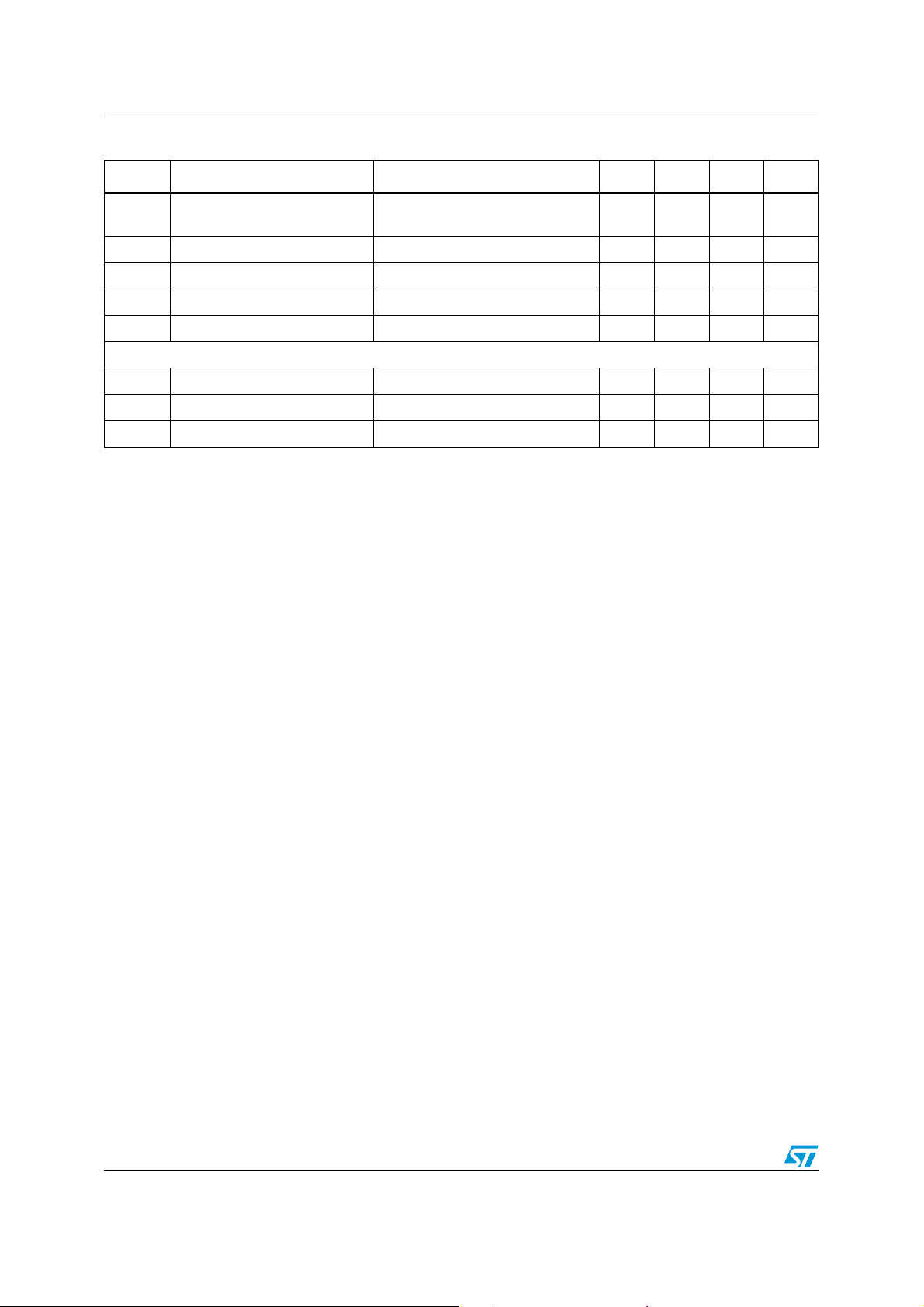
Table 1. Device summary
2
C bus driving with 4 address possibilities:
– Standby
–Play/mute
– Gain 12/26 dB
– Full digital diagnostic (AC and DC loads)
2
C bus
threshold (2 % / 10 %)
2
bus is disabled
C
TDA7575B
with integrated digital diagnostics
PowerSO36
(slug up)
Description
The TDA7575B is a new MOSFET dual bridge
amplifier specially intended for car radio
applications. Thanks to the DMOS output stage
the TDA7575B has a very low distortion allowing
a clear powerful sound.
Among the features, its superior efficiency
performance coming from the internal exclusive
structure, makes it the most suitable device to
simplify the thermal management in high power
sets.The dissipated output power under average
listening condition is in fact reduced up to 50%
when compared to the level provided by
conventional class AB solutions.
This device is equipped with a full diagnostic array
that communicates the status of each speaker
through the I
possibility of driving loads down to 1Ω paralleling
the outputs into a single channel. It is also
possible to disable the I
TDA7575B by means of the usual standby and
mute pins.
2
C bus. The TDA7575B has also the
Flexiwatt27
2
C and control the
Order code Package Packing
TDA7575B Flexiwatt27 Tube
TDA7575BPD PowerSO36 (slug up) Tube
TDA7575BPDTR PowerSO36 (slug up) Tape and reel
December 2009 Doc ID 14103 Rev 2 1/32
www.st.com
1

Contents TDA7575B
Contents
1 Block and pins diagrams . . . . . . . . . . . . . . . . . . . . . . . . . . . . . . . . . . . . . 5
2 Electrical specifications . . . . . . . . . . . . . . . . . . . . . . . . . . . . . . . . . . . . . . 6
2.1 Absolute maximum ratings . . . . . . . . . . . . . . . . . . . . . . . . . . . . . . . . . . . . . 6
2.2 Thermal data . . . . . . . . . . . . . . . . . . . . . . . . . . . . . . . . . . . . . . . . . . . . . . . 6
2.3 Electrical characteristics . . . . . . . . . . . . . . . . . . . . . . . . . . . . . . . . . . . . . . . 6
3 Electrical characteristics curves . . . . . . . . . . . . . . . . . . . . . . . . . . . . . . 11
4 Application circuits . . . . . . . . . . . . . . . . . . . . . . . . . . . . . . . . . . . . . . . . . 15
5 I2C bus interface . . . . . . . . . . . . . . . . . . . . . . . . . . . . . . . . . . . . . . . . . . . 16
5.1 Data validity . . . . . . . . . . . . . . . . . . . . . . . . . . . . . . . . . . . . . . . . . . . . . . . 16
5.2 Start and stop conditions . . . . . . . . . . . . . . . . . . . . . . . . . . . . . . . . . . . . . 16
5.3 Byte format . . . . . . . . . . . . . . . . . . . . . . . . . . . . . . . . . . . . . . . . . . . . . . . . 16
5.4 Acknowledge . . . . . . . . . . . . . . . . . . . . . . . . . . . . . . . . . . . . . . . . . . . . . . 16
5.5 1 W capability setting . . . . . . . . . . . . . . . . . . . . . . . . . . . . . . . . . . . . . . . . 17
5.6 I2C abilitation setting . . . . . . . . . . . . . . . . . . . . . . . . . . . . . . . . . . . . . . . . 18
6 Software specifications . . . . . . . . . . . . . . . . . . . . . . . . . . . . . . . . . . . . . 19
6.1 Examples of bytes sequence . . . . . . . . . . . . . . . . . . . . . . . . . . . . . . . . . . 22
7 Diagnostics functional description . . . . . . . . . . . . . . . . . . . . . . . . . . . . 23
7.1 Turn-on diagnostic . . . . . . . . . . . . . . . . . . . . . . . . . . . . . . . . . . . . . . . . . . 23
7.2 Permanent diagnostics . . . . . . . . . . . . . . . . . . . . . . . . . . . . . . . . . . . . . . . 25
7.3 Output DC offset detection . . . . . . . . . . . . . . . . . . . . . . . . . . . . . . . . . . . . 26
7.4 AC diagnostic . . . . . . . . . . . . . . . . . . . . . . . . . . . . . . . . . . . . . . . . . . . . . . 26
7.5 Multiple faults . . . . . . . . . . . . . . . . . . . . . . . . . . . . . . . . . . . . . . . . . . . . . . 27
7.6 Faults availability . . . . . . . . . . . . . . . . . . . . . . . . . . . . . . . . . . . . . . . . . . . 28
7.7 I2C programming/reading sequences . . . . . . . . . . . . . . . . . . . . . . . . . . . 28
8 Package information . . . . . . . . . . . . . . . . . . . . . . . . . . . . . . . . . . . . . . . . 29
9 Revision history . . . . . . . . . . . . . . . . . . . . . . . . . . . . . . . . . . . . . . . . . . . 31
2/32 Doc ID 14103 Rev 2

TDA7575B List of tables
List of tables
Table 1. Device summary . . . . . . . . . . . . . . . . . . . . . . . . . . . . . . . . . . . . . . . . . . . . . . . . . . . . . . . . . . 1
Table 2. Absolute maximum ratings . . . . . . . . . . . . . . . . . . . . . . . . . . . . . . . . . . . . . . . . . . . . . . . . . . 6
Table 3. Thermal data. . . . . . . . . . . . . . . . . . . . . . . . . . . . . . . . . . . . . . . . . . . . . . . . . . . . . . . . . . . . . 6
Table 4. Electrical characteristics . . . . . . . . . . . . . . . . . . . . . . . . . . . . . . . . . . . . . . . . . . . . . . . . . . . . 6
Table 5. Address selection . . . . . . . . . . . . . . . . . . . . . . . . . . . . . . . . . . . . . . . . . . . . . . . . . . . . . . . . 19
Table 6. IB1 . . . . . . . . . . . . . . . . . . . . . . . . . . . . . . . . . . . . . . . . . . . . . . . . . . . . . . . . . . . . . . . . . . . 19
Table 7. IB2 . . . . . . . . . . . . . . . . . . . . . . . . . . . . . . . . . . . . . . . . . . . . . . . . . . . . . . . . . . . . . . . . . . . 20
Table 8. DB1 . . . . . . . . . . . . . . . . . . . . . . . . . . . . . . . . . . . . . . . . . . . . . . . . . . . . . . . . . . . . . . . . . . . 20
Table 9. DB2 . . . . . . . . . . . . . . . . . . . . . . . . . . . . . . . . . . . . . . . . . . . . . . . . . . . . . . . . . . . . . . . . . . . 21
Table 10. Double fault table for turn-on diagnostic . . . . . . . . . . . . . . . . . . . . . . . . . . . . . . . . . . . . . . . 28
Table 11. Document revision history . . . . . . . . . . . . . . . . . . . . . . . . . . . . . . . . . . . . . . . . . . . . . . . . . 31
Doc ID 14103 Rev 2 3/32

List of figures TDA7575B
List of figures
Figure 1. Block diagram . . . . . . . . . . . . . . . . . . . . . . . . . . . . . . . . . . . . . . . . . . . . . . . . . . . . . . . . . . . . 5
Figure 2. Pins connection diagram (top view) . . . . . . . . . . . . . . . . . . . . . . . . . . . . . . . . . . . . . . . . . . . 5
Figure 3. Quiescent drain current vs. supply voltage . . . . . . . . . . . . . . . . . . . . . . . . . . . . . . . . . . . . . 11
Figure 4. Output power vs. supply voltage . . . . . . . . . . . . . . . . . . . . . . . . . . . . . . . . . . . . . . . . . . . . . 11
Figure 5. Output power vs. supply voltage . . . . . . . . . . . . . . . . . . . . . . . . . . . . . . . . . . . . . . . . . . . . . 11
Figure 6. Output power vs. supply voltage . . . . . . . . . . . . . . . . . . . . . . . . . . . . . . . . . . . . . . . . . . . . . 11
Figure 7. Distortion vs. output power . . . . . . . . . . . . . . . . . . . . . . . . . . . . . . . . . . . . . . . . . . . . . . . . . 11
Figure 8. Distortion vs. output power . . . . . . . . . . . . . . . . . . . . . . . . . . . . . . . . . . . . . . . . . . . . . . . . . 11
Figure 9. Distortion vs. output power . . . . . . . . . . . . . . . . . . . . . . . . . . . . . . . . . . . . . . . . . . . . . . . . . 12
Figure 10. Distortion vs. output power . . . . . . . . . . . . . . . . . . . . . . . . . . . . . . . . . . . . . . . . . . . . . . . . . 12
Figure 11. Distortion vs. output power . . . . . . . . . . . . . . . . . . . . . . . . . . . . . . . . . . . . . . . . . . . . . . . . . 12
Figure 12. Distortion vs. frequency . . . . . . . . . . . . . . . . . . . . . . . . . . . . . . . . . . . . . . . . . . . . . . . . . . . 12
Figure 13. Distortion vs. output voltage (LD mode) . . . . . . . . . . . . . . . . . . . . . . . . . . . . . . . . . . . . . . . 12
Figure 14. Cross talk vs. frequency . . . . . . . . . . . . . . . . . . . . . . . . . . . . . . . . . . . . . . . . . . . . . . . . . . . 12
Figure 15. Cross talk vs. frequency (LD mode) . . . . . . . . . . . . . . . . . . . . . . . . . . . . . . . . . . . . . . . . . . 13
Figure 16. CMRRR vs. frequency . . . . . . . . . . . . . . . . . . . . . . . . . . . . . . . . . . . . . . . . . . . . . . . . . . . . 13
Figure 17. Output attenuation vs. supply voltage (vs. dependent muting) . . . . . . . . . . . . . . . . . . . . . . 13
Figure 18. Output attenuation vs. mute pin voltage . . . . . . . . . . . . . . . . . . . . . . . . . . . . . . . . . . . . . . . 13
Figure 19. Power dissipation vs. output power (4Ω - SINE). . . . . . . . . . . . . . . . . . . . . . . . . . . . . . . . . 13
Figure 20. Power dissipation vs. output power (2Ω - SINE). . . . . . . . . . . . . . . . . . . . . . . . . . . . . . . . . 13
Figure 21. Power dissipation vs. average output power (Audio program simulation, 4Ω) . . . . . . . . . . 14
Figure 22. Power dissipation vs. average output power (Audio program simulation, 2Ω) . . . . . . . . . . 14
Figure 23. ITU R-ARM frequency response, weighting filter for transient pop. . . . . . . . . . . . . . . . . . . 14
Figure 24. Application circuit (TDA7575B) . . . . . . . . . . . . . . . . . . . . . . . . . . . . . . . . . . . . . . . . . . . . . . 15
Figure 25. Application circuit (TDA7575BPD) . . . . . . . . . . . . . . . . . . . . . . . . . . . . . . . . . . . . . . . . . . . 15
Figure 26. Data validity on the I2C bus . . . . . . . . . . . . . . . . . . . . . . . . . . . . . . . . . . . . . . . . . . . . . . . . 16
Figure 27. Timing diagram on the I2C bus. . . . . . . . . . . . . . . . . . . . . . . . . . . . . . . . . . . . . . . . . . . . . . 17
Figure 28. Timing acknowledge clock pulse . . . . . . . . . . . . . . . . . . . . . . . . . . . . . . . . . . . . . . . . . . . . 17
Figure 29. Turn-on diagnostic: working principle . . . . . . . . . . . . . . . . . . . . . . . . . . . . . . . . . . . . . . . . . 23
Figure 30. SVR and output behavior - case 1: without turn-on diagnostic . . . . . . . . . . . . . . . . . . . . . . 23
Figure 31. SVR and output pin behavior - case 2: with turn-on diagnostic . . . . . . . . . . . . . . . . . . . . . 24
Figure 32. Short circuit detection thresholds . . . . . . . . . . . . . . . . . . . . . . . . . . . . . . . . . . . . . . . . . . . . 24
Figure 33. Load detection thresholds - high gain setting . . . . . . . . . . . . . . . . . . . . . . . . . . . . . . . . . . . 24
Figure 34. Load detection thresholds - high gain setting . . . . . . . . . . . . . . . . . . . . . . . . . . . . . . . . . . . 24
Figure 35. Restart timing without diagnostic enable (permanent) . . . . . . . . . . . . . . . . . . . . . . . . . . . . 25
Figure 36. Restart timing with diagnostic enable (permanent). . . . . . . . . . . . . . . . . . . . . . . . . . . . . . . 25
Figure 37. Current detection high: load impedance |Z| vs. output peak voltage . . . . . . . . . . . . . . . . . 27
Figure 38. Current detection low: load impedance |Z| vs. output peak voltage . . . . . . . . . . . . . . . . . . 27
Figure 39. PowerSO36 (slug up) mechanical data and package dimensions . . . . . . . . . . . . . . . . . . . 29
Figure 40. Flexiwatt27 (vertical) mechanical data and package dimensions . . . . . . . . . . . . . . . . . . . . 30
4/32 Doc ID 14103 Rev 2
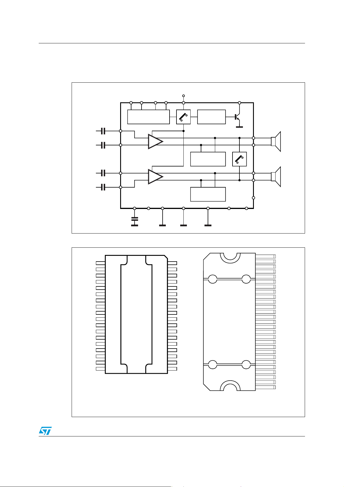
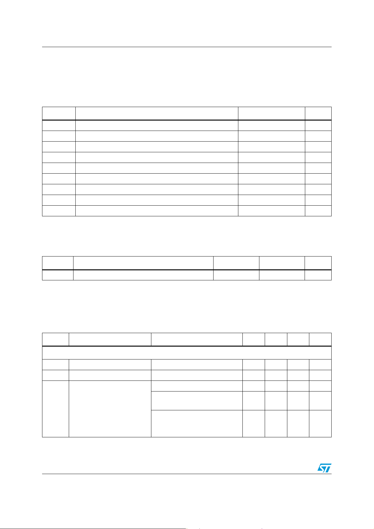
TDA7575B Block and pins diagrams
2
1 Block and pins diagrams
Figure 1. Block diagram
V
ADDRESS
A B CLK
DATA VCC CD_OUT
S
I2CBUS
IN1+
IN1-
SHORT CIRCUIT
PROTECTION
IN2+
IN2-
SHORT CIRCUIT
PROTECTION
SVR S_GND
ST-BY/HE 1Ω MUTE
PW_GND TAB
Figure 2. Pins connection diagram (top view)
OUT1+
OUT1+
VCC
VCC
PWGND
PWGND
OUT1-
OUT1-
OUT2-
OUT2-
PWGND
PWGND
VCC
VCC
OUT2+
OUT2+
36
35
34
33
B
32
31
30
29
28
26
25
A
23
22
21
20
19
D01AU1270
PowerSO36 (slug up)
1
2
3
4
5
6
7
8
9
1027
11
12
1324
14
15
16
17
18
TAB
IN1+
IN1-
MUTE
ST_BY
SGND
DATA
CK
N.C.
N.C.
N.C.
N.C.
SVR
CD-OUT
1-OHM
I2C-EN
IN2-
IN2+
CLIP
DETECTOR
D01AU1269
27
26
25
24
23
22
21
20
19
18
17
16
15
14
13
12
11
10
9
8
7
6
5
4
3
2
1
Flexiwatt27
OUT1+
OUT1-
OUT2+
OUT2-
2
I
C EN
TAB
PWGND
A
OUT2+
N.C.
OUT2-
V
CC
IN2+
IN2-
I2CEN
1Ω
CD_OUT
SVR
CK
DATA
SGND
STT-BY
MUTE
IN1-
IN1+
V
CC
OUT1-
N.C.
OUT1+
B
PWGND
TAB
D03IN151
Doc ID 14103 Rev 2 5/32
Electrical specifications TDA7575B
2 Electrical specifications
2.1 Absolute maximum ratings
Table 2. Absolute maximum ratings
Symbol Parameter Value Unit
T
V
V
V
V
peak
V
CK
DATA
I
O
I
O
P
stg
op
tot
Operating supply voltage 18 V
DC supply voltage 28 V
S
Peak supply voltage (for t = 50 ms) 50 V
CK pin voltage 6 V
Data pin voltage 6 V
Output peak current (not repetitive t = 100 ms) 8 A
Output peak current (repetitive f > 10 Hz) 6 A
Power dissipation T
= 70 °C 86 W
case
, TjStorage and junction temperature -55 to 150 °C
2.2 Thermal data
Table 3. Thermal data
Symbol Parameter PowerSO36 Flexiwatt 27 Unit
R
th j-case
Thermal resistance junction-to-case Max 1 1 °C/W
2.3 Electrical characteristics
VS = 14.4 V; f = 1 kHz; RL = 4 Ω; T
Table 4. Electrical characteristics
= 25 °C unless otherwise specified.
amb
Symbol Parameter Test condition Min. Typ. Max. Unit
Power amplifier
V
Supply voltage range - 8 - 18 V
S
I
Total quiescent drain current - 50 130 200 mA
d
P
o
Output power
Max. power
(1)
THD = 10 %
THD = 1 %; BTL mode
= 2 Ω; THD 10 %
R
L
= 2 Ω; THD 1 %
R
L
= 2 Ω; Max. power
R
L
(1)
35 40 - W
25 28
22
45
50
37
70
75
-W
-W
6/32 Doc ID 14103 Rev 2

TDA7575B Electrical specifications
Table 4. Electrical characteristics (continued)
Symbol Parameter Test condition Min. Typ. Max. Unit
Single channel configuration
P
o
Output power
(1 Ω pin > 2.5 V); RL = 1 Ω;
THD 3 %
Max. power
(1)
80
14084150
-W
THD Total harmonic distortion
P
= 1-12 W; STD mode
o
HE mode; Po = 1-2 W
HE mode; P
P
= 1-12 W, f = 10 kHz - 0.15 0.5 %
o
R
= 2; HE mode; Po = 3 W - 0.03 0.5 %
L
= 4-8 W
o
0.03
-
0.03
0.1
0.1 %
0.5
Single channel configuration
-0.020.1%
-4060μV
-1525μV
50 60 - dB
C
Cross talk Rg = 600 Ω; Po = 1 W 60 75 - dB
T
R
G
ΔG
G
ΔG
E
E
Input impedance - 60 100 130 kΩ
IN
Voltage gain 1 (default) - 25 26 27 dB
V1
Voltage gain match 1 - -1 0 1 dB
V1
Voltage gain 2 - 11 12 13 dB
V2
Voltage gain match 2 - -1 0 1 dB
V2
Output noise voltage gain 1
IN1
Output noise voltage gain 2
IN2
SVR Supply voltage rejection
(1 Ω pin > 2.5 V); R
= 4-30 W
P
o
R
= 600 Ω; Gv = 26 dB
g
= 1;
L
filter 20 to 22 kHz
R
= 600 Ω; Gv = 12d B
g
filter 20 to 22 kHz
f = 100 Hz to 10 kHz; V
= 600 Ω
R
g
= 1 Vpk;
r
BW Power bandwidth (-3 dB) 100 - - KHz
A
I
A
V
V
CMRR Input CMRR V
V
Standby attenuation - 90 100 - dB
SB
Standby current consumption V
SB
Mute attenuation - 80 90 dB
M
Offset voltage Mute and play -45 0 45 mV
OS
Min. supply mute threshold - 7 7.5 8 V
AM
Maximum common mode input
MC
level
= 0 V - 2 10 μA
st-by
= 1 Vpk-pk; Rg = 0 Ω 56 60 dB
CM
f = 1 kHz - - 1 Vrms
SR Slew rate - 1.5 4 - V/μs
ΔV
During mute on/off output offset
voltage
OS
During standby on/off output
offset voltage
ITU R-ARM weighted
see Figure 23
-10 - +10 mV
-10 - +10 mV
Doc ID 14103 Rev 2 7/32
Electrical specifications TDA7575B
Table 4. Electrical characteristics (continued)
Symbol Parameter Test condition Min. Typ. Max. Unit
T
T
V
V
V
V
V
V
V
I
I
V
V
I
I
Turn on delay D2 (IB1) 0 to 1 - 15 40 ms
ON
Turn off delay D2 (IB1) 1 to 0 - 15 40 ms
OFF
Standby pin for standby - 0 - 1.5 V
OFF
Standby pin for standard bridge - 3.5 - 5 V
SB
Standby pin for high-efficiency - 7 - 18 V
HE
Standby pin current 1.5 < V
I
O
Standby pin current V
Mute pin voltage for mute mode - 0 - 1.5 V
m
Mute pin voltage for play mode - 3.5 - 18 V
m
Mute pin current (standby) V
I
m
I
Mute pin current (operative) 0 V < V
m
I2C pin voltage for I2C disabled - 0 - 1.5 V
I2C
I2C pin voltage for I2C enabled - 2.5 - 18 V
I2C
2
CI2C pin current (standby) 0V < I2C EN < 18V, V
2
CI2C pin current (operative) I2C EN <18V, V
1 Ω pin voltage for 2ch mode - 0 - 1.5 V
1Ω
1 Ω pin voltage for 1 Ω mode - 2.5 - 18 V
1Ω
1 Ω pin current (standby) 0 V < 1 Ω <18 V, V
1Ω
1 Ω pin current (operative) 1 Ω < 18 V, V
1Ω
La
< 1.5 V -10 0 10 μA
st-by
= 0 V, V
mute
Low logic level 0 - 1.5 V
< 18 V 7 160 200 μA
st-by/HE
< 1.5V -5 0 5 μA
st-by
mute
< 18 V, V
st-by
> 3.5 V 7 11 15 μA
st-by
> 3.5 V - 65 100 μA
st-by
< 1.5V -5 0 5 μA
stby
>3.5V 7 11 15 μA
< 1.5 V -5 0 5 μA
s-tby
A pin voltage
Ha High logic level 2.5 - 18 V
Ia A pin current (standby) 0V < A < 18V , V
Ia A pin current (operative) A<18V, V
Lb
Low logic level 0 - 1.5 V
st-by
< 1.5 V -5 0 5 μA
stby
> 3.5V 7 11 15 μA
B pin voltage
Hb High logic level 2.5 - 18 V
Ib B pin current (standby) 0 V < B < 18 V, V
Ib B pin current (operative) B < 18 V, V
T
T
I
CDH
I
CDL
Thermal warning - - 150 - °C
W
Thermal protection intervention - - 170 - °C
PI
Clip pin high leakage current CD off, 0 V < VCD < 5.5 V -15 0 15 μA
Clip pin low sink current CD on; VCD < 300 mV 1 mA
st-by
< 1.5 V -5 0 5 μA
s-tby
> 3.5 V 7 11 15 μA
D0 (IB1) = 0 0.8 1.3 2.5 %
CD Clip detect THD level
D0 (IB1) = 1 5 10 15 %
(*) Standby pin high enables I2C bus; Standby pin low puts the device in standby condition. (see “prog” for more details)
8/32 Doc ID 14103 Rev 2
TDA7575B Electrical specifications
Table 4. Electrical characteristics (continued)
Symbol Parameter Test condition Min. Typ. Max. Unit
Turn-on diagnostics (Power amplifier mode)
Pgnd
Short to GND det. (below this
limit, the output is considered in
short circuit to GND)
Power amplifier in standby
condition
--1.2V
Short to Vs det. (above this
Pvs
limit, the output is considered in
-V
-0.9 - - V
s
short circuit to VS)
Normal operation
Pnop
thresholds.(within these limits,
the output is considered
-1.8-V
-1.5 V
s
without faults).
Lsc Shorted load det. - - - 0.5 Ω
Lop Open load det. - 130 - - Ω
Lnop Normal load det. - 1.5 - 70 Ω
Turn-on diagnostics (Line driver mode)
Short to GND det. (below this
Pgnd
limit, the output is considered in
--1.2V
short circuit to GND)
Short to Vs det. (above this
Pvs
limit, the Output is considered
V
-0.9 - - V
s
in Short Circuit to VS)
Pnop
Normal operation
thresholds.(within these limits,
the output is considered
Power amplifier in standby
1.8 - V
-1.5 V
s
without faults).
Lsc Shorted load det. - - 1.5 Ω
Lop Open load det. 400 - - Ω
Lnop Normal load det. 4.5 - 200 Ω
Permanent diagnostics (Power amplifier mode or line driver mode)
Pgnd
Pvs
Short to GND det. (below this
limit, the output is considered in
short circuit to GND)
Short to Vs det. (above this
limit, the Output is considered
in Short Circuit to VS)
Power amplifier in Mute or Play
condition, one or more short
circuits protection activated
-
--1.2V
Vs -
0.9
--V
Normal operation
Pnop
thresholds.(Within these limits,
the Output is considered
-1.8-V
-1.5 V
s
without faults).
Pow. amp. mode - - 0.5 Ω
Lsc Shorted load det.
Line driver mode - - 1.5 Ω
Doc ID 14103 Rev 2 9/32
Electrical specifications TDA7575B
Table 4. Electrical characteristics (continued)
Symbol Parameter Test condition Min. Typ. Max. Unit
V
I
I
I
OLH
I
2
C bus interface
I
f
SCL
V
V
1. Saturated sqare wave output.
Offset detection
O
Normal load current detection VO < (VS - 5)pk IB2 (D0) = 0 500 - - mA
NLH
Normal load current detection VO < (VS - 5)pk IB2 (D0) = 1 250 - - mA
NLL
Open load current detection VO < (VS - 5)pk IB2 (D0) = 0 - - 250 mA
Open load current detection VO < (VS - 5)pk IB2 (D0) =1 - - 125 mA
OLL
Clock frequency - - - 400 kHz
Input low voltage - - - 1.5 V
IL
Input high voltage - 2.3 - - V
IH
Power amplifier in play condition
AC input signals = 0
±1.5 ±2 ±2.5 V
10/32 Doc ID 14103 Rev 2
 Loading...