

TDA7562
MULTIFUNCTION QUAD POWER AMPLIFIER
WITH BUILT-IN DIAGNOSTICS FEATURES
■ DMOS POWER OUTPUT
■ HIGH OUTPUT POWER CAPABILITY 4x25W/
4Ω @ 14.4V, 1KHZ, 10% THD, 4x35W EIAJ
■ MAX. OUTPUT POWER 4x60W/2Ω
■ FULL I
2
C BUS DRIVING:
–ST-BY
– INDEPENDENT FRONT/REAR SOFT PLAY/
MUTE
– SELECTABLE GAIN 30dB - 16dB (FOR
LOW NOISE LINE OUTPUT FUNCTION)
2
–I
C BUS DIGITAL DIAGNOSTICS
■ FULL FAULT PROTECTION
■ DC OFFSET DETECTION
■ FOUR INDEPENDENT SHORT CIRCUIT
PROTECTION
■ CLIPPING DETECTOR PIN WITH
SELECTABLE THRESHOLD (2%/10%)
■ ST-BY/MUTE PIN
■ ESD PROTECTIO N
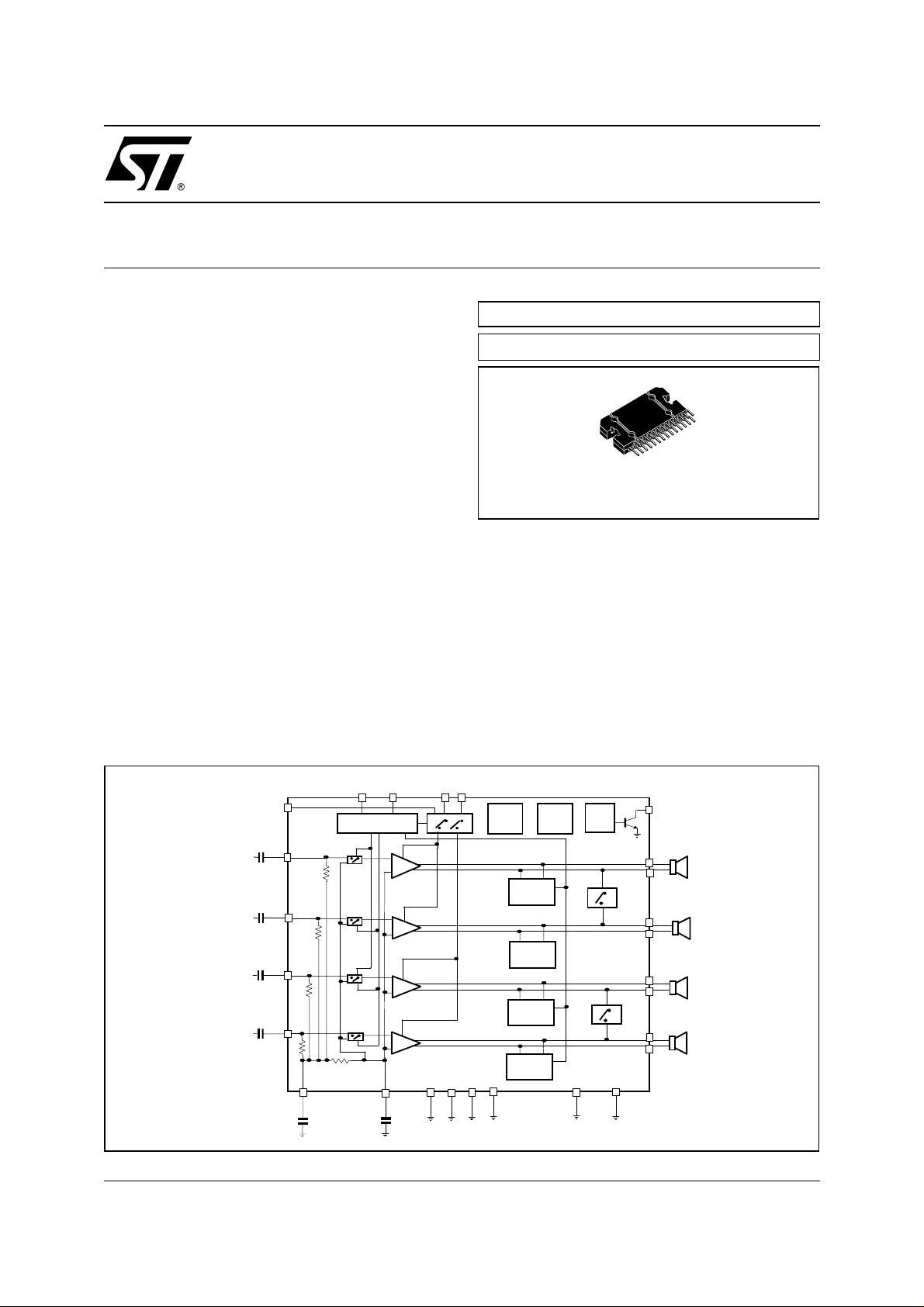
DESCRIPTION
The TDA7562 is a new BCD technology Quad
BLOCK DIAGRAM
MULTIPOWER BCD TECHNOLOGY
MOSFET OUTPUT POWER STAGE
FLEXIWATT27 (Vertical)
Bridge type of car radio amplifier in Flexiwatt27V
package specially intended for car radio applications. Thanks to the DMOS output stage the
TDA7562 has a very low distortion allowing a clear
powerful sound. This device is equipped with a full
diagnostics array that communicates the status of
each speaker through the I
to control the configuratio n and the behaviour of
the device by means of the I
2
C bus.The possibility
2
C bus makes
TDA7562 a very flexible machine.
May 2003
ST-BY/MUTE
IN RF
IN RR
IN LF
IN LR
SVR
CLK
DATA
VCC1 VCC2
Thermal
I2CBUS
Mute1 Mute2
F
R
F
R
AC_GND
16/30dB
16/30dB
16/30dB
16/30dB
RF
RR
PW_GND
Protection
& Dump
LF LR
Reference
Short Circuit
Protection &
Diagnostic
Short Circuit
Protection &
Diagnostic
Short Circ uit
Protection &
Diagnostic
Short Circuit
Protection &
Diagnostic
TAB
Clip
Detector
CD_OUT
OUT RF+
OUT RFOUT RR+
OUT RR-
OUT LF+
OUT LFOUT LR+
OUT LR-
S_GND
1/17
TDA7562
0
ABSOLUTE MAXIMUM RATINGS
Symbol Parameter Value Unit
V
op
V
V
peak
V
CK
V
DATA
I
O
I
O
P
tot
T
stg
THERMAL DATA
Symbol Parameter Value Unit
R
th j-case
Operating Supply Voltage 18 V
DC Supply Voltage 28 V
S
Peak Supply Voltage (for t = 50ms) 50 V
CK pin Voltage 6 V
Data Pin Voltage 6 V
Output Peak Current (not repetitive t = 100µs) 8 A
Output Peak Current (repetitive f > 10Hz) 6 A
Power Dissipation T
= 70°C 85 W
case
, TjStorage and Junction Temperature -55 to 150 °C
Thermal Resistance Junction to case
Max.
1 °C/W
PIN CONNECTION
(Top view)
27
26
25
24
23
22
21
20
19
18
17
16
15
14
13
12
11
10
9
8
7
6
5
4
3
2
1
TAB
DATA
PW_GND RR
OUT RRCK
OUT RR+
V
CC2
OUT RFPW_GND RF
OUT RF+
AC GND
IN RF
IN RR
S_GND
IN LR
IN LF
SVR
OUT LF+
PW_GND LF
OUT LFV
CC1
OUT LR+
CD-OUT
OUT LRPW_GND LR
STBY
TAB
D00AU123
2/17
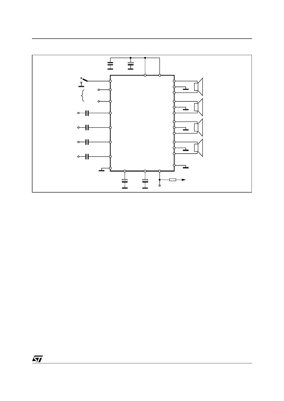
Figure 1. Application Circuit
TDA7562
V(4V .. V
I2C BUS
IN RF
IN RR
IN LF
IN LR
)
CC
DATA
CLK
C1 0.22µF
C2 0.22µF
C3 0.22µF
C4 0.22µF
C8
0.1µF
S-GND
C7
3300µF
Vcc1 Vcc2
2
26
23
16
15
12
13
17 11 5
14
C5
1µF
C6
10µF
721
18
19
20
22
25
24
10
9
8
6
3
4
1, 27
47K
CD OUT
+
+
+
+
TAB
OUT RF
OUT RR
OUT LF
OUT LR
V
D00AU1231A
3/17
TDA7562
ELECTRICAL CHARACTERISTICS
(Refer to the test circuit, V
= 14.4V; RL = 4Ω; f = 1KHz; T
S
= 25°C; unless otherwise specified.)
amb
Symbol Parameter Test Condition Min. Typ. Max. Unit
POWER AMPLIFIER
V
P
THD Total Harmonic Distortion P
Supply Voltage Range 8 18 V
S
I
Total Quiescent Drain Current 150 300 mA
d
Output Power EIAJ (VS = 13.7V) 32 35 W
O
THD = 10%
THD = 1%
= 2Ω; EIAJ (VS = 13.7V)
R
L
RL = 2Ω; THD 10%
R
= 2Ω; THD 1%
L
RL = 2Ω; MAX POWER
= 1W to 10W; f = 1kHz 0.04 0.1 %
O
22 25
20
50
32
55
38
30
60
PO = 1-10W, f = 10kHz 0.02 0.5 %
G
= 16dB; VO = 0.1 to 5VRMS 0.02 0.05 %
V
C
R
G
∆G
G
∆G
E
E
Cross Talk f = 1KHz to 10KHz, Rg = 600Ω 50 60 dB
T
Input Impedance 60 100 130 KΩ
IN
Voltage Gain 1 29.5 30 30.5 dB
V1
Voltage Gain Match 1 -1 1 dB
V1
Voltage Gain 2 15.5 16 16.5 dB
V2
Voltage Gain Match 2 -1 1 dB
V2
Output Noise Voltage 1 Rg = 600Ω 20Hz to 22kHz 50 100 µV
IN1
Output Noise Voltage 2 Rg = 600Ω; GV = 16dB
IN2
15 30 µV
20Hz to 22kHz
SVR Supply Voltage Rejection f = 100Hz to 10kHz; V
R
= 600Ω
g
= 1Vpk;
r
50 60 dB
BW Power Bandwidth 100 KHz
A
I
A
V
V
T
T
V
V
V
I
CD
CD
CD
Stand-by Attenuation 90 110 dB
SB
Stand-by Current 2 100 µA
SB
Mute Attenuation 80 100 dB
M
Offset Voltage Mute & Play -100 0 100 mV
OS
Min. Supply Mute Threshold 7 7.5 8 V
AM
Turn ON Delay D2/D1 (IB1) 0 to 1 5 20 ms
ON
Turn OFF Delay D2/D1 (IB1) 1 to 0 5 20 ms
OFF
St-By/Mute pin for St-By 0 1.5 V
SBY
St-By/Mute pin for Mute 3.5 5 V
MU
St-By/Mute pin for Operating 7 V
OP
St-By/Mute pin Curren t V
MU
Clip Det High Leakage Current CD off 0 15 µA
LK
Clip Det Sat. Voltage CD on; ICD = 1mA 300 mV
SAT
Clip Det THD level D0 (IB1) = 1 5 10 15 %
THD
STBY/MUTE
V
STBY/MUTE
= 8.5V 20 40 µA
< 1.5V 0 10 µA
S
D0 (IB1) = 0 1 2 3 %
W
W
W
W
W
W
V
4/17
TDA7562
ELECTRICAL CHARACTERISTICS
(Refer to the test circuit, V
= 14.4V; RL = 4Ω; f = 1KHz; T
S
(continued)
= 25°C; unless otherwise specified.)
amb
Symbol Parameter Test Condition Min. Typ. Max. Unit
DIAGNOSTICS (Power Amplifier Mode or Line Driver Mode)
Pgnd Short to GND det. (below this
limit, the Output is considered in
Short Circuit to GND)
Pvs Short to V
det. (above this limit,
S
Power Amplifier in Mute or Play,
one or more short circuits
protection activated
1.2 V
Vs -1.2 V
the Output is considered in Short
Circuit to V
Pnop Normal operation thresholds.
)
S
1.8 Vs -1.8 V
(Within these limits, the Output is
considered witho ut faults).
Lsc Shorted Load det. Power Amplifier Mode 0.5 Ω
Line Driver Mode 1.5 Ω
V
Offset Detection ±1.5 ±2 ±2.5 V
O
I2C BUS INTERFACE
f
V
SCL
V
Clock Frequency 400 KHz
Input Low Voltage 1.5 V
IL
Input High Voltage 2.3 V
IH
5/17
TDA7562
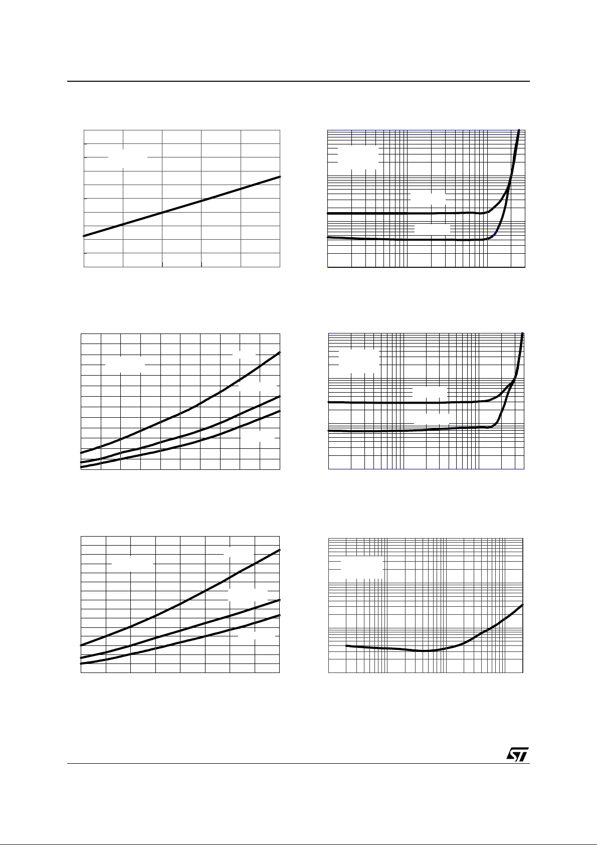
Figure 2. Quiescent Current vs. Supply Voltage
Id (mA)
250
230
210
190
170
150
130
110
90
70
50
Vin = 0
NO LOADS
8 10 121 41 6 18
Vs (V)
Figure 3. Output Power vs. Supply Voltage (4Ω)
Po (W)
70
65
60
55
50
45
40
35
30
25
20
15
10
5
RL = 4 Ohm
f = 1 KHz
8 9 10 11 12 13 14 15 16 17 18
Vs (V)
Po-max
THD = 10 %
THD = 1 %
Figure 5.
10
1
0.1
0.01
Figure 6.
10
1
0.1
0.01
Distortion vs. Output Power (4Ω)
THD (%)
Vs = 14.4 V
RL = 4 Ohm
f = 10 KHz
f = 1 KHz
0.1 1 10
Po (W)
Distortion vs. Output Power (2Ω)
THD (%)
Vs = 14.4 V
RL = 2 Ohm
f = 10 KHz
f = 1 KHz
0.1 1 10
Po (W)
Figure 4. Output Power vs. Supply Voltage (2Ω)
Po (W)
80
75
70
65
60
55
50
45
40
35
30
25
20
15
10
5
8 9 10 11 12 13 14 15 16
RL = 2 Ohm
f = 1 KHz
Vs (V)
6/17
Po-max
THD = 10 %
THD = 1 %
Figure 7.
10
1
0.1
0.01
Distortion vs. Output Power (4Ω)
THD (%)
Vs = 14.4 V
RL = 4 Ohm
Po = 4 W
10 100 1000 10000
f (Hz)

TDA7562
Figure 8. Distortion vs. Frequency (2Ω)
THD (%)
10
Vs = 14.4 V
RL = 2 Ohm
1
Po = 8 W
0.1
0.01
10 100 1000 10000
f (Hz)
Figure 9. Crosstalk vs. Frequency
CROSSTALK (dB)
90
80
70
60
RL = 4 Ohm
Po = 4 W
50
Rg = 600 Ohm
40
30
20
10 100 1000 10000
f (Hz)
Figure 11. Power Dissipation & Efficiency vs.
Output Power (4Ω, STD, SINE)
Ptot (W)
90
Vs = 14.4 V
80
RL = 4 x 4 Ohm
f = 1 KHz SINE
70
60
50
40
30
20
10
0
0 2 4 6 8 10 12 14 16 18 20 22 24 26
Po (W)
n (%)
n
Ptot
Figure 12. Power Dissipation vs. Average
Ouput Po wer (Audio Progr a m
Simulation, 4Ω)
Ptot (W)
45
40
Vs = 14 V
RL = 4 x 4 Ohm
GAUSSIAN NOISE
35
30
25
20
15
10
5
01
2
Po (W)
CLIP
START
345
90
80
70
60
50
40
30
20
10
0
Figure 10. Supply Voltage Rejection vs. Freq.
SVR (dB)
90
80
70
60
50
Rg = 600 Ohm
40
Vripple= 1 Vpk
30
20
10 100 1000 10000
f (Hz)
Figure 13. Power Dissipation vs. Average
Ouput Power (Au dio Pr og ram
Simulati on, 2Ω )
Ptot (W)
90
80
Vs = 14 V
RL = 4 x 2 Ohm
70
GAUSSIAN NOISE
60
50
40
30
20
10
0
012345678
Po (W)
CLIP
START
7/17

TDA7562
DIAGNOSTICS FUNCTIONAL DESCRIPTION:
Detectable conventional faults are:
– SHORT TO GND
– SHORT TO Vs
– SHORT ACROSS THE SPEAKER
The following additional features are provided:
– OUTPUT OFFSET DETECTION
The TDA7562 has 2 operating statuses:
1)) RESTART mode. The diagnostic is not enabled. Each audio channel operates independently from each other. If any of the a.m. faults occurs, only the channel(s) interested is shut down. A check of the output status
is made every 1 ms (fig. 14). Restart takes place when the overload is removed.
2)) DIAGNOSTIC mode. It is enabled via I2C bus and self activates if an output overload (such to cause the
intervention of the short-circuit protection) occurs to the speakers outputs . Once activated, the diagnostics
procedure develops as follows (fig. 15):
– To avoid momentary re-circulation spikes from giving erroneous diagnostics, a check of the output
status is made after 1ms: if normal situation (no overloads) is detected, the diagnostic is not performed and the channel returns back active.
– Instead, if an overload is det ected during the chec k af te r 1 m s, then a d iagnost ic c ycle hav ing a du-
ration of about 100 ms is started.
– After a diagnostic cycle, the audio channel interested by the fault is switched to RESTART mode. The
relevant data are stored inside the device and can be read by the microprocessor. When one cycle
has terminated, the next one is activated by an I2C reading. This is to ensure continuous diagnostics
throughout the car-radio operating time.
– To check the status of the device a sampling system is needed. The timing is chosen at microproces-
sor level (over half a second is recommended).
Figure 14. Restart timing without Diagnostic Enable (Each 1mS time, a sampling of the fault is done)
Out
1mS
t
Short circui t removed
Overcurrent and short
circuit protection intervention
(i.e. short circuit to GND)
1-2mS
1mS 1mS 1mS
Figure 15. Restart timing with Diagnostic Enable
1mS 100mS 1mS1mS
t
Overcurrent and short
(i.e. short circuit to GND)
Short circuit removed
8/17

TDA7562
As for SHORT TO GND / Vs the fault-detection thresholds r emai n unchanged from 30 dB to 16 dB gain s etting.
They are as follows:
S.C. to GND x S.C. to Vs
0V 1.8V VS-1.8V V
1.2V VS-1.2V
xNormal Operation
D01AU1253
S
Concerning SHORT ACROSS THE SPEAKER , the threshold varies from 30 dB to 16 dB gain setting, since
different loads are expected (either normal speaker's impedance or high impedance). The values in case of 30
dB gain are as follows:
S.C. across Load x
0V 1.5Ω Infinite
0.5Ω
Normal Operation
D01AU1254mod
If the Line-Driver mode (Gv= 16 dB and Line Driver Mode diagnostic = 1) is selected, the same thresholds will
change as follows:
S.C. across Load x
Normal Operation
0Ω 4.5Ω infinite
1.5Ω
D01AU1252mod
OUTPUT DC OFFSET DETECTION
Any DC output offset exceeding ± 2V are signalled out. This inconvenient might occur as a conse quence of initially defective or aged and worn-out input capacitors feeding a DC component to the inputs, so putting the
speakers at risk of overheating.
This diagnostic has to be performed with low-level output AC signal (or Vin = 0).
The test is run with selectable time duration by microprocessor (from a "start" to a "stop" command):
– START = Last reading operation or setting IB1 - D5 - (OFFSET enable) to 1
– STOP = Actual reading operation
Excess offset is signalled out if persistent throughout the assigned testing time. This feature is disabled if any
overloads leading to activation of the short-circuit protection occurs in the process.
MULTIPLE FAULTS
When more misconnections are simultaneously in place at the audio outputs, it is guaranteed that at least one
of them is initially read out. The others are notified after successive cycles of I
2
C reading and faults removal,
provided that the diagnostic is enabled.
The table below shows all the coupl es of double-fault po ssible. It sh ould be taken int o account that a short ci rcuit
9/17

TDA7562
with the 4 ohm speaker unconnected is considered as double fault.
Double fault table for Turn On Diagnostic
S. GND (so) S. GND (sk) S. Vs S. Across L.
S. GND (so) S. GND S. GND S. Vs + S. GND S. GND
S. GND (sk) / S. GND S. Vs S. GND
S. Vs / / S. Vs S. Vs
S. Across L. / / / S. Across L.
S. GND (so) / S. GND (sk) in the above table make a distinction according to which of the 2 outputs is shorted
to ground (test-current source side= so, test-current sink side = sk). More precisely, so = CH+, sk = CH-.
FAULTS AVAILABILITY
All the results coming from I2Cbus, by read operations, are the consequence of measurements inside a defined
period of time. If the fault is stable throughout the whole period, it will be sent out.
2
To guarantee always resident functions, every kind of diagnostic cycles will be reactivate after any I
operation. So, when the micro reads the I
the previous diag. cy cle (i.e. The devic e is in turned On, with a short to G nd, then the short is removed and m icro
2
reads I
reading operation occurs, the bytes do not show the sh ort). In gener al to observe a change in Diagnos tic by tes,
two I
C. The short to Gnd is still present in bytes, because it is the result of the previous cycle. If another I2C
2
C reading operations are necessary.
2
C, a new cycle will be able to start, but the read data will come from
C reading
I2C PROGRAMMING/READING SEQUENCES
A correct turn on/off sequenc e respectful of the di agnostic timings and pr oducing no audible noises could be as
follows (after battery connection):
TURN-ON: PIN2 > 7V --- 10ms --- (STAND-BY OUT + DIAG ENABLE) --- 500 ms (min) --- MUTING O UT
TURN-OFF: MUTING IN --- 20 ms --- (DIAG DISABLE + STAND-BY IN) --- 10ms --- PIN2 = 0
Car Radio Installation: PIN2 > 7V --- 10ms DIAG ENABLE (write) --- 200 ms --- I
2
C read (repeat until All faults
disappear).
OFFSET TEST: Device in Play (no signal) -- OFFSET ENABLE - 30ms - I
2
C reading (repeat I2C reading until
high-offset message disappears).
FAST MUTING
The muting time can be shortened to less than 1ms by setti ng (IB2) D5 = 1. This option can be useful in trans ient
battery situations (i.e. during car engine cranking) to quickly turnoff the amplifier for avoiding any audible effects
caused by noise/transients being injected by preamp stages.
10/17

TDA7562
I2C BUS INTERFACE
Data transmis sion f rom microp rocesso r to the TDA7562 and vi ceve rsa take s place thr ough the 2 wi res I2C BUS interface, consisting of the two lines SDA and SCL (pull-up resistors to positive supply voltage must be connected).
Data Validity
As shown by fig. 16, the data on the SDA line must be s table during the hig h period of the cloc k. The HIGH and
LOW state of the data line can only change when the clock signal on the SCL line is LOW.
Start and Stop Conditions
As shown by fig. 17 a start condition is a HIGH to LOW transition of the SDA line while SCL is HIGH. The stop
condition is a LOW to HIGH transition of the SDA line while SCL is HIGH.
Byte Format
Every byte transferred to the SDA line must contain 8 bits. Each byte must be followed by an acknowledge bit.
The MSB is transferred first.
Acknowledge
The transmitter* puts a resistive HIGH level on the SDA line during the acknowledge clock pulse (see fig. 18).
The receiver** the acknowledges has to pull -down (LOW) the SDA line during the acknowle dge clock pul se, so
that the SDAline is stable LOW during this clock pulse.
* Transmitter
–master (µP) when it writes an address to the TDA7562
– slave (TDA7562) when the µP reads a data byte from TDA7562
** Receiv er
– slave (TDA7562) when the µP writes an address to the TDA7562
–master (µP) when it reads a data byte from TDA7562
Figure 16. Data Validity on the I
SDA
SCL
2
CBUS
DATA LINE
STABLE, DATA
Figure 17. Timing Diagram on the I
SCL
SDA
START
Figure 18. Acknowledge on the I
SCL
2
1
CHANGE
VALID
2
CBUS
DATA
ALLOWED
D99AU1032
D99AU1031
STOP
CBUS
23789
2
I
CBUS
SDA
START
MSB
D99AU1033
ACKNOWLEDGMENT
FROM RECEIVER
11/17

TDA7562
SOFTWARE SPECIFICATIONS
All the functions of the TDA7562 are activated by I2C interface.
µ
The bit 0 of the "ADDRESS BYTE" defines if the next bytes are write instruction (from
instruction (from TDA7562 to
µ
P).
Chip Address:
D7 D0
1101100XD8 Hex
X = 0 Write to device
X = 1 Read from device
If R/W = 0, the
µ
P sends 2 "Instruction Bytes": IB1 and IB2.
IB1
D7 X
D6
D5
D4
D3
D2
D1
D0
Diagnostic enable (D6 = 1)
Diagnostic defeat (D6 = 0)
Offset Detection enable (D5 = 1)
Offset Detection defeat (D5 = 0)
Front Channel
Gain = 30dB (D4 = 0)
Gain = 16dB (D4 = 1)
Rear Channel
Gain = 30dB (D3 = 0)
Gain = 16dB (D3 = 1)
Mute front channels (D2 = 0)
Unmute front channels (D2 = 1)
Mute rear channels (D1 = 0)
Unmute rear channels (D1 = 1)
CD 2% (D0 = 0)
CD 10% (D0 = 1)
P to TDA7562) or read
IB2
D7 X
D6 used for testing
D5
D4
D3
D2 X
D1 X
D0 X
12/17
Normal muting time (D5 = 0)
Fast muting time (D5 = 1)
Stand-by on - Amplifier not working - (D4 = 0)
Stand-by off - Amplifier working - (D4 = 1)
Power amplifier mode diagnostic (D3 = 0)
Line driver mode diagnostic (D3 = 1)

If R/W = 1, the TDA7562 sends 4 "Diagnostics Bytes" to µP: DB1, DB2, DB3 and DB4.
DB1
D7 Thermal warning active (D7 = 1)
TDA7562
DB2
D6
D5 X
D4 X
D3
D2
D1
D0
D7
D6 X
Diag. cycle not activated or not terminated (D6 = 0)
Diag. cycle terminated (D6 = 1)
Channel LF
Normal load (D3 = 0)
Short load (D3 = 1)
Channel LF
No output offset (D2 = 0)
Output offset detection (D2 = 1)
Channel LF
No short to Vcc (D1 = 0)
Short to Vcc (D1 = 1)
Channel LF
No short to GND (D1 = 0)
Short to GND (D1 = 1)
Offset detection not activated (D7 = 0)
Offset detection activated (D7 = 1)
D5 X
D4 X
D3 Channel LR
D2 Channel LR
D1 Channel LR
D0 Channel LR
Normal load (D3 = 0)
Short load (D3 = 1)
No output offset (D2 = 0)
Output offset detection (D2 = 1)
No short to Vcc (D1 = 0)
Short to Vcc (D1 = 1)
No short to GND (D1 = 0)
Short to GND (D1 = 1)
13/17
TDA7562
B3
D7 Stand-by status (= IB1 - D4)
D6 Diagnostic status (= IB1 - D6)
D5 X
D4 Channel RF
D3 Channel RF
D2 Channel RF
D1 Channel RF
D0 Channel RF
DB4
D7 X
D6 X
D5 X
D4 X
Turn-on diagnostic (D4 = 0)
X
Normal load (D3 = 0)
Short load (D3 = 1)
No output offset (D2 = 0)
Output offset detection (D2 = 1)
No short to Vcc (D1 = 0)
Short to Vcc (D1 = 1)
No short to GND (D1 = 0)
Short to GND (D1 = 1)
D3 Channel RR
RNormal load (D3 = 0)
Short load (D3 = 1)
D2 Channel RR
No output offset (D2 = 0)
Output offset detection (D2 = 1)
D1 Channel RR
D0 Channel RR
14/17
No short to Vcc (D1 = 0)
Short to Vcc (D1 = 1)
No short to GND (D1 = 0)
Short to GND (D1 = 1)

TDA7562
Examples of bytes sequence
- Turn-On of the power amplifier with 30dB gain, mute on, diagnostic defeat, CD = 2%.
1
Start Address byte with D0 = 0 ACK IB1 ACK IB2 ACK STOP
X0000000 XXX1XX1 1
2
- Turn-Off of the power amplifier
Start Address byte with D0 = 0 ACK IB1 ACK IB2 ACK STOP
X0XXXXXX XXX0 XXX X
3
- Offset detection procedure enable
Start Address byte with D0 = 0 ACK IB1 ACK IB2 ACK STOP
XX1XX11X XXX1XXXX
4
- Offset detection procedure stop and reading operation (the results are valid only for the offset detection bits
(D2 of the bytes DB1, DB2, DB3, DB4).
Start Address byte with D0 = 1 ACK DB1 ACK DB2 ACK DB3 ACK DB4 ACK STOP
■ The purpose of this test is to check if a D.C. off set (2V typ.) i s present on the outputs, produced by input
capacitor with anomalous leackage current or humidity between pins.
■ The delay from 4 to 5 can be selected by software, starting from T.B.D. ms
15/17

TDA7562
DIM.
MIN. TYP. MAX . MIN. TYP. MAX.
mm inch
A 4.45 4.50 4.65 0.175 0.177 0.183
B 1.80 1.90 2.00 0.070 0.074 0.079
C 1.4 0 0.055
D 0.75 0.90 1.05 0.029 0.035 0.041
E 0.37 0.39 0.42 0.014 0.015 0.0 16
F (1) 0.57 0.022
G 0.80 1.00 1.20 0.031 0.040 0.047
G1 25.75 26.00 26.25 1.014 1.023 1.033
H (2) 28.90 29.23 29.30 1.139 1.150 1.153
H1 17.00 0.669
H2 12.80 0.503
H3 0.80 0.031
L (2) 22.07 22.47 22.87 0.869 0.884 0.904
L1 18.57 18.97 19.37 0.731 0.747 0.762
L2 (2) 15.50 15.70 15.90 0.610 0.618 0.626
L3 7.70 7.85 7.95 0.303 0.309 0.313
L4 5 0.197
L5 3.5 0.138
M 3.70 4.00 4.30 0.145 0.157 0.169
M1 3.60 4.00 4.40 0.142 0.157 0.173
N 2.20 0.086
O 2 0.079
R 1.70 0.067
R1 0.5 0.02
R2 0.3 0.12
R3 1.25 0.049
R4 0.50 0.019
V 5˚ (Typ.)
V1 3˚ (Typ.)
V2 20˚ (Typ.)
V3 45˚ (Typ.)
(1): dam-bar protusio n not included
(2): molding protusion i ncluded
OUTLINE AND
MECHANICAL DA T A
Flexiwatt27 (vertical)
L2
V
C
B
H
V3
H3
OL3 L4
Pin 1
G
H1
G1
H2
R3
R4
N
V2
F
V
A
V1
R2
R
L
L1
V1
R2
FLEX27ME
L5
R1
R1 R1
M
D
E
M1
7139011
16/17

TDA7562
Information furnished is believed to be accurate and reliable. However, STMicroelectronics assumes no responsibility for the consequences
of use of such information nor for any infringement of patents or other rights of third parties which may result from its use. No license is granted
by implic ation or oth erwise under any patent or patent rights of STMicroelectronic s. Specific ations mentioned in th i s publication are subject
to change without notice. This publication supersedes and replaces all information previously supplied. STMicroelectronics products are not
authorized for use as critical components in life support devi ces or systems wi t hout express written approval of STMicroelectronics.
The ST logo is a registered trademark of STMicroelectronics
2003 STMicroelectr oni cs - All Righ ts Reserved
Austra lia - Brazil - Canada - Chi na - Finland - France - Germa ny - Hong Kong - India - Israel - I taly - Japan -Malaysia - Ma lta - Morocco -
Singap ore - Spain - Sw eden - Switze rl and - United K i ngdom - United States.
STMicroelectronics GROUP OF COMPANIES
http://www.s t. com
17/17
 Loading...