

ST TDA7560 User Manual
4 x 50 W quad bridge car radio amplifier
Feature
■ Superior output power capability:
–4 x 50 W/4 Ω max.
–4 x 45 W/4 Ω EIAJ
–4 x 30 W/4 Ω @ 14.4 V, 1 kHz, 10 %
–4 x 80 W/2 Ω max.
–4 x 77 W/2 Ω EIAJ
–4 x 55 W/2 Ω @ 14.4 V, 1 kHz, 10 %
■ Multipower BCD technology
■ MOSFET output power stage
■ Excellent 2 Ω driving capability
■ Hi-Fi class distortion
■ Low output noise
■ Standby function
■ Mute function
■ Automute at min. supply voltage detection
■ Low external component count:
– Internally fixed gain (26 dB)
– No external compensation
– No bootstrap capacitors
■ On board 0.35 A high side driver
Protections
■ Output short circuit to GND, to V
load
■ Very inductive loads
Table 1. Device summary
, across the
S
TDA7560
Flexiwatt25
(vertical)
■ Overrating chip temperature with soft thermal
limiter
■ Output DC offset detection
■ Load dump voltage
■ Fortuitous open GND
■ Reversed battery
■ ESD
Description
The TDA7560 is a breakthrough BCD (Bipolar /
CMOS / DMOS) technology class AB audio power
amplifier in Flexiwatt 25 package designed for
high power car radio.
The fully complementary P-Channel/N-Channel
output structure allows a rail to rail output voltage
swing which, combined with high output current
and minimized saturation losses sets new power
references in the car-radio field, with unparalleled
distortion performances.
Flexiwatt25
(horizontal)
Order code Package Packing
TDA7560 Flexiwatt25 (vertical) Tube
TDA7560H Flexiwatt25 (horizontal) Tube
November 2008 Rev 4 1/17
www.st.com
1

Contents TDA7560
Contents
1 Block and pin connection diagram . . . . . . . . . . . . . . . . . . . . . . . . . . . . . 5
2 Electrical specifications . . . . . . . . . . . . . . . . . . . . . . . . . . . . . . . . . . . . . . 6
2.1 Absolute maximum ratings . . . . . . . . . . . . . . . . . . . . . . . . . . . . . . . . . . . . . 6
2.2 Thermal data . . . . . . . . . . . . . . . . . . . . . . . . . . . . . . . . . . . . . . . . . . . . . . . 6
2.3 Electrical characteristics . . . . . . . . . . . . . . . . . . . . . . . . . . . . . . . . . . . . . . . 6
2.4 Standard test and application circuit, and PCB layout . . . . . . . . . . . . . . . . 8
2.5 Electrical characteristics curves . . . . . . . . . . . . . . . . . . . . . . . . . . . . . . . . 10
3 Application hints . . . . . . . . . . . . . . . . . . . . . . . . . . . . . . . . . . . . . . . . . . . 13
3.1 SVR . . . . . . . . . . . . . . . . . . . . . . . . . . . . . . . . . . . . . . . . . . . . . . . . . . . . . 13
3.2 Input stage . . . . . . . . . . . . . . . . . . . . . . . . . . . . . . . . . . . . . . . . . . . . . . . . 13
3.3 Standby and muting . . . . . . . . . . . . . . . . . . . . . . . . . . . . . . . . . . . . . . . . . 13
3.4 DC offset detector . . . . . . . . . . . . . . . . . . . . . . . . . . . . . . . . . . . . . . . . . . 13
3.5 Heatsink definition . . . . . . . . . . . . . . . . . . . . . . . . . . . . . . . . . . . . . . . . . . 13
4 Package information . . . . . . . . . . . . . . . . . . . . . . . . . . . . . . . . . . . . . . . . 14
5 Revision history . . . . . . . . . . . . . . . . . . . . . . . . . . . . . . . . . . . . . . . . . . . 16
2/17

TDA7560 List of tables
List of tables
Table 1. Device summary . . . . . . . . . . . . . . . . . . . . . . . . . . . . . . . . . . . . . . . . . . . . . . . . . . . . . . . . . . 1
Table 2. Absolute maximum ratings . . . . . . . . . . . . . . . . . . . . . . . . . . . . . . . . . . . . . . . . . . . . . . . . . . 6
Table 3. Thermal data. . . . . . . . . . . . . . . . . . . . . . . . . . . . . . . . . . . . . . . . . . . . . . . . . . . . . . . . . . . . . 6
Table 4. Electrical characteristics . . . . . . . . . . . . . . . . . . . . . . . . . . . . . . . . . . . . . . . . . . . . . . . . . . . . 6
Table 5. Document revision history . . . . . . . . . . . . . . . . . . . . . . . . . . . . . . . . . . . . . . . . . . . . . . . . . 16
3/17

List of figure TDA7560
List of figure
Figure 1. Block diagram . . . . . . . . . . . . . . . . . . . . . . . . . . . . . . . . . . . . . . . . . . . . . . . . . . . . . . . . . . . . 5
Figure 2. Pin connection (top view) . . . . . . . . . . . . . . . . . . . . . . . . . . . . . . . . . . . . . . . . . . . . . . . . . . . 5
Figure 3. Standard test and application circuit. . . . . . . . . . . . . . . . . . . . . . . . . . . . . . . . . . . . . . . . . . . 8
Figure 4. PCB and component layout of the Figure 3.. . . . . . . . . . . . . . . . . . . . . . . . . . . . . . . . . . . . . 9
Figure 5. Quiescent current vs. supply voltage . . . . . . . . . . . . . . . . . . . . . . . . . . . . . . . . . . . . . . . . . 10
Figure 6. Output power vs. supply voltage (R
Figure 7. Output power vs. supply voltage (R
Figure 8. Distortion vs. output power (R
Figure 9. Distortion vs. output power (R
Figure 10. Distortion vs. frequency (R
Figure 11. Distortion vs. frequency (R
L
L
=4Ω) . . . . . . . . . . . . . . . . . . . . . . . . . . . . . . . . . . . . . . . . . . . 10
L
=2Ω) . . . . . . . . . . . . . . . . . . . . . . . . . . . . . . . . . . . . . . . . . . . 11
L
Figure 12. Crosstalk vs. frequency . . . . . . . . . . . . . . . . . . . . . . . . . . . . . . . . . . . . . . . . . . . . . . . . . . . 11
Figure 13. Supply voltage rejection vs. frequency . . . . . . . . . . . . . . . . . . . . . . . . . . . . . . . . . . . . . . . . 11
Figure 14. Output attenuation vs. supply voltage. . . . . . . . . . . . . . . . . . . . . . . . . . . . . . . . . . . . . . . . . 11
Figure 15. Output noise vs. source resistance. . . . . . . . . . . . . . . . . . . . . . . . . . . . . . . . . . . . . . . . . . . 11
Figure 16. Power dissipation and efficiency vs. output power (sine-wave operation) . . . . . . . . . . . . . 11
Figure 17. Power dissipation vs. output power (music/speech simulation); R
Figure 18. Power dissipation vs. output power (music/speech simulation); R
Figure 19. ITU R-ARM frequency response, weighting filter for transient pop. . . . . . . . . . . . . . . . . . . 12
Figure 20. Flexiwatt25 (vertical) mechanical data and package dimensions . . . . . . . . . . . . . . . . . . . . 14
Figure 21. Flexiwatt25 (horizontal) mechanical data and package dimensions . . . . . . . . . . . . . . . . . . 15
= 4Ω) . . . . . . . . . . . . . . . . . . . . . . . . . . . . . . . . . . . . 10
L
= 2Ω) . . . . . . . . . . . . . . . . . . . . . . . . . . . . . . . . . . . . 10
L
=4Ω). . . . . . . . . . . . . . . . . . . . . . . . . . . . . . . . . . . . . . . . . 10
=2Ω). . . . . . . . . . . . . . . . . . . . . . . . . . . . . . . . . . . . . . . . . 10
=4x4Ω. . . . . . . . . . . . .12
L
=4x2Ω. . . . . . . . . . . . .12
L
4/17
TDA7560 Block and pin connection diagram
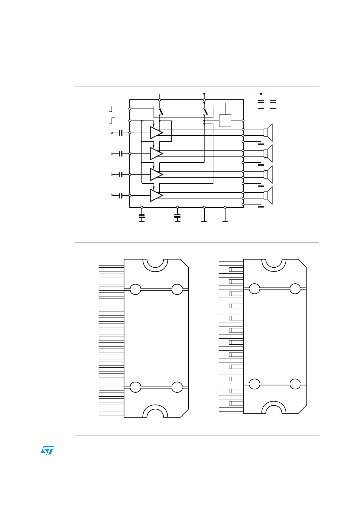
1 Block and pin connection diagram
Figure 1. Block diagram
Vcc1 Vcc2
ST-BY
MUTE
IN1
0.1μF
IN2
0.1μF
IN3
0.1μF
IN4
0.1μF
AC-GND
0.47μF47μF
SVR TAB S-GND
Figure 2. Pin connection (top view)
TAB
P-GND2
OUT2-
ST-BY
OUT2+
V
OUT1-
P-GND1
OUT1+
SVR
IN1
IN2
S-GND
IN4
IN3
AC-GND
OUT3+
P-GND3
OUT3-
V
OUT4+
MUTE
OUT4-
P-GND4
HSD
CC
CC
1
Flexiwatt25
vertical
25
D94AU159A
TAB
P-GND2
OUT2-
ST-BY
OUT2+
V
OUT1-
P-GND1
OUT1+
SVR
IN1
IN2
S-GND
IN4
IN3
AC-GND
OUT3+
P-GND3
OUT3-
V
OUT4+
MUTE
OUT4-
P-GND4
HSD
100nF470μF
HSD
CC
HSD/V
OUT1+
OUT1-
PW-GND
OUT2+
OUT2-
PW-GND
OUT3+
OUT3-
PW-GND
OUT4+
OUT4-
PW-GND
D94AU158D
1
OFF_DET
Flexiwatt25
horizontal
CC
25
D06AU1655
5/17
Electrical specifications TDA7560
2 Electrical specifications
2.1 Absolute maximum ratings
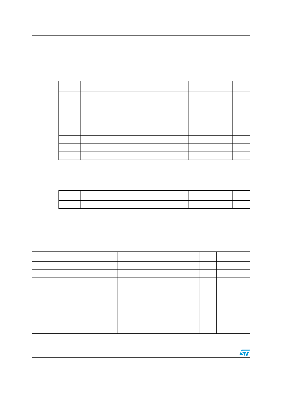
Table 2. Absolute maximum ratings
Symbol Parameter Value Unit
V
V
CC (DC)
V
CC (pk)
Operating supply voltage 18 V
CC
DC supply voltage 28 V
Peak supply voltage (for t = 50 ms) 50 V
Output peak current
I
Repetitive (duty cycle 10 % at f = 10 Hz)
O
Non repetitive (t = 100 µs)
P
T
Power dissipation T
tot
T
Junction temperature 150 °C
j
Storage temperature -55 to 150 °C
stg
= 70 °C 80 W
case
2.2 Thermal data
Table 3. Thermal data
Symbol Parameter Value Unit
R
th j-case
Thermal resistance junction to case Max. 1 °C/W
2.3 Electrical characteristics
10
9
A
A
Table 4. Electrical characteristics
(Refer to the test and application diagram, V
T
= 25 °C; unless otherwise specified).
amb
= 14.4 V; RL = 4 Ω; Rg = 600 Ω; f = 1 kHz;
S
Symbol Parameter Test condition Min. Typ. Max. Unit
I
Quiescent current RL = ∞ 80 200 320 mA
q1
V
dV
dG
Output offset voltage Play Mode ±50 mV
OS
During mute ON/OFF output
OS
offset voltage
Voltage gain 25 26 27 dB
G
v
Channel gain unbalance ±1 dB
v
V
P
Output power
o
= 13.2 V; THD = 10 %
S
= 13.2 V; THD = 1 %
V
S
VS = 14.4 V; THD = 10 %
= 14.4 V; THD = 1 %
V
S
23
16
28
20
25
19
30
23
±60 mV
6/17
W
 Loading...