

AM/FM car radio tuner IC with stereo decoder
Features
■ FM part
– AGC generation by RF and IF detection
– I/Q mixer for 1
rejection
–Mixer for 2
– Internal 450 kHz band pass filter with
bandwidth control by ISS
– Fully integrated FM demodulator with noise
cancellation
■ AM part
– Wide and narrow AGC generation
–Mixer for 1
conversion
–Mixer for 2
– Integrated AM-demodulator
– AM IF noise blanking
■ Stereo decoder
– PLL with adjustment free, fully integrated
VCO
– Automatic pilot dependent
MONO/STEREO switching
– Programmable ROLL-OFF compensation
– High cut and stereo blend-characteristics
programmable
– Dedicated RDS mute
– Audio noise blanker
■ Additional features
– VCO for world tuning range
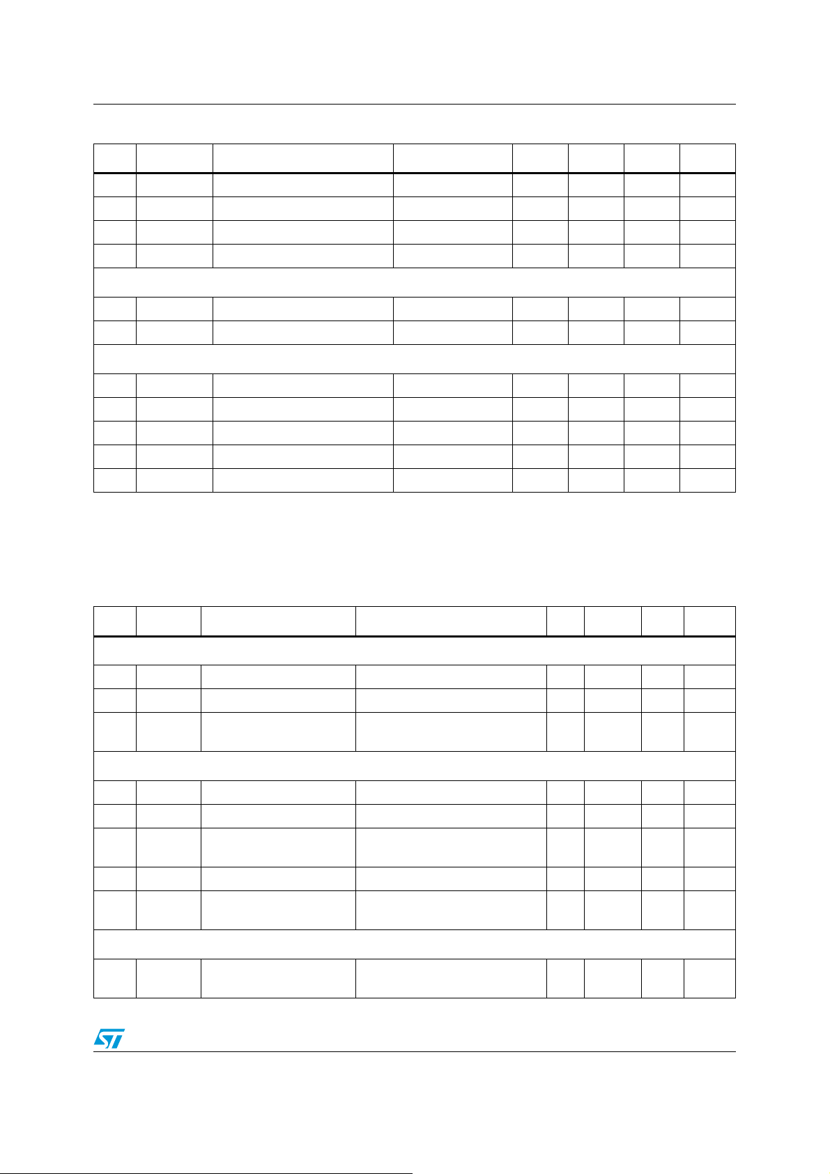
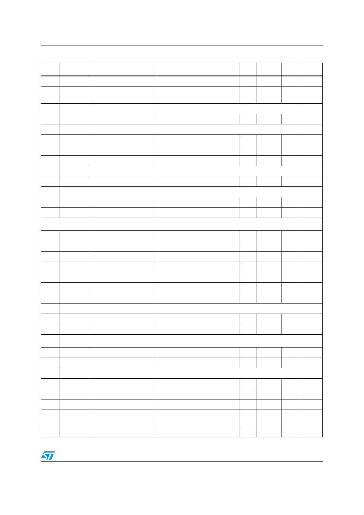
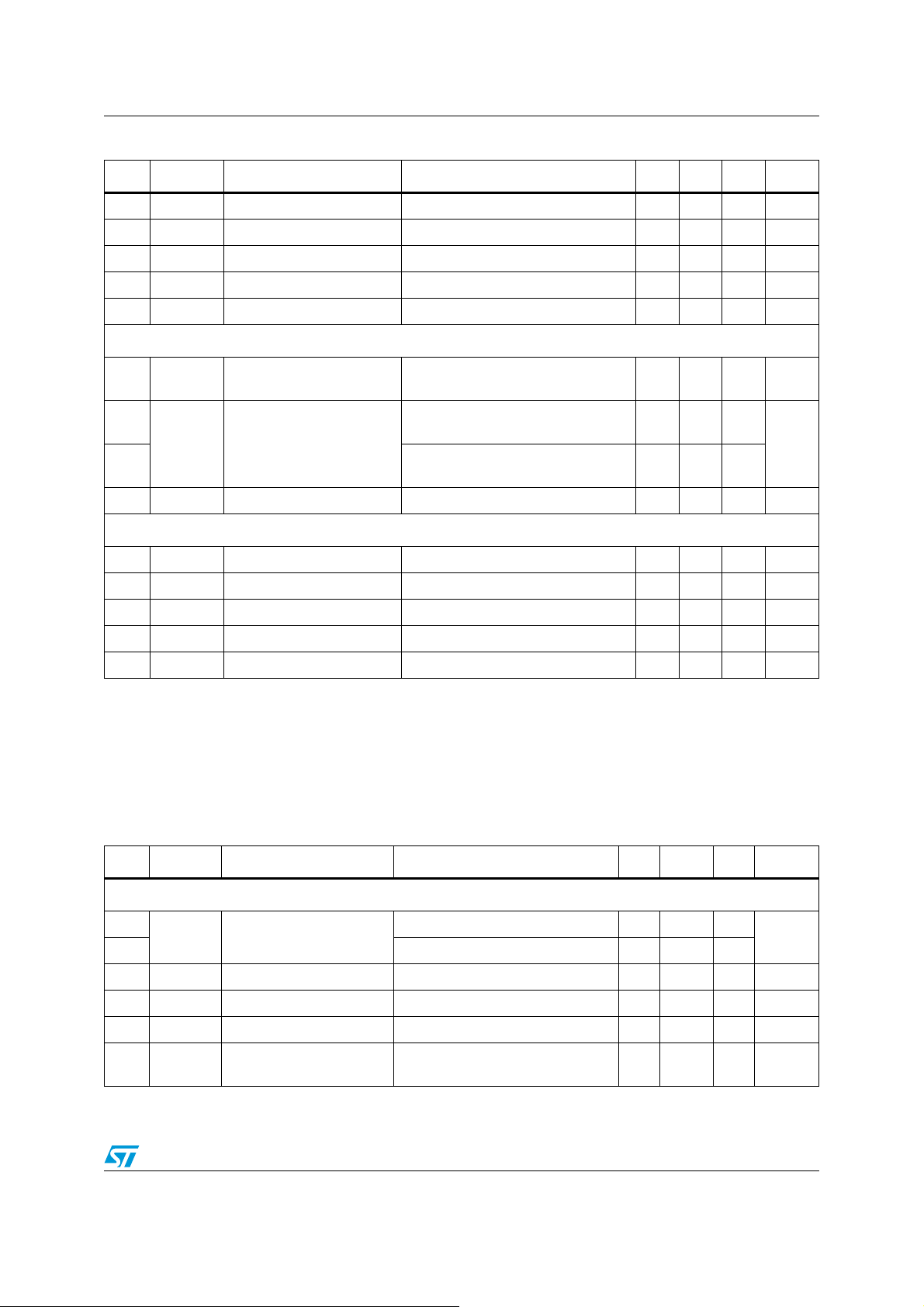
Table 1. Device summary
st
IF 10.7 MHz with image
nd
IF 450 kHz
st
IF 10.7 MHz, AM up
nd
IF 450 kHz
TDA7541B
and intelligent selectivity system
LQFP64
– High performance fast PLL for RDS-
System
– IF counter for FM and AM with search stop
signal
– Quality detector for level, deviation,
adjacent channel and multipath
– ISS (Intelligent selectivity system) for
cancellation of adjacent channel and noise
influences
– Adjacent channel mute
– Fully electronic alignment
– Independent weather band input
– All functions I
Description
The TDA7541B is a high performance tuner
circuit with stereo decoder for AM/FM car radio. It
contains a mixer, IF amplifier, demodulator for AM
and FM, stereo decoder, quality detection, ISS
filter and PLL synthesizer with IF counter on a
single chip. Use of BICMOS technology allows the
implementation of several tuning functions and a
minimum of external components.
2
C bus controlled
Order code Package Packing
TDA7541B LQFP64 (10 x 10 x 1.4 mm) Tray
TDA7541BTR LQFP64 (10 x 10 x 1.4 mm) Tape and reel
TDA7541BW LQFP64 (14 x 14 x 1.4 mm) Tray
TDA7541BWTR LQFP64 (14 x 14 x 1.4 mm) Tape and reel
July 2009 Doc ID 16048 Rev 1 1/77
www.st.com
1

Contents TDA7541B
Contents
1 Block circuit diagram . . . . . . . . . . . . . . . . . . . . . . . . . . . . . . . . . . . . . . . . 6
2 Pin connection and pin description . . . . . . . . . . . . . . . . . . . . . . . . . . . . 7
2.1 Pin connection . . . . . . . . . . . . . . . . . . . . . . . . . . . . . . . . . . . . . . . . . . . . . . 7
2.2 Pin description . . . . . . . . . . . . . . . . . . . . . . . . . . . . . . . . . . . . . . . . . . . . . . 8
3 Electrical specifications and characteristics . . . . . . . . . . . . . . . . . . . . 10
3.1 Thermal data . . . . . . . . . . . . . . . . . . . . . . . . . . . . . . . . . . . . . . . . . . . . . . 10
3.2 Absolute maximum ratings . . . . . . . . . . . . . . . . . . . . . . . . . . . . . . . . . . . . 10
3.3 Electrical characteristics . . . . . . . . . . . . . . . . . . . . . . . . . . . . . . . . . . . . . . 10
3.3.1 Globals . . . . . . . . . . . . . . . . . . . . . . . . . . . . . . . . . . . . . . . . . . . . . . . . . . 10
3.3.2 FM section . . . . . . . . . . . . . . . . . . . . . . . . . . . . . . . . . . . . . . . . . . . . . . . 11
3.3.3 AM section . . . . . . . . . . . . . . . . . . . . . . . . . . . . . . . . . . . . . . . . . . . . . . . 17
3.3.4 Stereo decoder section . . . . . . . . . . . . . . . . . . . . . . . . . . . . . . . . . . . . . 19
3.3.5 PLL section . . . . . . . . . . . . . . . . . . . . . . . . . . . . . . . . . . . . . . . . . . . . . . 24
4 Functional description . . . . . . . . . . . . . . . . . . . . . . . . . . . . . . . . . . . . . . 26
4.1 FM part . . . . . . . . . . . . . . . . . . . . . . . . . . . . . . . . . . . . . . . . . . . . . . . . . . . 26
4.1.1 Mixer 1 AGC and IF amplifier . . . . . . . . . . . . . . . . . . . . . . . . . . . . . . . . . 26
4.1.2 Mixer2, limiter, FM demodulator and spike cancellation . . . . . . . . . . . . 26
4.1.3 Quality detection and ISS . . . . . . . . . . . . . . . . . . . . . . . . . . . . . . . . . . . 26
4.1.4 Block diagram quality detection principle . . . . . . . . . . . . . . . . . . . . . . . . 29
4.1.5 Strong adjacent channel correction . . . . . . . . . . . . . . . . . . . . . . . . . . . . 30
4.1.6 Weak signal mute . . . . . . . . . . . . . . . . . . . . . . . . . . . . . . . . . . . . . . . . . 30
4.1.7 Weather band input . . . . . . . . . . . . . . . . . . . . . . . . . . . . . . . . . . . . . . . . 31
4.2 AM section . . . . . . . . . . . . . . . . . . . . . . . . . . . . . . . . . . . . . . . . . . . . . . . . 31
4.2.1 Usage of control bit ADSEL (Addr23D7) . . . . . . . . . . . . . . . . . . . . . . . . 32
4.3 Stereo decoder . . . . . . . . . . . . . . . . . . . . . . . . . . . . . . . . . . . . . . . . . . . . . 32
4.3.1 Decoder . . . . . . . . . . . . . . . . . . . . . . . . . . . . . . . . . . . . . . . . . . . . . . . . . 32
4.3.2 Noise blanker . . . . . . . . . . . . . . . . . . . . . . . . . . . . . . . . . . . . . . . . . . . . . 34
4.3.3 Functional description of the multipath detector . . . . . . . . . . . . . . . . . . 37
4.3.4 Quality detector . . . . . . . . . . . . . . . . . . . . . . . . . . . . . . . . . . . . . . . . . . . 37
4.3.5 AFS control and stereo decoder mute . . . . . . . . . . . . . . . . . . . . . . . . . . 37
4.4 PLL and IF counter section . . . . . . . . . . . . . . . . . . . . . . . . . . . . . . . . . . . 38
2/77 Doc ID 16048 Rev 1

TDA7541B Contents
4.4.1 PLL frequency synthesizer block . . . . . . . . . . . . . . . . . . . . . . . . . . . . . . 38
4.4.2 IF counter block . . . . . . . . . . . . . . . . . . . . . . . . . . . . . . . . . . . . . . . . . . . 39
4.5 I2C bus interface . . . . . . . . . . . . . . . . . . . . . . . . . . . . . . . . . . . . . . . . . . . . 39
5 Software specification . . . . . . . . . . . . . . . . . . . . . . . . . . . . . . . . . . . . . . 42
5.1 Chip address and overview . . . . . . . . . . . . . . . . . . . . . . . . . . . . . . . . . . . 42
5.2 Address organization . . . . . . . . . . . . . . . . . . . . . . . . . . . . . . . . . . . . . . . . 43
5.3 Control register function . . . . . . . . . . . . . . . . . . . . . . . . . . . . . . . . . . . . . . 44
5.4 Data byte specification . . . . . . . . . . . . . . . . . . . . . . . . . . . . . . . . . . . . . . . 47
6 Appendix . . . . . . . . . . . . . . . . . . . . . . . . . . . . . . . . . . . . . . . . . . . . . . . . . 68
7 Application circuit . . . . . . . . . . . . . . . . . . . . . . . . . . . . . . . . . . . . . . . . . . 74
8 Package information . . . . . . . . . . . . . . . . . . . . . . . . . . . . . . . . . . . . . . . . 75
9 Revision history . . . . . . . . . . . . . . . . . . . . . . . . . . . . . . . . . . . . . . . . . . . 76
Doc ID 16048 Rev 1 3/77

List of tables TDA7541B
List of tables
Table 1. Device summary . . . . . . . . . . . . . . . . . . . . . . . . . . . . . . . . . . . . . . . . . . . . . . . . . . . . . . . . . . 1
Table 2. Pin description . . . . . . . . . . . . . . . . . . . . . . . . . . . . . . . . . . . . . . . . . . . . . . . . . . . . . . . . . . . 8
Table 3. Thermal data. . . . . . . . . . . . . . . . . . . . . . . . . . . . . . . . . . . . . . . . . . . . . . . . . . . . . . . . . . . . 10
Table 4. Absolute maximum ratings . . . . . . . . . . . . . . . . . . . . . . . . . . . . . . . . . . . . . . . . . . . . . . . . . 10
Table 5. Globals . . . . . . . . . . . . . . . . . . . . . . . . . . . . . . . . . . . . . . . . . . . . . . . . . . . . . . . . . . . . . . . . 10
Table 6. FM section . . . . . . . . . . . . . . . . . . . . . . . . . . . . . . . . . . . . . . . . . . . . . . . . . . . . . . . . . . . . . 11
Table 7. AM section . . . . . . . . . . . . . . . . . . . . . . . . . . . . . . . . . . . . . . . . . . . . . . . . . . . . . . . . . . . . . 17
Table 8. Stereo decoder section . . . . . . . . . . . . . . . . . . . . . . . . . . . . . . . . . . . . . . . . . . . . . . . . . . . . 19
Table 9. PLL section . . . . . . . . . . . . . . . . . . . . . . . . . . . . . . . . . . . . . . . . . . . . . . . . . . . . . . . . . . . . . 24
Table 10. ISS filter control by I
Table 11. Internal ISS control signals . . . . . . . . . . . . . . . . . . . . . . . . . . . . . . . . . . . . . . . . . . . . . . . . . 29
Table 12. ISS control modes . . . . . . . . . . . . . . . . . . . . . . . . . . . . . . . . . . . . . . . . . . . . . . . . . . . . . . . 30
Table 13. Usage of ADSEL. . . . . . . . . . . . . . . . . . . . . . . . . . . . . . . . . . . . . . . . . . . . . . . . . . . . . . . . . 32
Table 14. Address organization . . . . . . . . . . . . . . . . . . . . . . . . . . . . . . . . . . . . . . . . . . . . . . . . . . . . . 43
Table 15. I
Table 16. Subaddress description . . . . . . . . . . . . . . . . . . . . . . . . . . . . . . . . . . . . . . . . . . . . . . . . . . . 47
Table 17. Addr 0 TPLL charge pump control (0Bh) . . . . . . . . . . . . . . . . . . . . . . . . . . . . . . . . . . . . . . 47
Table 18. Addr 1 TPLL Counter 1 (LSB). . . . . . . . . . . . . . . . . . . . . . . . . . . . . . . . . . . . . . . . . . . . . . . 48
Table 19. Addr 2 TPLL Counter 2 (MSB) . . . . . . . . . . . . . . . . . . . . . . . . . . . . . . . . . . . . . . . . . . . . . . 48
Table 20. Addr 3 TV(00h) . . . . . . . . . . . . . . . . . . . . . . . . . . . . . . . . . . . . . . . . . . . . . . . . . . . . . . . . . . 48
Table 21. Addr 4 TV/IF Counter (FM ACh, AM 1Ch) . . . . . . . . . . . . . . . . . . . . . . . . . . . . . . . . . . . . . 49
Table 22. Addr 5 TPLL Divider (FM 3Dh, AM 2Dh) . . . . . . . . . . . . . . . . . . . . . . . . . . . . . . . . . . . . . . 50
Table 23. Addr 6 AGC (FM 06h, AM 2Ah) . . . . . . . . . . . . . . . . . . . . . . . . . . . . . . . . . . . . . . . . . . . . . 51
Table 24. Addr 7 Quality AC (FM 50h) . . . . . . . . . . . . . . . . . . . . . . . . . . . . . . . . . . . . . . . . . . . . . . . . 52
Table 25. Addr 8 Quality ACM/MP (FM 6Ah) . . . . . . . . . . . . . . . . . . . . . . . . . . . . . . . . . . . . . . . . . . . 53
Table 26. Addr 9 Quality Dev (FM 49h) . . . . . . . . . . . . . . . . . . . . . . . . . . . . . . . . . . . . . . . . . . . . . . . 54
Table 27. Addr 10 Quality MUX/FSU (FM 0Eh, AM 0Fh) . . . . . . . . . . . . . . . . . . . . . . . . . . . . . . . . . . 55
Table 28. Addr 11 Weak Signal Mute (FM A8h) . . . . . . . . . . . . . . . . . . . . . . . . . . . . . . . . . . . . . . . . . 55
Table 29. Addr 12 AM IF NB (AM B1h) . . . . . . . . . . . . . . . . . . . . . . . . . . . . . . . . . . . . . . . . . . . . . . . 56
Table 30. Addr 13 XTAL adjust(80h) . . . . . . . . . . . . . . . . . . . . . . . . . . . . . . . . . . . . . . . . . . . . . . . . . 56
Table 31. Addr 14 IF2 adjust (FM E8h, AM 08h) . . . . . . . . . . . . . . . . . . . . . . . . . . . . . . . . . . . . . . . . 57
Table 32. Addr 15 IQ adjust / Switch (FM E7h) . . . . . . . . . . . . . . . . . . . . . . . . . . . . . . . . . . . . . . . . . 58
Table 33. Addr 16 FM keying AGC (FM 1Dh). . . . . . . . . . . . . . . . . . . . . . . . . . . . . . . . . . . . . . . . . . . 59
Table 34. Addr 17 Roll off / Level gain (77h) . . . . . . . . . . . . . . . . . . . . . . . . . . . . . . . . . . . . . . . . . . . 60
Table 35. Addr 18 SD Stereoblend / AM corner frequency (0Dh) . . . . . . . . . . . . . . . . . . . . . . . . . . . 61
Table 36. Addr 19 SD High cut (2Fh) . . . . . . . . . . . . . . . . . . . . . . . . . . . . . . . . . . . . . . . . . . . . . . . . . 62
Table 37. Addr 20 SD MP (FM 97h, AM 3Fh). . . . . . . . . . . . . . . . . . . . . . . . . . . . . . . . . . . . . . . . . . . 63
Table 38. Addr 21 SD Quality (FFM 7Ah, AM FAh) . . . . . . . . . . . . . . . . . . . . . . . . . . . . . . . . . . . . . . 64
Table 39. Addr 22 SD NB I (FM 05h, AM 04h) . . . . . . . . . . . . . . . . . . . . . . . . . . . . . . . . . . . . . . . . . . 65
Table 40. Addr 23 SD NB II (FM E2h, AM C2h) . . . . . . . . . . . . . . . . . . . . . . . . . . . . . . . . . . . . . . . . . 66
Table 41. Addr 24, 26, 27, 28, 29 testing (FEh) . . . . . . . . . . . . . . . . . . . . . . . . . . . . . . . . . . . . . . . . . 67
Table 42. Addr 25 Testing (FEh) . . . . . . . . . . . . . . . . . . . . . . . . . . . . . . . . . . . . . . . . . . . . . . . . . . . . 67
Table 43. Document revision history . . . . . . . . . . . . . . . . . . . . . . . . . . . . . . . . . . . . . . . . . . . . . . . . . 76
2
C control bit description . . . . . . . . . . . . . . . . . . . . . . . . . . . . . . . . . . . . . . . . . . . . . . . . . . 44
2
C bus. . . . . . . . . . . . . . . . . . . . . . . . . . . . . . . . . . . . . . . . . . . . . . . . . 28
4/77 Doc ID 16048 Rev 1

TDA7541B List of figures
List of figures
Figure 1. Block circuit diagram. . . . . . . . . . . . . . . . . . . . . . . . . . . . . . . . . . . . . . . . . . . . . . . . . . . . . . . 6
Figure 2. Pin connection (top view) . . . . . . . . . . . . . . . . . . . . . . . . . . . . . . . . . . . . . . . . . . . . . . . . . . . 7
Figure 3. Programming of HC filter . . . . . . . . . . . . . . . . . . . . . . . . . . . . . . . . . . . . . . . . . . . . . . . . . . 33
Figure 4. Programming of stereo blend . . . . . . . . . . . . . . . . . . . . . . . . . . . . . . . . . . . . . . . . . . . . . . . 34
Figure 5. Adaptive threshold control of noise blanker . . . . . . . . . . . . . . . . . . . . . . . . . . . . . . . . . . . . 35
Figure 6. Stereo blend controlled threshold adjust . . . . . . . . . . . . . . . . . . . . . . . . . . . . . . . . . . . . . . 36
Figure 7. Deviation controlled threshold adjust . . . . . . . . . . . . . . . . . . . . . . . . . . . . . . . . . . . . . . . . . 36
Figure 8. Block diagram FM part . . . . . . . . . . . . . . . . . . . . . . . . . . . . . . . . . . . . . . . . . . . . . . . . . . . . 68
Figure 9. Block diagram VCO . . . . . . . . . . . . . . . . . . . . . . . . . . . . . . . . . . . . . . . . . . . . . . . . . . . . . . 69
Figure 10. Block diagram ISS function. . . . . . . . . . . . . . . . . . . . . . . . . . . . . . . . . . . . . . . . . . . . . . . . . 70
Figure 11. Block diagram AM path. . . . . . . . . . . . . . . . . . . . . . . . . . . . . . . . . . . . . . . . . . . . . . . . . . . . 71
Figure 12. Block diagram stereo decoder . . . . . . . . . . . . . . . . . . . . . . . . . . . . . . . . . . . . . . . . . . . . . . 72
Figure 13. Block diagram audio noise blanker. . . . . . . . . . . . . . . . . . . . . . . . . . . . . . . . . . . . . . . . . . . 72
Figure 14. Block diagram multi path detection for stereo decoder. . . . . . . . . . . . . . . . . . . . . . . . . . . . 73
Figure 15. Application circuit . . . . . . . . . . . . . . . . . . . . . . . . . . . . . . . . . . . . . . . . . . . . . . . . . . . . . . . . 74
Figure 16. LQFP64 mechanical data and package dimensions . . . . . . . . . . . . . . . . . . . . . . . . . . . . . 75
Doc ID 16048 Rev 1 5/77
Block circuit diagram TDA7541B
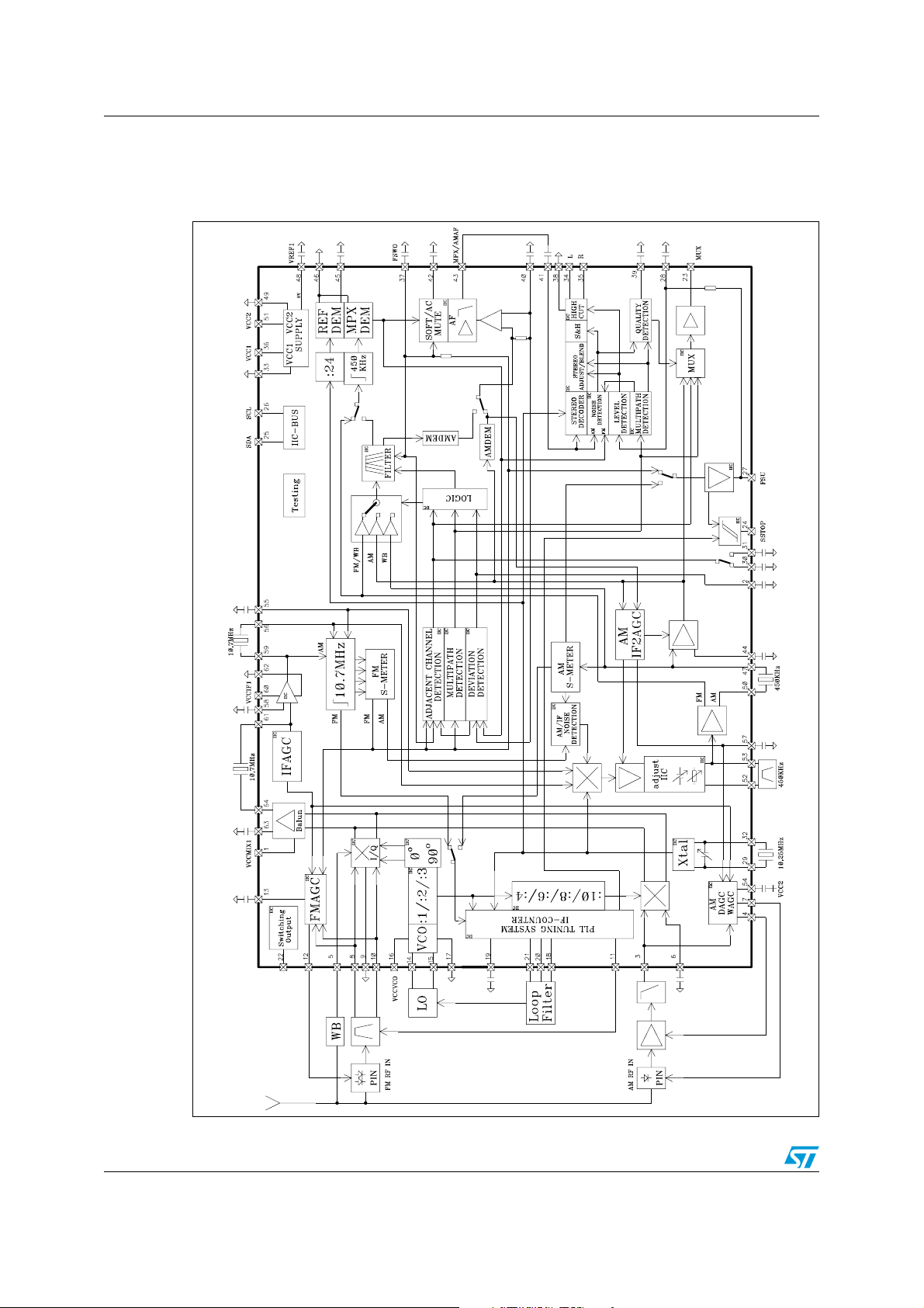
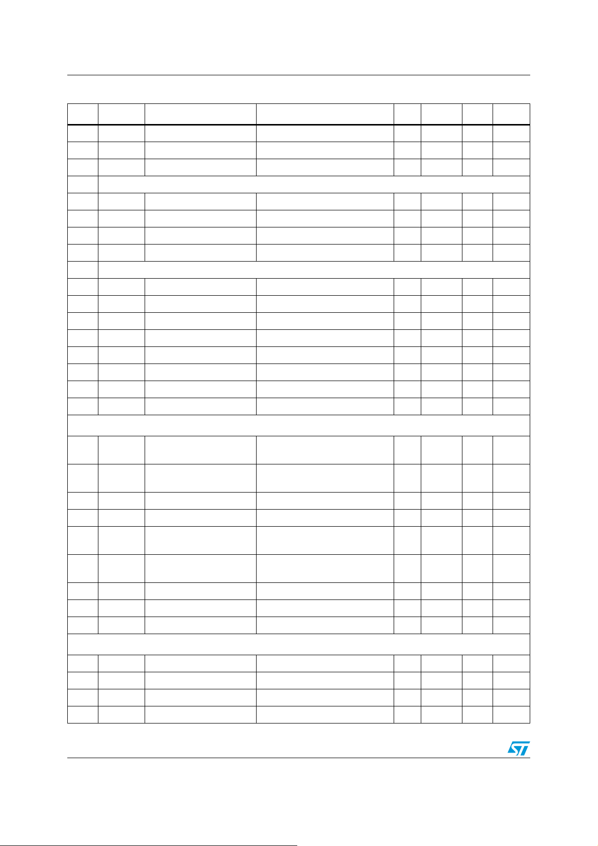
1 Block circuit diagram
Figure 1. Block circuit diagram
6/77 Doc ID 16048 Rev 1
TDA7541B Pin connection and pin description
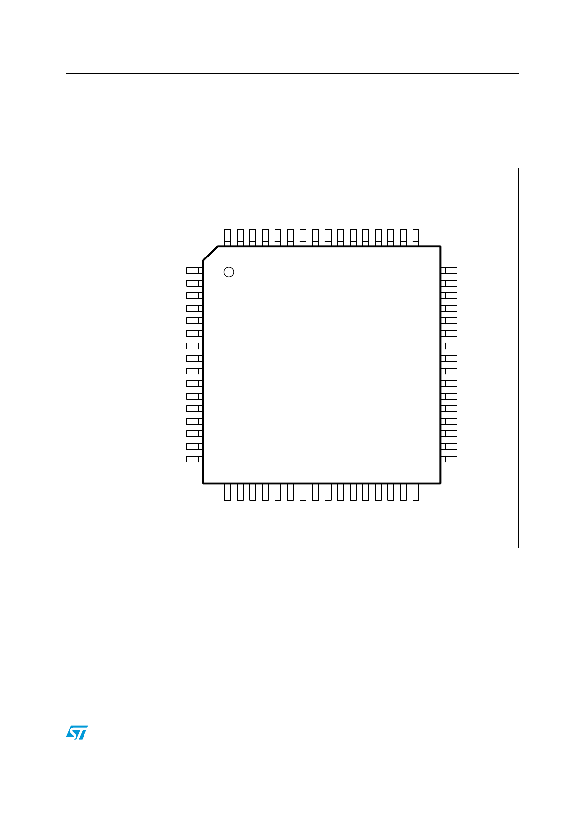
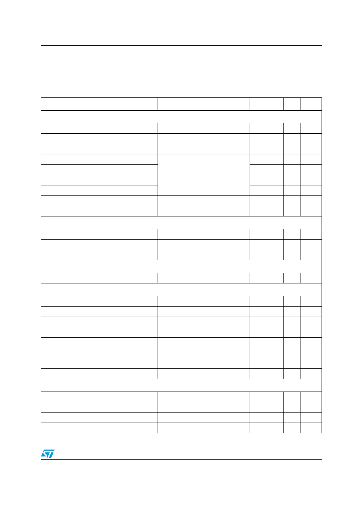
2 Pin connection and pin description
2.1 Pin connection
Figure 2. Pin connection (top view)
VCCMIX1
DEVTC
AMMIX1IN
AMRFAGCOUT
WB
AMMIX1RAF
AMPINDR
FMMIX1IN1
GNDRF
FMMIX1IN2
TV
FMPINDR
FMAGCTC
VCOB
VCOE
VCCVCO
1
2
3
4
5
6
7
8
9
10
11
12
13
14
15
16
MIX1OUT
63
64
18
17
GNDIF
MIX1REF
61
62
20
19
VCCIF1
IF1AMPIN
59
60
22
21
IF1REF
IF1AMPOUT
AMAGC2TC
58
57
24
23
AMRFAGCTC
MIX2IN56MIX2INREF
54
55
27
26
25
GNDVCC2
VCC2
MIX2REF
MIX2OUT53MIX2AMPOUT
49
51 50
52
48
47
46
45
44
43
42
41
40
39
38
37
36
35
34
33
32
31
30
29
28
VREF1
AMIF2IN
GNDDEM
FMREFDEMC
AMIF2REF
MPXOUT
MUTETC
MPXIN
AMREFDEMC
MPTC
GNDSTD
FSWO
VCC1
R
L
GNDVCC1
SW
LPF
VREF2
LPOUT
GNDVCO
LPHC
MUX
SDA
SSTOP
SCL
FSU
FSTC
XTALG
ISSTC1
XTALD
ISSTC2
Doc ID 16048 Rev 1 7/77

Pin connection and pin description TDA7541B
2.2 Pin description
Table 2. Pin description
Pin No. Pin name Function
1 VCCMIX1 Mixer1 Supply
2 DEVTC Deviation Detector Time Constant
3 AMMIX1IN AM Mixer1 Input
4 AMRFAGCOUT AM RF AGC Voltage Output
5 WB Weather Band Input
6 AMMIX1REF AM Mixer1 Reference
7 AMPINDR AM Pin Diode Driver Output
8 FMMIX1IN1 FM Mixer1 Input1
9 GNDRF RF Ground
10 FMMIX1IN2 FM Mixer1 Input2
11 TV Tuning Voltage Preselection
12 FMPINDR FM Pin Diode Driver Output
13 FMAGCTC FM AGC Time Constant
14 VCOB VCO Input Base
15 VCOE VCO Output Emitter
16 VCCVCO VCO Supply
17 GNDVCO VCO Ground
18 LPOUT OpAmp Output to PLL Loop Filter
19 VREF2 Voltage Reference for PLL OpAmp
20 LPF OpAmp Input to PLL Loop Filter
21 LPHC High Current PLL Loop Filter Input
22 SW Free Programmable Switch Output
23 MUX Multiplexer Output
24 SSTOP Search Stop Output
2
25 SDA I
26 SCL I
C Bus Data
2
C Bus Clock
27 FSU Unweighted Field Strength Output
28 FSTC S-meter Filtering Capacitor
29 XTALG Xtal Oscillator to MOS Gate
30 ISSTC1 ISS Filter Time Constant1 (slow)
31 ISSTC2 ISS Filter Time Constant2 (fast)
32 XTALD Xtal Oscillator to MOS Drain
33 GNDVCC1 Digital Ground
8/77 Doc ID 16048 Rev 1

TDA7541B Pin connection and pin description
Table 2. Pin description (continued)
Pin No. Pin name Function
34 L Stereo Decoder Output Left
35 R Stereo Decoder Output Right
36 VCC1 Digital Supply
37 FSWO Weighted Field Strength Output
38 GNDSTD Stereo Decoder Ground
39 MPTC Multipath Detector Time Constant
40 AMREFDEMC AM Demodulator Reference
41 MPXIN Stereo Decoder Input
42 MUTETC Weak Signal Mute Time Constant
43 MPXOUT AM Audio / MPX Output
44 AMIF2REF AM IF2 Amplifier Reference Voltage
45 FMREFDEMC FM Demodulator Reference
46 GNDDEM FM Demodulator Ground
47 AMIF2IN AM IF2 Amplifier Input
48 VREF1 5V Reference
49 GNDVCC2 Analog Ground
50 MIX2AMPOUT MIXER2 Amplifier Output
51 VCC2 Analog Supply
52 MIX2REF Mixer2 Reference
53 MIX2OUT Mixer2 Output
54 AMRFAGCTC AM RF AGC Time Constant
55 MIX2INREF Mixer2 Input Reference
56 MIX2IN Mixer2 Input
57 AMAGC2TC AM AGC2 Time Constant
58 IF1REF IF1 Amplifier Reference
59 IF1AMPOUT IF1 Amplifier Output
60 VCCIF1 IF1 Supply
61 IF1AMPIN IF1 Amplifier Input
62 GNDIF1 IF1 Ground
63 MIX1REF Mixer1 Reference
64 MIX1OUT Mixer1 Output
Doc ID 16048 Rev 1 9/77
Electrical specifications and characteristics TDA7541B
3 Electrical specifications and characteristics
3.1 Thermal data
Table 3. Thermal data
Symbol Parameter Value Unit
R
TH(j-amb)
Thermal resistance junction-to-ambient Max. 70 °C/W
3.2 Absolute maximum ratings
Table 4. Absolute maximum ratings
Symbol Parameter Conditions Value Unit
Supply voltage - 9.5 V
Ambient temperature - -40 to 85 °C
Storage temperature - -55 to +150 °C
ESD withstand voltage
T
V
V
amb
T
ESD
S
stg
3.3 Electrical characteristics
3.3.1 Globals
T
= 25 °C, V
amb
in application circuit, unless otherwise specified.
Table 5. Globals
CC1
= V
CC2
= V
CCMIX1
= V
Human Body Model 2 kV
Machine Model 100 V
Charged Device Model 300 V
CCVCO
= V
CCIF
= 8.5 V, f
= 10.25 MHz,
Xtal
Item Symbol Parameter Test conditions Min. Typ. Max. Unit
1. Supply
1.1 V
1.2 V
1.3 V
1.4 V
1.5 V
1.6 I
1.7 I
1.8 I
1.9 I
CC1
CC2
CCVCO
CCMIX1
CCIF
CC1
CC1
CC2
CC2
Digital supply voltage - 7.7 8.5 9 V
Analog supply voltage - 7.7 8.5 9 V
VCO supply voltage - 7.7 8.5 9 V
Mixer1 supply voltage - 7.7 8.5 9 V
IF1 Supply Voltage - 7.7 8.5 9 V
Supply current FM ON - 19 23 mA
Supply current AM ON - 21 25 mA
Supply current FM ON - 48 58 mA
Supply current AM ON - 37 44 mA
10/77 Doc ID 16048 Rev 1
TDA7541B Electrical specifications and characteristics
Table 5. Globals (continued)
Item Symbol Parameter Test conditions Min. Typ. Max. Unit
1.10 I
1.11 I
1.12 I
1.13 I
CCVCO
CCMIX1
CCMIX1
CCIF
Supply current - - 12 15 mA
Supply current FM ON - 32 40 mA
Supply current AM ON - 20 24 mA
Supply current - - 4 5 mA
2. Reference voltages
2.1 V
2.2 V
2
3. I
C bus interface
3.1 f
3.2 V
3.3 V
3.4 I
3.5 V
REF1
REF2
SCL
IL
IH
IN
O
Internal reference voltage I
Internal reference voltage I
Clock frequency - - - 400 kHz
Input low voltage - - - 1 V
Input high voltage - 2 - - V
Input current - -5 - 5 µA
Output acknowledge voltage IO = 1.6mA - - 0.4 V
3.3.2 FM section
T
= 25 °C, V
amb
f
= 98 MHz, dev = 40 kHz, f
RF
Table 6. FM section
CC1
= V
CC2
= 0mA 4.855.2V
REF1
= 0mA 2.4 2.5 2.6 V
REF2
= V
CCMIX1
Mod
= V
CCVCO
= V
CCIF
= 8.5 V, f
= 10.25 MHz,
Xtal
= 1 kHz, in application circuit, unless otherwise specified.
Item Symbol Parameter Test conditions Min. Typ. Max. Unit
4. Wide band RF AGC
4.1 V
4.2 V
4.3 Δ V
8-10
8-10
Lower threshold start V13 = 2.5 V, RFK “0” - 79 - dBμV
Upper threshold start V13 = 2.5 V, RFK”0” - 93 - dBμV
Control range RF KAGC
8-10
KAGC”000”, RFAGC”00”,
V
= 3.0….3.7 V, RFK”1”
37
5811-
5. Narrow band IF and keying AGC
5.1 V
5.2 V
5.3 V
5.4 V
5.5 Δ V
Lower threshold start KAGC = off, V
61
Upper threshold start KAGC = off, V
61
Max. IFAGC threshold
61
with KAGC
Start point KAGC KAGC”000”,IFAGC”00”, 3.2 3.4 3.6 V
37
Control range IF KAGC
61
KAGC”000”,IFAGC”00”,
V37 = 3.0 V
KAGC”000”,IFAGC”00”,
= 3.2….3.9 V
V
37
8-10
8-10
= 0 mV
= 0 mV
RMS
RMS
- 82 - dBµV
- 94 - dBµV
- 97 - dBµV
12 15 18 dB
6. AGC time constant output
V
6.1 V
Max. AGC output voltage V
13
8-10
= 0 mV
RMS
--
REF1
+V
BE
V
Doc ID 16048 Rev 1 11/77
Electrical specifications and characteristics TDA7541B
Table 6. FM section (continued)
Item Symbol Parameter Test conditions Min. Typ. Max. Unit
6.2 V
6.3 I
6.4 I
Min. AGC output voltage V
13
Min. AGC charge current V
13
Max. AGC discharge
13
current
V
8-10
8-10
8-10
= 100 mV
= 0 mV
RMS,V13
= 100 mV
RMS
--0.5V
= 2.5 V -33 -25 -17.5 µA
RMS,V13
= 2.5 V 1.7 2.5 3.3 mA
7. AGC PIN diode driver output
7.1 I
7.2 I
AGC OUT, current min. V
12
AGC OUT, current max. V
12
8-10
8-10
= 0 mV
= 50 mV
, V12 = 2.5V 15 25 35 µA
RMS
, V12 = 2.5 V - - -16 mA
RMS
8. FM I/Q Mixer1 (10.7 MHz)
8.1 R
8.2 C
8.3 R
8.4 V
OUT
8,11
Input resistance Differential 8 10 12 kΩ
IN
Input capacitance Differential - 4 - pF
IN
Output resistance - 530 660 790 Ω
Input DC bias - 2.2 2.5 2.8 V
8.5 G Gain Unloaded 20 22 24 dB
8.6 G
Gain With 330 Ω load 14 16 18 dB
l
8.7 INOISE Equivalent input noise - - 3 - nV/
8.8 CP
8.9 IIP3 3
1dB compression point Referred to diff. mixer input - 100 - dBµV
1dB
rd
order intermodulation - - 119 - dBµV
√Hz
8.10 IQP I/Q phase adjust PH -7 - +8 DEG
8.11 IRR Image rejection ratio Ratio wanted/image 30 40 - dB
8.12 IRR Image rejection ratio With phase adjust 40 46 - dB
9. WB I/Q Mixer1 (10.7 MHz)
9.1 R
9.2 C
9.3 R
9.4 V
OUT
Input resistance Single ended 1.7 2.5 3.3 kΩ
IN
Input capacitance Single ended - 3 - kΩ
IN
Output resistance - 530 660 790 Ω
Input dc bias - 2 2.3 2.6 V
5
9.5 G Gain unloaded 24 26 28 dB
9.6 INOISE Equivalent Input noise Source impedance 400 Ω -2.3 -nV/
9.7 IIP3 3
rd
order intermodulation - - 113 - dBµV
√Hz
10. IF1 amplifier (10.7 MHz)
10.1 R
10.2 C
10.3 V
10.4 R
10.5 C
OUT
OUT
Input resistance - 265 330 396 Ω
IN
Input capacitance - - 2.5 - pF
IN
DC input voltage - - V
61
/3 - V
CCIF1
Output resistance - 265 330 396 Ω
Output capacitance - - 2.5 - pF
12/77 Doc ID 16048 Rev 1
TDA7541B Electrical specifications and characteristics
Table 6. FM section (continued)
Item Symbol Parameter Test conditions Min. Typ. Max. Unit
10.6 V
10.7 G
10.8 G
10.9 INOISE
10.10 CP
10.11 IIP3 3
DC output voltage - - V
59
Min. gain IFG - 9 - dB
min
Max. gain IFG - 21 - dB
max
, R
Equivalent input noise
voltage
1 dB compression point referred to 330 Ω input, G
1dB
rd
order Intermodulation referred to 330 Ω input, G
G
max
noise of R
=330 Ω, RL=330 Ω,
gen
not included
gen
max
max
CCIF1
- 3.2 - nV/√Hz
-99 -dBµV
- 130 - dBµV
/2 - V
11. Mixer2 (450kHz)
11.1 R
11.2 C
11.3 V
11.4 R
11.5 C
11.6 V
11.7 g
55.56
OUT
OUT
52,53
Input resistance Differential 240 300 360 Ω
IN
Input capacitance - - 2.5 - pF
IN
DC input voltage - 3.7 4
Output resistance - 100 - - kΩ
Output capacitance - - 2.5 - pF
DC output voltage - 3.7 4 4.3 V
Conversion
m
transconductance
WB Mode; referred to MIX2OUT - 126 - µA/V
4.3 V
11.8 G Gain FM Mode, referred to MIX2OUT - 16 - dB
11.9 C
11.10 C
step
max
11.11 INOISE
11.12 CP
11.13 IIP3 3
Min. cap. Step IF2A - 2.2 - pF
Max. cap. IF2A - 33 - pF
Equivalent input noise
voltage,
including buffer mixer2
1dB compression point referred to 330 Ω input,IF2Q”10” - 116 - dBμV
1dB
rd
order Intermodulation referred to 330 Ω input,IF2Q”10” - 132 - dBμV
= 330 Ω, IF2Q”10”
R
gen
noise of R
gen
not included
-15 -nV/√Hz
12. Demodulator, audio output
12.1 THD Total harmonic distortion
12.2 a
12.3 V
12.4 R
12.5 R
MPX
OUT
LOAD
AM suppression
AM
MPX output signal Dev.= 75 kHz 440 500 560 mV
Output impedance - 20 40 60 Ω
Load resistance - 10 - - kΩ
Dev.= 75 kHz, V
IF2Q”11”
V
=100 dBµ, Δf = 40 KHz,
56
f
=1 kHz,
mod
=1 kHz@AM, m =0.3 %
f
mod
= 100 dBµV,
56
- 0.1 0.3 %
40 60 - dB
RMS
Doc ID 16048 Rev 1 13/77
Electrical specifications and characteristics TDA7541B
Table 6. FM section (continued)
Item Symbol Parameter Test conditions Min. Typ. Max. Unit
12.6 (S+N)/N
Signal plus noise-to-noise
ratio at MPXOUT
Signal plus noise-to-noise
12.7 (S+N)/N
ratio
In weatherband mode
13. Quality detection
Unweighted field strength (FSU) and weighted field strength
13.1 V
13.2 V
13.3 V
13.4 V
13.5 ΔV
13.6 ΔV
13.7 R
13.8 V
OUT
DC output voltage
37
DC output voltage
37
DC output voltage
37
DC output voltage
37
Slope - - 25 - mV/dB
37
DC offset - -200 - 0 mV
37
Output impedance FSWO 17 23.5 30 kΩ
DC output voltage
27
Δf = 40 kHz, f
=100 dBµV,
V
56
mod
=1 kHz,
De-emphasis = 50 µs,
B = 200 Hz to 15 kHz
ISSENA = 0
Δf = 3.5 kHz, f
V
=100 dBµV,
56
mod
=1 kHz,
De-emphasis = 75 µs,
setting see Ta bl e 1 0
= 20 dBμV, FMON=1,
V
56
FSWO = OFF
= 50 dBμV, FMON=1,
V
56
FSWO = OFF
V
= 70 dBμV, FMON=1,
56
FSWO = OFF
> 120 dBμV, FMON=1,
V
56
FSWO = OFF
= 20 dBμV, FMON=1,
V
56
SL=”101”
70 - - dB
40 - - dB
-2.5 - V
-3 -V
-3.5 - V
-4.6 - V
-0.10.4V
V
= 50 dBμV, FMON=1,
13.9 V
13.10 V
13.11 V
13.12 ΔV
13.13 R
13.14 R
13.15 V
13.16 V
13.17 V
13.18 V
27
27
27
27
OUT
load
27
27
27
27
DC output voltage
DC output voltage
DC output voltage
Slope - - 50 - mV/dB
Output impedance FSU 320 400 480 Ω
Load resistor FSU - 20 - kΩ
DC output voltage AM
DC output voltage AM
DC output voltage AM
DC output voltage AM
56
SL=”101”
= 70 dBμV, FMON=1,
V
56
SL=”101”
> 120 dBμV, FMON=1,
V
56
SL=”101”
V
= 20 dBμV, FMON = 0,
47
SL= ”010”
= 40 dBμV, FMON = 0,
V
47
SL= ”010”
= 60 dBμV, FMON = 0,
V
47
SL= ”010”
V
> 100 dBμV, FMON = 0,
47
SL= ”010”
14/77 Doc ID 16048 Rev 1
-1 -V
-2 -V
4- -V
-0.10.3V
-1.25 - V
-3.0 - V
4.5 - - V
TDA7541B Electrical specifications and characteristics
Table 6. FM section (continued)
Item Symbol Parameter Test conditions Min. Typ. Max. Unit
13.19 ΔV
13.20 f
Slope AM FMON=0 - 90 - mV/dB
27
-3 dB frequency low pass
LP
AM
FMON=0 - 40 - kHz
Adjacent channel gain
13.21 G
Gain - - 32 - dB
AC
Adjacent channel filter
13.22 f
13.23 f
13.24 f
HP
-20dB
BP
-3 dB frequency highpass ACF=0 - 100 - kHz
Attenuation 20dB - - 70 - kHz
Centre frequency ACF=1 - 100 - kHz
Multipath channel gain
13.25 G
Gain - - 12 - dB
MP
Multipath bandpass filter
13.26 f
Centre frequency - - 19 - kHz
C
13.27 Q Quality factor - 5 8 10 -
14. ISS (intelligent selectivity system) filter 450kHz
14.1 f
centre
Centre frequency f
REF_intern
= 450kHz 450 kHz
14.2 BW 3dB Bandwidth, -3 dB ISSBW = 1 70 80 90 kHz
14.3 BW 20dB Bandwidth, -20 dB ISSBW = 1 132 150 168 kHz
14.4 BW 3dB Bandwidth, -3 dB ISSBW = 0 106 120 135 kHz
14.5 BW 20dB Bandwidth, -20 dB ISSBW = 0 220 250 280 kHz
14.6 BW 3dB Bandwidth weather band WBON = 1 18 22 26 kHz
14.7 BW 20dB -20dB weather band WBON = 1 - 70 - kHz
Adjacent channel ISS filter threshold
14.8 V
14.9 V
THAC
THAC
Internal low threshold ACTH - 2.75 - V
Internal high threshold ACTH - 3.05 - V
Multipath threshold
14.10 V
14.11 V
THMP
THMP
Internal low threshold MPTH - 0.50 - V
Internal high threshold MPTH - 1.25 - V
ISS filter time constant
14.12 I
14.13 I
14.14 I
14.15 I
14.16 I
30,31
30,31
30,31
30,31
30,31
Charge current low mid TISS, BWDEF = 1 -89 -74 -59 µA
Charge current high mid TISS, BWDEF = 1 -72 -60 -48 µA
Charge current low narrow TISS, BWDEF = 1 -148 -124 -99 µA
Charge current high
narrow
TISS, BWDEF = 1 -132 -110 -88 µA
Discharge current low TISS, BWDEF = 0 0.5 1 1.5 µA
Doc ID 16048 Rev 1 15/77
Electrical specifications and characteristics TDA7541B
Table 6. FM section (continued)
Item Symbol Parameter Test conditions Min. Typ. Max. Unit
14.17 I
14.18 V
14.19 V
30,31
30,31
30,31
Discharge current high TISS, BWDEF = 0 11 15 19 µA
Low voltage BWDEF = 0 - 0.1 0.2 V
High voltage BWDEF = 1 4.6 4.9 - V
ISS filter switch threshold
14.20 V
14.21 V
14.22 V
14.23 V
30,31
30,31
30,31
30,31
Threshold ISS on BWDEF = 0 - 3 - V
Threshold ISS off BWDEF = 0 - 1 - V
Threshold ISS narrow on BWDEF = 0 - 4 - V
Threshold ISS narrow off BWDEF = 0 - 2 - V
Deviation detection
14.24 I
14.25 I
14.26 I
14.27 I
14.28 DEV
14.29 DEV
14.30 RATIO
14.31 RATIO
Charge current low TDEV -40 -32 -20 µA
3
Charge current high TDEV -48 -39 -30 µA
3
Discharge current low TDEV 0.5 1 1.5 µA
3
Discharge current high TDEV 5.5 8 10.5 µA
3
Internal low threshold DWTH, I3 = 1 µA - 20 - kHz
WTH
Internal high threshold DWTH, I3 = 1 µA - 50 - kHz
WTH
Referred to threshold DTH - 1 -
min
Referred to threshold DTH - 1.5 -
max
15. Weak signal mute
15.1 V
15.2 V
15.3 a
15.4 a
15.5 a
15.6 V
MTHISS
ACMTH
15.7 a
15.8 I
15.9 I
WMD
WMD
ACMD
Upper start point
37
Lower start point
37
Min. mute depth WMD = 0, WMTH = 7, V
Max. mute depth WMD = 7, WMTH = 7, V56=OFF 22 26 - dB
Mute threshold below
WMTH for ISS filter “ON”
Internal AC mute
threshold
AC mute depth ACMD 3 - 8 dB
Charge current - -65 -47.5 -30 μA
42
Discharge current - 1.5 2.5 4 μA
42
16. Multiplexer output
16.1 V
16.2 V
16.3 R
16.4 R
OUT
23load
Output voltage low - - 0.1 0.2 V
23
Output voltage high - 4.6 4.9 - V
23
Output resistance - 200 250 300 Ω
Load resistor - 20 - - kΩ
WMTH = 0, WMD = 7, V
AF = -3 dB
WMTH = 7, WMD = 7, V
AF = -3 dB
WMD, WMTH, V
IN=V56
,
IN=V56
IN=V56
=OFF 10 14 - dB
56
-2.9 - V
,
-2.7 - V
-1 -dB
ACMTH 40 - 260 mV
16/77 Doc ID 16048 Rev 1
TDA7541B Electrical specifications and characteristics
3.3.3 AM section
T
= 25 °C, V
amb
f
= 1 MHz, m = 30%, f
RF
Table 7. AM section
Item Symbol Parameter Test conditions Min. Typ. Max. Unit
17. Global
17.1 V
ANT_US
Usable sensitivity
17.2 (S+N)/N Signal to Noise Ratio Ref.: V
17.3 a
17.4 V
17.5 V
17.6 V
17.7 V
17.8 V
17.9 V
IF1 rejection S/N = 26 dB, m = 30 %, f
IF
Min. RF AGC threshold
3
Max. RF AGC threshold - 104 - dBµV
3
Min. IF AGC threshold
61
Max. IF AGC threshold - 102 - dBµV
61
Min. DAGC threshold
56
Max. DAGC threshold - 98 - dBµV
56
18. AGC voltage driver output
CC1
= V
(1)
= V
CC2
mod
CCMIX1
= 1 kHz, in application circuit, unless otherwise specified.
= V
CCVCO
= V
CCIF
= 8.5 V, f
= 10.25 MHz,
Xtal
(S+N)/N = 26 dB - 19 25 dBµV
= 80 dBµV 50 55 - dB
3
= 1 kHz 70 80 - dB
mod
- 92 - dBµV
RFAGC
- 78 - dBµV
IFAGC
- 86 - dBµV
DAGC
18.1 V
18.2 V
18.3 | I
Max. AGC output voltage - 3.3 3.5 - V
4
Min. AGC output voltage - - - 0.5 V
4
AGC current V4 = 0 V, V54 = 3.5 V, LNA”00” - 340 - µA
4 |
19. AGC PIN diode driver output
19.1 I
AGC driver current - - - -15 mA
7
20. AM Mixer1 (10.7 MHz)
20.1 R
20.2 C
20.3 R
OUT
20.4 CP
20.5 V
20.6 IIP3 3
20.7 INOISE Equivalent input noise - - 5.5 -
Input resistance differential 45 - - kΩ
IN
Input capacitance differential - 2.5 - pF
IN
Output impedance - 530 660 790 Ω
1dB compression point referred to diff. mixer input - 112 - dBμV
1dB
Input DC bias - 0.3 0.4 0.55 V
3,6
rd
order intermodulation - - 132 - dBμV
nV/√Hz
20.8 G Gain With 330 Ω filter 35.57 dB
21. AM mixer2
21.1 R
21.2 C
21.3 V
21.4 R
55.56
OUT
Input resistance - 240 300 360 Ω
IN
Input capacitance - - 2.5 - pF
IN
DC input voltage - 3.8 4 4.2 V
Output resistance - 100 - - kΩ
Doc ID 16048 Rev 1 17/77
Electrical specifications and characteristics TDA7541B
Table 7. AM section (continued)
Item Symbol Parameter Test conditions Min. Typ. Max. Unit
21.5 C
21.6 V
21.7 g
21.8 G
OUT
52,53
max
Output capacitance - - 2.5 - pF
DC output voltage - 3.7 4.0 4.3 V
Conversion
m
transconductance
Max. gain
MIX2OUT - 440 - µA/V
L = 560 µH, Q = 28; C = 180 pF,
referred to MIX2OUT
-26- dB
21.9 ΔG Gain control range - - 20 - dB
21.10 C
21.11 C
step
max
21.12 INOISE
21.13 CP
21.14 IIP3 3
Min. cap. Step IF2A - 2.2 - pF
Max. cap. IF2A - 33 - pF
Equivalent input noise
voltage,
including buffer mixer2
1dB compression point A
1dB
rd
order Intermodulation A
, R
A
max
of R
max
max
= 330 Ω, RL = 2 kΩ, noise
gen
not included
gen
-11-
, referred to 330 Ω input -114-dBμV
, referred to 330 Ω input -132-dBμV
nV/√H
22. Buffer AM mixer2
22.1 R
22.2 C
OUT
OUT
22.3 V
22.4 G gain R
Output resistance - 1.6 2 2.4 kΩ
Output capacitance - - 2.5 - pF
DC output voltage - 3.7 4.0 4.3 V
50
= 2 kΩ -8 -6 -4 dB
L
23. AM IF2 amplifier
z
23.1 R
23.2 C
23.3 V
23.4 G
23.5
IN
IN
44,47
max
ΔG Gain control range - 36 38 40 dB
23.6 INOISE
23.7 CP
1dB
23.8 IIP3 3
23.9 V
23
24. AMAGC2
24.1 V
24.2
24.3 g
AGC(start)
ΔAGC AGC2 range
AGC
Input resistance - 1.6 2 2.4 kΩ
Input capacitance - - 2.5 - pF
DC input voltage - 4.1 4.3 4.5 V
Max. gain - 495255 dB
, R
Equivalent input noise
voltage
1 dB compression point G
rd
order Intermodulation G
G
max
noise of R
max
max
IF2 output voltage V56 = 90 dBV, m = off 140 190 240
= 2 kΩ,
gen
gen
not included
-9.5-
nV/√Hz
, referred to 2 kΩ input -74-dBμV
, referred to 2 kΩ input -100-dBμV
mV
RMS
AGC start voltage (PIN47) Input carrier voltage - 62 - dBµV
Between start of AGC2
and the intervention point
50 55 - dB
of prestage AGC
Control slope Seek mode - 50 - µA/V
18/77 Doc ID 16048 Rev 1
TDA7541B Electrical specifications and characteristics
Table 7. AM section (continued)
Item Symbol Parameter Test conditions Min. Typ. Max. Unit
24.4 g
24.5 II
24.6 II
24.7 V
24.8 V
AGC
57
57
Control slope normal mode - 5 - µA/V
I Max. AGC charge current Seek mode - 125 - μA
I Max. AGC charge current normal mode - 5 - μA
Max. AGC output voltage V47 = 100 dBµ 4.6 4.8 - V
57
Min. AGC output voltage V47 = 20 dBµ - 0.2 0.5 V
57
25. AM audio output
25.1 V
Audio output voltage
43
25.2
THD Total harmonic distortion
25.3
25.4 R
OUT
Output impedance - 20 25 30 Ω
26. IF noise blanking
26.1 t
26.2 t
26.3 V
26.4 V
26.5 V
1. Can be reached in application circuit, not measured.
thstep
Min. blanking time - - 8 - μs
bl
Max. blanking time - - 17 - μs
bl
Min internal threshold - - 50 - mV
th
Max. internal threshold - -
th
Threshold step - - 12.5 - mV
= 90 dBµ, m = 30 %,
V
56
f
= 1KHz
mod
V
= 90 dBµ, m = 30 %,
56
f
= 1 kHz
mod
= 90 dBµ, m = 80%,
V
56
= 1 kHz
f
mod
170 200 230
-0.30.5
-0.50.9
187.5
-mV
mV
RM
S
%
3.3.4 Stereo decoder section
T
= 25 °C, V
amb
V
= 500 mV
MPX
otherwise specified.
Table 8. Stereo decoder section
Item Symbol Parameter Test conditions Min. Typ. Max. Unit
27. Stereo decoder
27.1
27.2 WBON = 1 - 0.05 0.06
27.3 R
27.4 G
27.5 G
27.6 SVRR
V
in
in
STD
STDWB
MPX input level
Input resistance - 80 100 120 kΩ
Stereo decoder gain - 2 2.5 3 dB
Stereo decoder gain Weather band mode 23 26 27 dB
Supply voltage ripple
rejection
= V
CC1
mono, f = 1 kHz, de-emphasis τ = 50 µs, in application circuit, unless
rms
CC2
= V
CCMIX1
= V
CCVCO
= V
CCIF
= 8.5 V, f
= 10.25 MHz,
Xtal
--0.50.93
V
= 100 mV, f = 1 kHz - 60 - dB
ripple
Doc ID 16048 Rev 1 19/77
V
rms

Electrical specifications and characteristics TDA7541B
Table 8. Stereo decoder section (continued)
Item Symbol Parameter Test conditions Min. Typ. Max. Unit
27.7 A channel separation
= 500 mV
V
MPX
L/R, ROC adjusted
stereo, only
rms
35 40 - dB
27.8 THD Total harmonic distortion - - 0.02 0.3 %
27.9 (S+N)/N
Signal plus noise to noise
ratio
A-weighted, 19 kHz notch - 85 - dB
28. Mono/stereo switch
28.1 V
28.2 V
28.3 V
28.4 V
PTHST1
PTHST0
PTHMO1
PTHMO0
Pilot threshold voltage for Stereo, PTH = 1 5 8 12 mV
Pilot threshold voltage for Stereo, PTH = 0 7 11 16 mV
Pilot threshold voltage for Mono, PTH = 1 3.5 6 10 mV
Pilot threshold voltage for Mono, PTH = 0 6 9 14 mV
29. 19kHz PLL
29.1 f
lock
29.2 DP Pilot deviation range f
Capture range Pilot magnitude 20 mV
= 19 kHz 4 - 30 %
pilot
= 4 % 18.9 - 19.1 kHz
rms
30. De-emphasis and high cut
30.1 t
30.2 t
HC50
HC75
De-emphasis time
constant
De-emphasis time
constant
DEEMP=0, High Cut OFF 45 50 55 μs
DEEMP = 1, High Cut OFF 67 75 83 μs
rms
rms
rms
rms
30.3 t
30.4 t
30.5 A
30.6 A
HC50
HC75
Ammin
Ammax
High cut time constant
High cut time constant
Min. Attenuation in AM
Max. Attenuation in AM
31. Stereo blend and high cut control
31.1 LG
31.2 LG
31.3 LG
31.4 VSBL
31.5 VSBL
31.6 VSBL
31.7 VHCH
31.8 VHCH
Min. level gain LG -0.3 0 0.3 dB
min
Max. level gain LG 7.75 8.25 8.75 dB
max
Level gain step Resolution - 0.25 0.55 0.85 dB
step
Min. voltage for mono SBC 24 29 34 %V
min
Max. voltage for mono SBC 53 58 63 %V
max
Step resolution SBC 3.5 4.2 5 %V
step
Min. voltage for no high
min
cut
Max.voltage for no high
max
cut
DEEMP = 0, High Cut ON,
V
=0.1V
28
DEEMP= 1, High Cut ON,
= 0.1 V
V
28
Voutmax/Vout@ f = 3.5 kHz,
DEEMP = 0, AMCF “111”
Voutmax/Vout@ f = 3.5 kHz,
DEEMP= 0, AMCF “000”
HCHT 374247%V
HCHT 616671%V
135 150 165 μs
200 225 250 μs
-3.6- dB
-8-dB
REF1
REF1
REF1
REF1
REF1
20/77 Doc ID 16048 Rev 1
TDA7541B Electrical specifications and characteristics
Table 8. Stereo decoder section (continued)
Item Symbol Parameter Test conditions Min. Typ. Max. Unit
31.9 VHCH
31.10 VHCL
31.11 VHCL
31.12 VHCL
Step resolution HCHT 7 8 9 %V
step
Min. voltage for full high cut
min
Max. voltage for full high cut
max
Step resolution HCLT 6.5 7.3 8.1 %VHCH
step
HCLT 6 11 16 %VHCH
HCLT 28 33 38 %VHCH
32. Carrier and harmonic suppression at the output
32.1 a19 Pilot signal f = 19 kHz - 45 50 - dB
32.2 a38 Subcarrier f = 38 kHz - - 75 - dB
32.3 a57 Subcarrier f = 57 kHz - - 62 - dB
32.4 a76 Subcarrier f = 76 kHz - - 90 - dB
mod
mod
(2)
(1)
= 10 kHz, f
= 13 kHz, f
=1 kHz - - 65 - dB
spur
=1 kHz - - 75 - dB
spur
33. Intermodulation
33.1 a2 f
33.2 a3 f
34. Traffic radio
34.1 a57 Signal f = 57 kHz - 65 70 - dB
35. SCA
(3)
35.1 a67 Signal f = 67 kHz - - 75 - dB
36. ACI – adjacent channel interference
(4)
REF1
36.1 a114 Signal f = 114 kHz - - 95 - dB
36.2 a190 Signal f = 190 kHz - - 84 - dB
37. FM noise blanker
37.1 V
37.2 V
37.3 V
37.4 V
37.5 V
37.6 V
37.7 V
37.8 V
37.9 V
TRMIN
TRMAX
TRNOISE
TRNOISE
PEAK
PEAK
PEAK
PEAKDEV
PEAKDEV
Min. trigger threshold
Max. trigger threshold
Min. noise controlled
trigger threshold
Max. noise controlled
trigger threshold
Peak voltage NBRR “00”, V
Peak voltage
Peak voltage
Min. deviation dependent
peak voltage
Max. deviation dependent
peak voltage
(5)
V
PEAK
(5)
V
PEAK
V
PEAK
V
PEAK
NBRR “00”, V
f = 150 kHz
NBRR “00”, V
f = 150 kHz
V
MPX
NBDC = 11 (“OFF”)
V
MPX
=0.8 V, NBLT “111” - 147 - mV
=0.8 V, NBLT “000” - 280 - mV
= 1.5 V, NBCT “11” - 450 - mV
= 1.5 V, NBCT “00” - 1200 - mV
= 0 mV - 0.8 - V
MPX
= 50 mV,
MPX
MPX
= 500 mV,
= 200 mV,
-1.9- V
-3.5- V
-0.8- V
= 500 mV, NBDC= 00 - 2.0 - V
OP
OP
OP
OP
Doc ID 16048 Rev 1 21/77
Electrical specifications and characteristics TDA7541B
Table 8. Stereo decoder section (continued)
Item Symbol Parameter Test conditions Min. Typ. Max. Unit
37.10 V
37.11 V
PEAKFS
PEAKFS
37.12 T
37.13 T
37.14 SR
37.15 SR
37.16 V
37.17 V
37.18 V
37.19 V
37.20 V
37.21 V
37.22 V
RECTADJ
RECTADJ
RECTADJ
RECTADJ
ADJMP
ADJMP
ADJMP
Min. fieldstrength
controlled peak voltage
Max. fieldstrength
controlled peak voltage
Min. blanking time
S
Max. blanking time
S
Noise rectifier charge
PEAK
Noise rectifier charge
PEAK
Noise rectifier discharge
adjustment
Noise rectifier discharge
adjustment
Noise rectifier discharge
adjustment
Noise rectifier discharge
adjustment
Noise rectifier adjustment
by multipath
Noise rectifier adjustment
by strong multipath
influence
Noise rectifier adjustment
by multipath and strong
multipath influence
V
MPX
=0mV, V
LEVEL
<< V
SBL
(fully mono), NBFC = 11 (“OFF”)
V
MPX
=0mV, V
LEVEL
<< V
SBL
(fully mono), NBFC = 00
Signal HOLDN in testmode,
NBT = 00
Signal HOLDN in testmode,
NBT = 11
Signal PEAK in testmode,
NBPC =0
Signal PEAK in testmode,
NBPC=1
Signal PEAK in testmode,
NBRR=00
Signal PEAK in testmode,
NBRR=01
Signal PEAK in testmode,
NBRR=10
Signal PEAK in testmode,
NBRR=11
Signal PEAK in testmode,
=1V, NBSMP=0, NBMP=1,
V
MPTC
NBRR=01
Signal PEAK in testmode,
V
= 1V, NBSMP = 1,
MPTC
NBMP = 0, NBRR = 01
Signal PEAK in testmode,
=1 V, MBSMP=1,
V
MPTC
NBMP=1, NBRR=01
-0.8- V
-2.0- V
-38- μs
-22- μs
-5-mV/μs
-12-mV/μs
- 0.3 - V/ms
- 1.8 - V/ms
- 2.8 - V/ms
-4-V/ms
-3-V/ms
-4-V/ms
- 5.2 - V/ms
38. Multipath detector
38.1 G
38.2 G
38.3 G
38.4 G
RECTMP
RECTMP
38.5 I
38.6 I
38.7 I
DISMP
CHMP
CHMP
Min. multipath gain MPG = 00 5 6 7 dB
MP
Max. multipath gain MPG = 11 11 12 13 dB
MP
Min. rectifier gain MPRG = 01 -1 0 1 dB
Max. rectifier gain MPRG = 11 5 7.6 9 dB
Rectifier charge current MPCC = 0 0.5 0.8 1.1 μA
Rectifier charge current MPCC = 1 0.2 0.4 0.7 μA
Rectifier discharge current 0.5 1 - mA
39. Quality detector
39.1 a
Min. quality detector
coefficient
QDC 0.5 0.6 0.7 -
22/77 Doc ID 16048 Rev 1

TDA7541B Electrical specifications and characteristics
Table 8. Stereo decoder section (continued)
Item Symbol Parameter Test conditions Min. Typ. Max. Unit
39.2 a
Max. quality detector
coefficient
QDC 0.9 1.05 1.2 -
39.3 b Min. quality noise gain QNG 5 6 7 dB
39.4 b Max. quality noise gain QNG 13 15 17 dB
1. Intermodulation suppression
V
signal @1 kHz,()
o
---------------------------------------------------------------
a2
V
spurious @1 kHz,()
o
V
signal @1 kHz,()
o
---------------------------------------------------------------
a3
V
spurious @1 kHz,()
o
measured with: 91 % stereo signal; 9 % pilot signal; fm = 10 kHz or 13 kHz.
2. Traffic radio (V.F.) suppression
a57 V W F,,()
------------------------------------------------------------------------------------------=
V
measured with: 91% stereo signal; 9% pilot signal; fm=1 kHz; 5% sub carrier (f=57 kHz, fm=23 Hz AM, m=60 %)
3. SCA (subsidiary communications authorization)
signal @1 kHz,()
V
o
---------------------------------------------------------------
a67
V
spurious @9 kHz,()
o
measured with: 81 % mono signal; 9 % pilot signal; fm=1 kHz; 10 % SCA - sub carrier (f
ƒs 2 10 kHz×()19 kH z–()=;=
ƒs 3 13 kHz×()38 kH z–()=;=
signal @1 kHz,()
V
o
spurious @1 kHz,()23 k H z±
o
ƒs 2 38 kHz×()67 kH z–()=;=
= 67 kHz, unmodulated)
S
4. ACI (adjacent channel interference)
signal @1 kHz,()
V
o
---------------------------------------------------------------
a114
V
spurious @4 kHz,()
o
signal @1 kHz,()
V
o
---------------------------------------------------------------
a190
V
spurious @4 kHz,()
o
measured with: 90 % mono signal; 9 % pilot signal; fm=1 kHz; 1% spurious signal (f
5. All thresholds are measured in test mode at the quality output. The thresholds are calculated by V
be adjusted by applying a 150 kHz sinewave at MPXIN.
ƒs 110 k Hz 2 38 kHz×()–()=;=
ƒs 186 k H z 5 38 k Hz×()–()=;=
= 110 kHz or 186 kHz, unmodulated)
S
NBTH
- V
PEAK
. V
PEAK
can
Doc ID 16048 Rev 1 23/77
Electrical specifications and characteristics TDA7541B
3.3.5 PLL section
T
V
amb
MPX
= 25 °C, V
= 500 mV
= V
CC1
mono, f = 1 kHz, de-emphasis τ = 50 µs, in application circuit, unless
rms
CC2
= V
CCMIX1
= V
CCVCO
= V
CCIF
= 8.5 V, f
= 10.25 MHz,
Xtal
otherwise specified.
Table 9. PLL section
Item Symbol Parameter Test conditions Min. Typ. Max. Unit
40. Voltage controlled oscillator (VCO)
40.1 f
40.2 f
VCOmin
VCOmax
40.3 C/N Carrier-to-noise-ratio
Min. VCO frequency - 160 - - MHz
Max. VCO frequency - - - 260 MHz
f
= 200 MHz, Δf=1 kHz,
VCO
B = 1 Hz, Q
loaded
=60
-80-dBc/
√Hz
41. Crystal oscillator
41.1 f
41.2 C/N Carrier-to-noise-ratio f
41.3 V
41.4 C
29-32
41.5 C
41.6 C
41.7 Δf/f Deviation versus V
Crystal frequency - - 10.25 - MHz
xtal
=10.25 MHz, Δf=10 kHz 110 - - dBc/√Hz
xtal
Oscillator output voltage - - 400 - mV
29
Input capacitance - - 2.5 - pF
Min. cap. Step XTAL - 0.75 - pF
step
Max. cap. XTAL - 23.25 - pF
max
CC
Δ VCC=1 V - 1.5 - ppm/V
rms
41.8 Δf/f Deviation versus T -40 °C<T<+85 °C - 0.2 - ppm/K
42. Charge pump current
42.1 -I
42.2 I
42.3 -I
42.4 I
42.5 -I
42.6 I
42.7 -I
42.8 I
Source current
20
Sink current - 50 - μA
20
Source current
20
Sink current - 500 - μA
20
Source current
20
Sink current - 1 - mA
20
Source current - 1.9 - mA
20
Sink current - 1.9 - mA
20
= 2.5 V
V
20
ICP, V
ICP, V
= 2.5 V
20
= 2.5 V
20
-50- μA
-550- μA
-1- mA
43. Loop filter input/output
43.1 -I
43.2 I
43.3 V
43.4 V
43.5 I
43.6 I
IN
IN
OL
OH
OUT
OUT
Input leakage current VIN = GND: PD
Input leakage current VIN = VREF1 PD
Output voltage Low I
Output voltage High I
Output current, sink V
Output current, source V
= -0.2 mA - 0.05 0.5 V
OUT
= 0.2 mA
OUT
= 1 V to V
OUT
= 1 V to V
OUT
= Tristate -0.1 - 0.1 μA
OUT
OUT
CCVCO
CCVCO
24/77 Doc ID 16048 Rev 1
= Tristate -0.1 - 0.1 μA
V
-
V
CCVCO
0.5
CCVCO
0.05
-
-V
-1 V - - 10 mA
-1 V -10 - - mA

TDA7541B Electrical specifications and characteristics
Table 9. PLL section (continued)
Item Symbol Parameter Test conditions Min. Typ. Max. Unit
44. Output of tuning voltage (TV)
-
V
44.1 V
44.2 IV
44.3 IV
44.4
44.5 R
44.6 R
ΔV Additional offset voltage TVM=1, TVO+ - 3.175 - V
Output voltage - 0.5 -
OUT
I Min. voltage step TVO - 25 - mV
step
I Max. voltage offset TVO - 3175 - mV
max
Output impedance TVM=0 - 40 - kΩ
OUT
Output impedance TVM=1 - 20 - kΩ
OUT
45. SSTOP output (open collector)
VCO
0.5
V
45.1 V
45.2 V
45.3 -I
45.4 I
45.5 V
45.6 V
24
24
24
24
37SSTH
27SSTH
46. Switch output
46.1 V
46.2 V
46.3 -I
46.4 I
46.5 V
46.6 V
46.7 I
OL
OH
22
22
OL
OH
22
Output voltage low I24 = -200 μA -0.20.5 V
Output voltage high - - - 5 V
Output leakage current V 24 = 5 V -0.1 - 0.1 μA
Output current, sink V 24 = 0.5 V to 5 V - 1 mA
Internal unfiltered field
strength threshold for
SSTH, FMON=1 2.6 - 4.1 V
SSTOP=HIGH
Internal unfiltered field
strength threshold for
SSTOP=HIGH
SSTH, FMON=0
SL = “011”
1.2 - 4.8 V
Output Voltage low SWM”1”,SW”0”, I24 = -5 µA - 0.35 0.5 V
Output Voltage high SWM”1”,SW”1” - VCC-1 - V
Output leakage current V22=5 V -0.5 - 0.5 μA
Output Current, sink - - - 7 mA
Output Voltage low SWM”0”,SW”0”, I22=0 µA - 0.1 0.3 V
Output Voltage high SWM”0”,SW”1”, I22=1 mA - VCC-1 - V
Output Current, sink V22=5 V -7 - - mA
Doc ID 16048 Rev 1 25/77

Functional description TDA7541B
4 Functional description
4.1 FM part
4.1.1 Mixer 1 AGC and IF amplifier
FM quadrate I/Q-mixer converts FM RF to IF1 of 10.7 MHz. The mixer provides inherent
image rejection and wide dynamic range with low noise and large input signal performance.
For accurate image rejection the phase-error of I/Q can be compensated by software (PH).
It is capable of tuning the US FM, US weather (dedicated WB input), Europe FM, Japan FM
and East Europe FM bands:
– US FM = 87.9 to 107.9 MHz
– US weather = 162.4 to 162.55 MHz
– Europe FM = 87.5 to 108 MHz
– Japan FM = 76 to 91 MHz
– East Europe FM = 65.8 to 74 MHz
The AGC operates on different sensitivities and bandwidths in order to improve the input
sensitivity and dynamic range. AGC thresholds are programmable by software (RFAGC,
IFAGC, and KAGC). The output signal is a controlled current for pin diode attenuator.
A 10.7 MHz programmable amplifier (IFG) correct the IF ceramic insertion loss and the
costumer level plan application.
4.1.2 Mixer2, limiter, FM demodulator and spike cancellation
In the 2nd mixer stage the first 10.7 MHz IF is converted into the second 450 kHz IF.
The fully integrated sample and hold FM demodulator including spike cancellation (DSB)
converts the IF signal from the 450 kHz limiter (limiter gain 80 dB typ.) to the FM multiplex
output signal with very low distortion.
The sensitivity of spike blanking can be set via I
2
C bus.
4.1.3 Quality detection and ISS
Field strength
Parallel to mixer2 input a 10.7 MHz limiter generates a signal for digital IF counter and field
strength voltage V
adjacent channel and multi path detection and is available at PIN27 (FSU) in a range of 0 V
to 5 V. The offset and slope of FSU signal can be adjusted via I
application adaptation.
The voltage VFSWO including offset adjust is externally filtered at PIN37 (FSWO) and used
for weak signal mute function and generation of ISS filter control signals in weak signal
condition. It is possible to combine the IF counter result with this voltage VFSWO by
programmable comparator threshold (SSTH).
. This internal voltage V
FSUint
is used for AM IF noise blanker,
FSUint
2
C bus (FSWO and SL) for
26/77 Doc ID 16048 Rev 1

TDA7541B Functional description
Adjacent channel detector
The input of the adjacent channel detector is AC coupled from VFSW. A programmable
high-pass or band-pass (ACF) as well as rectifier generate a signal which is compared with
adjustable threshold (ACTH). The output signals of this comparator is controlling the charge
and discharge of the external capacitor at PIN30 or PIN31 (dependent on SEEK) with
programmable discharge current (TISS). The level at PIN30/31 is used to generate the two
digital signal ac and ac+ for ISS control. The adjacent channel information behind the
rectifier is available as analog output signal at the multiplexer output (PIN23).
Multipath detector
The input of the multi path detector is AC coupled from internal VFSW too. After filtering with
19 kHz band-pass and rectifying, this voltage is compared with an adjustable threshold
(MPTH). The output signal of this comparator can be used to switch off the adjacent channel
detection. This influence is selectable by I
The multi path information behind the rectifier is available as analog output signal at
multiplexer output (PIN23).
2
C bus (MPENA).
450 kHz IF narrow band pass filter (ISS filter)
The device has an additional 450 kHz IF narrow band-pass filter for suppression of noise
and adjacent channel signal influences. This narrow filter has three switchable bandwidths,
narrow range of 80 kHz, mid range of 120 kHz and 22 kHz for weather band information.
Without ISS (Intelligent Selectivity System) filter the IF bandwidth (wide range) is defined
only by ceramic filter chain and mixer2 bandwidth. The filter is located between mixer2
output buffer and 450 kHz limiter stage. The centre frequency is matched to the
demodulator centre frequency.
Deviation detector
In order to avoid distortion in audio output signal the narrow ISS filter is switched OFF if over
deviation is present. Hence the demodulator output signal is detected. After AC coupling,
low-pass filtering and peak rectifying this signal is charging/discharging the external DEVTC
capacitor by an IIC programmable charge/discharge current (TDEV). The voltage at DEVTC
is compared with adjustable thresholds (DWTH, DTH) and generates two digital control
signals (dev, dev+). For weak signal condition the deviation threshold depends on FSWO.
ISS switch logic
All digital control signals coming from adjacent channel detector, deviation detector and
weak signal mute are acting via switching matrix on ISS filter switch. IF2 narrow band-pass
switch mode is controlled also by software (ISSENA, ISSON, WBON, ISSBW, and BWDEF).
The switching of the IF band-pass is also possible to influence by external manipulation of
DC voltage at PIN30.
The influence of the ISS software control on the functionality of the ISS filter is described in
Ta bl e 1 0 . The value “X” for the control bit means the bit does not influence the filter control in
this condition.
Doc ID 16048 Rev 1 27/77

Functional description TDA7541B
Table 10. ISS filter control by I
I2C control bits
ISSENA adr4/d2
ISSON adr11/d0
ISSBW adr7/d0
WBON adr11/d1
ISSM adr9/d7
BWDEF adr7/d1
0XXXXXISS filter is switched off (bypass)
1 1 0 X X X ISS filter is in manual control mode, Band width is 120 kHz
1 1 1 X X X ISS filter is in manual control mode, Band width is 80 kHz
11X1XX
10XX00
10XX10
100X01
100X11
101X01
101X11
ISS filter is in manual control mode, Band width is 22 kHz
This setting must be used for weather band application
ISS filter is in automatic control mode
Filter activation and band width defined by control table mode1
ISS filter is in automatic control mode
Filter activation and band width defined by control table mode2
ISS filter is in automatic control mode
Filter activation defined by control table mode1
band width fixed to 120 kHz
ISS filter is in automatic control mode
Filter activation defined by control table mode2
band width fixed to 120 kHz
ISS filter is in automatic control mode
Filter activation defined by control table mode1
band width fixed to 80 kHz
ISS filter is in automatic control mode
Filter activation defined by control table mode2
band width fixed to 80 kHz
2
C bus
Notes
Description of I2C bits:
ISSENA
ISS filter enable
“1”: ISS filter control enabled
“0”: ISS filter is switched off (bypass of the filter, wide)
ISSON
ISS filter control mode
“1”: ISS filter is in manual control mode (switched "ON"); the bits ISSBW and WBON are
defining the bandwidth
“0”: ISS filter is in automatic control mode according to mode1/2 table
ISSBW
ISS filter band width
“1”: 80 kHz
28/77 Doc ID 16048 Rev 1

TDA7541B Functional description
“0”: 120 kHz
The bit has only influence if bit BWENA is “1”, or if bit ISSON is “1”
WBON
Weather band enable
“1”: Weather band enable (FMmixer1 is disabled, Wbmixer1enabled, stereo decoder gain
26dB, ISS filter bandwidth 22 kHz, IF2Q=”00”)
“0”: Weather band disable
For weather band enable it is need to set ISSON = “1”
ISSM
ISS filter application mode
“0”: ISS filter application mode1
“1”: ISS filter application mode2
If BWENA is “1” the band width is always switched to ISSBW in case of ISS filter activated
BWDEF
Enable bit ISSBW for ISS filter band with control
“1”: ISS filter is internally controlled, but band width is defined by bit ISSBW
“0”: ISS filter is internally controlled, band width is defined by mode1/2 table
For the internal control two application modes are available (ISSM). The conditions and
settings are described in Ta bl e 1 1 and Tab le 1 2.
4.1.4 Block diagram quality detection principle
(without overdeviation correction)
Table 11. Internal ISS control signals
Signal Low High
Ac No adjacent channel Adjacent channel present
ac+ No strong adjacent channel Adjacent channel higher as ac
Sm
Dev Deviation lower as threshold DWTH Deviation higher as threshold DWTH
dev+ Deviation lower as threshold DTH*DWTH Deviation higher as threshold DTH*DWTH
Inton ISS filter off by logic (wide) ISS filter on by logic
int80 ISS filter 120 kHz (mid) ISS filter 80 kHz (narrow)
Field strength higher as weak signal mute
threshold
Field strength lower as weak signal mute
threshold
Doc ID 16048 Rev 1 29/77

Functional description TDA7541B
Table 12. ISS control modes
Input signals Mode1 Mode2
ac ac+ sm dev dev+ inton int80 Function inton int80 Function
0000000wide0 0wide
0001000wide0 0wide
0001100wide0 0wide
0010011narrow1 1narrow
0011000wide1 0 mid
0011100wide0 0wide
1000011narrow1 0 mid
1100011narrow1 1narrow
1001010mid1 0 mid
1101110mid1 1narrow
4.1.5 Strong adjacent channel correction
Under strong adjacent channel it is possible to have disturbance of the audio signal created
by interference between ISS filter control (deviation detection) and adjacent channel mute.
The control bits SACCE and SACCT can be used to avoid this disturbance. If the function is
activated (SACCE = “1”) the IF counter together with the internal field strength is used to
suppress a malfunction of deviation detection. The bit SACCT is changing the sensitivity of
the SACC block (SACCT = “1” means higher sensitivity).
Figure 10 shows the ISS block diagram including the SACC function.
Note: The IF counter must be switched ON if this function is used (Addr25D4 = “1”)
4.1.6 Weak signal mute
The filtered field strength signal (FSWO) is the reference for soft slope mute control in weak
signal condition to eliminate audible effects. The start point and mute depth are
programmable (WMTH, WMD) in a wide range. These settings together with FSWO bits are
influencing the weak signal mute behavior. The time constant is defined by external
capacitance at PIN 42. Additional adjacent channel mute function is supported. A high pass
filter with -3 dB threshold frequency of 100 kHz, amplifier and peak rectifier generates an
adjacent noise signal from Demodulator output. This value is compared with adjustable
threshold (ACMTH). For present strong adjacent channel the MPX signal is additional
attenuated (ACMD) and has the same time constant as weak signal mute.
30/77 Doc ID 16048 Rev 1

TDA7541B Functional description
4.1.7 Weather band input
If the weather band input is used the chip must be set in FM mode (FMON). In addition to
that the ISS filter must be switched ON (ISSENA=”1”), mixer2 quality factor must be set to
IF2Q=”00” and the ISS filter must be set in manual control mode (ISSON=”1”).
The bit WBON is:
● activating the WB input
● switching the ISS filter in WB mode (22 kHz band width)
● switching the stereo decoder InGain to 26 dB.
In order to increase the selectivity in weather band mode the AM 450kHz ceramic filter can
be used in series to the ISS filter by activating ADSEL (please refer to Figure 10, ISS block
diagram and Section 4.2.1, usage of bit ADSEL).
4.2 AM section
signals, narrow band information (DAGC) referred to PIN 56, up conversion signal (IFAGC)
at PIN 61 and wide band information (RFAGC) at PIN 3.This gain control gives two output
signals. The first one is a current for pin diode attenuator and the second one is a voltage for
preamplifier. Time constant of RF and IF-AGC is defined by internal 100 kΩ resistor and
external capacitor at PIN 54. The intervention points for AGC (DAGC, IFAGC and RFAGC)
are programmable by software. The oscillator frequency for upconversion-mixer1 is
generated by dividing the VCO frequency after VCO divider (VCOD) and AM pre-divider
(AMD).
Two 10.7 MHz ceramic filters before mixer2 input increase 900 kHz attenuation.
The AMIF2 block contains mixer2, IF2 amplifier, demodulator and AGC2 The AM/FM mixer2
converts 10.7 MHz IF1 into 450 kHz IF2. Mixer2 output passes a 450 kHz narrow band filter
(LC plus ceramic filter). LC centre frequency is adjustable by I
2
C bus (IF2A). The following
IF2 amplifier provides signal for fully integrated demodulator. If the bit ADSEL is activated,
the ISS filter is inserted between IF2 amplifier and demodulator in order to increase the
selectivity (please refer to Figure 11, AM path block diagram and Section 4.2.1, usage of bit
ADSEL).
Mixer2 and IF2 amplifier have a 2-stage AGC with careful take-over behavior to keep
distortion low. The IF2 AGC range is about 55 dB.
The input signal of IF2 amplifier is used in limiter circuit for in-band level detection. The
electrical characteristics are described in FM section.
The demodulator is a peak detector to generate the audio output signal.
At the MUX output the AMIF stereo is available.
AM IF noise blanker
In order to remove in AM short spikes a noise cancellation conception is used in 450 kHz IF
AM level. The advantage is to avoid long narrow AGC- and demodulator- time constants,
which enlarge spike influences on audio signal and makes difficult to remove it in audio path.
The 10.7 MHz AM IF signal behind IF1 amplifier generates via limitation an unweighted field
strength signal including slope of noise spike. The comparison of this detected slope
between fast and slow rectifier ignores audio modulation whereby the threshold of slow
Doc ID 16048 Rev 1 31/77

Functional description TDA7541B
rectifier is programmable (AINBT). A comparator activates a pulse generator. The duration
of this pulse is software programmable (AINT) and is smooth blanking out the spikes in mixer2.
4.2.1 Usage of control bit ADSEL (Addr23D7)
The control bit ADSEL can be used to increase the selectivity of the application in AM mode
and WB mode. In FM it has no function. Table 12 shows the functionality of the control bit.
Table 13. Usage of ADSEL
FMON WBON ADSEL
Note
Addr4D7 Addr11D1 Addr23D7
1 0 X Standard FM mode
Weather band mode using 450 kHz ceramic filter;
ISS filter must be manually switched on in order to limit the band
11 0
11 1
0 0 0 Standard AM mode
00 1
width at 450 kHz IF (ISSENA/ISSON = "1");
450 kHz ceramic filter is switched in series to ISS filter to
increase selectivity
Standard weather band mode;
ISS filter must be manually switched on in order to limit the band
width at 450 kHz IF (ISSENA/ISSON = "1")
AM mode using ISS filter;
ISS filter (22 kHz band width) is switched in series to the 450 kHz
ceramic filter
01 XNot allowed
4.3 Stereo decoder
4.3.1 Decoder
The stereo decoder-part of the TDA7541B contains all functions necessary to demodulate
the MPX-signal, like pilot tone-dependent MONO/STEREO switching as well as the stereo
blend and high cut.
Adaptations like programmable input gain, roll-off compensation, selectable de-emphasis
time constant and a programmable field strength input allow easy adoption to different
applications.
th
The 4
and noise and acts as an anti-aliasing filter for the following switch capacitor filters.
Demodulator
In the demodulator block the left and the right channel are separated from the MPX-signal.
In this stage also the 19 kHz pilot tone is canceled. For reaching a high channel separation
the TDA7541B offers an I
compensate the low pass behavior of the tuner section. Within the compensation range an
adjustment to obtain about 40 dB channel separation is possible. The bits for this
adjustment are located together with the level gain adjustment in one byte. This gives the
order input filter has a corner frequency of 80 kHz and is used to attenuate spikes
2
C bus programmable roll-off adjustment, which is able to
32/77 Doc ID 16048 Rev 1

TDA7541B Functional description
possibility to perform an optimization step during the production of the car radio where the
channel separation and the field strength control are trimmed.
In addition to that the FM signal can be inverted.
De-emphasis and high cut
The de-emphasis low pass allows to choose between a time constant of 50 µs/75 µs
(DEEMP). The high cut control range will be in both cases T
cut control range (between VHCHT and VHCLT) the LEVEL signal is converted into a 5-bit
word, which controls the low pass time constant between T
resolution will remain 5 bits referred to the voltage range between the VHCHT- and minimum
VHCLT-values.
The high cut function can be switched off by I
2
C-bus.
Figure 3. Programming of HC filter
High Cut Filter
Time Constant
00
3*T
Deemp
11
HCMax
01
= 2 x T
HC
Deemp
Deemp
...3 x T
. Inside the high
. Thereby the
Deemp
T
Deemp
V
LG
FSTC*
V
HCLT
V
HCHT
In AM mode (FMON = 0) the DEEMP bit together with the AM corner frequency bits (AMCF)
can be used as programmable AM frequency response. The maximum corner frequency is
defined by T
, the minimum is defined by 3 x T
Deemp
For the over all frequency
Deemp
response it is need to take into account the frequency response of the AF output at
MPXOUT and the Stereo decoder demodulator too.
19 kHz PLL and pilot tone detector
The PLL has the task to lock on the 19 kHz pilot tone during a stereo-transmission to allow a
correct demodulation. The included pilot tone-detector enables the demodulation if the pilot
tone reaches the selected pilot tone threshold VPTHST. Two different thresholds are
available. The status of the detector output can be checked by reading the status byte of the
TDA7541B via I
2
C bus or by reading the STEREO status at MUX pin23.
Field strength control
The field strength input is used to control the high cut- and the stereo blend-function. In
addition the signal can be also used to control the noise blanker thresholds and as input for
the multipath detector.
Level input and gain
As level input for the stereo decoder is used the FSU voltage (pin 27). Applying a capacitor
at FSTC (pin28) a desired time constant can by reached together with the internal resistor of
Doc ID 16048 Rev 1 33/77

Functional description TDA7541B
10k between FSU pin and FSTC pin. The second stage is a programmable gain stage to
adapt the VFSTC signal internally. The gain (LG) is widely programmable in 16 steps from
0 dB to 8.25 dB (step=0.55dB).
T
hese 4 bits are located together with the Roll-Off
compensation bits in byte 14 to simplify a possible adaptation during the production of the car radio.
Stereo blend control
The stereo blend control block converts the internal LEVEL-voltage into a demodulator
compatible analog signal, which is used to control the channel separation between 0dB and
the maximum separation. Internally this control range has a fixed upper limit, which is the
internal reference voltage VREF1. The lower limit can be programmed between 29 and
58 % of VREF1 in 4 % steps. In order to adjust the external voltage VFSTC to the internal
control range two values must be defined: the Level gain LG and VSBL. Full channel
separation is reached when the internal level voltage (VST) becomes bigger than VREF1.
Therefore the following equation can be used to estimate the gain:
LG
The MONO-voltage VMO (0dB channel separation) can be chosen selecting SBC.
Figure 4. Programming of stereo blend
----------------------------------------------------=
V
FSTC
V
REF1
@ fullstereo
High cut control
The high cut control set-up is similar to the stereo blend control set-up: the starting point
VHCH can be set with 2 bits to be 42, 50, 58 or 66 % of VREF1 whereas the range can be
set to be 11, 18.3, 25.7 or 33 % of VHCH.
4.3.2 Noise blanker
In the automotive environment spikes produced for example by the ignition or the wipermotor disturb the MPX-signal. The aim of the noise blanker part is to cancel the audible
influence of the spikes. Therefore the output of the stereo decoder is held at the actual
voltage for a time between 22 ms and 38 ms (programmable).
In a first stage the spikes must be detected but to avoid a wrong triggering on high
frequency (white) noise a complex trigger control is implemented. Behind the trigger stage a
pulse former generates the "blanking"-pulse. An own biasing circuit supplies the noise
blanker in order to avoid any cross talk to the signal path.
34/77 Doc ID 16048 Rev 1

TDA7541B Functional description
Trigger p ath
The incoming FM demodulator output signal is taken in front of the weak signal mute, high
pass filtered, amplified and rectified. This second order high pass filter has a cornerfrequency of 140 kHz. The rectified signal, VRECT, is low pass filtered to generate a signal
called V
resulting voltage can be adjusted by use of the noise rectifier discharge current. The V
voltage is fed to a threshold generator, which adds to the V
VTH. Both signals, V
. Noise with a frequency above 140 kHz increases the V
PEAK
RECT
and V
+VTH are fed to a comparator, which triggers a re-
PEAK
voltage. The
PEAK
voltage a DC threshold
PEAK
PEAK
triggerable monoflop. The output of the monoflop activates the sample-and-hold circuit in
the signal path for the selected duration.
Automatic noise controlled threshold adjustment
There are mainly two independent possibilities for programming the trigger threshold:
1. Low threshold in 8 steps (NBLT)
2. Noise adjusted threshold in 4 steps (NBCT).
The low threshold is active in combination with a good MPX signal without any noise; the
V
voltage is less than 1V. The sensitivity in this operation is high.
PEAK
If the MPX signal is noisy (low field strength) the V
noise, which is also rectified. With increasing of the V
increases, too. This particular gain is programmable in 4 steps (NBCT).
voltage increases due to the higher
PEAK
voltage the trigger threshold
PEAK
Figure 5. Adaptive threshold control of noise blanker
VTH
1200 mV (00)
950 mV (01)
700 mV (10)
450 mV (11)
Noise Contr olled Trig. Threshol d
Min. Trig. T hreshold
200 mV
8 STEPS
147 mV
0.8 V
V
Peak1.5 V
Automatic stereo blend controlled threshold adjustment
Besides the noise controlled threshold adjustment there is an additional possibility for
influencing the noise blanker trigger threshold using the bits NBFC. This influence depends
on the stereo blend control. The point where the MPX signal starts to become noisy is fixed
by the RF part. This point is also the starting point of the normal noise-controlled trigger
adjustment. But in some cases the noise blanker can create a wrong triggering, which
create distortion, already in the region of mono/stereo transition. Therefore an opportunity to
control the V
voltage by the stereo blend function it is implemented.
PEAK
Doc ID 16048 Rev 1 35/77

Functional description TDA7541B
Figure 6. Stereo blend controlled threshold adjust
V
PEAK
MONO STEREO
≈
3V
2.0V (00)
1.6V (01)
NOISE
1.4V (10)
ATC_SB OFF (11)
0.8V
noisy signal go od signal
E'
Automatic deviation controlled threshold adjustment
If the system is tuned to stations with a high deviation the noise blanker can trigger on the
higher frequencies of the modulation. To avoid this wrong behavior, which causes noise in
the output signal, the noise blanker offers a deviation-dependent threshold adjustment. By
rectifying the MPX signal a further signal representing the actual deviation is obtained. It is
used to increase the PEAK voltage. The gain of this circuit is programmable in 3 steps
(NBDC) of the stereo decoder-byte (the first step turns off the detector).
Figure 7. Deviation controlled threshold adjust
V
PEAK
[V ]
OP
00
2.0
1.5
1.0
0.8
20 32.5 45 75
01
10
11
Detector off
DEVIATION [KHz]
Multipath influence on noise blanker
To react on high repetitive spikes caused by a Multipath-situation, the discharge-time of the
V
voltage can be decreased depending on the voltage-level at Pin MPTC. There are
PEAK
two ways to do this.
a) Switch on the linear influence of the Multipath-Level on the PEAK-signal. In this
case the discharge slew rate is 1 V/ms. The slew rate is measured with R
= infinite and VMPTC = 2.5 V
b) Activate a function, which switches to the 18k discharge resistor if the Multipath-
Level is below 2.5 V. If multipath influence on noise blanker is switched ON than
MPF bit has to be set to 0.
36/77 Doc ID 16048 Rev 1
Discharge

TDA7541B Functional description
Noise blanker in AM mode
In AM mode the noise blanker is activated if a spike on the audio signal is bigger than a fixed
threshold. In order to blank the whole spike in AM mode the hold time of the S&H circuit is
much longer than in FM mode (64 0µs -1,2 ms). It is not recommended to use the AM noise
blanker without to use the AMIF noise blanker inside the tuner.
4.3.3 Functional description of the multipath detector
Using the internal multi path detector the audible effects of a multi path condition can be
minimized. A multi path condition is detected by rectifying the 19 kHz spectrum in the field
strength signal. An external capacitor is used to define the attack- and decay-times. The
MPTC pin is used as detector output connected to a capacitor. Using this configuration an
external adaptation to the user's requirement is possible without affecting the "normal" field
strength input (FSTC) for the stereo decoder.
To keep the old value of the multi path detector during an alternative frequency jump, the
MPFAST bit can disconnect the external capacitor.
Selecting MPINT the channel separation is automatically reduced during a multipath
condition according to the voltage appearing at the MPTC pin.
To obtain a good multipath performance an adaptation is necessary. Therefore the gain of
the 19 kHz band pass is programmable in four steps (MPG) and the rectifier gain is
programmable in four steps (MPRG). The attack- and decay-times can be set by the
external capacitor value and the multipath detector charge current MPCC.
4.3.4 Quality detector
The TDA7541B offers a quality detector output, which gives a voltage representing the FMreception conditions. To calculate this voltage the MPX-noise and the multipath-detector
output are summed according to the following formula:
The V
V
Qual
signal is described in noise blanker session. The factor 'a' can be programmed
PEAK
0.8 b V
PEAK
0.8–()aV
from 0.6 to 1.05 (QDC) and the factor b can be programmed from 6 dB to 15 dB (QNG). The
quality output voltage can be read at the MUX pin. The MUX pin is a low impedance output
and is able to drive external circuitry as well as simply fed to an AD-converter for RDS
applications.
4.3.5 AFS control and stereo decoder mute
In case of AFS (alternative frequency search) jump it is recommended to set the stereo
decoder in mute condition (SDM) and in addition to set the SEEK mode. Since these two
bits are placed in the first written byte, this can be done in the same write cycle as the PLL
jump. The stereo decoder mute is high impedance mute, which means the charge on the
coupling capacitor will be kept. Simultaneously the pilot detector circuit of the stereo
decoder is switched into hold mode. The SEEK mode is switching the multi path detector
into fast mode. The external capacitor at MPTC is disconnected from multipath detector
which keeps the stereo blend condition, but makes the quality information in fast mode
available at the MUX pin.
–()⋅+⋅⋅=
REF1VMPTC
Doc ID 16048 Rev 1 37/77

Functional description TDA7541B
4.4 PLL and IF counter section
4.4.1 PLL frequency synthesizer block
This part contains a frequency synthesizer and a loop filter for radio tuning system. Only one
VCO is required to build a complete PLL system for FM world tuning and AM up conversion.
VCO and dividers
The varactor tuned LC oscillator together with the dividers provides the local oscillator signal
for both AM and FM front-end mixers. The VCO has an operating frequency of
approximately 160 MHz to 260 MHz. In FM mode the VCO frequency is divided (VCOD) by
1, 2 or 3. These dividers generate in-phase and quadrature-phase output signals using in
FM mixer for image rejection.
In AM mode the divided VCO frequency is additional pre-divided (AMD) by 4, 6, 8 or 10
dependent on selected AM band.
PLL frequency generation for phase comparison
The VCO divided signals applies a two modulus counter (32/33), which is controlled by a 5bit A-divider. The 5-bit register (PC0 to PC4) controls this divider. In parallel the output of the
swallow counter is connected to an 11-bit B-divider. The 11-bit PC register (PC5 to PC15)
controls this divider. Dividing range behind VCO divider:
ƒ
VCOdiv
Warning: For correct operation: A ≤ 32; B ≥ A
32 B⋅ A32++[]ƒ
⋅=
REF
Crystal oscillator
The crystal oscillator provides 10.25 MHz signal for conversion from IF1 to IF2 as well as
switching signals for ISS- and quality detection filter. Furthermore reference dividers
generate from adjustable crystal frequency (XTAL) reference frequencies for the tuning PLL,
IF counter and FM demodulator.
The various reference frequencies f
of PLL (RC) can be chosen by IIC-bus.
REF
Three state phase comparator
The phase comparator generates a phase error signal according to phase difference
between f
SYN
and f
. This phase error signal drives the charge pump current generator.
REF
Charge pump current generator
This system generator signed pulses of current. The phase error signal decides the duration
and polarity of those pulses. The current absolute values are programmable by register ICP.
In lock detector
After reaching a phase difference about lower than 40 ns the inlock detector is automatically
switching the charge-pump in low current mode (LDENA).
38/77 Doc ID 16048 Rev 1

TDA7541B Functional description
Low noise CMOS op-amp
An internal voltage divider at pin 19 connects the positive input of the low noise op-amp. The
charge pump output connects the negative input. This internal amplifier in cooperation with
external components can provide an active filter. The negative input is switchable to two
input pins, to increase the flexibility in application. While the high current mode is activated
LPHC output is switched on.
Antenna DAC
For tuning of FM antenna tank circuit two different modes are available (TVM). One is the
auto-alignment measurement of VCO tuning voltage with offset of 8-bit DAC (TVO). The
other one is an adjustment of 8-bit DAC independent on PLL tracking. For big differences
between VCO tuning voltage and antenna tank control voltage an additional constant offset
voltage can be switched to antenna circuit (TVO+).
4.4.2 IF counter block
The aim of IF counter is it to measure the intermediate frequency of the tuner. The input
signals are the output level of 10.7 MHz IF-limiter in FM and output level of 450 kHz IFlimiter in AM.
The grade of integration is adjustable by different measuring cycle times (IFS). The
tolerance of the accepted count value is adjustable too (EW), to reach an optimum
compromise for search speed and precision of the evaluation.
Sampling timer
A sampling timer generates the gate signal for the main counter. The basically sampling
time are in FM 6.25 kHz (t
asynchronous divider to generate several sampling times.
Intermediate frequency main counter
This counter is an 11 - 21-bit synchronous auto reload down counter. The counter length is
automatic adjusted to the chosen sampling time and the counter mode (FM or AM).
At the start the counter will be loaded with a defined value which is an equivalent to the
divider value (t
If a correct frequency is applied to the IF counter frequency input at the end of the sampling
time the main counter is changing its state. This is detected by control logic and an external
search stop output is changing from LOW to HIGH.
The IF counter is started only by the in lock information from the PLL part.
Sample
x fIF).
4.5 I2C bus interface
The TDA7541B supports the I2C bus protocol. This protocol defines any device that sends
data onto the bus as a transmitter, and the receiving device as the receiver. The device that
controls the transfer is a master and device being controlled is the slave. The master will
always initiate data transfer and provide the clock to transmit or receive operations.
= 160 s) and in AM 1 kHz (t
TIM
= 1 ms). This is followed by an
TIM
Doc ID 16048 Rev 1 39/77

Functional description TDA7541B
Data transition
Data transition on the SDA line must only occur when the clock SCL is LOW. SDA transitions
while SCL is HIGH will be interpreted as START or STOP condition.
Start condition
A start condition is defined by a HIGH to LOW transition of the SDA line while SCL is at a
stable HIGH level. This "START" condition must precede any command and initiate a data
transfer onto the bus. The device continuously monitors the SDA and SCL lines for a valid
START and will not response to any command if this condition has not been met.
Stop condition
A STOP condition is defined by a LOW to HIGH transition of the SDA while the SCL line is at
a stable HIGH level. This condition terminates the communication between the devices and
forces the bus-interface of the device into the initial condition.
Acknowledge
Indicates a successful data transfer. The transmitter will release the bus after sending 8 bits
of data. During the 9
it receives the eight bits of data.
th
clock cycle the receiver will pull the SDA line to LOW level to indicate
Data transfer
During data transfer the device samples the SDA line on the leading edge of the SCL clock.
Therefore, for proper device operation the SDA line must be stable during the SCL LOW to
HIGH transition.
Device addressing
To start the communication between two devices, the bus master must initiate a start
instruction sequence, followed by an eight bit word corresponding to the address of the
device it is addressing.
The most significant 6 bits of the slave address are the device type identifier.
The TDA7541B device type is fixed as "110001".
The next significant bit is used to address a particular device of the previous defined type
connected to the bus.
The state of the hardwired PIN 57 defines the state of this address bit. Using this feature up
to two devices could be connected on the same bus. When PIN 57 is connected to VCC via
an external resistor of about 82 kΩ the address bit "1" is selected. Please note: in this case
the AM part doesn't work. Otherwise the address bit "0" is selected (FM and AM is working).
Therefore a double FM tuner concept is possible.
The last bit of the start instruction defines the type of operation to be performed:
– When set to "1", a read operation is selected
– When set to "0", a write operation is selected
The TDA7541B connected to the bus will compare their own hardwired address with the
slave address being transmitted, after detecting a START condition. After this comparison,
the TDA7541B will generate an "acknowledge" on the SDA line and will do either a read or a
write operation according to the state of R/W bit.
40/77 Doc ID 16048 Rev 1

TDA7541B Functional description
Write operation
Following a START condition the master sends a slave address word with the R/W bit set to
"0". The device will generate an "acknowledge" after this first transmission and will wait for a
second word (the word address field). This 8-bit address field provides an access to any of
the 32 internal addresses. Upon receipt of the word address the TDA7541B slave device will
respond with an "acknowledge". At this time, all the following words transmitted to the
TDA7541B will be considered as Data. The internal address will be automatically
incremented. After each word receipt the TDA7541B will answer with an "acknowledge".
Read operation
If the master sends a slave address word with the R/W bit set to "1", the TDA7541B will
transmit one 8-bit data word. This data word includes the following informations.
bit0 (ISS filter, 1 = ON, 0 = OFF)
bit1 (ISS filter bandwidth, 1 = 80 kHz, 0 = 120 kHz)
bit2 (STEREO, 1 = STEREO, 0 = MONO)
bit3 (1 = PLL is locked in, 0 = PLL is locked out).
bit4 (fieldstrength indicator, 1 = lower as softmute threshold,
0 = higher as softmute threshold)
bit5 (adjacent channel indicator, 1 = adjacent channel present,
0 = no adjacent channel)
bit6 (deviation indicator, 1 = strong overdeviation present,
0 = no strong overdeviation)
bit7 (deviation indicator, 1 = overdeviation present,
0 = no overdeviation)
Doc ID 16048 Rev 1 41/77

Software specification TDA7541B
5 Software specification
5.1 Chip address and overview
The interface protocol comprises:
– start condition (S)
– chip address byte
– sub address byte
– sequence of data (N bytes + Acknowledge)
– stop condition (P)
Receive mode
S110001D0ACK00IA4A3A2A1A0ACKDATABYTEACK P
Transmission mode
S110001D1ACKR7R6R5R4R3R2R1S0ACK P
S= Start
P= Stop
ACK = Acknowledge
D = Device address
I = Auto increment mode
A = Sub address
R = Read bit
42/77 Doc ID 16048 Rev 1

TDA7541B Software specification
5.2 Address organization
Table 14. Address organization
Function Addr D7 D6 D5 D4 D3 D2 D1 D0
T PLL charge pump 0 SEEK ASFC LM SDM LDENA ICP2 ICP1 ICP0
T PLL counter 1 PC7 PC6 PC5 PC4 PC3 PC2 PC1 PC0
T PLL counter 2 PC15 PC14 PC13 PC12 PC11 PC10 PC9 PC8
T TV 3 TVO7 TVO6 TVO5 TVO4 TVO3 TVO2 TVO1 TVO0
T TV/IF counter 4 FMON EW6 EW5 IFS4 IFS3 ISSENA TVM TVO+
T PLL divider 5 AMD7 AMD6 RC5 RC4 RC3 VCOD2 VCOD1 VCOD0
T AGC 6 LNA7 LNA6 DAGC5 DAGC4 IFAGC3 IFAGC2 RFAGC1 RFAGC0
T Quality AC 7 TISS7 TISS6 TISS5 ACTH4 ACTH3 ACF BWDEF ISSBW
T Quality ACM/MP 8 MPTH7 MPTH6 MPAC MPENA ACMD ACMTH2 ACMTH1 ACMTH0
T Quality DEV 9 ISSM DTH6 DTH5 DWTH4 DWTH3 TDEV2 TDEV1 TDEV0
T Quality MUX/FSU 10 SSTH7 SSTH6 SSTH5 SSTH4 SACCT SACCE MUX1 MUX0
T Weak signal mute 11 WMD7 WMD6 WMD5 WMTH4 WMTH3 WMTH2 WBON ISSON
T AM IF NB 12 IFAGCS AINT6 AINT5 AINTH4 AINTH3 AINTH2 AINTH1 AINENA
T XTAL adjust 13 SL7 SL6 SL5 XTAL4 XTAL3 XTAL2 XTAL1 XTAL0
T IF adjust 14 IF1G7 IF1G6 IF2Q5 IF2Q4 IF2A3 IF2A2 IF2A1 IF2A0
T IQ adjust/Switch 15 DSB7 DSB6 SWM SW PH3 PH2 PH1 PH0
T FM keying AGC 16 FSWO7 FSWO6 RFK KAGC4 KAGC3 KAGC2 ODCUR ODENA
SD Roll off 17 LG7 LG6 LG5 LG4 ROC3 ROC2 ROC1 ROC0
SD Stereo blend 18 AMCF7 AMCF6 AMCF5 ASI PTH SBC2 SBC1 SBC0
SD High cut 19 DEEMP HCLT6 HCLT5 HCHT4 HCHT3 HCMAX2 HCMAX1 HCENA
SD MP 20 MS MPFAST MPINT MPCC MPRG3 MPRG2 MPG1 MPG0
SD quality 21 NBFC7 NBFC6 NBDC5 NBDC4 QNG3 QNG2 QDC1 QDC0
SD Audio NB I 22 NBCT7 NBCT6 NBLT5 NBLT4 NBLT3 NBT2 NBT1 NBENA
SD Audio NB II 23 ADSEL PCM VCON NBSMP NBMP NBRR2 NBRR1 NBPC
SD Testing 24------ - -
T PLL/IFC Testing 25 EWEXP IFSEXP 1 1 1 1 1 1
T Testing 26------ - -
T Testing 27------ - -
T Testing 28------ - -
T Testing 29------ - -
Not used 30----- - - -
Not used 31----- - - -
T Tuner
SD Stereo decoder
Data bytes which are unused or dedicated for testing only don't need to be written, because
they are set internally to FEH (power on reset condition). But if somebody it writing these
bytes they must be written to FEH, otherwise some malfunction of the chip can happen.
Doc ID 16048 Rev 1 43/77

Software specification TDA7541B
5.3 Control register function
Table 15. I2C control bit description
Register
Name
Function
ACF Adjacent channel detector filter select
ACMD Adjacent channel mute depth
ACMTH Adjacent channel mute threshold
ACTH Adjacent channel detector threshold
ADSEL Additional selectivity
AINENA AM IF noise blanker enable
AINT AM IF noise blanking time
AINTH AM IF noise blanker threshold
AMCF Stereo decoder attenuation @ 3.5 kHz
AMD AM VCO pre-divider
ASFC Alternative station frequency check in FM (AGC and weak signal mute on hold)
ASI Audio signal inversion
BWDEF Enables bit ISSBW for ISS bandwidth control
DAGC AM narrow band AGC threshold
DEEMP Stereo decoder de-emphasis
DSB FM demodulator spike blanker
DTH Deviation detector threshold for ISS filter “OFF”
DWTH Deviation detector threshold for ISS filter 120 kHz
EW IF counter frequency error window
EWEXP Expanded IF counter error window
FMON Internal switch FM-AM mode
FSWO Weighted fieldstrength with offset adjust
HCENA High cut enable
HCHT Start level high cut
HCLT Stop level high cut
HCMAX Maximum high cut depth
ICP Charge pump current tuner PLL
IF1G IF1 Amplifier Gain
IF2A IF2 LC band pass fine adjust
IF2Q IF2 LC band pass quality adjust
IFAGC FM/AM IF AGC threshold
IFAGCS AM IFAGC threshold shift
44/77 Doc ID 16048 Rev 1

TDA7541B Software specification
Table 15. I2C control bit description (continued)
Register
Name
IFS IF counter sampling time
IFSEXP Expanded IF counter sampling time
ISSBW ISS filter band width select
ISSENA ISS filter enable
ISSON ISS filter control mode
ISSM ISS filter application mode
KAGC FM keying AGC
LDENA Lock detector enable tuner PLL
LG Stereo decoder level gain adjust
LM FM local mode enable
LNA AM LNA Pin/FET mode
MPAC Influence tuner multi path detection on adjacent channel behavior
MPCC Stereo decoder multi path detector charge current
MPENA Tuner multi path detector influence on adjacent channel enable
MPFAST Fast mode of multi path information at quality pin
MPG Multi path detector gain
MPINT Stereo decoder multi path internal influence enable
Function
MPRG Stereo decoder multi path detector rectifier gain
MPTH Tuner multi path detector threshold
MS Mono/Stereo switch fixed (“Forced Mono”)
MUX Output multiplexer for MUX pin
NBENA Audio noise blanker enable
NBCT Audio noise blanker noise controlled threshold
NBDC Audio noise blanker deviation control
NBFC Audio noise blanker field strength control
NBLT Audio noise blanker low threshold
NBMP Stereo decoder multi path influence on peak discharge current
NBPC Audio noise blanker peak charge current
NBRR Audio noise blanker rectifier discharge resistor
NBSMP Strong multi path influence on audio noise blanker
NBT Audio noise blanker time constant
ODCUR Current for over deviation correction
ODENA Over deviation correction enable
PC Tuner PLL counter
Doc ID 16048 Rev 1 45/77

Software specification TDA7541B
Table 15. I2C control bit description (continued)
Register
Name
PCM Pilot cancellation mode
PH IQ mixer phase adjust
PTH Pilot detector threshold
QDC Stereo decoder quality detector coefficient
QNG Stereo decoder quality noise gain
RC Tuner PLL reference counter
RFAGC FM/AM RF AGC threshold
RFK FM RF keying AGC
ROC Stereo decoder roll off compensation
SACCT Strong adjacent channel correction threshold
SACCE Strong adjacent channel correction enable
SBC Stereo blend control
SDM Stereo decoder mute enable
SEEK FM: FMON = 1, ISS time constant change / AM: FMON = 0, AGC2 time constant change
SL S meter slope
SSTH Field strength threshold for seek stop
SW Free programmable switch
Function
SWM Free programmable switch mode
TDEV Time constant for deviation detector
TISS Time constant for ISS filter “ON”/”OFF”
TVM Tuning voltage offset mode
TVO Tuning voltage offset
TVO+ Additional fixed tuning voltage offset
VCOD Tuner VCO divider
VCON STD VCO “ON/OFF”
WBON Weather band mode (ISS filter band width 24 kHz)
WMD Weak signal mute depth
WMTH Weak signal mute start point threshold
XTAL Xtal frequency fine adjust
46/77 Doc ID 16048 Rev 1

TDA7541B Software specification
5.4 Data byte specification
Table 16. Subaddress description
MSB LSB
- - I A4A3A2A1 A0
0000 0Charge pump control
--1011 1Audio noise blanker II
Page mode “OFF”
--0---- -
1 Page mode enable
Table 17. Addr 0 TPLL charge pump control (0Bh)
MSB LSB
d7 d6 d5 d4 d3 d2 d1 d0
ICP<2:0>
0 0 0 Charge pump current = 50 µA
0 0 1 Charge pump current = 0.5 mA
0 1 0 Charge pump current = 1 mA
- ----
0 1 1 Charge pump current = 1.5 mA
Function
Function
1 1 0 Charge pump current = 3 mA
1 1 1 Charge pump current = 3.5 mA
LDENA
- --- -- -
0 Lock detector disable
1 Lock detector enable
SDM
- -- --- -
0 Stereo decoder mute disable
1 Stereo decoder mute enable
LM
- - ---- -
0 Local mode disable
1 Local mode enable
ASFC
- ----- -
0 Weak signal mute and AGC normal mode in FM
1 Weak signal mute and AGC on hold in FM mode
SEEK
------ -
0 ISS time constant at pin 30 available, AM SEEK “OFF”
1 ISS time constant at pin 31 available, AM SEEK “ON”
Doc ID 16048 Rev 1 47/77

Software specification TDA7541B
Table 18. Addr 1 TPLL Counter 1 (LSB)
MSB LSB
d7 d6 d5 d4 d3 d2 d1 d0
PC<7:0>
0 0000000LSB = 0
0 0000001LSB = 1
0 0000010LSB = 2
1 1111100LSB = 252
1 1111101LSB = 253
1 1111110LSB = 254
1 1111111LSB = 255
Table 19. Addr 2 TPLL Counter 2 (MSB)
MSB LSB
d7 d6 d5 d4 d3 d2 d1 d0
PC<15:8>
0 000000 0MSB = 0
0 000000 1MSB = 256
0 000001 0MSB = 512
Function
Function
1 111110 0MSB = 64768
1 111110 1MSB = 65024
1 111111 0MSB = 65280
1 111111 1MSB = 65536
Note: Swallow mode: fVCO/fSYN = LSB + MSB + 32
Table 20. Addr 3 TV(00h)
MSB LSB
d7 d6 d5 d4 d3 d2 d1 d0
0
1+TVO
Function
TVO<7:0>
0 0 0 0 0 0 0 Tuning Voltage Offset = 0mV
000000 1TVO = 25 mV
000001 0TVO = 50 mV
111111 0TVO = 3150 mV
111111 1TVO = 3175 mV
-TVO
------ -
48/77 Doc ID 16048 Rev 1

TDA7541B Software specification
Table 21. Addr 4 TV/IF Counter (FM ACh, AM 1Ch)
Addr25 MSB LSB
Function
d7 d6 d7 d6 d5 d4 d3 d2 d1 d0
TVO+
-- - ------
0 Disable additional TV offset
1 Enable additional TV offset + 3.175 V
TVM
-- - ----- -
0 TV is tracking with PLL
1 TV is independing on PLL
ISSENA
-- - ---- - -
0 ISS Filter switched off (bypass of filter, wide)
1 ISS filter control enable
IFS<4:3>
100t
101t
110t
-1 - --11-- -t
000t
001t
010t
011t
= 20.48 ms (FM) 128 ms (AM)
Sample
= 10.24 ms (FM) 64 ms (AM)
Sample
= 5.12 ms (FM) 32 ms (AM)
Sample
= 2.56 ms (FM) 16 ms (AM)
Sample
= 1.28 ms (FM) 8 ms (AM)
Sample
= 0.64 ms (FM) 4 ms (AM)
Sample
= 0.32 ms (FM) 2 ms (AM)
Sample
= 0.16 ms (FM) 1 ms (AM)
Sample
EW<6:5>
100 Δf = 12.5 kHz (FM) 2 kHz (AM)
101 Δf = 25 kHz (FM) 4 kHz (AM)
110 Δf = 50 kHz (FM) 8 kHz (AM)
- - ---- -
111 Δf = 100kHz (FM) 16kHz (AM)
000 Not valid
001 Not valid
010 Not valid
011 Δf = 6.25 kHz (FM) 1 kHz (AM)
FMON
-- 0 ------ -Select AM mode
1 Select FM mode
Doc ID 16048 Rev 1 49/77

Software specification TDA7541B
Table 22. Addr 5 TPLL Divider (FM 3Dh, AM 2Dh)
MSB LSB
Function
d7 d6 d5 d4 d3 d2 d1 d0
VCOD<2:0>
0 0 not valid (only for testing)
0 1 VCO frequency divided by 2
- - - - - 1 0 VCO frequency divided by 3
1 1 original VCO frequency
0 VCO ”I” signal 0 degree
1 VCO “I” signal 180 degree
RC<5:3>
0 1 1 PLL reference frequency 2 kHz
-- ---
0 0 AM VCO predivider ratio 10
0 1----- -AM VCO predivider ratio 8
1 0 AM VCO predivider ratio 6
1 1 AM VCO predivider ratio 4
1 0 0 PLL reference frequency 9 kHz
1 0 1 PLL reference frequency 10 kHz (AM)
1 1 0 PLL reference frequency 25 kHz
1 1 1 PLL reference frequency 50 kHz (FM)
AMD<7:6>
50/77 Doc ID 16048 Rev 1

TDA7541B Software specification
Table 23. Addr 6 AGC (FM 06h, AM 2Ah)
Addr12 MSB LSB
Function
d7 d7 d6 d5 d4 d3 d2 d1 d0
RFAGC<1:0>
= 80 dBµV, AM V3= 92 dBµV
8-10
= 84 dBµV, AM V3= 99 dBµV
8-10
= 88 dBµV, AM V3= 102 dBµV
8-10
= 92 dBµV, AM V3= 104 dBµV
8-10
- - -----
0 0 RFAGC threshold FM V
0 1 RFAGC threshold FM V
1 0 RFAGC threshold FM V
1 1 RFAGC threshold FM V
IFAGC<3:2>
1 0 0 IFAGC threshold FM V61= 82 dBµV, AM V61= 89 dBµV
1 0 1 IFAGC threshold FM V
= 88 dBµV, AM V61= 95 dBµV
61
1 1 0 IFAGC threshold FM V61= 91 dBµV, AM V61= 99 dBµV
1 - - - - 1 1 - - IFAGC threshold FM V
0 0 0 IFAGC threshold FM V
0 0 1 IFAGC threshold FM V
0 1 0 IFAGC threshold FM V
0 1 1 IFAGC threshold FM V
= 94 dBµV, AM V61= 102 dBµV
61
= 82 dBµV, AM V61= 79 dBµV
61
= 88 dBµV, AM V61= 85 dBµV
61
= 91 dBµV, AM V61= 89 dBµV
61
= 94 dBµV, AM V61= 92 dBµV
61
DAGC<5:4>
0 0 DAGC V
--- ----
0 1 DAGC V
= 86 dBµ
56
= 91 dBµ
56
1 0 DAGC V56= 95 dBµ
1 1 DAGC V
= 98 dBµ
56
LNA<7:6>
00 I
- ----- -
01 I
10 I4 = 400 µA + 100 µA, V54 = 3.5 V
11 I
Doc ID 16048 Rev 1 51/77
= 400 µA, V54 = 4.5 V, AM LNA Pin/FET mode ”OFF”
4
= 400 µA + 50 µA, V54 = 3.5 V
4
= 400 µA + 100 µA, V54 = 3.5 V
4

Software specification TDA7541B
Table 24. Addr 7 Quality AC (FM 50h)
MSB LSB
Function
d7 d6 d5 d4 d3 d2 d1 d0
ISSBW
- - - - - - - 0 ISS filter fixed band width 120 kHz
1 ISS filter fixed band width 80 kHz
BWDEF
- - - - - - 0 - Disable bit ISSBW for ISS filter band width control
1 Enable bit ISSBW for ISS filter band width control
ACF
- - - - - 0 - - AC highpass frequency 100 kHz
1 AC bandpass frequency 100 kHz
ACTH<4 :3>
0 0 AC detector threshold 0.35 V
- - - 0 1 - - - AC detector threshold 0.45 V
1 0 AC detector threshold 0.55 V
1 1 AC detector threshold 0.65 V
TISS<7:5>
0 0 0 discharge current 1 µA, charge current mid 74 µA, narrow 124 µA
0 0 1 discharge current 3 µA, charge current mid 72 µA, narrow 122 µA
0 1 0 - - - - - discharge current 5 µA, charge current mid 70 µA, narrow 120 µA
0 1 1 discharge current 7 µA, charge current mid 68 µA, narrow 118 µA
1 1 1 discharge current 15 µA, charge current mid 60 µA, narrow 110 µA
52/77 Doc ID 16048 Rev 1

TDA7541B Software specification
Table 25. Addr 8 Quality ACM/MP (FM 6Ah)
MSB LSB
Function
d7 d6 d5 d4 d3 d2 d1 d0
ACMTH<2:0>
0 0 0 AC mute threshold 60 mV
0 0 1 AC mute threshold 90 mV
-----
0 1 0 AC mute threshold 150 mV
1 1 0 AC mute threshold 240 mV
1 1 1 AC mute OFF
ACMD
- - - - 0 - - - Adjacent channel mute depth -4 dB
1 Adjacent channel mute depth -6 dB
MPENA
- - - 0 - - - - Multipath control “ON”
1 Multipath control “OFF”
MPAC
- - 0 - - - - - Multipath eliminates ac (MPENA = 0)
1 Multipath eliminates ac and ac+
MPTH<7:6>
0 0 MP threshold 0.50 V
0 1 - - - - - - MP threshold 0.75 V
1 0 MP threshold 1.00 V
1 1 MP threshold 1.25 V
(MPENA = 0)
Doc ID 16048 Rev 1 53/77

Software specification TDA7541B
Table 26. Addr 9 Quality Dev (FM 49h)
MSB LSB
Function
d7 d6 d5 d4 d3 d2 d1 d0
TDEV<2:0>
0 0 0 charge current 39 µA, discharge current 1 µA
0 0 1 charge current 38 µA, discharge current 2 µA
- - - - - 0 1 0 charge current 37 µA, discharge current 3 µA
0 1 1 charge current 36 µA, discharge current 4 µA
1 1 0 charge current 33 µA, discharge current 7 µA
1 1 1 charge current 32 µA, discharge current 8 µA
DWTH<4:3>
0 0 DEV threshold for ISS narrow/wide 20 kHz
- - - 0 1 - - - DEV threshold for ISS narrow/wide 30 kHz
1 0 DEV threshold for ISS narrow/wide 40 kHz
1 1 DEV threshold for ISS narrow/wide 50 kHz
DTH<6:5>
0 0 DEV threshold for ISS filter “OFF” ratio 1.5
- 0 1 - - - - - DEV threshold for ISS filter “OFF” ratio 1.4
1 0 DEV threshold for ISS filter “OFF” ratio 1.3
1 1 DEV threshold for ISS filter “OFF” ratio 1
ISSM
0 - - - - - - - ISS filter application mode 1
1 ISS filter application mode 2
54/77 Doc ID 16048 Rev 1

TDA7541B Software specification
Table 27. Addr 10 Quality MUX/FSU (FM 0Eh, AM 0Fh)
MSB LSB
Function
d7 d6 d5 d4 d3 d2 d1 d0
MUX<1:0>
0 0 Detected multipath information at PIN 23
- - - - - - 0 1 Detected adjacent channel information at PIN 23
1 0 Quality information stereo decoder at PIN 23
1 1 FMON=1: Stereo indication at PIN 23
FMON=0: AM IF2 signal at PIN 23
SACCE
- ----01--
Strong adjacent channel correction disable
Strong adjacent channel correction enable
SACCT
----01---
Strong adjacent channel correction threshold = 2.9 V
Strong adjacent channel correction threshold = 3.0V
SSTH<7:4>
0 0 0 0 SSTOP = IFC (IF counter status)
0 0 0 1 SSTOP = H if IFC = H & FS > (FM: 0.6 V / AM: 1.2 V)
0 0 1 0 - - - - SSTOP = H if IFC = H & FS >
0 0 1 1 SSTOP = H if IFC = H & FS >
0 1 0 0 SSTOP = H if IFC = H & FS >
1 1 1 1 SSTOP = H if IFC = H & FS > (FM: 4.1 V / AM: 4.8 V)
Table 28. Addr 11 Weak Signal Mute (FM A8h)
MSB LSB
Function
d7 d6 d5 d4 d3 d2 d1 d0
ISSON
- ------0ISS filter internal control
1 ISS filter forced “ON”
WBON
- -----0-Weather band disable
1 Weather band enable
WMTH<4:2>
0 0 0 Startpoint mute 0
0 0 1 Startpoint mute 1
- - - 0 1 0 - - Startpoint mute 2
1 1 0 Startpoint mute 6
1 1 1 Startpoint mute 7
WMD<7:5>
0 0 0 Mute depth 0
0 0 1 - - - - - Mute depth 1
1 0 1 Mute depth 5
1 1 1 Mute depth 7
Doc ID 16048 Rev 1 55/77

Software specification TDA7541B
Table 29. Addr 12 AM IF NB (AM B1h)
MSB LSB
Function
d7 d6 d5 d4 d3 d2 d1 d0
AINENA
- - - - - - - 0 AM IF noise blanker disable
1 AM IF noise blanker enable
AINTH<4:1>
0 0 0 0 not recommended
---- 0 0 1 0 not recommended
0 1 0 0 AM IF NB Threshold 50 mV
- - - 0 1 0 1 - AM IF NB Threshold 62.5 mV
---- 1 0 0 0 AM IF NB Threshold 100 mV
---- 1 1 1 1 AM IF NB Threshold 187.5 mV
AINT<6:5>
0 0 AM IF NB Time 8 µs
- 0 1 - - - - - AM IF NB Time 11 µs
1 0 AM IF NB Time 14 µs
1 1 AM IF NB Time 17 µs
IFAGCS
0 - - - - - - - Enable AM IFAGC threshold shift down (check address6)
1 Disable AM IFAGC threshold shift down
Table 30. Addr 13 XTAL adjust(80h)
MSB LSB
Function
d7 d6 d5 d4 d3 d2 d1 d0
XTAL<4:0>
00000C
00001C
- - - 0001 0C
00011C
00100C
11110C
11111C
Load
Load
Load
Load
Load
Load
Load
0pF
0.75 pF
1.5 pF
2.25 pF
3 pF
22.5 pF
23.25 pF
SL<7:5>
0 0 0 S meter slope FM = 0.75 V/20 dB, AM = 1.61 V/20 dB
0 0 1 S meter slope FM = 0.80 V/20 dB, AM = 1.75 V/20 dB
0 1 0 S meter slope FM = 0.85 V/20 dB, AM = 1.89 V/20 dB
0 1 1 - - - - - S meter slope FM = 0.90 V/20 dB, AM = 1.98 V/20 dB
1 0 0 S meter slope FM = 0.95 V/20 dB, AM = 2.04 V/20 dB
1 0 1 S meter slope FM = 1.0 V/20 dB, AM = 2.1 V/20 dB
1 1 0 S meter slope FM = 1.05 V/20 dB, AM = 2.15 V/20 dB
1 1 1 S meter slope FM = 1.1 V/20 dB, AM = 2.20 V/20 dB
56/77 Doc ID 16048 Rev 1

TDA7541B Software specification
Table 31. Addr 14 IF2 adjust (FM E8h, AM 08h)
MSB LSB
Function
d7 d6 d5 d4 d3 d2 d1 d0
IF2A<3:0>
0000C
0001C
----0010C
0011C
0100C
1000C
1111C
0 pF
adj
2,2 pF
adj
4,4 pF
adj
6,6 pF
adj
8,8 pF
adj
17,6 pF
adj
33 pF
adj
IF2Q<5:4>
0 0 no R
--01----R
10 R
11 R
, AM Q=28/gain=26 dB, FM Q=28/gain=16 dB
int
=5 kOhm, FM Q=3/gain=14 dB, BW=150 kHz
int
=4,1 kOhm, FM Q=2,5/gain=14 dB, BW=180 kHz
int
=3,3 kOhm, FM Q=2,05/gain=14 dB, BW=220 kHz
int
IF1G<7:6>
0 0 IF1 gain 9 dB (AM)
0 1 - - - - - - IF1 gain 12 dB
1 0 IF1 gain 17 dB
1 1 IF1 gain 21 dB (FM)
Doc ID 16048 Rev 1 57/77

Software specification TDA7541B
Table 32. Addr 15 IQ adjust / Switch (FM E7h)
MSB LSB
d7 d6 d5 d4 d3 d2 d1 d0
PH<3:0>
0000-7 degree
0001-6 degree
0010-5 degree
- - - - 0 1 1 1 0 degree
1 0 0 0 1 degree
1 0 0 1 2 degree
1 1 1 0 7 degree
1 1 1 1 8 degree
SW
- - - 0 - - - - S1 LOW output voltage
1 S1 HIGH output voltage
SWM
- - 0 - - - - - S1 emitter output available
Function
1 S1 open collector output available
DSB<7:6>
0 0 FM demodulator spike cancellation ”OFF”
0 1 - - - - - - Threshold for FM demodulator spike cancellation 630 mV
1 0 Threshold for FM demodulator spike cancellation 400 mV
1 1 Threshold for FM demodulator spike cancellation 520 mV
58/77 Doc ID 16048 Rev 1

TDA7541B Software specification
Table 33. Addr 16 FM keying AGC (FM 1Dh)
MSB LSB
Function
d7 d6 d5 d4 d3 d2 d1 d0
ODENA
- - - - - - - 0 Over deviation correction disable
1 Over deviation correction enable
ODCUR
- - - - - - 0 - over deviation correction current max=45 µA
1 over deviation correction current max=90 µA
KAGC<4:2>
0 0 0 KAGC threshold 3,60* V48 /5
0 0 1 KAGC threshold 3,65* V
0 1 0 KAGC threshold 3,70* V
- - - 0 1 1 - - KAGC threshold 3,75* V
1 0 0 KAGC threshold 3,80* V
1 0 1 KAGC threshold 3,85* V
1 1 0 KAGC threshold 3,90* V
/5
48
/5
48
/5
48
/5
48
/5
48
/5
48
1 1 1 Keying AGC “OFF”
RFK
- - 0 - - - - - RF keying AGC OFF
1 RF keying AGC ON
FSWO<7:6>
0 0 FSW offset OFF
0 1 - - - - - - FSW offset = -75 mV
1 0 FSW offset = -150 mV
1 1 FSW offset = -192 mV
Doc ID 16048 Rev 1 59/77

Software specification TDA7541B
Table 34. Addr 17 Roll off / Level gain (77h)
MSB LSB
d7 d6 d5 d4 d3 d2 d1 d0
ROC<3:0>
0 0 0 0 Roll-Off compensation 25.8 %
0 0 0 1 Roll-Off compensation 24.0 %
0 0 1 0 Roll-Off compensation 22.2 %
0 0 1 1 Roll-Off compensation 20.5 %
0 1 0 0 Roll-Off compensation 18.8 %
0 1 0 1 Roll-Off compensation 17.1 %
0 1 1 0 Roll-Off compensation 15.4 %
- - - - 0 1 1 1 Roll-Off compensation 13.8 %
1 0 0 0 Roll-Off compensation 12.2 %
1 0 0 1 Roll-Off compensation 10.6 %
1 0 1 0 Roll-Off compensation 9.0 %
1 0 1 1 Roll-Off compensation 7.5 %
1 1 0 0 Roll-Off compensation 6.0 %
1 1 0 1 Roll-Off compensation 4.5 %
1 1 1 0 Roll-Off compensation 3,0 %
1 1 1 1 Roll-Off compensation 1.6 %
LG<7:4>
0 0 0 0 Level gain 0 dB
0 0 0 1 Level gain 0.55 dB
0 0 1 0 - - - - Level gain 1.10 dB
0 1 1 1 Level gain 3.85 dB
1 1 1 1 Level gain 8.25 dB
Function
60/77 Doc ID 16048 Rev 1

TDA7541B Software specification
Table 35. Addr 18 SD Stereoblend / AM corner frequency (0Dh)
MSB LSB
Function
d7 d6 d5 d4 d3 d2 d1 d0
SBC<2:0>
0 0 0 Stereoblend control at 29 % REF5V
0 0 1 Stereoblend control at 33 % REF5V
0 1 0 Stereoblend control at 38 % REF5V
- - - - - 0 1 1 Stereoblend control at 42 % REF5V
1 0 0 Stereoblend control at 46 % REF5V
1 0 1 Stereoblend control at 50 % REF5V
1 1 0 Stereoblend control at 54 % REF5V
1 1 1 Stereoblend control at 58 % REF5V
PTH
- - - - 0 - - - Pilot threshold high
1 Pilot threshold low
ASI
- - - 0 - - - - Audio inverter “OFF”
1 Audio inverter “ON”
AMCF<7:5>
0 0 0 AM attenuation @ 3.5 kHz = 8.4 dB
0 0 1 AM attenuation @ 3.5 kHz = 8.0 dB
0 1 0 - - - - - AM attenuation @ 3.5 kHz = 7.3 dB
1 1 0 AM attenuation @ 3.5 kHz = 4.4 dB
1 1 1 AM attenuation @ 3.5 kHz = 3.6 dB
Doc ID 16048 Rev 1 61/77

Software specification TDA7541B
Table 36. Addr 19 SD High cut (2Fh)
MSB LSB
Function
d7 d6 d5 d4 d3 d2 d1 d0
HCENA
- ------0High cut “OFF”
1 High cut “ON”
HCMAX<2:1>
0 0 Maximum high cut 10 dB
- - - - - 0 1 - Maximum high cut 5.5 dB
1 0 Maximum high cut 7.5 dB
1 1 Maximum high cut 8.5 dB
HCHT<4:3>
0 0 Start level high cut @ 42 % REF5V
- - - 0 1 - - - Start level high cut @ 50 % REF5V
1 0 Start level high cut @ 58 % REF5V
1 1 Start level high cut @ 66 % REF5V
HCLT<6:5>
0 0 Stop level high cut @ 11 % V
- 0 1 - - - - - Stop level high cut @ 18.3 % V
1 0 Stop level high cut @ 25.7 % V
1 1 Stop level high cut @ 33 % V
DEEMP
0 - - - - - - - De-emphasis 50 µs
1 De-emphasis 75 µs
HCHT
HCHT
HCHT
HCHT
62/77 Doc ID 16048 Rev 1

TDA7541B Software specification
Table 37. Addr 20 SD MP (FM 97h, AM 3Fh)
MSB LSB
Function
d7 d6 d5 d4 d3 d2 d1 d0
MPG<1:0>
0 0 Multipath detector gain =6 dB
- -----01Multipath detector gain =12 dB
1 0 Multipath detector gain =9 dB
1 1 Multipath detector gain =10.5 dB
MPRG<3:2>
0 0 Multipath detector rectifier gain =7,6 dB
- - - - 0 1 - - Multipath detector rectifier gain =4,6 dB
1 0 Multipath detector rectifier gain =0d B
1 1 Multipath detector rectifier gain disabled
MPCC
- - - 0 - - - - Multipath detector charge current =0,8 µA
1 Multipath detector charge current =0,4 µA
MPINT
- -0---- -Multipath detector internal influence “ON”
1 Multipath detector internal influence “OFF”
MPFAST
0----- -External time constant (MPTC) enable
1 External time constant (MPTC) disable
MS
0 -------Forced MONO
1 MONO/STEREO switch automatically
Doc ID 16048 Rev 1 63/77

Software specification TDA7541B
Table 38. Addr 21 SD Quality (FFM 7Ah, AM FAh)
MSB LSB
Function
d7 d6 d5 d4 d3 d2 d1 d0
QDC<1:0>
0 0 Quality detector coefficient a=0,6
- -----01Quality detector coefficient a=0,75
1 0 Quality detector coefficient a=0,9
1 1 Quality detector coefficient a=1,05
QNG<3:2>
0 0 Quality noise gain =6 dB
- - - - 0 1 - - Quality noise gain =9 dB
1 0 Quality noise gain =12 dB
1 1 Quality noise gain =15 dB
NBDC<5:4>
0 0 Noise blanker deviation adjust 2.0 V
- - 0 1 - - - - Noise blanker deviation adjust 1.5 V
1 0 Noise blanker deviation adjust 1.0 V
1 1 Noise blanker deviation adjust “OFF”
NBFC<7:6>
0 0 Noise blanker field strength adjust 2.0 V
0 1 - - - - - - Noise blanker field strength adjust 1.6 V
1 0 Noise blanker field strength adjust 1.4 V
1 1 Noise blanker field strength adjust “OFF”
64/77 Doc ID 16048 Rev 1

TDA7541B Software specification
Table 39. Addr 22 SD NB I (FM 05h, AM 04h)
MSB LSB
Function
d7 d6 d5 d4 d3 d2 d1 d0
NBENA
- ------ 0Audio noise blanker “OFF”
1 Audio noise blanker “ON”
NBT<2:1>
0 0 Audio noise blanking time 38 µs
- - - - - 0 1 - Audio noise blanking time 25,5 µs
1 0 Audio noise blanking time 32 µs
1 1 Audio noise blanking time 22 µs
NBLT<5:3>
0 0 0 Noise blanker low threshold 280 mV
0 0 1 Noise blanker low threshold 261 mV
0 1 0 Noise blanker low threshold 242 mV
- - 0 1 1 - - - Noise blanker low threshold 223 mV
1 0 0 Noise blanker low threshold 204 mV
1 0 1 Noise blanker low threshold 185 mV
1 1 0 Noise blanker low threshold 166 mV
1 1 1 Noise blanker low threshold 147 mV
NBCT<7:6>
0 0 Noise blanker noise controlled threshold 1200 mV
0 1 - - - - - - Noise blanker noise controlled threshold 950 mV
1 0 Noise blanker noise controlled threshold 700 mV
1 1 Noise blanker noise controlled threshold 450 mV
Doc ID 16048 Rev 1 65/77

Software specification TDA7541B
Table 40. Addr 23 SD NB II (FM E2h, AM C2h)
MSB LSB
Function
d7 d6 d5 d4 d3 d2 d1 d0
NBPC
- - - - - - - 0 Noise blanker peak charge current low
1 Noise blanker peak charge current high
NBRR<2:1>
0 0 Noise rectifier discharge resistor = infinite
- - - - - 0 1 - Noise rectifier discharge resistor =56 k
1 0 Noise rectifier discharge resistor =33 k
1 1 Noise rectifier discharge resistor =18k
NBMP
- - - - 0 - - - Multipath influence on peak discharge “OFF”
1 Multipath influence on peak discharge “ON” (-3 V/ms)
NBSMP
- - - 0 - - - - Strong multipath influence on peak discharge “OFF”
1 Strong multipath influence on peak discharge “ON”
VCON
- - 0 - - - - - Stereo decoder VCO “OFF”
1 Stereo decoder VCO “ON”
PCM
- 0 - - - - - - Pilot cancellation mode: always
1 Pilot cancellation mode: if pilot > pilot threshold
ADSEL
0 - - - - - - - Additional selectivity OFF
1 Additional selectivity ON
66/77 Doc ID 16048 Rev 1

TDA7541B Software specification
Table 41. Addr 24, 26, 27, 28, 29 testing (FEh)
MSB LSB
Function
d7 d6 d5 d4 d3 d2 d1 d0
1 111111 0Only for testing
Table 42. Addr 25 Testing (FEh)
MSB LSB
Function
d7 d6 d5 d4 d3 d2 d1 d0
- - 11111 0Only for testing
IFSEXP
- 0 - - - - - - Enable expand mode of IF sampling time (see addr 4)
1 Disable expand mode of IF sampling time
EWEXP
0 - - - - - - - Enable expand mode of error window (see addr 4)
1 Disable expand mode of error window
Doc ID 16048 Rev 1 67/77

Appendix TDA7541B
6 Appendix
Figure 8. Block diagram FM part
68/77 Doc ID 16048 Rev 1

TDA7541B Appendix
Figure 9. Block diagram VCO
Doc ID 16048 Rev 1 69/77

Appendix TDA7541B
Figure 10. Block diagram ISS function
70/77 Doc ID 16048 Rev 1

TDA7541B Appendix
Figure 11. Block diagram AM path
Doc ID 16048 Rev 1 71/77

Appendix TDA7541B
Figure 12. Block diagram stereo decoder
MPXOUT MPXIN
L
R
MUX
MPTC
FSTC
Figure 13. Block diagram audio noise blanker
MPXIN
FMON
RECT
Deviation
detector
NBDC
FMDEMOut
140kHz HPF
(2nd. order)
Rectifier
Integrator
discharge control
NBPC
NBMP
NBRR
NBSMP
PEAK
VTH
FMON
Threshold
generator
NBCT NBLT
Fieldstrenght
adjust
NBFC
Stereo
decoder
S&H NBENA
Monoflop
FM:22-40µs
AM:0.3-1.2ms
L/R
NBT
FSTC
MPTC
72/77 Doc ID 16048 Rev 1

TDA7541B Appendix
Figure 14. Block diagram multi path detection for stereo decoder
FSTC
MUX
FS
internal
Attack/Decay
Rectifier
Bandpass
19kHz
MPCC MPFAST/
Rectifier
MPG MPRG
Stereo
blend
MPINT
SEEK
MPTC
Doc ID 16048 Rev 1 73/77

Application circuit TDA7541B
7 Application circuit
Figure 15. Application circuit
8.5V
22
100n
R
100n
37
35
36
R
VCC1
FSWO
GNDSTD
L
34
33
1
L
XTALD
GNDVCC
32
3.3n
ISSTC2
31
X1
330n
ISSTC1
XTALG
FSTC
FSU
SCL
SDA
SSTOP
MUX
SW
LPHC
LPF
VREF2
LPOUT
GNDVCO
30
29
28
27
26
25
24
23
22
21
20
19
18
17
1
100n
FSU
SCL
SDA
SSTOP
MUX
1µ
Q_Loaded 28
10.7MHz 0 .7MHz 450kHz
470n
AM_AF/MPX
470n
22µ
4.7
8.5V
CF3
L=560nH
CF2
CF1
100n
100n
180p
1µ
100n
2.2µ
100n
100n
4.7
8.5V
680n H
330p
1µ
48
47
VREF1
GNDVCC2
49
50
51
52
53
54
55
56
57
58
59
60
61
62
63
64
MIX2AMPOUT
VCC2
MIX2REF
MIX2OUT
AMRFAGCTC
MIX2INREF
MIX2IN
AMAGC2TC
IF1REF
IF1AMPOUT
VCCIF1
IF1AMPIN
GNDIF
MIX1REF
MIX1OUT
2.2µ
46
43
44
45
AMI F2IN
MPXOUT
GNDDEM
AMIF2REF
FMREFDEMC
100n
470n
41
40
39
42
MPXIN
MUTETC
AMREFDEMC
TDA7541B
470n
38
MPTC
220n
1
8.5V
8.5V
WB5AMMI X1REF6AMPI NDR
AMRFAGCOUT4AMMI X1IN3DEVTC2VCCMIX 1
330n10100n
FMMIX1IN18GNDRF
7
9
FMPINDR
FMMIX1IN210TV11FMAGCTC13VCOB14VCOE15VCCVCO
12
1µ
100n
16
100p
10
8.5V
22n
FM_AM
74/77 Doc ID 16048 Rev 1
AC00706

TDA7541B Package information
8 Package information
In order to meet environmental requirements, ST offers these devices in different grades of
ECOPACK
®
packages, depending on their level of environmental compliance. ECOPACK
®
specifications, grade definitions and product status are available at: www.st.com.
ECOPACK
®
is an ST trademark.
Figure 16. LQFP64 mechanical data and package dimensions
DIM.
A 1.60 0.063
A1 0.05 0.15 0.002 0.006
A2 1.35 1.40 1.45 0.053 0.055 0.0 57
B 0.17 0.22 0.27
C 0 .09 0.0035
D 11.80 12. 00 12.20 0.464 0.472 0.480
D1 9.80 10.00 10.20 0.386 0.394 0.401
D3 7.50 0.295
e 0.50 0.0197
E 11.80 12.00 12.20 0.464 0.472 0.480
E1 9.80 10.00 10.20 0.386 0.394 0.401
E3 7.50 0 .295
L 0.45 0.60 0.75 0.0177 0.0236 0.0295
L1 1.00 0.0393
K 0˚ (min.), 3.5˚ (min.), 7˚(max.)
ccc 0.080 0.0 031
mm inch
MIN. TYP. MAX . MIN. TYP. MAX.
0.0066 0.0086 0.0106
0.20
0.0079
OUTLINE AND
MECHANICAL DATA
LQFP64 (10 x 10 x 1.4mm)
D
D1
48
49
B
64
1
e
TQFP64
33
32
E3D3E1
17
16
E
L1
L
K
0.08mm
Seating Plane
A
A2
A1
ccc
B
C
0051434 F
Doc ID 16048 Rev 1 75/77

Revision history TDA7541B
9 Revision history
Table 43. Document revision history
Date Revision Changes
22-Jul-2009 1 Initial release.
76/77 Doc ID 16048 Rev 1

TDA7541B
Please Read Carefully:
Information in this document is provided solely in connection with ST products. STMicroelectronics NV and its subsidiaries (“ST”) reserve the
right to make changes, corrections, modifications or improvements, to this document, and the products and services described herein at any
time, without notice.
All ST products are sold pursuant to ST’s terms and conditions of sale.
Purchasers are solely responsible for the choice, selection and use of the ST products and services described herein, and ST assumes no
liability whatsoever relating to the choice, selection or use of the ST products and services described herein.
No license, express or implied, by estoppel or otherwise, to any intellectual property rights is granted under this document. If any part of this
document refers to any third party products or services it shall not be deemed a license grant by ST for the use of such third party products
or services, or any intellectual property contained therein or considered as a warranty covering the use in any manner whatsoever of such
third party products or services or any intellectual property contained therein.
UNLESS OTHERWISE SET FORTH IN ST’S TERMS AND CONDITIONS OF SALE ST DISCLAIMS ANY EXPRESS OR IMPLIED
WARRANTY WITH RESPECT TO THE USE AND/OR SALE OF ST PRODUCTS INCLUDING WITHOUT LIMITATION IMPLIED
WARRANTIES OF MERCHANTABILITY, FITNESS FOR A PARTICULAR PURPOSE (AND THEIR EQUIVALENTS UNDER THE LAWS
OF ANY JURISDICTION), OR INFRINGEMENT OF ANY PATENT, COPYRIGHT OR OTHER INTELLECTUAL PROPERTY RIGHT.
UNLESS EXPRESSLY APPROVED IN WRITING BY AN AUTHORIZED ST REPRESENTATIVE, ST PRODUCTS ARE NOT
RECOMMENDED, AUTHORIZED OR WARRANTED FOR USE IN MILITARY, AIR CRAFT, SPACE, LIFE SAVING, OR LIFE SUSTAINING
APPLICATIONS, NOR IN PRODUCTS OR SYSTEMS WHERE FAILURE OR MALFUNCTION MAY RESULT IN PERSONAL INJURY,
DEATH, OR SEVERE PROPERTY OR ENVIRONMENTAL DAMAGE. ST PRODUCTS WHICH ARE NOT SPECIFIED AS "AUTOMOTIVE
GRADE" MAY ONLY BE USED IN AUTOMOTIVE APPLICATIONS AT USER’S OWN RISK.
Resale of ST products with provisions different from the statements and/or technical features set forth in this document shall immediately void
any warranty granted by ST for the ST product or service described herein and shall not create or extend in any manner whatsoever, any
liability of ST.
ST and the ST logo are trademarks or registered trademarks of ST in various countries.
Information in this document supersedes and replaces all information previously supplied.
The ST logo is a registered trademark of STMicroelectronics. All other names are the property of their respective owners.
© 2009 STMicroelectronics - All rights reserved
STMicroelectronics group of companies
Australia - Belgium - Brazil - Canada - China - Czech Republic - Finland - France - Germany - Hong Kong - India - Israel - Italy - Japan -
Malaysia - Malta - Morocco - Philippines - Singapore - Spain - Sweden - Switzerland - United Kingdom - United States of America
www.st.com
Doc ID 16048 Rev 1 77/77
 Loading...