

Page 1
Car radio DSP for advanced signal processing
Features
■ Full software flexibility with two 24x24 bit DSP
cores
■ FM processing
■ AM processing
■ Dolby B noise reduction
■ MP3 and C3 decoding
■ Echo AND noise cancellation
■ Audio processor
■ Special sound effect processor
■ Dual media processing
■ RDS Filter, Demodulator & Decoder
■ 4 + 1 channel ADC, 6 channel DAC CODEC
■ IIC/SPI control busses
■ SAI 6 channel serial audio interface
■ SPDIF interface with sample rate converter
■ Dual core external memory interface
■ Debug interface
■ On-chip PLL
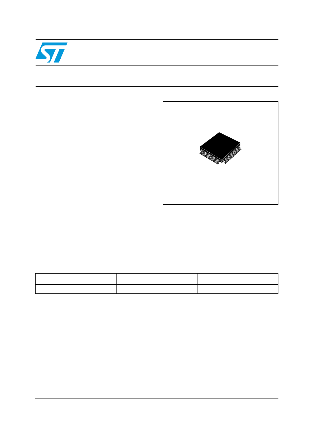
Table 1. Device summary
TDA7505
LQFP100
(14x14x1.4mm)
■ 5V-tolerant 3V I/O interface
■ Multifunction general purpose I/O ports
Description
The TDA7505 is an MPX-sampling DSP for car
radio applications.
Order code Package Packing
TDA7505 LQFP100 Tray
October 2007 Rev 1 1/38
www.st.com
1
Page 2

Contents TDA7505
Contents
1 Overview . . . . . . . . . . . . . . . . . . . . . . . . . . . . . . . . . . . . . . . . . . . . . . . . . . 6
2 Block diagram . . . . . . . . . . . . . . . . . . . . . . . . . . . . . . . . . . . . . . . . . . . . . . 7
3 Pin description . . . . . . . . . . . . . . . . . . . . . . . . . . . . . . . . . . . . . . . . . . . . . 8
4 Electrical specifications . . . . . . . . . . . . . . . . . . . . . . . . . . . . . . . . . . . . . 15
4.1 Absolute maximum ratings . . . . . . . . . . . . . . . . . . . . . . . . . . . . . . . . . . . . 15
4.2 Thermal data . . . . . . . . . . . . . . . . . . . . . . . . . . . . . . . . . . . . . . . . . . . . . . 15
4.3 Electrical characteristics . . . . . . . . . . . . . . . . . . . . . . . . . . . . . . . . . . . . . . 16
4.3.1 Recommended DC operating conditions . . . . . . . . . . . . . . . . . . . . . . . . 16
4.3.2 Power consumption . . . . . . . . . . . . . . . . . . . . . . . . . . . . . . . . . . . . . . . . 16
4.3.3 Oscillator characteristics . . . . . . . . . . . . . . . . . . . . . . . . . . . . . . . . . . . . 16
4.3.4 General interface electrical characteristics . . . . . . . . . . . . . . . . . . . . . . 17
4.3.5 High voltage CMOS interface DC electrical characteristics . . . . . . . . . . 17
4.3.6 DSP core . . . . . . . . . . . . . . . . . . . . . . . . . . . . . . . . . . . . . . . . . . . . . . . . 17
4.4 SAI interface timing - receiver . . . . . . . . . . . . . . . . . . . . . . . . . . . . . . . . . 18
4.5 SAI interface timing - transmitter . . . . . . . . . . . . . . . . . . . . . . . . . . . . . . . 18
4.6 SAI protocol . . . . . . . . . . . . . . . . . . . . . . . . . . . . . . . . . . . . . . . . . . . . . . . 19
4.7 SPDIF receiver . . . . . . . . . . . . . . . . . . . . . . . . . . . . . . . . . . . . . . . . . . . . . 19
4.8 SPI interfaces (Buffered SPI, Display SPI, RDS SPI) . . . . . . . . . . . . . . . 20
4.9 I
2
C Timing . . . . . . . . . . . . . . . . . . . . . . . . . . . . . . . . . . . . . . . . . . . . . . . . 21
4.10 DRAM/SRAM interface (EMI) . . . . . . . . . . . . . . . . . . . . . . . . . . . . . . . . . . 22
4.11 Debug port interface . . . . . . . . . . . . . . . . . . . . . . . . . . . . . . . . . . . . . . . . . 22
5 Functional description . . . . . . . . . . . . . . . . . . . . . . . . . . . . . . . . . . . . . . 27
5.1 24-bit DSP core . . . . . . . . . . . . . . . . . . . . . . . . . . . . . . . . . . . . . . . . . . . . 27
5.2 DSP peripherals . . . . . . . . . . . . . . . . . . . . . . . . . . . . . . . . . . . . . . . . . . . . 28
5.2.1 Data and program memories . . . . . . . . . . . . . . . . . . . . . . . . . . . . . . . . . 28
5.2.2 Serial audio interface (SAI) . . . . . . . . . . . . . . . . . . . . . . . . . . . . . . . . . . 29
5.2.3 Serial peripheral interface (SPI) . . . . . . . . . . . . . . . . . . . . . . . . . . . . . . . 29
5.2.4 Sony/Philips digital interface (S/PDIF) . . . . . . . . . . . . . . . . . . . . . . . . . . 29
5.2.5 I2C interface . . . . . . . . . . . . . . . . . . . . . . . . . . . . . . . . . . . . . . . . . . . . . . 30
2/38
Page 3

TDA7505 Contents
5.2.6 DRAM/SRAM interface (DEMI) . . . . . . . . . . . . . . . . . . . . . . . . . . . . . . . 30
5.2.7 Debug interface . . . . . . . . . . . . . . . . . . . . . . . . . . . . . . . . . . . . . . . . . . . 31
5.2.8 General purpose input/output . . . . . . . . . . . . . . . . . . . . . . . . . . . . . . . . 31
5.2.9 Asynchronous sample rate converter . . . . . . . . . . . . . . . . . . . . . . . . . . 31
5.2.10 SINCOS co-processor . . . . . . . . . . . . . . . . . . . . . . . . . . . . . . . . . . . . . . 31
5.2.11 PLL clock oscillator . . . . . . . . . . . . . . . . . . . . . . . . . . . . . . . . . . . . . . . . 31
5.2.12 CODEC . . . . . . . . . . . . . . . . . . . . . . . . . . . . . . . . . . . . . . . . . . . . . . . . . 32
5.2.13 Radio data system (RDS) . . . . . . . . . . . . . . . . . . . . . . . . . . . . . . . . . . . 32
5.2.14 Clock scheme . . . . . . . . . . . . . . . . . . . . . . . . . . . . . . . . . . . . . . . . . . . . 33
6 Software features . . . . . . . . . . . . . . . . . . . . . . . . . . . . . . . . . . . . . . . . . . 34
6.1 AM/FM base band signal processing . . . . . . . . . . . . . . . . . . . . . . . . . . . . 34
6.2 Generic audio signal processing . . . . . . . . . . . . . . . . . . . . . . . . . . . . . . . 34
6.3 TAPE signal processing . . . . . . . . . . . . . . . . . . . . . . . . . . . . . . . . . . . . . . 34
6.4 CD signal processing . . . . . . . . . . . . . . . . . . . . . . . . . . . . . . . . . . . . . . . . 34
6.5 Audiophile . . . . . . . . . . . . . . . . . . . . . . . . . . . . . . . . . . . . . . . . . . . . . . . . . 34
6.6 Audio decompression . . . . . . . . . . . . . . . . . . . . . . . . . . . . . . . . . . . . . . . . 34
6.7 Other . . . . . . . . . . . . . . . . . . . . . . . . . . . . . . . . . . . . . . . . . . . . . . . . . . . . 35
6.8 Functional modes . . . . . . . . . . . . . . . . . . . . . . . . . . . . . . . . . . . . . . . . . . . 35
7 Package information . . . . . . . . . . . . . . . . . . . . . . . . . . . . . . . . . . . . . . . . 36
8 Revision history . . . . . . . . . . . . . . . . . . . . . . . . . . . . . . . . . . . . . . . . . . . 37
3/38
Page 4

List of tables TDA7505
List of tables
Table 1. Device summary . . . . . . . . . . . . . . . . . . . . . . . . . . . . . . . . . . . . . . . . . . . . . . . . . . . . . . . . . . 1
Table 2. Pin description . . . . . . . . . . . . . . . . . . . . . . . . . . . . . . . . . . . . . . . . . . . . . . . . . . . . . . . . . . . 8
Table 3. Absolute maximum ratings . . . . . . . . . . . . . . . . . . . . . . . . . . . . . . . . . . . . . . . . . . . . . . . . . 15
Table 4. Thermal data. . . . . . . . . . . . . . . . . . . . . . . . . . . . . . . . . . . . . . . . . . . . . . . . . . . . . . . . . . . . 15
Table 5. Recommended DC operating conditions . . . . . . . . . . . . . . . . . . . . . . . . . . . . . . . . . . . . . . 16
Table 6. Power consumption . . . . . . . . . . . . . . . . . . . . . . . . . . . . . . . . . . . . . . . . . . . . . . . . . . . . . . 16
Table 7. Oscillator characteristics. . . . . . . . . . . . . . . . . . . . . . . . . . . . . . . . . . . . . . . . . . . . . . . . . . . 16
Table 8. General interface electrical characteristics . . . . . . . . . . . . . . . . . . . . . . . . . . . . . . . . . . . . . 17
Table 9. High voltage CMOS interface DC electrical characteristics . . . . . . . . . . . . . . . . . . . . . . . . 17
Table 10. DSP core . . . . . . . . . . . . . . . . . . . . . . . . . . . . . . . . . . . . . . . . . . . . . . . . . . . . . . . . . . . . . . 17
Table 11. SAI interface timing - receiver. . . . . . . . . . . . . . . . . . . . . . . . . . . . . . . . . . . . . . . . . . . . . . . 18
Table 12. SAI interface timing - transmitter . . . . . . . . . . . . . . . . . . . . . . . . . . . . . . . . . . . . . . . . . . . . 19
Table 13. SPDIF receiver . . . . . . . . . . . . . . . . . . . . . . . . . . . . . . . . . . . . . . . . . . . . . . . . . . . . . . . . . . 19
Table 14. SPI interfaces . . . . . . . . . . . . . . . . . . . . . . . . . . . . . . . . . . . . . . . . . . . . . . . . . . . . . . . . . . . 20
Table 15. I
Table 16. DRAM timing. . . . . . . . . . . . . . . . . . . . . . . . . . . . . . . . . . . . . . . . . . . . . . . . . . . . . . . . . . . . 22
Table 17. DRAM refresh period . . . . . . . . . . . . . . . . . . . . . . . . . . . . . . . . . . . . . . . . . . . . . . . . . . . . . 22
Table 18. SRAM Timing . . . . . . . . . . . . . . . . . . . . . . . . . . . . . . . . . . . . . . . . . . . . . . . . . . . . . . . . . . . 22
Table 19. Debug port interface . . . . . . . . . . . . . . . . . . . . . . . . . . . . . . . . . . . . . . . . . . . . . . . . . . . . . . 22
Table 20. ASRC . . . . . . . . . . . . . . . . . . . . . . . . . . . . . . . . . . . . . . . . . . . . . . . . . . . . . . . . . . . . . . . . . 24
Table 21. Fractional-N PLL. . . . . . . . . . . . . . . . . . . . . . . . . . . . . . . . . . . . . . . . . . . . . . . . . . . . . . . . . 24
Table 22. ADC electrical characteristics - measurement bandwidth 10Hz to 20kHz . . . . . . . . . . . . . 25
Table 23. ADC electrical characteristics - measurement bandwidth 10Hz to 53kHz . . . . . . . . . . . . . 25
Table 24. ADC electrical characteristics - measurement bandwidth 10Hz to 192kHz . . . . . . . . . . . . 25
Table 25. Level ADC electrical characteristics . . . . . . . . . . . . . . . . . . . . . . . . . . . . . . . . . . . . . . . . . . 25
Table 26. DAC Performance. . . . . . . . . . . . . . . . . . . . . . . . . . . . . . . . . . . . . . . . . . . . . . . . . . . . . . . . 26
Table 27. FM stereo decoder (SW) . . . . . . . . . . . . . . . . . . . . . . . . . . . . . . . . . . . . . . . . . . . . . . . . . . 26
Table 28. Examples of convenient clock schemes . . . . . . . . . . . . . . . . . . . . . . . . . . . . . . . . . . . . . . . 33
Table 29. Example of possible modes . . . . . . . . . . . . . . . . . . . . . . . . . . . . . . . . . . . . . . . . . . . . . . . . 35
Table 30. Document revision history . . . . . . . . . . . . . . . . . . . . . . . . . . . . . . . . . . . . . . . . . . . . . . . . . 37
2
C Timing. . . . . . . . . . . . . . . . . . . . . . . . . . . . . . . . . . . . . . . . . . . . . . . . . . . . . . . . . . . . . . 21
4/38
Page 5

TDA7505 List of figures
List of figures
Figure 1. Block diagram . . . . . . . . . . . . . . . . . . . . . . . . . . . . . . . . . . . . . . . . . . . . . . . . . . . . . . . . . . . . 7
Figure 2. LQFP100 pins connection (top view) . . . . . . . . . . . . . . . . . . . . . . . . . . . . . . . . . . . . . . . . . 14
Figure 3. SAI interface timing - receiver. . . . . . . . . . . . . . . . . . . . . . . . . . . . . . . . . . . . . . . . . . . . . . . 18
Figure 4. SAI interface timing - transmitter . . . . . . . . . . . . . . . . . . . . . . . . . . . . . . . . . . . . . . . . . . . . 18
Figure 5. SAI protocol . . . . . . . . . . . . . . . . . . . . . . . . . . . . . . . . . . . . . . . . . . . . . . . . . . . . . . . . . . . . 19
Figure 6. SPI interfaces . . . . . . . . . . . . . . . . . . . . . . . . . . . . . . . . . . . . . . . . . . . . . . . . . . . . . . . . . . . 20
Figure 7. SPI clocking scheme . . . . . . . . . . . . . . . . . . . . . . . . . . . . . . . . . . . . . . . . . . . . . . . . . . . . . 21
Figure 8. I
Figure 9. Debug port serial clock timing . . . . . . . . . . . . . . . . . . . . . . . . . . . . . . . . . . . . . . . . . . . . . . . 23
Figure 10. Debug port acknowledge timing . . . . . . . . . . . . . . . . . . . . . . . . . . . . . . . . . . . . . . . . . . . . . 23
Figure 11. Debug port data I/O to status timing . . . . . . . . . . . . . . . . . . . . . . . . . . . . . . . . . . . . . . . . . . 23
Figure 12. Debug port read timing . . . . . . . . . . . . . . . . . . . . . . . . . . . . . . . . . . . . . . . . . . . . . . . . . . . . 24
Figure 13. Debug port DBCK next command after read register timing. . . . . . . . . . . . . . . . . . . . . . . . 24
Figure 14. LQFP100 (14x14x1.4mm) mechanical data and package dimensions. . . . . . . . . . . . . . . . 36
2
C Timing. . . . . . . . . . . . . . . . . . . . . . . . . . . . . . . . . . . . . . . . . . . . . . . . . . . . . . . . . . . . . . 21
5/38
Page 6

Overview TDA7505
1 Overview
The TDA7505 integrates two 75 MIPS DSP cores. One core is used for stereo decoding,
noise blanking, weak signal processing, Dolby B, music search and MP3 decoding. The
second core is used for audio and sound processing and Echo & Noise cancellation. All
functions are realized in SW and thus are flexible on customer request.
The device may be controlled by a main micro through either SPI or I
the same pins, but with separate device address (I
2
C) respectively separate chip select line
(SPI) the main micro may communicate with the DSP or with the RDS block.
An additional SPI is available allowing a separate communication (e.g. to a display micro).
The DSP cores are integrated with their associated data and program memories.
DSP0 is declared as master. Its associated peripherals and interfaces are: I
(Master SPI), SPI2 (Display SPI), Serial Audio Interface (SAI), PLL Oscillator, External
Memory Interface (EMI), General Purpose I/O ports (DSP0 GPIO[0..11]), RDS filter and D/A
converters.
DSP1 is declared as Co-DSP. Its associated peripherals and interfaces are: A/D converters,
SPDIF, Sample Rate Converter (SRC) and General Purpose I/O ports (DSP1 GPIO[0..11]).
Both DSP´s are identical (ST Orpheus core, 75 MHz clock). Only the peripherals and
memory configurations are different. The internal communication takes place through a bidirectional 24/10-word exchange interface (XCHG) with complex flag and interrupts
capability.
2
C interface. Through
2
C, SPI1
The Radio Data System (RDS, respectively RBDS) function is realized via dedicated
hardware. It may run fully autonomous without SW intervention. Thus an efficient
background mode as well as a low current standby mode is possible. The RDS input is
connected to the A/D converter to receive the FM multiplex signal (MPX) automatically. Its
output may be configured to I
2
C or SPI format. The pins are shared with the I2C and SPI1 of
DSP0.
The device is equipped with a debug and test interface. It allows the SW development with a
100% compatible emulation system.
All functions, except RDS, are implemented in SW. Thus, the device may be adapted to
customers´ requirements. This implies the variable implementation of SW modules
developed by the customer, ST and third parties. This flexibility also allows the usage for
applications others than car radios, e.g.: Boosters.
6/38
Page 7
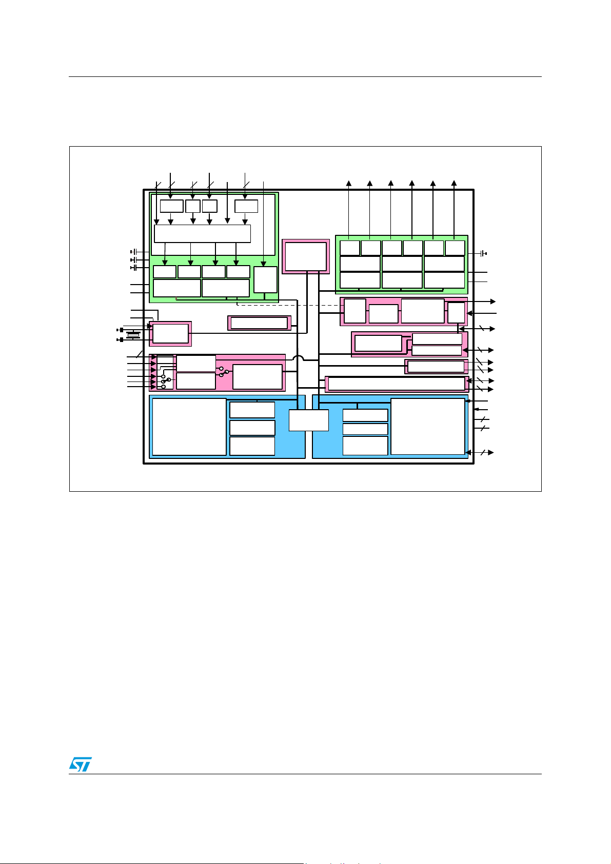
TDA7505 Block diagram
μ
μ
Σ
/
2 Block diagram
Figure 1. Block diagram
analog audio in
ADC - ref
ADCVDD
ADCGND
AVDD
AGND
CLK in
8.55 MHz
6 Ch. Audio B us
receive bit&word clk
digital audio in
SPDIF audio in
CC
2
Qdiff
ΣΔ
Decimation
Audio
Crystal
Oscillator
2
DSP1 Orpheus Cor e
Including 12 GPIO´s
AM processing,
FM processing,
CD compression,
Dolby B
MP3
Debug Interface
CD
Navi
Tel.
2
4
.
Input Source Selector
Diff .
Diff .
Δ ΣΔ ΣΔ
Decimation
FM/Audio
SAI 6ch.
Receiver
SPDIF 2ch.
Interface
,
.
2
Mpx
AM/FM
RDS
Qdiff
SINCOS
2ch sample
rate converter
X Ram 4096
X Rom 4096
Y Ram 40969
P Ram
P Rom 16384
M
AM
3
.
4096
px
FMLevel
AM/FM
level
ADC
PLL Clock
Generator
Xchg
Interface
analog audio out
SC
FilterSCFilter
Noise
Shaper
Oversampl.
Filter
RDS
Filter
External Memory Interface
X Ram
Y Ram
P Ram
P Rom 16384
SC
FilterSCFilter
Oversampl.
Filter
Demod
10 word SPI 1
receive stack
4096
4096
4096
Noise
Shaper
.
SC
SC
Filter
Filter
Noise
Shaper
Oversampl .
Filter
Grp&blk
sync., error
correction
IIC / SPI 1
SPI 2
SAI Transmit ter
SRAM 4Mx
DRAM 64Mx4
DSP0 Orpheus Core
Including 12 GPIO´s
Audio processing,
Sound processing,
TAM,
Echo & noise
SPI
IIC
8
cancell
Debug Interface
-
DAC
ref
DACVDD
DACGND
4
4
3
2
8+3
17
4
4
Debug
5
RDS Int.
RDSCS
P
control
Display
6 Channel
Audio Bus
INT
NRESET
VDD
GND
/
Test
P
/
.
7/38
Page 8
Pin description TDA7505
3 Pin description
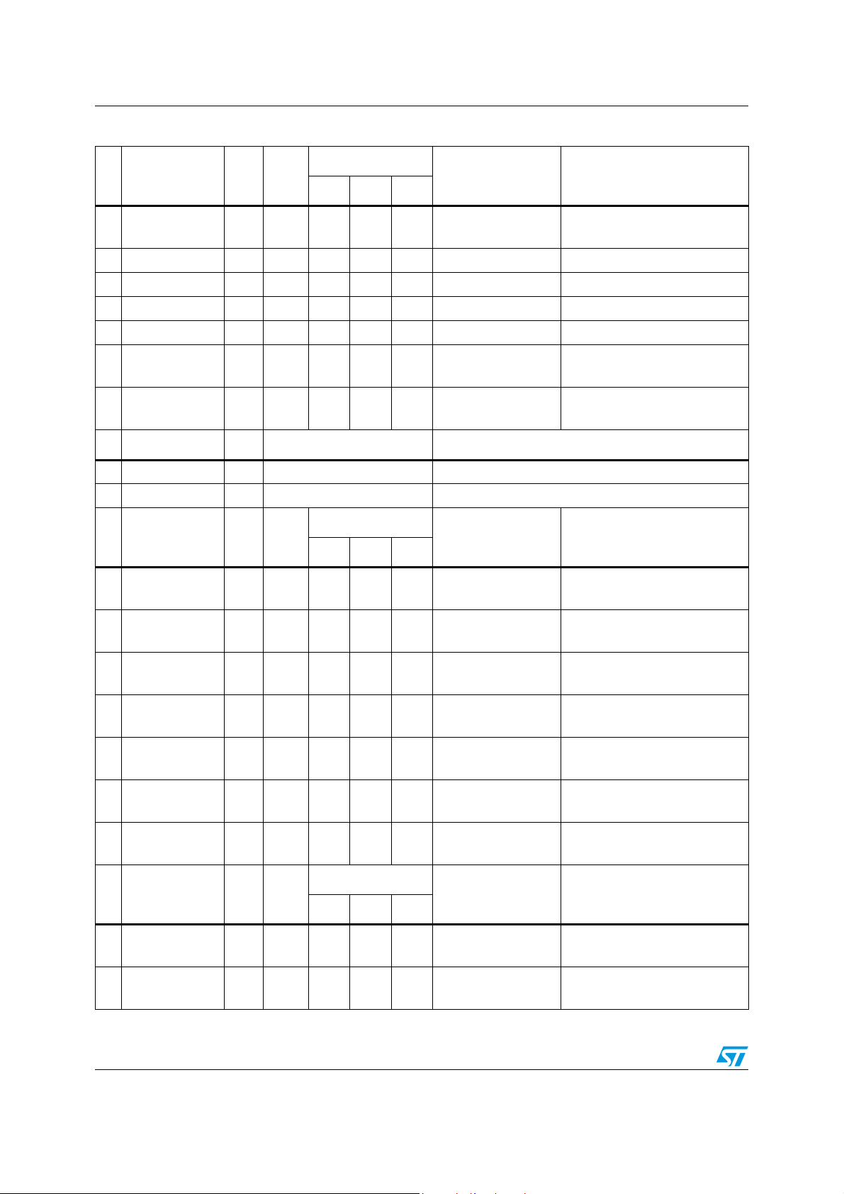
Table 2. Pin description
N° Name Type Function
1 DAC4 A Signal output D/A converter (single ended)
2 DAC5 A Signal output D/A converter (single ended)
N° Name Type Voltage Function
3 VDD1V8_1 S 1.8V Digital Supply dedicated to internal logic
4 GND1V8_1 S 0V Digital Ground dedicated to internal logic
N° Name Type
5 NRESET I E0 E1 E1 E1 Input 5VT
SRCCD
6
MISOD output
MISOD input
SRCMD
MOSID input
7
MOSID output
DSP0 GPIO0
DSP0 GPIO0
Reset
state
I/OZ ZZZ
I/O
Z ZZZ
After boot with
2
SPI I
C * EMI
I/O Function
Input 5VT
Output 2mA PP/OD
Input 5VT
Input 5VT
Input 5VT
Output 2mA PP
Input 5VT
Output 2mA PP
System Reset. A low level
applied to NRESET input
initializes the IC.
SPDIF input source 1 (e.g.: CD)
Display SPI SO (slave mode)
Display SPI MI (master mode)
SPDIF input source 2 (e.g.: MD)
Display SPI SI (slave mode)
Display SPI MO (master mode)
GPIO input
GPIO output
SSD input
INT
8
DSP0 GPIO1
DSP0 GPIO1
CLKIN
9
SCKD input
SCKD output
N° Name Type Voltage Function
10 AVDD S 3.3V Supply dedicated to the PLL
11 XTI A AC Crystal oscillator input
12 XTO A AC Crystal oscillator output
13 AGND S 0V Ground dedicated to the PLL
I/O
I/OZ ZZZ
Z ZZZ
Input 5VT
Input 5VT
Input 5VT
Output 2mA PP
Input 5VT
Input 5VT
Output 2mA PP
Display SPI SS slave select
DSP0 external interrupt (IRQA)
GPIO input
GPIO output
External clock input for PLL
Display SPI clock (slave mode)
Display SPI clock (master mode)
8/38
Page 9
TDA7505 Pin description
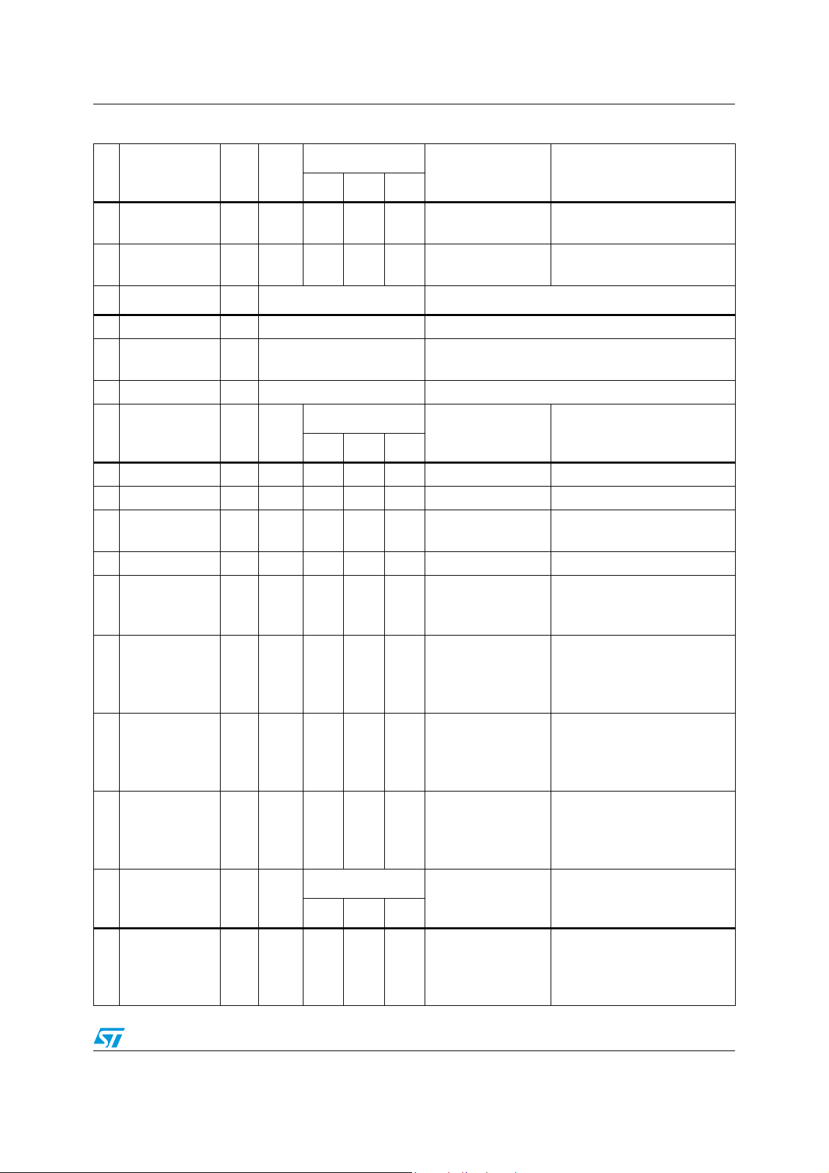
Table 2. Pin description (continued)
After boot with
2
SPI I
C * EMI
I/O Function
Input 5VT
Output 2mA OD
Input 5VT
Output 2mA PP
Input 5VT
Output 2mA OD
Output 2mA PP
Input 5VT
Output 2mA PP
RDS SPI CS chip select in
RDS bit data
GPIO input
GPIO output
DSP0 external interrupt (IRQA)
RDS bit clock
RDS Interrupt Output
GPIO input
GPIO output
N° Name Type
RDSCS
-
14
DSP0 GPIO2
I/O
DSP0 GPIO2
INT
-
15
RDSINT
I/O
DSP0 GPIO3
DSP0 GPIO3
Reset
State
Z ZZZ
Z ZZZ
N° Name Type Voltage Function
16 VDD3V3_1 S 3.3V Digital supply dedicated to I/O structures
17 GND3V3_1 S 0V Digital ground dedicated to I/O structures
SCKM input
SCKM output
18
SCL bi-direct
DSP0 GPIO4
DSP0 GPIO4
I/O
Z
0/1 Z
Input 5VT
Output 2mA PP
In 5VT/Out 2mA OD
Z
Input 5VT
Output 2mA PP
Master/RDS SPI clock (slave m.)
Master SPI clock (master mode)
I2C clock
GPIO input
GPIO output
N° Name Type
MISOM output
MISOM input
19
ADDR select
I/O
DSP0 GPIO5
DSP0 GPIO5
MOSIM input
MOSIM output
20
SDA bi-direct
I/O
DSP0 GPIO6
DSP0 GPIO6
SSM input
21
DSP0 GPIO7
I/O Z
DSP0 GPIO7
DSRA<0>
22
23
24
DSRA<0>
DSRA<1>
DSRA<1>
DSRA<2>
DSRA<2>
I/O 0 1 1 Z
I/O 0 1 1 Z
I/O 0 1 1 Z
Reset
state
Z
Z
After boot with
2
SPI I
C * EMI
0/1 Z
0/1 Z
Z
ZZ
Output 2mA PP/OD
Input 5VT
Input 5VT
Z
Input 5VT
Output 2mA PP
Input 5VT
Output 2mA PP
In 5VT/Out 2mA OD
Z
Input 5VT
Output 2mA PP
Input 5VT
Input 5VT
Output 2mA PP
In/Out 2mA PP
In/Out 2mA PP
In/Out 2mA PP
In/Out 2mA PP
In/Out 2mA PP
In/Out 2mA PP
I/O Function
Master/RDS SPI SO (slave m.)
Master SPI MI (master mode)
2
C Address select line
I
GPIO input
GPIO output
Master/RDS SPI SI (slave m.)
Master SPI MO (master mode)
2
C data
I
GPIO input
GPIO output
Master SPI SS slave select
GPIO input
GPIO output
EMI SRAM Data 0
EMI DRAM Data 0
EMI SRAM Data 1
EMI DRAM Data 1
EMI SRAM Data 2
EMI DRAM Data 2
9/38
Page 10
Pin description TDA7505
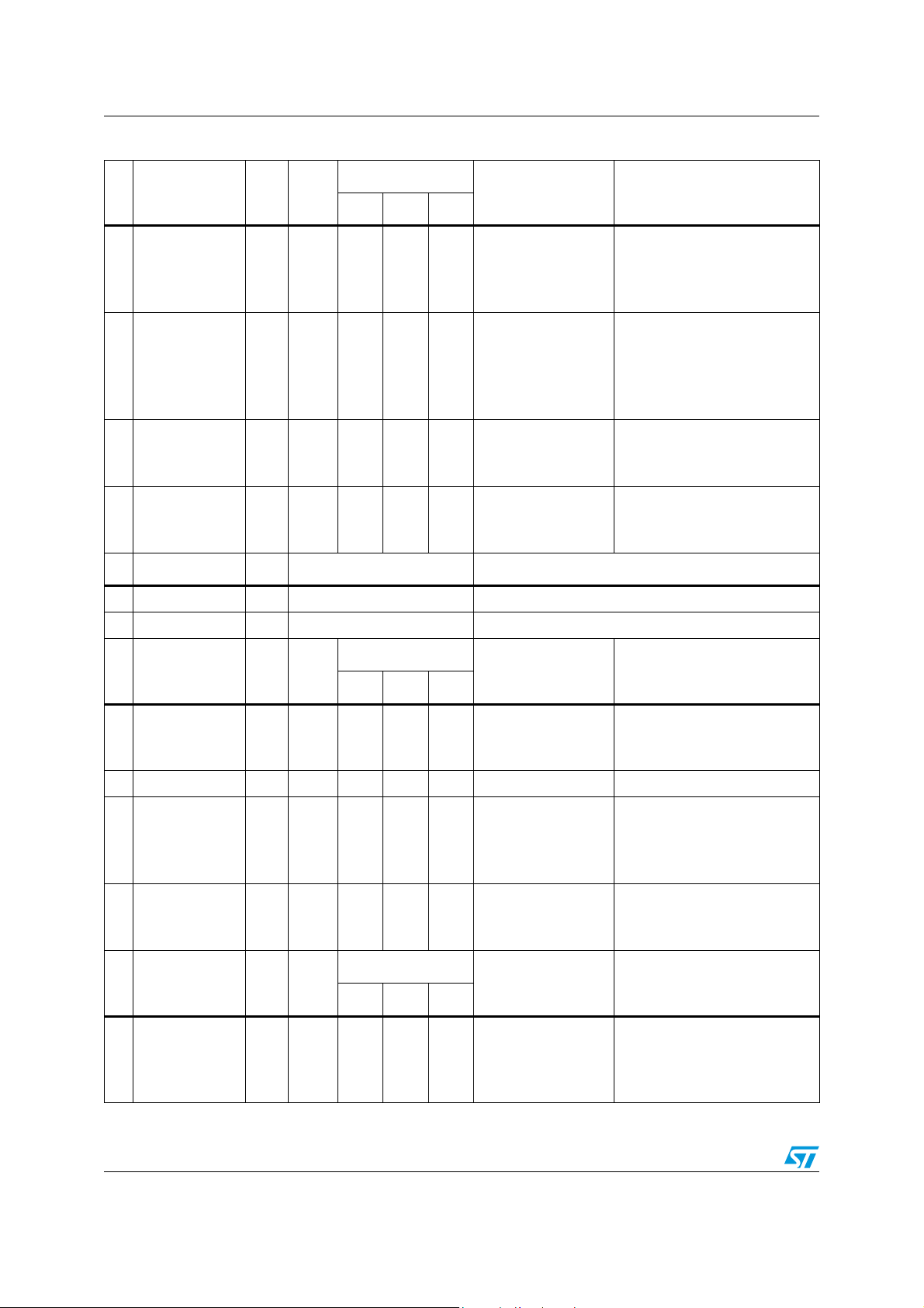
Table 2. Pin description (continued)
After boot with
2
SPI I
C * EMI
I/O Function
In/Out 2mA PP
In/Out 2mA PP
EMI SRAM Data 3
EMI DRAM Data 3
N° Name Type
DSRA<3>
25
DSRA<3>
I/O 0 1 1 Z
Reset
state
26 DSRA<4> I/O 0 1 1 Z In/Out 2mA PP EMI SRAM Data 4
27 DSRA<5> I/O 0 1 1 Z In/Out 2mA PP EMI SRAM Data 5
28 DSRA<6> I/O 0 1 1 Z In/Out 2mA PP EMI SRAM Data 6
29 DSRA<7> I/O 0 1 1 Z In/Out 2mA PP EMI SRAM Data 7
30
31
SRA<0>
SRA<0>
SRA<1>
SRA<1>
O0 110/1
O0 110/1
Output 2mA PP
Output 2mA PP
Output 2mA PP
Output 2mA PP
EMI SRAM Address 0
EMI DRAM Address 0
EMI SRAM Address 1
EMI DRAM Address 1
N° Name Type Voltage Function
32 VDD3V3_2 S 3.3V Digital Supply dedicated to I/O structures
33 GND3V3_2 S 0V Digital Ground dedicated to I/O structures
After boot with
2
SPI I
C * EMI
I/O Function
N° Name Type
Reset
state
SRA<2>
34
35
36
37
38
39
40
SRA<2>
SRA<3>
SRA<3>
SRA<4>
SRA<4>
SRA<5>
SRA<5>
SRA<6>
SRA<6>
SRA<7>
SRA<7>
SRA<8>
SRA<8>
O0 110/1
O0 110/1
O0 110/1
O0 110/1
O0 110/1
O0 110/1
O0 110/1
N° Name Type
SRA<9>
41
42
SRA<9>
SRA<10>
SRA<10>
O0 110/1
O0 110/1
Reset
state
After boot with
2
SPI I
C * EMI
Output 2mA PP
Output 2mA PP
Output 2mA PP
Output 2mA PP
Output 2mA PP
Output 2mA PP
Output 2mA PP
Output 2mA PP
Output 2mA PP
Output 2mA PP
Output 2mA PP
Output 2mA PP
Output 2mA PP
Output 2mA PP
I/O Function
Output 2mA PP
Output 2mA PP
Output 2mA PP
Output 2mA PP
EMI SRAM Address 2
EMI DRAM Address 2
EMI SRAM Address 3
EMI DRAM Address 3
EMI SRAM Address 4
EMI DRAM Address 4
EMI SRAM Address 5
EMI DRAM Address 5
EMI SRAM Address 6
EMI DRAM Address 6
EMI SRAM Address 7
EMI DRAM Address 7
EMI SRAM Address 8
EMI DRAM Address 8
EMI SRAM Address 9
EMI DRAM Address 9
EMI SRAM Address 10
EMI DRAM Address 10
10/38
Page 11
TDA7505 Pin description
Table 2. Pin description (continued)
After boot with
2
SPI I
C * EMI
I/O Function
Output 2mA PP
Output 2mA PP
Output 2mA PP
Output 2mA PP
EMI SRAM Address 11
EMI DRAM Address 11
EMI SRAM Address 12
EMI DRAM Address 12
N° Name Type
SRA<11>
43
44
SRA<11>
SRA<12>
SRA<12>
O0 110/1
O0 110/1
Reset
state
N° Name Type Voltage Function
45 VDD1V8_2 S 1.8V Digital Supply dedicated to internal logic
GND1V8_2 &
46
GND3V3_3
S0V
Digital Ground dedicated to internal logic and I/O
structures
47 VDD3V3_3 S 3.3V Digital Supply dedicated to I/O structures
After boot with
2
SPI I
C * EMI
I/O Function
N° Name Type
Reset
state
48 DRD O 1 1 1 1 Output 2mA PP EMI data read strobe
49 DWR O 1 1 1 1 Output 2mA PP EMI data write strobe
50
CAS
SRA<13>
O
0110/1
Output 2mA PP
Output 2mA PP
EMI DRAM CAS
EMI SRAM Address 13
51 SRA<14> O 0 1 1 0/1 Output 2mA PP EMI SRAM Address 14
SRA<15>
52
DSP0 GPIO8
DSP0 GPIO8
INOUTA
SRA<16>
53
DSP1 GPIO0
DSP1 GPIO0
INOUTB
SRA<17>
54
DSP1 GPIO1
DSP1 GPIO1
I/O Z Z Z 0/1
I/O
I/O
ZZZ0/1
ZZZ0/1
Output 2mA PP
Input 5VT
Output 2mA PP
In 5VT/Out 2mA PP
Output 2mA PP
Input 5VT
Output 2mA PP
In 5VT/Out 2mA PP
Output 2mA PP
Input 5VT
Output 2mA PP
EMI SRAM Address 15
GPIO input
GPIO output
Multi function I/O
EMI SRAM Address 16
GPIO input
GPIO output
Multi function I/O
EMI SRAM Address 17
GPIO input
GPIO output
INOUTC
SRA<18>
55
DSP1 GPIO2
I/O
DSP1 GPIO2
N° Name Type
INOUTD
SRA<19>
56
DSP1 GPIO3
I/O
DSP1 GPIO3
ZZZ0/1
Reset
state
After boot with
2
SPI I
C * EMI
0/1
ZZZ
In 5VT/Out 2mA PP
Output 2mA PP
Input 5VT
Output 2mA PP
Multi function I/O
EMI SRAM Address 18
GPIO input
GPIO output
I/O Function
In 5VT/Out 2mA PP
Output 2mA PP
Input 5VT
Output 2mA PP
Multi function I/O
EMI SRAM Address 19
GPIO input
GPIO output
11/38
Page 12
Pin description TDA7505
Table 2. Pin description (continued)
After boot with
2
SPI I
C * EMI
Z
In 5VT/Out 2mA PP
0/1
Output 2mA PP
Input 5VT
Output 2mA PP
In 5VT/Out 2mA PP
0/1
Output 2mA PP
Output 2mA PP
Input 5VT
Output 2mA PP
In 5VT/Out 2mA PP
Input 5VT
Output 2mA PP
In 5VT/Out 2mA PP
Input 5VT
Output 2mA PP
I/O Function
Multi function I/O
EMI SRAM Address 20
GPIO input
GPIO output
Multi function I/O
EMI SRAM Address 21
EMI DRAM RAS
GPIO input
GPIO output
Multi function I/O
GPIO input
GPIO output
Multi function I/O
GPIO input
GPIO output
N° Name Type
INOUTE
SRA<20>
57
DSP1 GPIO4
I/O
DSP1 GPIO4
INOUTF
SRA<21>
58
RAS
I/O
DSP1 GPIO5
DSP1 GPIO5
INOUTG
59
DSP1 GPIO6
I/OZ ZZZ
DSP1 GPIO6
INOUTH
60
DSP1 GPIO7
I/OZ ZZZ
DSP1 GPIO7
Reset
state
ZZ
ZZZ
N° Name Type Voltage Function
61 VDD3V3_4 S 3.3V Digital Supply dedicated to I/O structures
62 GND3V3_4 S 0V Digital Ground dedicated to I/O structures
After boot with
2
SPI I
C * EMI
I/O Function
In 5VT/Out 2mA PP
Input 5VT
Output 2mA PP
Multi function I/O
GPIO input
GPIO output
N° Name Type
INOUTI
63
DSP1 GPIO8
I/OZ ZZZ
DSP1 GPIO8
Reset
state
64 INOUTJ I/O Z Z Z Z In 5VT/Out 2mA PP Multi function I/O
DBCK
OS1
65
DSP0/1 GPIO9
I/O
DSP0/1 GPIO9
DBOUT
66
DSP0/1 GPIO10
I/O
DSP0/1 GPIO10
N° Name Type
DBIN
OS0
67
DSP0/1 GPIO11
I/O
DSP0/1 GPIO11
Z
Z
Reset
state
Z
000
111
After boot with
2
SPI I
C * EMI
000
Input 5VT
Out 2mA PP
Input 5VT
Output 2mA PP
Output 2mA PP
Input 5VT
Output 2mA PP
I/O Function
Input 5VT
Out 2mA PP
Input 5VT
Output 2mA PP
Debug clock
Chip status 1
GPIO input
GPIO output
Debug output
GPIO input
GPIO output
Debug input
Chip status 0
GPIO input
GPIO output
12/38
Page 13

TDA7505 Pin description
Table 2. Pin description (continued)
N° Name Type
Debug/Test_Sel0
68
69
Debug/Test_Sel1
70 INOUTK I/O 0 0 0 0 In 5VT/Out 2mA PP Multi function I/O
N° Name Type Voltage Function
71 VDD1V8_3 S 1.8V Digital Supply dedicated to internal logic
72 GNDSUB_D S 0V Digital substrate Ground
N° Name Type Function
73 LEVEL_AM/FM A Signal input to level ADC (single ended)
74 MPX_AM+ A Signal input tuner AM (quasi differential)
75 MPX_AM/FM- A Signal input tuner common ground (quasi differential)
76 MPX_FM+ A Signal input tuner FM (quasi differential)
77 MPX_RDS A Signal input background tuner (for RDS) single ended
78 Navi- A Signal input from navigation system (differential)
79 Navi+ A Signal input from navigation system (differential)
80 Phone- A Signal input from Telephone (differential)
81 Phone+ A Signal input from Telephone (differential)
Reset
state
I E1 E1 E1 E1 Input Mode select (Debug0/1, Test)
I E1 E1 E1 E1 Input Mode select (Debug0/1, Test)
After boot with
2
SPI I
C * EMI
I/O Function
N° Name Type Voltage Function
82 ADCGND S 0V Analog Ground dedicated to the A/D converter
83 ADCVDD S 3.3V Analog Supply dedicated to the A/D converter
N° Name Type Function
84 ADCREF3 A ADC reference voltage decoupling
85 CD_R+ A Signal right input from CD-changer (differential)
86 CD_R- A Signal right input from CD-changer (differential)
87 ADCREF2 A ADC reference voltage decoupling
88 CD_L- A Signal left input from CD-changer (differential)
89 CD_L+ A Signal left input from CD-changer (differential)
90 ADCREF1 A ADC reference voltage decoupling
91 CC_R A Signal right input from cassette (single ended)
92 CC_L A Signal left input from cassette (single ended)
N° Name Type Voltage Function
93 GNDSUB_A S 0V Analog substrate Ground
94 DACVDD S 3.3V Analog Supply dedicated to the D/A converter.
13/38
Page 14

Pin description TDA7505
Table 2. Pin description (continued)
N° Name Type Function
95 DACREF A DAC reference voltage decoupling
N° Name Type Voltage Function
96 DACGND S 0V Analog Ground dedicated to the D/A converter.
N° Name Type Function
97 DAC0 A Signal output D/A converter (single ended)
98 DAC1 A Signal output D/A converter (single ended)
99 DAC2 A Signal output D/A converter (single ended)
100
DAC3 A Signal output D/A converter (single ended)
Type: S: Supply pin 0: logic low output PP: push-pull
I: Digital Input pin 1: logic high output OD: open drain
O: Digital Output pin E0: logic low input 5VT: 5 volt tolerant
A: Analog pin E1: logic high input Schmitt-trigger on all inputs
Z: high impedance (Input mode of bi-directional pin)
2
C Master boot mode, using multiplexed debug interface (pin15: INT/RDSINT = 1, pin21: SSM = 0, pin52:
*) I
SRA15 = 0)
Figure 2. LQFP100 pins connection (top view)
DACREF
DACVDD
DAC0
DACGND
DSP0 GPIO0
DSP0 GPIO1
DSP0 GPIO2
DSP0 GPIO3
DSP0 GPIO4
DSP0 GPIO5
DSP0 GPIO6
DSP0 GPIO7
DAC4
DAC5
VDD1V8_1
GND1V8_1
NRESET
SRCCD/MISOD
SRCMD/MOSID
INT/SSD
CLKIN/SCKD
AVDD
XTI
XTO
AGND
RDSCS
INT/RDSINT
VDD3V3_1
GND3V3_1
SCL/SCKM
ADDR/MISOM
SDA/MOSIM
SSM
DSRA<0>
DSRA<1>
DSRA<2>
DSRA<3>
1
2
3
4
5
6
7
8
9
10
11
12
13
14
15
16
17
18
19
20
21
22
23
24
25
DAC2
DAC3
99
100
SPDIF
DSPI
PLL
RDS
Bootsel0
BSPI/I2C
Bootsel1
27
26
DSRA<4>
DSRA<5>
DAC1
97
98
28
29
DSRA<6>
DSRA<7>
GNDSUB_A
96
94
93
95
TDA7505
33
303132
SRA<0>
SRA<1>
VDD3V3_2
GND3V3_2
CC_L
ADCREF1
CC_R
CD_L+
92
898887
90
91
CODEC
EMI
373839
34
36
35
SRA<3>
SRA<2>
SRA<4>
SRA<5>
ADCREF2
CD_L-
SRA<6>
SRA<7>
CD_R-
CD_R+
ADCREF3
ADCVDD
84
86
83
85
4041424344
SRA<8>
SRA<9>
SRA<10>
SRA<11>
Phone-
Phone+
ADCGND
8180797877
82
Debug/Te st
SAI/SPDIF
Bootsel2
4546474849
SRA<12>
VDD1V8_2
Navi-
MPX_RDS
MPX_FM+
Navi+
76
MPX_AM/FM-
75
MPX_AM+
74
LEVEL_A M/FM
73
GNDSUB_D
72
VDD1V8_3
71
INOUTK
70
Debug/Test_Sel1
69
68
Debug/Test_Sel0
67
DBIN_OS0
66
DBOUT
DBCK_OS1
65
64
INOUTJ
63
INOUTI
62
GND3V3_4
61
VDD3V3_4
INOUTH
60
59
INOUTG
58
INOUTF/SRA<21>/RAS
57
INOUTE/SRA<20>
INOUTD/SRA<19>
56
INOUTC/SRA<18>
55
54
INOUTB/SRA<17>
53
INOUTA/SRA<16>
52
SRA<15>
51
SRA<14>
50
DRD
DWR
VDD3V3_3
CAS/SRA<13>
DSP0/1 GPIO11
DSP0/1 GPIO10
DSP0/1 GPIO9
DSP1 GPIO8
DSP1 GP IO7
DSP1 GPIO6
DSP1 GPIO5
DSP1 GPIO4
DSP1 GPIO3
DSP1 GP IO2
DSP1 GP IO1
DSP1 GPIO0
DSP0 GPIO8
14/38
GND1V8_2/GND3V3_3
Page 15

TDA7505 Electrical specifications
4 Electrical specifications
4.1 Absolute maximum ratings
Table 3. Absolute maximum ratings
Symbol Parameter Value Unit
VDD1V8
VDD3V3
AVDD
DACVDD
ADCVDD
Power supplies digital
I/O
Analog
DAC
ADC
Analog input or output voltage -0.5 to (AVDD+0.5)
Digital input or output voltage, 5V tolerant
T
T
1. The maximum difference in the voltage of AVDD, DACVDD, ADCVDD, analog inputs and analog outputs
must not exceed 0.5V. Warning: Operation at or beyond these limits may result in permanent damage to
the device. Normal operation is not guaranteed at these extremes.
2. During Normal Mode operation VDD3 is always available as specified.
3. During Fail-save Mode operation VDD3 may be not available.
Operating temperature range -40 to 85 °C
op
Storage temperature -55 to 150 °C
stg
4.2 Thermal data
Table 4. Thermal data
Symbol Parameter Value Unit
R
th j-amb
R
th j-case
1. In still air
2. Measured on top side of the package
Thermal resistance junction to ambient
T
Operating junction temperature 125 °C
j
Thermal junction to case
(2)
(1)
Normal
Fail-safe
(2)
(3)
-0.5 to +1.95
-0.5 to +3.6
-0.5 to +3.6
-0.5 to +3.6
-0.5 to +3.6
(1)
(1)
(1)
-0.5 to 6.3
-0.5 to 3.8
55 °C/W
10 °C/W
(1)
V
V
V
V
V
V
V
V
15/38
Page 16

Electrical specifications TDA7505
4.3 Electrical characteristics
4.3.1 Recommended DC operating conditions
Table 5. Recommended DC operating conditions
Symbol Parameter Test condition Min. Typ. Max. Unit
VDD1V8 Digital supply voltage 1.7 1.8 1.9 V
VDD3V3 I/O supply voltage 3.15 3.3 3.49 V
AVDD Analog supply voltage 3.15 3.3 3.49 V
DACVDD D/A supply voltage 3.15 3.3 3.49 V
ADCVDD A/D supply voltage 3.15 3.3 3.49 V
4.3.2 Power consumption
Table 6. Power consumption
Symbol Parameter Test condition Min. Typ. Max. Unit
I
dd
I
dio
I
DAC
I
ADC
Note: 75MHz internal DSP clock, all CODEC channels enabled at T
Maximum current Digital power supply @ 1.8V 195 mA
Maximum current Digital IO power supply @ 3.3V 6 mA
Maximum current DAC analog power supply @ 3.3V 22 mA
Maximum current ADC analog power supply @ 3.3V 43 mA
= 25 °C
amb
4.3.3 Oscillator characteristics
Table 7. Oscillator characteristics
Symbol Parameter Test condition Min. Typ. Max. Unit
F
OSC
F
EXT
F
CLKIN
1. RDS works only with 8.55Mhz quartz or alternative with 74.1MHz applied externally on XTI pin.
2. An alternative clock input (pin CLKIN) can be used for PLL to adjust the audio sampling rate. RDS can work in parallel with
the 8.55MHz quartz.
Crystal oscillator frequency
External oscillator frequency connected through pin XTI
(1)
(1)
External oscillator frequency connected through pin CLKIN
(2)
8.55 MHz
75 MHz
80 MHz
16/38
Page 17

TDA7505 Electrical specifications
4.3.4 General interface electrical characteristics
Table 8. General interface electrical characteristics
Symbol Parameter Test condition Min. Typ. Max. Unit
Low level input current without pull-up
l
il
device
High level input current without pull-up
l
ih
device
Tri-state output leakage without pull
I
oz
up/down device
I
ozFT
I
latchup
V
1. The leakage currents are generally very small, <1nA. The value given here, 1 A, is a maximum that can occur after an
electrostatic stress on the pin.
2. Human Body Model.
5V tolerant tri-state output leakage
without pull up/down device
I/O latch-up current Vi < 0V, Vi > V
Electrostatic protection Leakage, 1μA
esd
(1)
= 0V
V
i
DD3V3
(1)
DD3V3
DD3V3
DD3V3
(2)
(1)
(1)
200 mA
2000 V
= V
V
i
V
= 0V or V
o
= 0V or V
V
o
= 5.5V 1 7 μA
V
o
1 μA
1 μA
1 μA
1 μA
4.3.5 High voltage CMOS interface DC electrical characteristics
Table 9. High voltage CMOS interface DC electrical characteristics
Symbol Parameter Test condition Min. Typ. Max. Unit
Low Level Input Voltage 3.0V<V
V
il
V
V
V
V
1. Takes into account 200mV voltage drop in both supply lines.
2. X is the source/sink current under worst-case conditions and is depicted for every I/O or output pin in the pin description.
High Level Input Voltage 3.0V<V
ih
Schmitt trigger hysteresis 3.0V<V
hyst
Low level output Voltage Iol = XmA
ol
High level output Voltage 0.89*V
oh
<3.6V 0.3*V
DD3V3
<3.6V 0.5*V
DD3V3
<3.6V 0.8 V
DD3V3
(1),(2)
DD3V3
0.1*V
DD3V3
DD3V3
DD3V3
4.3.6 DSP core
Table 10. DSP core
Symbol Parameter Test condition Min. Typ. Max. Unit
F
dsp
T
res
DSP clock frequency 75 MHz
Reset signal low state duration 1 µs
V
V
V
V
17/38
Page 18

Electrical specifications TDA7505
4.4 SAI interface timing - receiver
Figure 3. SAI interface timing - receiver
SDI0-2
LRCKR
SCKR
(RCKP=0)
t
sckrl
Table 11. SAI interface timing - receiver
Valid
Valid
t
lrckrs
t
sdis
t
t
lrckrh
sdih
t
sckr
t
sckrh
Timing Description Min Typ Max Unit
(1)
T
1. T
DSP
t
t
lrckrs
t
lrckrh
t
t
t
sckrh
t
Internal DSP clock period (typical 1/75MHz) 13.33 ns
Minimum clock cycle 6 T
sckr
LRCKR setup time T
LRCKR hold time T
SDI setup time T
sdid
SDI hold time T
sdih
Minimum SCKR high time 0.35 t
Minimum SCKR low time 0.35 t
sckrl
= DSP master clock cycle time = 1/F
DSP
dsp
DSP
DSP
DSP
DSP
DSP
sckr
sckr
ns
ns
ns
ns
ns
ns
ns
4.5 SAI interface timing - transmitter
Figure 4. SAI interface timing - transmitter
t
Valid
lrckts
SDO0-2
LRCKT
SCKT
(TCKP=0)
t
dt
t
scktl
18/38
Valid
t
lrckth
t
sckt
t
sckth
Page 19

TDA7505 Electrical specifications
Table 12. SAI interface timing - transmitter
Timing Description Min Typ Max Unit
(1)
T
1. T
DSP
t
t
lrckts
t
lrckth
t
sckth
t
Internal DSP clock period (typical 1/75MHz) 13.33 ns
Minimum clock cycle 6 T
sckt
LRCKT setup time T
LRCKT hold time T
SCKT active edge to data out valid T
t
dt
Minimum SCKT high time 0.35 t
Minimum SCKT low time 0.35 t
scktl
= DSP master clock cycle time = 1/F
DSP
dsp
DSP
DSP
DSP
DSP
sckr
sckr
ns
ns
ns
ns
ns
ns
4.6 SAI protocol
Figure 5. SAI protocol
SCKX
SCKX
LRCKX
LRCKX
LRCKX
SDY0-2
SDY0-2
Notes:1) X = R for receiver X = T for transmitter
2) Y = I for receiver Y = O for transmitter
XCKP = 0
XCKP = 1
XREL = 0
XLRS = 0
XREL = 0
XLRS = 1
XREL = 1
XLRS = 0
XDIR = 0
XDIR = 1
4.7 SPDIF receiver
Table 13. SPDIF receiver
LEFT CHANNEL
15
31 1430 1329
2 1 0
6 5 4 3 2 1 0
10
11
12
9
26
25
14
13
27
28
30
29
01
15
14
31
30
15
31
15
31 1430 1329
RIGHT CHANNEL
6 5 4 3 2 1 0
10
11
12
9
2 1 0
26
27
28
25
15
14
13
31
30
29
15
14
13
29
1 0 2
31
30
Symbol Parameter Test condition Min Typ Max Unit
f
spdif
Input sampling rate F
= 75 MHz 32 96 kHz
dsp
Input precision with direct interface to DSP 24 bit
Input precision with interface to ASRC 20 bit
19/38
Page 20

Electrical specifications TDA7505
4.8 SPI interfaces (Buffered SPI, Display SPI, RDS SPI)
Figure 6. SPI interfaces
t
t
sssetup
setup
Valid
Valid
t
hold
t
sshold
t
sclk
t
sclkh
SS
MISO
MOSI
SCK
(CP OL= 0,C PHA=0)
Table 14. SPI interfaces
t
dtr
t
sclkl
Symbol Description Min Typ Max Unit
T
Internal DSP clock period (typical 1/75MHz) 13.33 ns
DSP
Master mode
t
t
setup
t
t
sclkh
t
t
sssetup
t
sshold
Clock cycle 12 T
sclk
SCK edge to MOSI valid 40 ns
t
dtr
DSP
MISO setup time 16 ns
MISO hold time 9 ns
hold
SCK high time 0.5 t
SCK low time 0.5 t
sclkl
sclk
sclk
SS setup time 40 ns
SS hold time 25 ns
Slave mode
ns
ns
ns
t
t
setup
t
t
sclkh
t
t
sssetup
t
sshold
Clock cycle 12 T
sclk
SCK edge to MOSI valid 40 ns
t
dtr
MOSI setup time 16 ns
MOSI hold time 9 ns
hold
SCK high time 0.5 t
SCK high low 0.5 t
sclkl
SS setup time 40 ns
SS hold time 20 ns
20/38
DSP
sclk
sclk
ns
ns
ns
Page 21

TDA7505 Electrical specifications
Figure 7. SPI clocking scheme
SS
(CPOL= 0,CPH A=0)
SCK
(CPOL= 0,CPH A=1)
SCK
SCK
(CPOL= 1,CPH A=0)
(CPOL= 1,CPH A=1)
SCK
MISO
MOSI
4.9 I2C Timing
Figure 8. I2C Timing
Table 15. I2C Timing
Symbol Parameter
F
SCL
t
BUF
t
HD:STA
t
LOW
t
HIGH
t
SU:STA
t
HD:DAT
t
R
SCLl clock frequency 0 100 0 400 kHz
Bus free between a STOP and
Start Condition
Hold time (repeated) START
condition. After this period, the first
clock pulse is generated
LOW period of the SCL clock 4.7 – 1.3 – ms
HIGH period of the SCL clock 4.0 – 0.6 – ms
Set-up time for a repeated start
condition
DATA hold time 0 – 0 0.9 ms
Rise time of both SDA and SCL
signals
MSB65 43210
Tes t
Standard mode
2
C bus
I
Fast mode I
condition
Min. Max. Min. Max.
4.7 – 1.3 – ms
4.0 – 0.6 – ms
4.7 – 0.6 – ms
Cb in pF – 1000 20+0.1Cb 300 ns
2
C bus
Unit
21/38
Page 22

Electrical specifications TDA7505
Table 15. I2C Timing (continued)
Symbol Parameter
Tes t
condition
Standard mode
2
I
C bus
Fast mode I
2
C bus
Min. Max. Min. Max.
t
t
SU;STO
t
SU:DAT
C
Fall time of both SDA and SCL
F
signals
Cb in pF – 300 20+0.1Cb 300 ns
Set-up time for STOP condition 4 – 0.6 – ms
Data set-up time 250 – 100 – ns
Capacitive load for each bus line – 400 – 400 pF
b
4.10 DRAM/SRAM interface (EMI)
Table 16. DRAM timing
Symbol Parameter Test condition Min. Typ. Max. Unit
T
acc0
T
acc0
T
acc1
T
acc1
Table 17. DRAM refresh period
Fast DRAM access time EDTM=0, 16 bit word 17 T
Fast DRAM access time EDTM=0, 24 bit word 23 T
Slow DRAM access time EDTM=1, 16 bit word 24 T
Slow DRAM access time EDTM=1, 24 bit word 32 T
Unit
dsp
dsp
dsp
dsp
Symbol Parameter Test condition Min. Typ. Max. Unit
T
Table 18. SRAM Timing
DRAM refresh period 469 782 T
ref
Symbol Parameter Test condition Min. Typ. Max. Unit
T
SRAM access time 2 9 T
acc
4.11 Debug port interface
Table 19. Debug port interface
No. Characteristics (Fdsp = 75MHz) Min. Max. Unit
1 DBCK rise time 2 ns
2 DBCK fall time 2 ns
3 DBCK low 40 ns
4 DBCK high 40 ns
5 DBCK cycle time 200 ns
6 DBRQN asserted to DBOUT (ACK) asserted 5*T
7 DBCK high to DBOUT valid 40 ns
DSP
dsp
dsp
ns
22/38
Page 23

TDA7505 Electrical specifications
5
Table 19. Debug port interface (continued)
No. Characteristics (Fdsp = 75MHz) Min. Max. Unit
8 DBCK high to DBOUT invalid 3 ns
9 DBIN valid to DBCK low (set-up) 15 ns
10 DBCK low to DBIN invalid (hold) 3 ns
DBOUT (ACK) asserted to first DBCK high 2*T
DBOUT (ACK) assertion width 5*T
Last DBCK low of read register to first DBCK
11
high of next command
DSP
- 3 5*T
DSP
7*T
+ 10 ns
DSP
+ 7 ns
DSP
ns
12 Last DBCK low to DBOUT invalid (hold) 3 ns
DBSEL setup to DBCK T
DSP
ns
Figure 9. Debug port serial clock timing
(1)
(3)
DBCK
(input)
(5)
Figure 10. Debug port acknowledge timing
DBRQN
(input)
DBOUT
(output)
(6)
D02AU1364
Figure 11. Debug port data I/O to status timing
DBCK
(input)
DBOUT
(output)
DBIN
(input)
Note:
1 High Impedance, external pull-down resistor
(9)
(2)
(4)
D02AU1363
(ACK)
(Last)
(10)
(Note 1)
D02AU136
23/38
Page 24

Electrical specifications TDA7505
Figure 12. Debug port read timing
DBCK
(input)
DBOUT
(output)
(7)
Note:
1 High Impedance, external pull-down resistor
(8)
(Last)
(Note 1)
(12)
D02AU1369
Figure 13. Debug port DBCK next command after read register timing
DBCK
(input)
(NEXT COMMAND)
Table 20. ASRC
(11)
D02AU1370
Symbol Parameters Test conditions min typ max Unit
20 Hz–20 kHz, full scale, 16 bit inp. -95 dB
20 Hz–20 kHz, Full scale, 20 bit inp. -98 dB
THD+N
Total harmonic distortion +
noise, unweighted,
Fsin / Fsout = 0.82
1 kHz, full scale, 16 bit inp. -95 dB
15 kHz, full scale, 16 bit inp. -95 dB
(36 kHz → 44.1 kHz)
1 kHz, full scale, 20 bit inp. -105 dB
15 kHz, full scale, 20 bit inp. -98 dB
DR
Dynamic range,
A-weighted, dithered input,
Fsin / Fsout = 0.82
(36 kHz → 44.1 kHz)
1 kHz, -60 dB, 16 bit inp. 98 dB
1 kHz, -60 dB, 16 bit inp. 120 dB
IPD Interchannel phase deviation 0 deg
Input sample rate range No input signal decimation 32 48 kHz
Input sample rate Input signal decimation by 2 96 kHz
Output sample rate range 32 48 kHz
Digital filter
Passband Frequency 0.4110 Fsin
f
p
R
Passband Ripple 0–0.4110 Fsin -0.01 +0.01 dB
p
Stopband Corner Frequency 0.5510 Fsin
f
s
Stopband Attenuation @ f
R
s
Table 21. Fractional-N PLL
s
-120 dB
Symbol Parameter Test condition Min. Typ. Max. Unit
f
VCO
VCO output frequency 130 310 MHz
24/38
Page 25

TDA7505 Electrical specifications
Table 22. ADC electrical characteristics - measurement bandwidth 10Hz to 20kHz
(T
= 25°C, ADCVDD = 3.3V, A-weighted filter.)
amb
Symbol Parameter Test condition Min. Typ. Max. Unit
V
DR
Input voltage dynamic range
in
f
Sampling rate Audio mode 48 kHz
s
(1)
Dynamic range -60dB analog input 84 88 dB
Single ended mode
Differential mode
0.5
1
Vrms
SNR Signal to noise ratio 1kHz; -3dB analog input 84 88 dB
THD+N Total harmonic distortion + noise 1kHz; -3dB analog input -85 -80 dB
Input impedance @ fs = 44.1kHz 45 80 kΩ
R
i
(2)
ICL
1. The specified value is obtained by adding 60dB to THD+N measure @ full scale -60dB
2. ICL can be influenced by external anti alias filter
Table 23. ADC electrical characteristics - measurement bandwidth 10Hz to 53kHz
Interchannel isolation Full scale input @ 1kHz -95 dB
(T
= 25°C, ADCVDD = 3.3V)
amb
Symbol Parameter Test condition Min. Typ. Max. Unit
V
DR
Input voltage dynamic range 0.5 Vrms
in
Sampling rate FM-mode 192 kHz
f
s
(1)
Dynamic range -60dB analog input 80 dB
SNR Signal to noise ratio 1kHz; -3dB analog input 80 dB
THD+N Total harmonic distortion + noise 1kHz; -3dB analog input -80 dB
1. The specified value is obtained by adding 60dB to THD+N measure @ full scale -60dB
Table 24. ADC electrical characteristics - measurement bandwidth 10Hz to 192kHz
(T
= 25°C, AVDD = 3.3V)
amb
Symbol Parameter Test condition Min. Typ. Max. Unit
V
DR
Input voltage dynamic range 0.5 Vrms
in
Sampling rate FM-mode for spike and RDS 384 kHz
f
s
(1)
Dynamic range -60dB analog input 60 dB
SNR Signal to noise ratio 1kHz; -3dB analog input 60 dB
1. The specified value is obtained by adding 60dB to THD+N measure @ full scale -60dB
Table 25. Level ADC electrical characteristics
(T
= 25°C, AVDD = 3.3V)
amb
Symbol Parameter Test condition Min. Typ. Max. Unit
V
Input voltage range 0 2.5 V
in
THD Total harmonic distortion -57 dB
THD+N Total harmonic distortion + noise -46 dB
SNR Signal to noise ratio 46 dB
25/38
Page 26

Electrical specifications TDA7505
Table 26. DAC Performance
(T
= 25°C, DACVDD = 3.3V, measurement bandwidth 10Hz to 20kHz)
amb
Symbol Parameter Test condition Min. Typ. Max. Unit
THD+N Total harmonic distortion + noise 1kHz; -1dBFS, flat -90 dB
THD Total harmonic distortion 1kHz; -1dBFS, flat -90 dB
SNR Signal to noise ratio 1kHz;IEC61606 A-weighted RMS 100 dB
DR
NF
(1)
Dynamic range
(2)
Noise floor IEC61606 A-weighted RMS -100 dBV
1kHz; -60dBFS;
IEC61606 A-weighted RMS
100 dB
ICL Interchannel isolation 1kHz; 0dBFS -90 dB
Xtlk Crosstalk 1kHz; 0dBFS -90 dB
IGM Interchannel gain mismatch 1kHz; 0dBFS 0.1 dB
1. The specified value is obtained by adding 60dB to THD+N measure @ full scale -60dB
2. With 00h input
Table 27. FM stereo decoder (SW)
(T
= 25°C, ADCVDD = 3.3V, measurement bandwidth 10Hz to 20kHz, A-Weighted Filter.)
amb
Symbol Parameter Test condition Min. Typ. Max. Unit
a_ch Channel separation >40 dB
(THD+N) Total harmonic distortion -3dB analog input -80 dB
SNR Signal to noise ratio 1kHz; -3dB analog input; mono 86 dB
26/38
Page 27

TDA7505 Functional description
5 Functional description
The TDA7505 is broken up into three distinct blocks. One block contains the two DSP Cores
and their associated peripherals. The second contains the analog modules ADC with input
multiplexer and level adjust and the DAC. The third module contains the RDS processing:
filter, demodulator, decoder with error correction and the I
and interrupts output.
5.1 24-bit DSP core
The two DSP cores are used to process the audio and FM/AM data, coming from the ADC,
or any kind of digital data coming via SPDIF or SAI. After the digital signal processing these
data are sent to the DAC for analog conversion. Functions such as volume, tone, balance,
and fader control, as well as spatial enhancement and general purpose signal processing
may be performed by the DSP0. When FM/AM mode is selected, DSP1 is fully devoted to
AM/FM processing. Nevertheless it can be used for any kind of different application, when a
different input source is selected. Some capabilities of the DSPs are listed below:
● Single cycle multiply and accumulate with convergent rounding and condition code
generation
● 2 x 56-bit Accumulators
● Double precision multiply
● Scaling and saturation arithmetic
● 48-bit or 2 x 24-bit parallel moves
● 64 interrupt vector locations
● Fast or long interrupts possible
● Programmable interrupt priorities and masking
● Repeat instruction and zero overhead DO loops
● Hardware stack capable of nesting combinations of 7 DO loops or 15
interrupts/subroutines
● Bit manipulation instructions possible on all registers and memory locations, also Jump
on bit test
● 4 pin serial debug interface
● Debug access to all internal registers, buses and memory locations
● 5 word deep program address history FIFO
● Hardware and software breakpoints for both program and data memory accesses
● Debug Single stepping, Instruction injection and Disassembly of program memory
2
C/SPI interface with data buffer
27/38
Page 28

Functional description TDA7505
5.2 DSP peripherals
There are a number of peripherals that are tightly coupled to the two DSP Cores. Some of
the peripherals are connected to DSP 0 others are connected to DSP 1.
● 4k x 24-Bit Program RAM for DSP0
● 16k x 24-Bit mask programmable Program ROM for DSP0
● 4k x 24-Bit X-Data RAM for DSP0
● 4k x 24-Bit Y-Data RAM for DSP0
● 4k x 24-Bit Program RAM for DSP1
● 16k x 24-Bit mask programmable Program ROM for DSP1
● 4k x 24-Bit X-Data RAM for DSP1
● 4k x 24-Bit mask programmable X-Data ROM for DSP1
● 4k x 24-Bit Y-Data RAM for DSP1
● 6 channel Serial Audio Interface (SAI)
● 2 channel SPDIF receiver with sampling rate conversion
2
● I
C and SPI interfaces
● XCHG Interface for DSP to DSP communication
● External Memory Interface (DRAM/SRAM) for time-delay and traffic information
● Debug Port for both DSP´s
● General-purpose Input/Output lines
● Asynchronous Sample Rate Converter
● SINCOS co-processor
● PLL Clock Oscillator
● ADC´s, ADC input multiplexer and DAC´s (see Section 5.2.12: CODEC on page 32)
5.2.1 Data and program memories
Both DSP0 and DSP1 have data and program memories attached to them. Each memory
type is described below:
X-RAM
This is a 24-Bit Single Port SRAM used for storing coefficients. The 16-Bit XRAM address,
XABx(15:0) is generated by the Address Generation Unit of the DSP core. The 24-Bit XRAM
Data, XDBx(23:0), may be written to and read from the Data ALU of the DSP core.
X-ROM
This is a 24-Bit Single Port mask programmable ROM used for storing coefficients. The 16Bit XRAM address, XABx(15:0) is generated by the Address Generation Unit of the DSP
core. The 24-Bit XRAM Data, XDBx(23:0), may be read from the Data ALU of the DSP core.
Y-RAM
This is a 24-Bit Single Port SRAM used for storing coefficients. The 16-Bit address,
YABx(15:0) is generated by the Address Generation Unit of the DSP core. The 24-Bit Data,
YDBx(23:0), is written to and read from the Data ALU of the DSP core.
28/38
Page 29

TDA7505 Functional description
Program RAM
This is a 24-Bit Single Port SRAM used for storing and executing program code. The 16-Bit
PRAM Address, PABx(15:0) is generated by the Program Address Generator of the DSP
core for Instruction Fetching, and by the AGU in the case of the Move Program Memory
(MOVEM) Instruction. The 24-Bit PRAM Data (Program Code), PDBx(23:0), can only be
written to using the MOVEM instruction. During instruction fetching the PDBx Bus is routed
to the Program Decode Controller of the DSP core for instruction decoding.
Program ROM
This is a 24-Bit Single Port mask programmable ROM used for storing and executing
program code. Additionally the boot loader SW is placed here. Essentially this consists of
reading the data via I2C, SPI or EMI interface and store it in PRAM, XRAM and YRAM. The
16-Bit PROM Address, PABx(15:0) is generated by the Program Address Generator of the
DSP core for Instruction Fetching, and by the AGU in the case of the Move Program
Memory (MOVEM) Instruction. The 24-Bit PROM Data (Program Code), PDBx(23:0), can
only be read but not written. During instruction fetching the PDBx Bus is routed to the
Program Decode Controller of the DSP core for instruction decoding.
5.2.2 Serial audio interface (SAI)
The SAI is used to deliver digital audio to the device from an external source. Once
processed by the device, either it can be returned through this interface or sent to the DAC
for D/A conversion. The features of the SAI are listed below:
● 3 Synchronized Stereo Data Transmission Lines
● 3 Synchronized Stereo Data Reception Lines
● Master and Slave operating mode: clock lines can be both master and slave.
● Receive and Transmit Data Registers have two locations to hold left and right data.
5.2.3 Serial peripheral interface (SPI)
The DSP core requires a serial interface to receive commands and data over the LAN.
During an SPI transfer, data are transmitted and received simultaneously. A serial clock line
synchronizes shifting and sampling of the information on the two serial data lines. A slave
select line allows individual selection of a slave SPI device.
When an SPI transfer occurs an 8-bit word is shifted out through one data pin while another
8-bit word is simultaneously shifted in through a second data pin. The central elements in
the SPI system are the shift register and the read data buffer. The system is single buffered
in the transfer direction and has a 10 word buffer in the receive direction (only master SPI;
the display SPI is single word buffered only).
5.2.4 Sony/Phillips digital interface (S/PDIF)
The S/PDIF receiver is a serial digital audio interface. It receives and decodes serial audio
data according to one of the following standards: AES/EBU, IEC 958, S/PDIF, and EIAJ CP340 in a frequency range from 32kHz up to 96kHz. The transfer protocol provides two audio
data channels.
There is a direct output connected to Asynchronous Sample Rate Converter. Left and right
20 bit audio-channels and sample clock are provided.
29/38
Page 30

Functional description TDA7505
5.2.5 I2C interface
The inter Integrated Circuit bus is a single bidirectional two-wire bus used for efficient inter
IC control. The device is compliant with the I
kHz) mode.
Every component hooked up to the I
2
memory or some other complex function chip. Each of these chips can act as a receiver and
/or transmitter on its functionality.
The device may act as master or as slave.
XCHG interface (DSP to DSP exchange interface)
The Exchange Interface peripheral provides bidirectional communication between DSP0
and DSP1. Both 24 bit word data and four bit Flag data can be exchanged. A FIFO is utilized
for received data. It minimizes the number of times an Exchange Interrupt Service Routine
would have to be called if multi-word blocks of data were to be received. The Transmit FIFO
is in effect the Receive FIFO of the other DSP and is written directly by the transmitting DSP.
The features of the XCHG are listed below:
● 10 Word XCHG FIFO on DSP0 to transfer data to DSP1
● 24 Word XCHG FIFO on DSP1 to transfer data to DSP0
● Four Flags for each XCHG for DSP to DSP signaling
● Condition flags can optionally trigger interrupts on both DSP´s
5.2.6 DRAM/SRAM interface (DEMI)
2
C specification including the highs peed (400
C bus has its own unique address whether it is a CPU,
The External DRAM/SRAM Interface is viewed as a memory mapped peripheral of both
DSP cores. Data transfers are performed by moving data into/from data registers. The
control is exercised by polling status flags in the control/status register or by servicing
interrupts. This can be done by both DSP cores.
The features of the DEMI (Dual core Extended Memory Interface) are listed below:
● Data bus width fixed at 4 bits for DRAM and 8 bits for SRAM
● Data word length 16 or 24 bits for DRAM
● Data word length 8 or 16 or 24 bits for SRAM
● 13 DRAM address lines means 2
● Refresh rate for DRAM can be chosen among eight divider factors
● SRAM relative addressing mode; 2
● Four SRAM Timing choices
● Two Read Offset Registers
26
= 256M bit addressable DRAM
22
= 32M bit addressable SRAM
30/38
Page 31

TDA7505 Functional description
5.2.7 Debug interface
A multiplexed Debug Port is available for the DSP Cores. The debug logic is contained in the
core design of the DSP. The features of the Debug Port are listed below:
● Breakpoint Logic
● Trace Logic
● Single stepping
● Instruction Injection
● Program Disassembly
5.2.8 General purpose input/output
The DSP requires a set of external general purpose input/output lines, and a reset line.
These signals are used by external devices to signal events to the DSP. The GPIO lines are
implemented as DSP 's peripherals. The GPIO lines are grouped in Port A, connected to
DSP 0, and Port B, connected to DSP1.
5.2.9 Asynchronous sample rate converter
The ASRC, embedded in the device, offers a fully digital stereo asynchronous sample rate
conversion of digital audio sources to the device's internal sample frequency. This solves the
problem of mixing audio sources with different sample rates.
The ASRC is able to do both up- and down-sampling. There is no need to explicitly program
the input and output sample rates, as the ASRC solves this problem with an automatic
Digital Ratio Locked Loop.
In case of down sampling, an internal low pass filter limits the bandwidth. Thus any down
folding products are avoided.
The ASRC is intended for applications up to 20 bit input word width. Digital Audio Sources
can be applied in general Serial Audio Interface format (3 wires) as well as in AES/EBU, IEC
958, S/PDIF and EIAJ CP-340 format (1 wire).
An interface to the DSP core offers the possibility of interrupt controlled sample delivery.
Furthermore, a programmable Control/Status Register inside the ASRC allows a great
variety of adjustments and status information.
The ASRC is intended for applications
– up to 20 bit input and 24 bit output word width,
– 32kHz to 96kHz sample rate for input signal (SPDIF Receiver features)
– 32kHz to 48kHz sample rate for output signal.
5.2.10 SINCOS co-processor
The SINCOS is a cordic-based co-processor for calculation of sine and cosine without using
DSP resources.
5.2.11 PLL clock oscillator
The PLL Clock Oscillator can accept an external clock at CLKIN or it can be configured to
run with an internal oscillator when a crystal is connected across pins XTI & XTO. There is
an input divide block IDF (1 -> 32) at the XTI clock input and a multiply block MF (9 -> 128)
31/38
Page 32

Functional description TDA7505
in the PLL loop. Hence the PLL can multiply the external input clock by a ratio MF/IDF to
generate the internal clock. This allows the internal clock to be within 1 MHz of any desired
frequency even when XTI is much greater than 1 MHz. It is recommended that the input
clock is not divided down to less than 1 MHz as this reduces the Phase Detector's update
rate.
The clocks to the DSP can be selected to be either the VCO output divided by 2 to 16, or be
driven by the XTI pin directly.
The crystal oscillator and the PLL will be gated off when entering the power-down mode (by
setting a register on DSP0).
5.2.12 CODEC
The CODEC is composed of four plus one A/D mono converters and three D/A stereo
converters.
Two channels of the ADC can operate both in audio mode and in FM mode. When in audio
mode, it converts the audio bandwidth from 20Hz to 20KHz. The A to D is a third order
Sigma-Delta converter with 20-bit resolution. When in FM mode, the converted bandwidth is
up to 192KHz.
Additionally a lower resolution A to D converter is implemented. It is used to convert the
level signal of the tuner. Alternatively it may be used to convert voice signals.
The DAC is a second order multi bits Sigma-Delta converter accepting 24 bits input data. All
the reference voltages are generated inside the chip but they have to be decoupled with
external capacitors.
5.2.13 Radio data system (RDS)
The RDS block is a hardware cell able to deliver the RDS frames through a dedicated serial
interface. An RDS quality signal is also available. This block needs to be initialized at reset
by the DSP, after that it works in background and does not need any further DSP support.
RDS is made of 57kHz filter, demodulator, decoder with error correction and an I
programmable interface with data buffer and interrupt output.
Due to its own interface, it may be considered as an independent function. Thus the module
has a separate RDS I
SPI. Only the pins are shared with the DSP interfaces.
2
C device address as well as a separate chip select line for the RDS
2
C/SPI
32/38
Page 33

TDA7505 Functional description
5.2.14 Clock scheme
Due to the programmable PLL oscillator, the clock scheme is very flexible. The customer
may choose the clock frequency according to the application needs. However one should
take into account several constraints:
● The RDS module needs a crystal frequency of 8.55 MHz or alternative an external
74.1MHz Oscillator. However the PLL may be supplied by an external clock reference
and the crystal in parallel may drive the RDS module.
● The CODEC (A/D and D/A) module needs a clock of 512 times the audio sample rate
(Fs).
● The audio sample rate (Fs) should be close to 44.1 kHz. This allows CD quality. Higher
sample rates will reduce the number of DSP clock cycles per Fs and hence will reduce
the available MIPS.
● The DSP core clock frequency may not exceed 76 MHz
● In a car radio system the second and third system clock harmonics (DSP clock and
CODEC clock) should be outside the radio frequency bands.
Two examples of convenient clock schemes are shown in the following table:
Table 28. Examples of convenient clock schemes
Clock scheme Alternative
(1)
Fxtal 8.55 MHz 74.1 MHz
Fcomp
Fvco
Fdsp
Fcodec
Fxtal / 4
2.14 MHz
Fcomp * 106
226.58 MHz
Fvco / 3
75.53 MHz
Fvco / 10
22.66 MHz
Fs 44.25 kHz 44.11 kHz
1. External clock oscillator used
Fxtal/21
3.53 MHz
Fcomp * 64
225.8 MHz
Fvco / 3
75.28 MHz
Fvco / 10
22.58 MHz
33/38
Page 34

Software features TDA7505
6 Software features
A great flexibility is guaranteed by the two programmable DSP cores. A list of the main
software functions, which can be implemented in the TDA7505, is enclosed hereafter:
6.1 AM/FM base band signal processing
● FM weak signal processing
● Integrated 19 kHz Pilot tone filter
● De-emphasis
● Stereo blend
● Variable high cut
● Flexible noise cancellation
● Flexible multipath detector
● Asynchronous demodulation allows the usage of any sample rate
6.2 Generic audio signal processing
● Loudness
● Bass, treble, fader control
● Volume control
● Distortion Limiting
● Premium Equalization
● Soft mute
6.3 TAPE signal processing
● Dolby B Noise Reduction
● Automatic Music Search
6.4 CD signal processing
● Dynamic Range Compression
6.5 Audiophile
● Parametric Equalization
● Crossover
● Channel Delays
● Center Channel Imaging Output
● Audio Noise Reduction
6.6 Audio decompression
● MP3 including C3 block decoder
34/38
Page 35

TDA7505 Software features
6.7 Other
● Voice compression/decompression for traffic information storage
● Echo and noise canceling for mobile phone connection
6.8 Functional modes
The SW defines the whole functionality of the device, except RDS. Although ST is able to
provide a complete set of SW, the customer may implement his own SW or may use third
party SW. This allows a flexible adaptation to the application needs.
The concept allows the parallel processing of two independent audio sources. For example
one source may go through the loudspeakers, whereas another source may feed a
headphone. Additionally other sources like a phone or a navigation system may be mixed to
the audio source. In case the 150 MIPS available are not sufficient, a co-dsp (e.g.:
TDA7502) may be connected through the serial audio interface (SAI). Finally the device may
be embedded into an audio bus system (e.g.: MOST).
Following table shows an example of possible modes:
Table 29. Example of possible modes
AM/FM MPX
(analog)
CD changer
(analog)
Phone/Navi
(analog)
CD/CD ROM
audio/MP3
(digital SPDIF)
Tape via ADC
(digital SAI)
DSP co-processor
Traffic info
storage
MOST bus
1. The total number of SAI channels is six. They must be split between MOST, Co-DSP and the external ADC for tape. In case
of MOST, the DSP clock must be synchronized to the MOST bus.
Source Comment AM/FM mode
DSP1
DSP1
DSP0
Main source
and RDS
Alternative
Rear Source
Summed to
Main source
Alternative
DSP1
Rear Source
through SRC
Dolby B on
DSP1
MDSP: master
CO-dsp: slave
DSP0
Alternative
Rear Source
Available
(1)
Background
recording
MDSP: slave
Co-dsp: slave
Available
(1)
MOST: master
CD mode
(digital)
Alternative
Rear Source
and RDS
Alternative
Rear Source
Summed to
Main source
Main source
through SRC
Alternative
Rear Source
Available
(1)
Background
recording
Available
(1)
CD Changer
mode (analog)
Alternative
Rear Source
and RDS
Main source
Summed to
Main source
Alternative
Rear Source
through SRC
Alternative
Rear Source
Available
(1)
Background
recording
Available
(1)
Tape mode
(digital)
Alternative
Rear Source
and RDS
Alternative
Rear Source
Summed to
Main source
Alternative
Rear Source
through SRC
Main source
Available
(1)
Background
recording
Available
(1)
Traffic info
play mode
Alternative
Rear Source
and RDS
Alternative
Rear Source
Summed to
Main source
Alternative
Rear Source
through SRC
Alternative
Rear Source
Available
(1)
Main source
& Background
recording
Available
(1)
Note: The main source (blue) may run in parallel with one of the alternative rear sources (yellow).
Phone/Navi, DSP Co-processor, traffic info storage and MOST (green) are available in
parallel to all modes.
35/38
Page 36

Package information TDA7505
7 Package information
In order to meet environmental requirements, ST offers these devices in ECOPACK®
packages. These packages have a lead-free second level interconnect. The category of
second Level Interconnect is marked on the package and on the inner box label, in
compliance with JEDEC Standard JESD97. The maximum ratings related to soldering
conditions are also marked on the inner box label. ECOPACK is an ST trademark.
ECOPACK specifications are available at: www.st.com.
Figure 14. LQFP100 (14x14x1.4mm) mechanical data and package dimensions
DIM.
A 1.600 0.0630
A1 0.050 0.150 0.0020 0.0059
A2 1.350 1.400 1.450 0.0531 0.0551 0.0571
b 0.170 0.220 0.270 0.0067 0.0087 0.0106
c 0.090 0.200 0.0035 0.0079
D 15.800 16.000 16.200 0.6220 0.6299 0.6378
D1 13.800 14.000 14.200 0.5433 0.5512 0.5591
D3 12.000 0.4724
E 15.800 16.000 16.200 0.6220 0.6299 0.6378
E1 13.800 14.000 14.200 0.5433 0.5512 0.5591
E3 12.000 0.4724
e 0.500 0.0197
L 0.450 0.600 0.750 0.0177 0.0236 0.0295
L1 1.000 0.0394
K 0˚ (m in.), 3.5˚ (typ.), 7˚ (max.)
ccc 0.080 0.003
mm inch
MIN. TYP. MAX. MIN. TYP. MAX.
OUTLINE AND
MECHANICAL DATA
LQFP100 (14x14x1.40mm)
Low profile Quad Flat Package
36/38
0086901 D
Page 37

TDA7505 Revision history
8 Revision history
Table 30. Document revision history
Date Revision Changes
23-Oct-2007 1 Initial release.
37/38
Page 38

TDA7505
Please Read Carefully:
Information in this document is provided solely in connection with ST products. STMicroelectronics NV and its subsidiaries (“ST”) reserve the
right to make changes, corrections, modifications or improvements, to this document, and the products and services described herein at any
time, without notice.
All ST products are sold pursuant to ST’s terms and conditions of sale.
Purchasers are solely responsible for the choice, selection and use of the ST products and services described herein, and ST assumes no
liability whatsoever relating to the choice, selection or use of the ST products and services described herein.
No license, express or implied, by estoppel or otherwise, to any intellectual property rights is granted under this document. If any part of this
document refers to any third party products or services it shall not be deemed a license grant by ST for the use of such third party products
or services, or any intellectual property contained therein or considered as a warranty covering the use in any manner whatsoever of such
third party products or services or any intellectual property contained therein.
UNLESS OTHERWISE SET FORTH IN ST’S TERMS AND CONDITIONS OF SALE ST DISCLAIMS ANY EXPRESS OR IMPLIED
WARRANTY WITH RESPECT TO THE USE AND/OR SALE OF ST PRODUCTS INCLUDING WITHOUT LIMITATION IMPLIED
WARRANTIES OF MERCHANTABILITY, FITNESS FOR A PARTICULAR PURPOSE (AND THEIR EQUIVALENTS UNDER THE LAWS
OF ANY JURISDICTION), OR INFRINGEMENT OF ANY PATENT, COPYRIGHT OR OTHER INTELLECTUAL PROPERTY RIGHT.
UNLESS EXPRESSLY APPROVED IN WRITING BY AN AUTHORIZED ST REPRESENTATIVE, ST PRODUCTS ARE NOT
RECOMMENDED, AUTHORIZED OR WARRANTED FOR USE IN MILITARY, AIR CRAFT, SPACE, LIFE SAVING, OR LIFE SUSTAINING
APPLICATIONS, NOR IN PRODUCTS OR SYSTEMS WHERE FAILURE OR MALFUNCTION MAY RESULT IN PERSONAL INJURY,
DEATH, OR SEVERE PROPERTY OR ENVIRONMENTAL DAMAGE. ST PRODUCTS WHICH ARE NOT SPECIFIED AS "AUTOMOTIVE
GRADE" MAY ONLY BE USED IN AUTOMOTIVE APPLICATIONS AT USER’S OWN RISK.
Resale of ST products with provisions different from the statements and/or technical features set forth in this document shall immediately void
any warranty granted by ST for the ST product or service described herein and shall not create or extend in any manner whatsoever, any
liability of ST.
ST and the ST logo are trademarks or registered trademarks of ST in various countries.
Information in this document supersedes and replaces all information previously supplied.
The ST logo is a registered trademark of STMicroelectronics. All other names are the property of their respective owners.
© 2007 STMicroelectronics - All rights reserved
STMicroelectronics group of companies
Australia - Belgium - Brazil - Canada - China - Czech Republic - Finland - France - Germany - Hong Kong - India - Israel - Italy - Japan -
Malaysia - Malta - Morocco - Singapore - Spain - Sweden - Switzerland - United Kingdom - United States of America
www.st.com
38/38
 Loading...