

Page 1
3-watt + 3-watt dual BTL class-D audio amplifier
Features
3.0 W + 3.0 W of continuous output power with
R
=4Ω, THD = 10%, VCC = 5 V (filterless)
L
2.8 W + 2.8 W of continuous output power with
R
=4Ω, THD = 10%, VCC = 5 V (with filter)
L
Single supply voltage range 3.0 V to 5.5 V
High efficiency (η = 83%)
Four selectable, fixed gain settings of
6 dB, 12 dB, 15.6 dB and 18 dB
Differential inputs minimize common-mode
noise
Filterless operation
Standby feature
Short-circuit protection
Thermal-overload protection
Externally synchronizable
Table 1. Device summary
TDA7493
HTSSOP24 package with exposed pad down
Description
The TDA7493 is a dual BTL class-D audio
amplifier, specially designed for LCD TV, LCD
monitors or small speakers on cradles with
single-supply operation.
The filterless operation allows the external
component count to be reduced.
The TDA7493 is assembled in the HTSSOP24
package. Thanks to the high efficiency and to the
exposed-pad-down (EPD) package no separate
heatsink is required.
Order codes
TDA7493 0 to 70 °C HTSSOP24 (EPD) Tube
TDA749313TR 0 to 70 °C HTSSOP24 (EPD) Tape and reel
November 2010 Doc ID 14570 Rev 6 1/30
Operating temperature
range
Package Packaging
www.st.com
30
Page 2

Contents TDA7493
Contents
1 Device block diagram . . . . . . . . . . . . . . . . . . . . . . . . . . . . . . . . . . . . . . . . 5
2 Pin description . . . . . . . . . . . . . . . . . . . . . . . . . . . . . . . . . . . . . . . . . . . . . 6
2.1 Pin-out . . . . . . . . . . . . . . . . . . . . . . . . . . . . . . . . . . . . . . . . . . . . . . . . . . . . 6
2.2 Pin list . . . . . . . . . . . . . . . . . . . . . . . . . . . . . . . . . . . . . . . . . . . . . . . . . . . . . 7
3 Applications circuit . . . . . . . . . . . . . . . . . . . . . . . . . . . . . . . . . . . . . . . . . . 8
4 Electrical specifications . . . . . . . . . . . . . . . . . . . . . . . . . . . . . . . . . . . . . . 9
4.1 Absolute maximum ratings . . . . . . . . . . . . . . . . . . . . . . . . . . . . . . . . . . . . . 9
4.2 Thermal data . . . . . . . . . . . . . . . . . . . . . . . . . . . . . . . . . . . . . . . . . . . . . . . 9
4.3 Electrical characteristics . . . . . . . . . . . . . . . . . . . . . . . . . . . . . . . . . . . . . . . 9
5 Applications information . . . . . . . . . . . . . . . . . . . . . . . . . . . . . . . . . . . . 11
5.1 Mode selection . . . . . . . . . . . . . . . . . . . . . . . . . . . . . . . . . . . . . . . . . . . . . 11
5.2 Gain setting . . . . . . . . . . . . . . . . . . . . . . . . . . . . . . . . . . . . . . . . . . . . . . . 11
5.3 Input resistance and capacitance . . . . . . . . . . . . . . . . . . . . . . . . . . . . . . . 12
5.4 Filterless modulation . . . . . . . . . . . . . . . . . . . . . . . . . . . . . . . . . . . . . . . . 13
5.5 Internal clock and external clock . . . . . . . . . . . . . . . . . . . . . . . . . . . . . . . 15
5.6 Output low-pass filter . . . . . . . . . . . . . . . . . . . . . . . . . . . . . . . . . . . . . . . . 16
5.7 Protection function . . . . . . . . . . . . . . . . . . . . . . . . . . . . . . . . . . . . . . . . . . 17
5.8 Differential input . . . . . . . . . . . . . . . . . . . . . . . . . . . . . . . . . . . . . . . . . . . . 17
5.8.1 Single-ended input application . . . . . . . . . . . . . . . . . . . . . . . . . . . . . . . . 18
6 Electrical characterization curves . . . . . . . . . . . . . . . . . . . . . . . . . . . . . 20
6.1 For the configuration with LC filter . . . . . . . . . . . . . . . . . . . . . . . . . . . . . . 20
6.2 For the configuration without filter . . . . . . . . . . . . . . . . . . . . . . . . . . . . . . 23
7 Package mechanical data . . . . . . . . . . . . . . . . . . . . . . . . . . . . . . . . . . . . 26
8 Heatsink provision . . . . . . . . . . . . . . . . . . . . . . . . . . . . . . . . . . . . . . . . . 28
9 Revision history . . . . . . . . . . . . . . . . . . . . . . . . . . . . . . . . . . . . . . . . . . . 29
2/30 Doc ID 14570 Rev 6
Page 3

TDA7493 List of figures
List of figures
Figure 1. TDA7493 block diagram (only one of two channels shown) . . . . . . . . . . . . . . . . . . . . . . . . 5
Figure 2. Pin connection (top view) . . . . . . . . . . . . . . . . . . . . . . . . . . . . . . . . . . . . . . . . . . . . . . . . . . . 6
Figure 3. Typical application circuit . . . . . . . . . . . . . . . . . . . . . . . . . . . . . . . . . . . . . . . . . . . . . . . . . . . 8
Figure 4. Input high-pass RC filter . . . . . . . . . . . . . . . . . . . . . . . . . . . . . . . . . . . . . . . . . . . . . . . . . . . 12
Figure 5. Device input structure . . . . . . . . . . . . . . . . . . . . . . . . . . . . . . . . . . . . . . . . . . . . . . . . . . . . . 12
Figure 6. Unipolar PWM output . . . . . . . . . . . . . . . . . . . . . . . . . . . . . . . . . . . . . . . . . . . . . . . . . . . . . 13
Figure 7. Schematic for the filterless configuration . . . . . . . . . . . . . . . . . . . . . . . . . . . . . . . . . . . . . . 14
Figure 8. Master and slave modes . . . . . . . . . . . . . . . . . . . . . . . . . . . . . . . . . . . . . . . . . . . . . . . . . . 15
Figure 9. Typical LC filter for 8 Ω speaker . . . . . . . . . . . . . . . . . . . . . . . . . . . . . . . . . . . . . . . . . . . . 16
Figure 10. Typical LC filter for 4 Ω speaker . . . . . . . . . . . . . . . . . . . . . . . . . . . . . . . . . . . . . . . . . . . . 16
Figure 11. Differential input application . . . . . . . . . . . . . . . . . . . . . . . . . . . . . . . . . . . . . . . . . . . . . . . . 17
Figure 12. Single-ended input application . . . . . . . . . . . . . . . . . . . . . . . . . . . . . . . . . . . . . . . . . . . . . . 18
Figure 13. Anti-pop configuration for single-ended input application . . . . . . . . . . . . . . . . . . . . . . . . . . 18
Figure 14. Simple anti-pop configuration for single-ended input application . . . . . . . . . . . . . . . . . . . . 19
Figure 15. THD vs output power at 1 kHz . . . . . . . . . . . . . . . . . . . . . . . . . . . . . . . . . . . . . . . . . . . . . . 20
Figure 16. THD vs output power at 100 Hz . . . . . . . . . . . . . . . . . . . . . . . . . . . . . . . . . . . . . . . . . . . . . 20
Figure 17. THD vs frequency at 100 mW . . . . . . . . . . . . . . . . . . . . . . . . . . . . . . . . . . . . . . . . . . . . . . 20
Figure 18. THD vs frequency at 1 W . . . . . . . . . . . . . . . . . . . . . . . . . . . . . . . . . . . . . . . . . . . . . . . . . . 21
Figure 19. Output frequency response at 1 W . . . . . . . . . . . . . . . . . . . . . . . . . . . . . . . . . . . . . . . . . . 21
Figure 20. Crosstalk vs frequency at 1 W . . . . . . . . . . . . . . . . . . . . . . . . . . . . . . . . . . . . . . . . . . . . . . 21
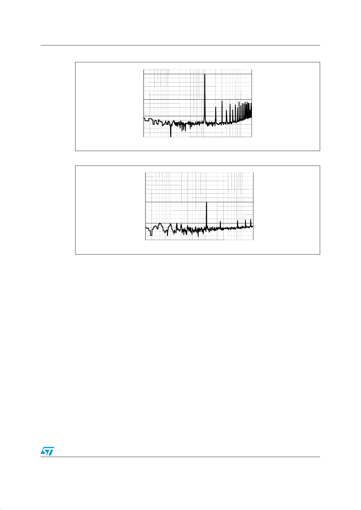
Figure 21. FFT (0 dB) . . . . . . . . . . . . . . . . . . . . . . . . . . . . . . . . . . . . . . . . . . . . . . . . . . . . . . . . . . . . . 22
Figure 22. FFT (-60 dB) . . . . . . . . . . . . . . . . . . . . . . . . . . . . . . . . . . . . . . . . . . . . . . . . . . . . . . . . . . . 22
Figure 23. THD vs output power at 1 kHz . . . . . . . . . . . . . . . . . . . . . . . . . . . . . . . . . . . . . . . . . . . . . . 23
Figure 24. THD vs output power at 100 Hz . . . . . . . . . . . . . . . . . . . . . . . . . . . . . . . . . . . . . . . . . . . . . 23
Figure 25. THD vs frequency at 100 mW . . . . . . . . . . . . . . . . . . . . . . . . . . . . . . . . . . . . . . . . . . . . . . 23
Figure 26. THD vs frequency at 1 W . . . . . . . . . . . . . . . . . . . . . . . . . . . . . . . . . . . . . . . . . . . . . . . . . . 24
Figure 27. Frequency response at 1 W . . . . . . . . . . . . . . . . . . . . . . . . . . . . . . . . . . . . . . . . . . . . . . . . 24
Figure 28. Crosstalk vs frequency at 1 W . . . . . . . . . . . . . . . . . . . . . . . . . . . . . . . . . . . . . . . . . . . . . . 24
Figure 29. FFT (0 dB) . . . . . . . . . . . . . . . . . . . . . . . . . . . . . . . . . . . . . . . . . . . . . . . . . . . . . . . . . . . . . 25
Figure 30. FFT (-60 dB) . . . . . . . . . . . . . . . . . . . . . . . . . . . . . . . . . . . . . . . . . . . . . . . . . . . . . . . . . . . 25
Figure 31. HTSSOP24 EPD outline . . . . . . . . . . . . . . . . . . . . . . . . . . . . . . . . . . . . . . . . . . . . . . . . . . 26
Doc ID 14570 Rev 6 3/30
Page 4

List of tables TDA7493
List of tables
Table 1. Device summary . . . . . . . . . . . . . . . . . . . . . . . . . . . . . . . . . . . . . . . . . . . . . . . . . . . . . . . . . . 1
Table 2. Pin list . . . . . . . . . . . . . . . . . . . . . . . . . . . . . . . . . . . . . . . . . . . . . . . . . . . . . . . . . . . . . . . . . . 7
Table 3. Absolute maximum rating . . . . . . . . . . . . . . . . . . . . . . . . . . . . . . . . . . . . . . . . . . . . . . . . . . . 9
Table 4. Thermal data. . . . . . . . . . . . . . . . . . . . . . . . . . . . . . . . . . . . . . . . . . . . . . . . . . . . . . . . . . . . . 9
Table 5. Electrical characteristics . . . . . . . . . . . . . . . . . . . . . . . . . . . . . . . . . . . . . . . . . . . . . . . . . . . . 9
Table 6. Mode selection . . . . . . . . . . . . . . . . . . . . . . . . . . . . . . . . . . . . . . . . . . . . . . . . . . . . . . . . . . 11
Table 7. Gain selection . . . . . . . . . . . . . . . . . . . . . . . . . . . . . . . . . . . . . . . . . . . . . . . . . . . . . . . . . . . 11
Table 8. Resistance values for input configuration . . . . . . . . . . . . . . . . . . . . . . . . . . . . . . . . . . . . . . 14
Table 9. Master and slave mode . . . . . . . . . . . . . . . . . . . . . . . . . . . . . . . . . . . . . . . . . . . . . . . . . . . 15
Table 10. HTSSOP24 EPD dimensions . . . . . . . . . . . . . . . . . . . . . . . . . . . . . . . . . . . . . . . . . . . . . . . 27
Table 11. Document revision history . . . . . . . . . . . . . . . . . . . . . . . . . . . . . . . . . . . . . . . . . . . . . . . . . 29
4/30 Doc ID 14570 Rev 6
Page 5
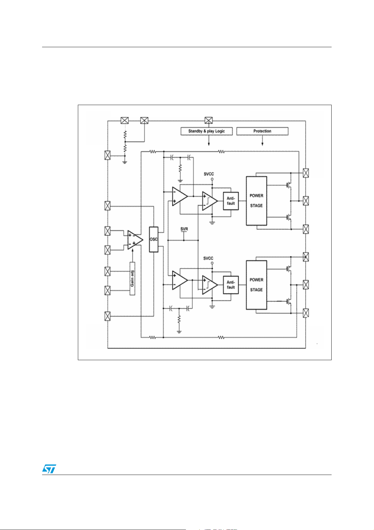
TDA7493 Device block diagram
1 Device block diagram
Figure 1 shows the block diagram of one of the two identical channels of the TDA7493.
Figure 1. TDA7493 block diagram (only one of two channels shown)
STANDBYSVRSVCC
SGND
PVCCP
ROSC
INP
INN
GAIN0
GAIN1
SYNCLK
OUTP
PGNDP
PVCCN
OUTN
PGNDN
Doc ID 14570 Rev 6 5/30
Page 6
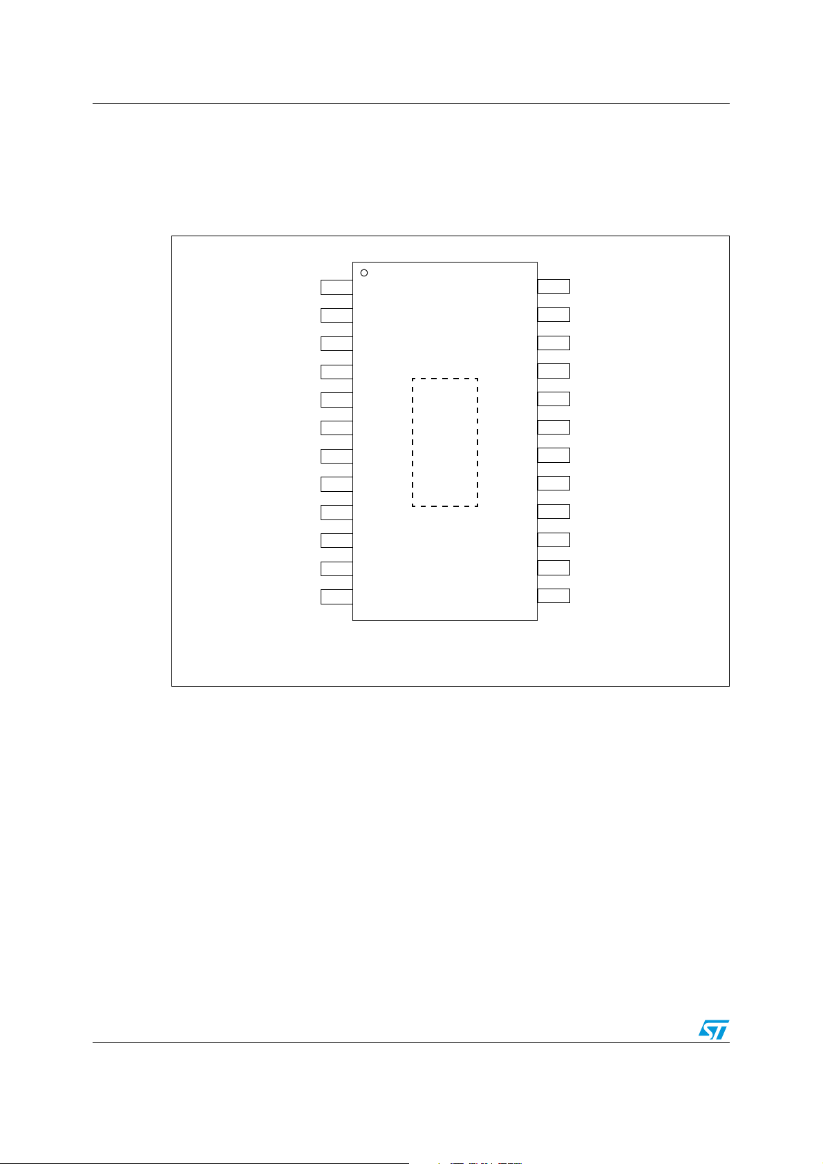
Pin description TDA7493
2 Pin description
2.1 Pin-out
Figure 2. Pin connection (top view)
SVR
24
23
22
21
20
19
18
17
16
15
14
13
1
INNL
2
INPL
3
STANDBY
4
PVCCPL
5
OUTPL
6
PGNDPL
7
PGNDNL
8
OUTNL
9
PVCCNL
10
SYNCLK
11
ROSC
12
SGND
The exposed pad is the device ground and must be connected appropriately
Exposed
pad (GND)
INNR
INPR
PVCCPR
OUTPR
PGNDPR
PGNDNR
OUTNR
PVCCNR
GAIN1
GAIN0
SVCC
6/30 Doc ID 14570 Rev 6
Page 7

TDA7493 Pin description
2.2 Pin list
Table 2. Pin list
Number Name Type Description
1 INNL IN Negative differential input of left channel
2 INPL IN Positive differential input of left channel
Standby mode control (digital):
3 STANDBY IN
4 PVCCPL POWER Power supply for positive branch in left channel
5 OUTPL OUT Positive PWM output for left channel
6 PGNDPL POWER Power stage ground for left channel
7 PGNDNL POWER Power stage ground for left channel
8 OUTNL OUT Negative PWM output for left channel
9 PVCCNL POWER Power supply for negative branch in left channel
10 SYNCLK IN/OUT Clock in/out for external oscillator
11 ROSC OUT Master oscillator frequency setting pin
12 SGND POWER Signal ground
13 SVCC POWER Signal power supply
0: standby
1: play
14 GAIN0 IN Gain setting input 1
15 GAIN1 IN Gain setting input 2
16 PVCCNR POWER Power supply for negative branch in right channel
17 OUTNR OUT Negative PWM output for right channel
18 PGNDNR POWER Power stage ground for right channel
19 PGNDPR POWER Power stage ground for right channel
20 OUTPR OUT Positive PWM output for right channel
21 PVCCPR POWER Power supply for positive branch in right channel
22 SVR OUTPUT Supply voltage rejection
23 INPR IN Positive differential input of right channel
24 INNR IN Negative differential input of right channel
Doc ID 14570 Rev 6 7/30
Page 8
8/30 Doc ID 14570 Rev 6
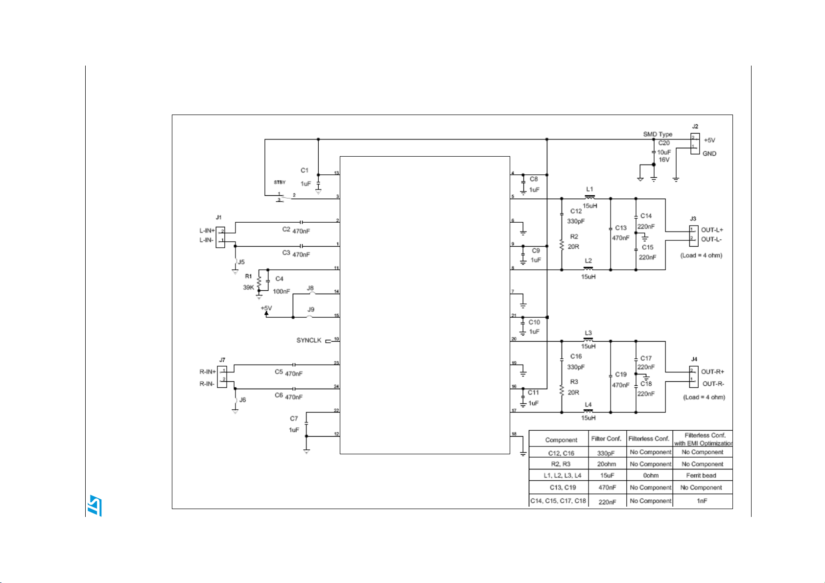
3 Applications circuit
Figure 3. Typical application circuit
Applications circuit TDA7493
Jumper 5 for
single-ended
input
Jumper 6 for
single-ended
input
SVCC
STANDBY
INPL
INNL
ROSC
GAIN0
GAIN1
SYNCLK
INPR
INNR
SVR
SGND
TDA7493
PVCCPL
OUTPL
PGNDPL
PVCCNL
OUTNL
PGNDNL
PVCCPR
OUTPR
PGNDPR
PVCCNR
OUTNR
PGNDNR
Page 9
TDA7493 Electrical specifications
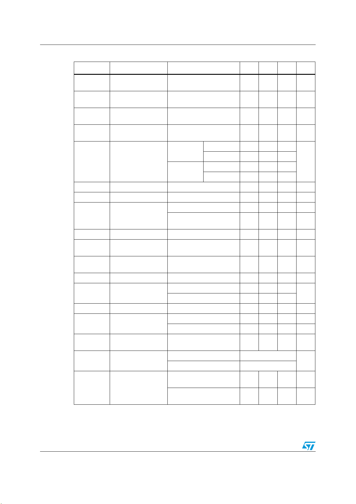
4 Electrical specifications
4.1 Absolute maximum ratings
Table 3. Absolute maximum rating
Symbol Parameter
V
CC
V
CC_STANDBY
Vi
DC supply on pins PVCCPL, PVCCPR, PVCCNL,
PVCCNR, SVCC
Standby DC supply on pins PVCCPL, PVCCPR,
PVCCNL, PVCCNR, SVCC
Input on pins STANDBY, INNL, INPL, INNR, INPR,
GAIN0, GAIN1
Top Operating temperature 0 70 °C
Tstg, Tj Storage and junction temperature -40 150 °C
4.2 Thermal data
Table 4. Thermal data
Symbol Parameter Min Typ Max Unit
Rth j-case Thermal resistance junction to case - 2 3 °C/W
Rth j-amb
1. FR4 with via holes, copper area 9 cm² as explained in Chapter 8 on page 28.
Thermal resistance junction to ambient
(on recommended PCB)
(1)
Negative
value
Positive
value
Unit
-0.3 6 V
-0.3 7 V
-0.3 6 V
-37-°C/W
4.3 Electrical characteristics
Refer to Figure 3: Typical application circuit, VCC = 5 V, RL (load) = 4 Ω, R1 = 39 kΩ,
C4 = 100 nF, f = 1 kHz, G
Table 5. Electrical characteristics
Symbol Parameter Condition Min Typ Max Unit
V
CC
Iq Total quiescent current No filter, no load - 7 - mA
Vos Output offset voltage Vi = 0, Gv = 6 dB, no load -20 - 20 mV
Po
Po
Supply range - 3.0 - 5.5 V
Output power
(filterless)
Output power (with
filter)
= 18 dB, Tamb = 25 °C, unless otherwise specified.
V
Doc ID 14570 Rev 6 9/30
THD = 10% - 3.0 - W
THD = 1% -2.4-W
THD = 10% - 2.8 - W
THD = 1% -2.2-W
Page 10
Electrical specifications TDA7493
Table 5. Electrical characteristics (continued)
Symbol Parameter Condition Min Typ Max Unit
Pd Dissipated power
η Efficiency
THD
Tj
Total harmonic
distortion
Thermal shut-down
junction temperature
Po = 2.8 W + 2.8 W,
THD = 10%
Po = 2.8 W + 2.8 W,
=4Ω
R
L
= 4 Ω, Po = 0.5 W - 0.05 - %
R
L
-1.1-W
-83-%
--150-°C
GAIN1 = low - 6.0 -
GAIN0 = low
GAIN1 = high - 12.0 -
G
V
Closed loop gain
GAIN1 = low - 15.6 -
dB
GAIN0 = high
GAIN1 = high - 18.0 -
GV Gain matching - -1 - 1 dB
CT Crosstalk f = 1 kHz - 60 - dB
A curve, Gv = 18 dB - 50 - µV
eN Total output noise
f = 22 Hz to 22 kHz,
Gv = 18 dB
-60-µV
Ri Input resistance Differential Input - 60 - k
SVRR
V
OVP
, t
t
r
f
R
DSON
f
SW
f
SWR
I
qSTANDBY
Supply voltage
rejection ratio
Overvoltage protection
threshold
Rising and falling time - - 10 - ns
Power transistor on
resistance
Switching frequency Internal oscillator - 315 - kHz
Output switching
frequency range
Quiescent current in
standby
f
= 100 Hz, Vr = 0.5 V,
C
r
SVR
=1µF
-55-dB
--5.8-V
High side - 0.44 -
Ω
Low side - 0.36 -
With internal oscillator
(1)
With external oscillator
--1-µA
250 - 400 kHz
(2)
250 - 400 kHz
Ω
Function
mode
Standby and play
STANDBY = high Play
STANDBY = low Standby
High
Digital inputs Digital input thresholds
Low - -
1. fSW = 106 / (R
f
= 2 * fSW with R1 = 39 kΩ and fSW in kHz
SYNC
= f
2. f
SW
SYNC
* 64 + 840)
OSC
/ 2 with the frequency of external oscillator
10/30 Doc ID 14570 Rev 6
0.7 *
V
CC
-
--V
0.3 *
V
CC
V
Page 11

TDA7493 Applications information
5 Applications information
5.1 Mode selection
Pin STANDBY selects the operating mode, namely standby or play.
z In standby mode, all the circuits are turned off and there is very low leakage current.
z In play mode, the amplifiers are powered up.
During the turn on/off sequence, there are four operational states: standby, pre-charge,
mute and play. The pre-charge and mute states are two internal transient states to set up
the normal operating condition and to reduce the speaker pop noise.
Table 6. Mode selection
Logic level on pin STANDBY Mode
0 Standby
1Play
Note: An internal pull-down resistor on pin STANDBY ensures that the default mode is standby.
5.2 Gain setting
The close loop gain is set by pins GAIN0 and GAIN1 as shown below in Ta bl e 7 . The gain
setting is implemented by changing the feedback resistors of the amplifiers.
Table 7. Gain selection
Logic level on pin GAIN0 Logic level on pin GAIN1 Gv (nominal)
006.0 dB
0 1 12.0 dB
1 0 15.6 dB
1 1 18.0 dB
Note: Internal pull-down resistors on pins GAIN0 and GAIN1 ensure that the default gain is 6 dB.
Doc ID 14570 Rev 6 11/30
Page 12

Applications information TDA7493
5.3 Input resistance and capacitance
The input impedance is set by an internal resistor, Ri, of value 60 kΩ. An input coupling
capacitor (Ci) is required on each input line. These two components together form a
high-pass filter whose cutoff frequency is:
f
= 1 / (2 * π * Ri * Ci)
C
Figure 4. Input high-pass RC filter
The value of Ci is chosen depending on the application and the speaker system. For a
cut-off frequency less than 20 Hz, the input capacitors could be 470 nF each.
If a polarized capacitor is used, it is important to connect the positive side of the capacitor to
the terminal with higher DC voltage. The DC voltage on the input pins is V
Figure 5. Device input structure
CC
/ 2.
Rf
Ci
Ri
+
Input signal
-
Ci
Ri
Rf
12/30 Doc ID 14570 Rev 6
Page 13

TDA7493 Applications information
5.4 Filterless modulation
The modulation scheme of BTL is called unipolar PWM output. The differential output
voltage changes between zero and +V
traditional bipolar PWM output between +V
scheme effectively doubles the switching frequency of the differential output waveform.
Signals on OUTP and OUTN are in the same phase when the input is zero, thus the current
is greatly reduced and the loss in the load is small. A tiny delay between OUTP and OUTN is
introduced to avoid high transient currents which could occur if both outputs switch
simultaneously.
TDA7493 can be used without a filter between the PWM output and the speaker since the
switching frequency of the output is beyond the audible range. The audio signal can be
recovered by the inherent inductance of the speaker and natural filter of the human ear.
Figure 6. Unipolar PWM output
or between zero and -VCC, as opposed to the
CC
and -VCC. The other advantage of this
CC
The filterless configuration is usable in applications where the speaker connections to the
amplifier are shorter than 50 cm. In comparison to the low-pass Butterworth filter
configuration, the filterless configuration gives rise to higher EMI. This can be reduced, if
necessary, by inserting a ferrite bead filters close to the device.
Use a ferrite which exhibits high impedance at around 1 MHz and negligible impedance in
the audio band.
It is recommended to use an EMI filter if the speaker cable is longer than 50 cm.
Doc ID 14570 Rev 6 13/30
Page 14

14/30 Doc ID 14570 Rev 6
Figure 7. Schematic for the filterless configuration
Applications information TDA7493
8
8
Table 8. Resistance values for input configuration
SVCC
STANDBY
INPL
INNL
ROSC
GAIN0
GAIN1
SYNCLK
INPR
INNR
SVR
SGND
TDA7493
PVCCPL
OUTPL
PGNDPL
PVCCNL
OUTNL
PGNDNL
PVCCPR
OUTPR
PGNDPR
PVCCNR
OUTNR
PGNDNR
(*1) R2, R3, R4 and R5 are 0-Ω resistors which can be replaced
by ferrite beads if EMI optimization is required
(*2) C14, C15, C17, and C18 are 1-nF capacitors which are needed
when ferrite beads are used for EMI optimization
TDA7493 amplifier (filterless)
Page 15

TDA7493 Applications information
5.5 Internal clock and external clock
The clock of the class-D amplifier can be generated internally or it can be synchronous with
the external clock. If two or more class-D amplifiers are used in the same system, it is better
to have all devices working at the same frequency. This is realized by using one TDA7493
as clock master and the others as slaves. All SYNCLK pins are connected together as
shown in Figure 8.
In master mode or with a single TDA7493, the output switching frequency is controlled by
the resistor connected to pin ROSC. The switching frequency is:
f
Note: R
= 106 / (R
SW
where R
is in kΩ and fSW is in kHz.
OSC
In this configuration pin SYNCLK is an output whose frequency is also determined by R
f
SYNCLK
should be lower than 60 kΩ in master mode to avoid operating in error mode.
OSC
= 106 / (R
In slave mode, pin ROSC can be floating to force pin SYNCLK as input in order to accept the
master clock. The switching frequency in this mode is:
f
= f
SW
SYNCLK
Table 9. Master and slave mode
* 64 + 840)
OSC
OSC
/ 2
OSC
* 32 + 420) = 2 * fSW
:
Mode Pin ROSC Pin SYNCLK
Master R
< 60 kΩ Output
OSC
Slave Floating Input
Figure 8. Master and slave modes
Master
TDA7493
SYNCLK ROSC
Input
C
OSC
100 nF
ROSC
SYNCLK
R
OSC
39 kΩ
Output
Slave
TDA7493
Doc ID 14570 Rev 6 15/30
Page 16

Applications information TDA7493
5.6 Output low-pass filter
To avoid EMI problems, a low-pass filter can be inserted before the speaker. The cut-off
frequency of the filter should be higher than 22 kHz and much lower than the switching
frequency.
The component values of the filter vary according to the speaker impedance.
A typical LC output filter for a speaker impedance of 8 Ω and with a cut-off frequency of
27 kHz is shown in Figure 9.
Figure 9. Typical LC filter for 8 Ω speaker
OUTP
33 µH
330 pF
0.10 µF
20 Ω
33 µH
OUTN
A similar filter for a speaker impedance of 4 Ω and also with a cut-off frequency of 27 kHz is
shown in Figure 10:
Figure 10. Typical LC filter for 4 Ω speaker
OUTP
15 µH
330 pF
20 Ω
15 µH
OUTN
0.47 µF
8 Ω
0.10 µF
0.22 µF
0.47 µF
4 Ω
0.22 µF
16/30 Doc ID 14570 Rev 6
Page 17

TDA7493 Applications information
5.7 Protection function
The TDA7493 has four types of protection: overvoltage (OV), undervoltage (UV), thermal
(OT) and short circuit (SC):
z overvoltage protection (OVP) for the supply V
z undervoltage protection (UVP) for the supply V
z thermal protection (OTP) for the junction temperature Tj > 155 °C
z short-circuit protection (SCP) across the load (tested at V
CC
CC
> 6 V
< 3 V
= 5.0 V).
CC
When any of the above protection becomes active, the output goes to a high-impedance
state. The device remains in this state until the condition is cleared or rectified, when the
circuit restarts again.
5.8 Differential input
The TDA7493 can be used with either differential or single-ended inputs. In either case, the
device must be AC coupled to the audio source.
To use the device with a differential source, connect the positive lead from the audio source
to the INP input and the negative lead to the INN input as shown in Figure 11. The
differential input stage of the amplifier minimizes the common mode noise effectively.
In the differential input application:
z input impedance is given by 2 * Rin,
z cut-off frequency of the input filter is given by
f
= 1 / (2 * π * Cin / 2 * 2 * Rin) = 1 / (2 * π * Cin * Rin).
c
Typically, Rin = 30 k
Ω and Cin > 330 nF to get a cut-off frequency
Figure 11. Differential input application
OUTP
OUTN
Audio Source
Cin
Cin
INP
INN
TDA7493
Rin
Rin
Input stage
less than 20 Hz.
Rfb
+
-
Rfb
Doc ID 14570 Rev 6 17/30
Page 18

Applications information TDA7493
5.8.1 Single-ended input application
To use the device with a single-ended source, one input is AC connected to ground (via a
capacitor) and the other input is connected to the audio source. This is designed as a fully
differential input. The input scheme is shown in Figure 12.
However, to avoid the start-up pop noise, it is important to equalize, as much as possible,
the charging currents in the positive and negative inputs. Any imbalance in these charging
currents will be amplified and result in the familiar turn-on pop.
Figure 12. Single-ended input application
Cin
OUTP INP
cin
TDA7493
Rfb
+
Rin
Cin
Audio Source
GND
cin
INN
Rin
-
Rfb
Input stage
Since the input charging currents in the circuit of Figure 12 can be different it is necessary to
add two resistors, R0, as shown in the circuit of Figure 13. In this way the currents in the two
branches of the differential input are better balanced and this can lead to the elimination of
the turn-on pop noise.
Figure 13. Anti-pop configuration for single-ended input application
TDA7493
OUTP INP
R0
GND
Audio Source
R0
Cin
Cin
18/30 Doc ID 14570 Rev 6
INN
Rin
Rin
Rfb
+
-
Rfb
Input stage
Page 19

TDA7493 Applications information
The disadvantages of the anti-pop configuration are given below:
z The input impedance or the load of audio source is no longer 2 * Rin as in the case of
differential input configuration but R0. It means the load effect should be considered
during the application design. At this point, bigger R0 is better because of the lower
load effect.
z The input signal is also equivalent to
V
in_actual
the original V
When Rin = 30 k
When Rin = 30 k
= Vin * 2 * Rin * (Rin + Rfb + R0) / (2 * Rin * (Rin + Rfb + R0) + Rfb * R0), not
which means the actual gain is reduced.
in
Ω, Rfb = 30 kΩ and R0 = 20 kΩ, the gain is reduced by 1 dB.
Ω, Rfb = 120 kΩ and R0 = 20 kΩ, the gain is reduced by 1.84 dB. In
this case, smaller R0 is better.
If the pop noise is not critical, the anti-pop configuration can be simplified as shown in
Figure 14. The suggested value of the resistor R0 is 20 k
Ω.
Figure 14. Simple anti-pop configuration for single-ended input application
TDA7493
Rfb
R0
Cin
Cin
INN
Rin
Rin
+
-
OUTP INP
GND
Audio Source
Rfb
Input stage
Doc ID 14570 Rev 6 19/30
Page 20

Electrical characterization curves TDA7493
6 Electrical characterization curves
6.1 For the configuration with LC filter
z Test setup as given in Figure 3 on page 8
z Test conditions V
Figure 15. THD vs output power at 1 kHz
d
B
r
A
= 5 V, C20 = 10 µF, RL = 4 Ω, LC filter 15 µH, 470 nF
CC
10
THD
5
(%)
2
1
0.5
0.2
0.1
0.05
0.02
0.01
0.005
0.002
0.001
100m 3200m 300m 400m 500m 700m 1 2
Po (W)
Figure 16. THD vs output power at 100 Hz
10
THD
5
(%)
2
1
0.5
0.2
0.1
0.05
0.02
0.01
0.005
0.002
0.001
100m
Po (W)
Figure 17. THD vs frequency at 100 mW
10
THD
5
(%)
2
1
0.5
0.2
0.1
0.05
0.02
0.01
20 20k50 100 200 500 1k 2k 5k 10k
3200m 300m 400m 500m 700m 1 2
Frequency
20/30 Doc ID 14570 Rev 6
Page 21

TDA7493 Electrical characterization curves
Figure 18. THD vs frequency at 1 W
10
THD
5
(%)
2
1
0.5
0.2
0.1
0.05
0.02
0.01
0.005
0.002
0.001
20 20k50 100 200 500 1k 2k 5k 10k
Frequency
Figure 19. Output frequency response at 1 W
+2
Ampl
+1
(dB)
-0
-1
-2
-3
-4
-5
20 50k50 100 200 500 1k 2k 5k 10k 20k
Frequency (Hz)
Figure 20. Crosstalk vs frequency at 1 W
Crosstalk
(dB)
+0
-10
-20
-30
-40
-50
-60
-70
-80
-90
-100
-110
-120
20 20k50 100 200 500 1k 2k 5k 10k
TTTTTTT
Frequency (Hz)
Doc ID 14570 Rev 6 21/30
Page 22

Electrical characterization curves TDA7493
Figure 21. FFT (0 dB)
+10
FFT
+0
-10
(dB)
-20
-30
-40
-50
-60
-70
-80
-90
-100
-110
-120
-130
-140
-150
20 20k50 100 200 500 1k 2k 5k 10k
Frequency (Hz)
Figure 22. FFT (-60 dB)
+10
FFT
+0
-10
(dB)
-20
-30
-40
-50
-60
-70
-80
-90
-100
-110
-120
-130
-140
-150
20 20k50 100 200 500 1k 2k 5k 10k
Frequency (Hz)
22/30 Doc ID 14570 Rev 6
Page 23

TDA7493 Electrical characterization curves
6.2 For the configuration without filter
z Test setup as given in Figure 7 on page 14
z Test conditions V
Figure 23. THD vs output power at 1 kHz
Figure 24. THD vs output power at 100 Hz
= 5 V, C20 = 10 µF, RL = 4 Ω + 270 µH, no LC filter
CC
10
THD
5
(%)
2
1
0.5
0.2
0.1
0.05
0.02
0.01
100m 4200m 300m 400m 600m 800m 1 2 3
Po (W)
10
THD
5
(%)
2
1
0.5
0.2
0.1
0.05
0.02
0.01
100m 4200m 300m 400m 600m 800m 1 2 3
Po (W)
Figure 25. THD vs frequency at 100 mW
10
THD
5
(%)
2
1
0.5
0.2
0.1
0.05
0.02
0.01
0.005
0.002
0.001
20 20k50 100 200 500 1k 2k 5k 10k
Doc ID 14570 Rev 6 23/30
frequency (Hz)
Page 24

Electrical characterization curves TDA7493
Figure 26. THD vs frequency at 1 W
10
THD
5
(%)
2
1
0.5
0.2
0.1
0.05
0.02
0.01
0.005
0.002
0.001
20 20k50 100 200 500 1k 2k 5k 10k
frequency (Hz)
Figure 27. Frequency response at 1 W
+2
Ampl
(dB)
+1
-0
-1
-2
-3
-4
-5
20 50k50 100 200 500 1k 2k 5k 10k 20k
frequency (Hz)
Figure 28. Crosstalk vs frequency at 1 W
TTTTTTT
Crosstalk
(dB)
+40
+20
+0
-20
-40
-60
-80
-100
-120
-140
20 20k50 100 200 500 1k 2k 5k 10k
frequency (Hz)
24/30 Doc ID 14570 Rev 6
Page 25
TDA7493 Electrical characterization curves
Figure 29. FFT (0 dB)
+10
FFT
+0
(dB)
-10
-20
-30
-40
-50
-60
-70
-80
-90
-100
-110
-120
-130
-140
-150
20 20k50 100 200 500 1k 2k 5k 10k
frequency (Hz)
Figure 30. FFT (-60 dB)
+10
+0
FFT
-10
(dB)
-20
-30
-40
-50
-60
-70
-80
-90
-100
-110
-120
-130
-140
-150
20 20k50 100 200 500 1k 2k 5k 10k
frequency (Hz)
Doc ID 14570 Rev 6 25/30
Page 26

Package mechanical data TDA7493
7 Package mechanical data
The TDA7493 comes in a 24-pin HTSSOP exposed-pad-down package. The outline is
shown in Figure 31 and the dimensions are given in Ta bl e 1 0.
The package code is YO and the JEDEC/EIAJ reference number is JEDEC MO-153-ADT.
Figure 31. HTSSOP24 EPD outline
26/30 Doc ID 14570 Rev 6
Page 27

TDA7493 Package mechanical data
Table 10. HTSSOP24 EPD dimensions
mm inch
Reference
Min Typ Max Min Typ Max
A--1.20--0.047-
A1 - - 0.15 - - 0.006 -
A2 0.80 1.00 1.05 0.031 0.039 0.041 -
b 0.19 - 0.30 0.007 - 0.012 -
c 0.09 - 0.20 0.004 - 0.008 -
D 7.70 7.80 7.90 0.303 0.307 0.311
D1 4.80 5.00 5.2 0.189 0.197 0.205 -
E 6.20 6.40 6.60 0.244 0.252 0.260 -
E1 4.30 4.40 4.50 0.169 0.173 0.177
E2 3.00 3.20 3.40 0.118 0.126 0.134 -
e - 0.65 - - 0.026 - -
L 0.45 0.60 0.75 0.018 0.024 0.030 -
L1 - 1.00 - - 0.039 - -
aaa - - 0.10 - - 0.004 -
Notes
(1)
(2)
k0-80-8degrees
1. Dimension D does not include mold flash, protrusions or gate burrs. Mold flash, protrusions or gate burrs
shall not exceed 0.15mm (0.006 inch) per side.
2. Dimension E1 does not include interlead flash or protrusions. Interlead flash or protrusions does not
exceed 0.25mm (0.010 inch) per side.
In order to meet environmental requirements, ST offers these devices in different grades of
ECOPACK
specifications, grade definitions and product status are available at: www.st.com.
ECOPACK
®
packages, depending on their level of environmental compliance. ECOPACK®
®
is an ST trademark.
Doc ID 14570 Rev 6 27/30
Page 28

Heatsink provision TDA7493
8 Heatsink provision
With the exposed-pad packages, it is possible to use the printed circuit board as a heatsink.
Using a PCB copper ground area of 3 x 3 cm
exposed pad, a thermal resistance of 37 °C/W can be achieved.
The amount of power dissipated within the device depends primarily on the supply voltage,
load impedance and output modulation level. The maximum estimated power dissipation for
the TDA7493 is around 1.1 W.
With the suggested copper area of 9 cm
than 40 °C above ambient can be expected, thus giving a maximum junction temperature,
Tj, of approximately 90 °C in consumer environments where 50 °C is specified as the
maximum ambient temperature. This provides a comfortable safety margin to the thermal
protection threshold at Tj = 150 °C.
2
with 16 via holes to make contact with the
2
, a maximum junction temperature increase of less
28/30 Doc ID 14570 Rev 6
Page 29

TDA7493 Revision history
9 Revision history
Table 11. Document revision history
Date Revision Changes
02-Apr-2008 1 Initial release.
Updated application schematic on page 8
Updated Table 5: Electrical characteristics on page 9
16-Sep-2008 2
Updated schematic of input structure on page 12
Updated Schematic for the filterless configuration on page 14
Updated section 5.8: Differential input on page 17.
01-Dec-2008 3
Added test voltage note to SC protection in section 5.7: Protection
function on page 17.
Replaced 2.8 W with 3 W in title on page 1
Added new feature of 3.0 W on on page 1
Updated description for pin STANDBY in Table 2: Pin list on page 7
14-Dec-2008 4
Added output power for filterless config to Table 5: Electrical
characteristics on page 9
Updated values for digital input thresholds in Table 5: Electrical
characteristics on page 9
Updated text for environmentally-friendly packaging on page 27.
14-Oct-2009 5
Updated minimum operating voltage on page 1 and on page 9
Updated formula for f
29-Nov-2010 6 Added V
CC_STANDBY
on page 10 and on page 15.
SW
to Table 3: Absolute maximum rating on page 9
Doc ID 14570 Rev 6 29/30
Page 30

TDA7493
Please Read Carefully:
Information in this document is provided solely in connection with ST products. STMicroelectronics NV and its subsidiaries (“ST”) reserve the
right to make changes, corrections, modifications or improvements, to this document, and the products and services described herein at any
time, without notice.
All ST products are sold pursuant to ST’s terms and conditions of sale.
Purchasers are solely responsible for the choice, selection and use of the ST products and services described herein, and ST assumes no
liability whatsoever relating to the choice, selection or use of the ST products and services described herein.
No license, express or implied, by estoppel or otherwise, to any intellectual property rights is granted under this document. If any part of this
document refers to any third party products or services it shall not be deemed a license grant by ST for the use of such third party products
or services, or any intellectual property contained therein or considered as a warranty covering the use in any manner whatsoever of such
third party products or services or any intellectual property contained therein.
UNLESS OTHERWISE SET FORTH IN ST’S TERMS AND CONDITIONS OF SALE ST DISCLAIMS ANY EXPRESS OR IMPLIED
WARRANTY WITH RESPECT TO THE USE AND/OR SALE OF ST PRODUCTS INCLUDING WITHOUT LIMITATION IMPLIED
WARRANTIES OF MERCHANTABILITY, FITNESS FOR A PARTICULAR PURPOSE (AND THEIR EQUIVALENTS UNDER THE LAWS
OF ANY JURISDICTION), OR INFRINGEMENT OF ANY PATENT, COPYRIGHT OR OTHER INTELLECTUAL PROPERTY RIGHT.
UNLESS EXPRESSLY APPROVED IN WRITING BY AN AUTHORIZED ST REPRESENTATIVE, ST PRODUCTS ARE NOT
RECOMMENDED, AUTHORIZED OR WARRANTED FOR USE IN MILITARY, AIR CRAFT, SPACE, LIFE SAVING, OR LIFE SUSTAINING
APPLICATIONS, NOR IN PRODUCTS OR SYSTEMS WHERE FAILURE OR MALFUNCTION MAY RESULT IN PERSONAL INJURY,
DEATH, OR SEVERE PROPERTY OR ENVIRONMENTAL DAMAGE. ST PRODUCTS WHICH ARE NOT SPECIFIED AS "AUTOMOTIVE
GRADE" MAY ONLY BE USED IN AUTOMOTIVE APPLICATIONS AT USER’S OWN RISK.
Resale of ST products with provisions different from the statements and/or technical features set forth in this document shall immediately void
any warranty granted by ST for the ST product or service described herein and shall not create or extend in any manner whatsoever, any
liability of ST.
ST and the ST logo are trademarks or registered trademarks of ST in various countries.
Information in this document supersedes and replaces all information previously supplied.
The ST logo is a registered trademark of STMicroelectronics. All other names are the property of their respective owners.
© 2010 STMicroelectronics - All rights reserved
STMicroelectronics group of companies
Australia - Belgium - Brazil - Canada - China - Czech Republic - Finland - France - Germany - Hong Kong - India - Israel - Italy - Japan -
Malaysia - Malta - Morocco - Philippines - Singapore - Spain - Sweden - Switzerland - United Kingdom - United States of America
www.st.com
30/30 Doc ID 14570 Rev 6
 Loading...