

Single chip RDS demodulator + filter
Features
■ Very high RDS demodulation quality with
improved digital signal processing
■ High performance, 57 kHz bandpass filter
th
(8
order)
■ FIlter adjustment free and without external
components
■ Purely digitaL RDS Demodulation without
external components
■ ARI (SK indication) and RDS signal quality
output
■ 4.332 MHz crystal oscillator
(8.664 and 17.328 MHz optional)
■ Low noise CMOS technology
■ Low radiation
Description
The TDA7479 recovers the additional inaudible
RDS information which is transmitted by FM radio
broadcasting stations and operates in accordance
with the EBU (European Broadcasting Union)
specifications.
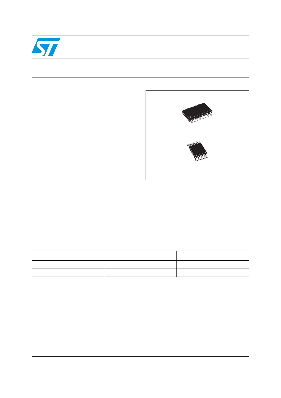
Table 1. Device summary
TDA7479
SO16
TSSOP16
The device is made up of two sections: a
cascaded antialiasing + switched capacitors 8
bandpass filter for precise RDS band selection
and a demodulating section that performs the
extraction od RDS data stream (RDDA) and clock
(RDCL), to be further processed by a suitable
RDS decoder.
Outputs for RDS signal quality and ARI indication
are also present.
th
Order code Package Packing
E-TDA7479D
E-TDA7479AD
1. Device in ECOPACK® package (see Section 5: Package information on page 9).
November 2008 Rev 7 1/12
(1)
(1)
SO16 Tube
TSSOP16 Tube
www.st.com
12

Contents TDA7479
Contents
1 Block diagram and pin description . . . . . . . . . . . . . . . . . . . . . . . . . . . . . 3
1.1 Block diagram . . . . . . . . . . . . . . . . . . . . . . . . . . . . . . . . . . . . . . . . . . . . . . . 3
1.2 Pin description . . . . . . . . . . . . . . . . . . . . . . . . . . . . . . . . . . . . . . . . . . . . . . 3
2 Electrical specification . . . . . . . . . . . . . . . . . . . . . . . . . . . . . . . . . . . . . . . 5
2.1 Thermal data . . . . . . . . . . . . . . . . . . . . . . . . . . . . . . . . . . . . . . . . . . . . . . . 5
2.2 Absolute maximum ratings . . . . . . . . . . . . . . . . . . . . . . . . . . . . . . . . . . . . . 5
2.3 Electrical characteristics . . . . . . . . . . . . . . . . . . . . . . . . . . . . . . . . . . . . . . . 5
3 Output timing . . . . . . . . . . . . . . . . . . . . . . . . . . . . . . . . . . . . . . . . . . . . . . . 7
4 Oscillator controls (FSEL, OSEL) . . . . . . . . . . . . . . . . . . . . . . . . . . . . . . 8
5 Package information . . . . . . . . . . . . . . . . . . . . . . . . . . . . . . . . . . . . . . . . . 9
6 Revision history . . . . . . . . . . . . . . . . . . . . . . . . . . . . . . . . . . . . . . . . . . . 11
2/12
TDA7479 Block diagram and pin description
1 Block diagram and pin description
1.1 Block diagram
Figure 1. Block diagram
4.332MHz C2 47pFC1 27pF
MPX
V
S
100nF
10μF
270pF
FILOUT
4
8
12
3VREF
GND
2nd ORDER
ANTIALIASING
FILTER
8th ORDER
SC-BANDPASS
FILTER
-
+
6
1.2 Pin description
T57
15
57KHz PLL
FAST ARI
INDICATOR
POLARITY
BIPHASE DEC.
INTEGRAL
BIPHASE DEC.
OSCILLATOR &
DIVIDER
OSCOUTOSCIN
1413
5
OSEL
9
FSEL
16
1187.5Hz
PLL
QUAL DET.
0
MUX
1
EXTRES
DIFF. DECODER
TEST LOGIC
11
D97AU751A
RDCL
7
ARI
1
QUAL
2
RDDA
10
TM
Figure 2. Pin connection (top view)
QUAL
RDDA
VREF
MPX
OSEL
GND
ARI
FILOUT 8 FSEL9
1
2
3
4
5
6
7TM
D97AU752
15
14
13
12
11
10
RDCL16
T57
OSCOUT
OSCIN
V
S
EXTRES
3/12
Block diagram and pin description TDA7479
Table 2. Pin description
No pin Name Description
1 QUAL Output for signal quality indication (High = good)
2 RDDA RDS data output
3 VREF Reference voltage
4 MPX RDS input signal
Oscillator selector pin:
5 OSEL
6 GND Ground
7ARI
8 FILOUT Filter output
9 FSEL
10 TM
– open, closed to V
= quartz oscillator
S
– closed to GND = external driven
Output for ARI indication:
– high when RDS+ARI are present
– high when only ARI is present
– low when only RDS is present
– undefined when nos signal is present
Frequency selector pin:
– 100 kHz to VS = 17.328 MHz
– open = 4.332MHz
– closed to VS = 8.664 MHz
Test mode pin:
– open = normal operation
– closed to VS = test mode
Reset pin:
11 EXTRES
– open = run mode
– -closed to VS = reset condition
12 V
S
Supply voltage
13 OSCIN Oscillator input
14 OSCOUT Oscillator output
15 T57 Testing output pin: 57 kHz clock output
16 RDCL RDS clock output 1187.5 Hz
4/12

TDA7479 Electrical specification
2 Electrical specification
2.1 Thermal data
Table 3. Thermal data
Symbol Parameter SO16 TSSOP16 Unit
R
th j-case
Thermal resistance junction to case Max. 200 160 °C/W
2.2 Absolute maximum ratings
Table 4. Absolute maximum ratings
Symbol Parameter Value Unit
V
T
T
Supply voltage -0.3 to 7 V
S
Operating temperature range -40 to 85 °C
op
Storage temperature -55 to 150 °C
stg
2.3 Electrical characteristics
Table 5. Electrical characteristics
Symbol Parameter Test condition Min. Typ. Max. Unit
V
S
I
S
Filter
(T
= 25°C, VS = 5V, unless otherwise specified)
amb
Supply voltage 4.5 5 5.5 V
Supply current 7.5 11.0 mA
f
Center frequency 56.5 57 57.5 kHz
C
BW 3dB Bandwidth 2.5 3 3.5 kHz
G Gain f = 57 kHz 18 20 22 dB
Δf ± 4 kHz 18 22 dB
A Attenuation
f = 38 kHz 50 60 dB
f = 67 kHz 35 45 dB
Input impedance of MPX 80 120 150 KΩ
R
I
Load impedance on FILOUT 1 MΩ
R
L
S/N Signal to noise ratio V
V
S
S
MPX input signal
IN
RDS detection sensitivity 1 mVrms
RDS
ARI Detection Sensitivity 3 mVrms
ARI
= 3 mVrms 30 40 dB
IN
f = 19 kHz; T3 ≤ 40 dB
(1)
100050mV
f = 57 kHz (RDS+ ARI)
mV
5/12
RMS
RMS

Electrical specification TDA7479
Table 5. Electrical characteristics (continued)
(T
= 25°C, VS = 5V, unless otherwise specified)
amb
Symbol Parameter Test condition Min. Typ. Max. Unit
V
Reference VS/2 V
REF
Demodulator
Input pins (EXTRES, FSEL, TM:) all with internal pull down resistor
Input pin (OSEL): with internal pull up resistor
I
I
V
V
Input current VIN = 5 V (pull-down input) 15 30 μA
PD
Input current VIN = 0 V (pull-up input) -25 -10 μA
PU
Input voltage high
IH
Input voltage low
IL
0.7 · VS0.8 · V
Output pins (RDCL, RDDA, ARI, QUAL, T57)
V
V
Output voltage high IL = 0.5mA 4 4.6 V
OH
Output voltage low IL = 0.5mA 0.4 1 V
OL
Oscillator
V
Input level OSCIN pin OSEL = open circuit 1 V
CLL
Input level OSCIN pin OSEL = open circuit 4 V
V
CLH
Amplitude OSCOUT OSEL = open circuit 4.5 V
OSEL = GND, f = 4.332 MHz
V
Amplitude OSCIN
PP
(for external drive)
OSEL = GND, f = 8.664 MHz
OSEL = GND, f = 17.328 MHz 150 mVpp
1. The 3rd harmonic (57 kHz) must be less than -40 dB with respect to the input signal plus gain.
S
0.2 · VS0.3 · V
100
120
S
V
V
mVpp
mVpp
6/12

TDA7479 Output timing
3 Output timing
The RDS (1187.5Hz) output clock on RDCL line is synchronized to the incoming data. According
to the internal PLL lock condition data change can result on the falling or on the rising clock edge
(see Figure 3). Whichever clock edge is used by the decoder (rising or falling edge) the data will
remain valid for 416.7
Figure 3. RDS timing diagram
µ
s after the clock transition.
RDCL
RDDA
4.3µs
td
CLOCK
LINE
DATA
LINE
4.3µs837.7µs 421µs 421µs
7/12

Oscillator controls (FSEL, OSEL) TDA7479
4 Oscillator controls (FSEL, OSEL)
Three different crystal frequencies can be used. The adoption of the internal clock divider to
the external crystal is achieved via the input pin FSEL. See the following table for reference:
Table 6. Crystal frequencies
Crystal FSEL (pin configuration)
4.332MHz
8.664MHz
17.328MHz
A special mode is introduced to reduce EMI. With pin OSEL connected to GND the internal
oscillator is switched off and an external sinusoidal frequency could be applied on OSCIN.
The peak to peak voltage of this signal can be reduced down to 60mV.
In this mode the frequency selection via FSEL is still active.
Suggested values of C1 and C2 are shown in the following table:
Table 7. C1 and C2 value
connected to GND or open connected to Vs external resistor of 100K to Vs
Crystal C1 C2
4.332MHz
8.664MHz
17.328MHz
27pF
27pF
27pF
47pF
-
-
8/12

TDA7479 Package information
5 Package information
In order to meet environmental requirements, ST (also) offers these devices in ECOPACK®
packages. ECOPACK
®
packages are lead-free. The category of second Level Interconnect
is marked on the package and on the inner box label, in compliance with JEDEC Standard
JESD97. The maximum ratings related to soldering conditions are also marked on the inner
box label.
ECOPACK is an ST trademark. ECOPACK specifications are available at: www.st.com.
Figure 4. SO16 mechanical data and package dimensions
DIM.
A 2.35 2.65 0.093 0.104
A1 0.10 0.30 0.004 0.012
B 0.33 0.51 0.013 0.200
C 0.23 0.32 0.009 0.013
(1)
D
E 7.40 7.60 0.291 0.299
e 1.27 0 .050
H 10.0 10.65 0.394 0.419
h 0.25 0.75 0.010 0.030
L 0.40 1.27 0.016 0.050
k 0˚ (min.), 8˚ (max.)
ddd 0.10 0.0 04
(1) “D” dimensio n does not include mold flash, prot usions or gate
burrs. Mol d flash, prot usions or gat e burrs shal l not exceed
0.15mm per sid e.
mm inch
MIN. TYP. MAX. MIN. TYP. MAX.
10.10 10.50 0.398 0.413
OUTLINE AND
MECHANICAL DATA
SO16 (Wide)
0016021 C
9/12

Package information TDA7479
Figure 5. TSSOP16 mechanical data and package dimensions
DIM.
A 1.200 0.047
A1 0.050 0.150 0.002 0.006
A2 0.800 1.000 1.050 0.031 0.039 0.041
b 0.190 0.300 0.007 0.012
c 0.090 0.200 0.005 0.009
D (1) 4.900 5.000 5.100 0.114 0.118 0.122
E 6.200 6.400 6.600 0.244 0 .252 0.260
E1 (1) 4.300 4.400 4.500 0.170 0 .173 0.177
e 0.650 0.026
L 0.450 0.600 0.750 0.018 0.024 0.0 30
L1 1.0 00 0 .039
k 0˚ (min.) 8˚ (max.)
aaa 0.100 0.004
Note: 1. D and E1 does not include mold flash or protrusions.
mm inch
MIN. TYP. MAX. MIN. TYP. MAX.
Mold flash or potrusions shall not exceed 0.15mm
(.006inch) p er side.
OUTLINE AND
MECHANICAL DATA
TSSOP16
(Body 4.4mm)
10/12
0080338 (Jedec MO-153-AB)

TDA7479 Revision history
6 Revision history
Table 8. Document revision history
Date Revision Changes
10-Sep-2004 4 Initial release.
20-Nov-2004 5
02-Dec-2004 6 Modified the order codes table.
04-Nov-2008 7
Add in Table 5: Electrical characteristics on page 5 the “RDS and
ARI Detection Sensitivity” parameters.
Document reformatted.
Updated Table 1: Device summary on page 1.
Updated Section 5: Package information on page 9.
11/12

TDA7479
Please Read Carefully:
Information in this document is provided solely in connection with ST products. STMicroelectronics NV and its subsidiaries (“ST”) reserve the
right to make changes, corrections, modifications or improvements, to this document, and the products and services described herein at any
time, without notice.
All ST products are sold pursuant to ST’s terms and conditions of sale.
Purchasers are solely responsible for the choice, selection and use of the ST products and services described herein, and ST assumes no
liability whatsoever relating to the choice, selection or use of the ST products and services described herein.
No license, express or implied, by estoppel or otherwise, to any intellectual property rights is granted under this document. If any part of this
document refers to any third party products or services it shall not be deemed a license grant by ST for the use of such third party products
or services, or any intellectual property contained therein or considered as a warranty covering the use in any manner whatsoever of such
third party products or services or any intellectual property contained therein.
UNLESS OTHERWISE SET FORTH IN ST’S TERMS AND CONDITIONS OF SALE ST DISCLAIMS ANY EXPRESS OR IMPLIED
WARRANTY WITH RESPECT TO THE USE AND/OR SALE OF ST PRODUCTS INCLUDING WITHOUT LIMITATION IMPLIED
WARRANTIES OF MERCHANTABILITY, FITNESS FOR A PARTICULAR PURPOSE (AND THEIR EQUIVALENTS UNDER THE LAWS
OF ANY JURISDICTION), OR INFRINGEMENT OF ANY PATENT, COPYRIGHT OR OTHER INTELLECTUAL PROPERTY RIGHT.
UNLESS EXPRESSLY APPROVED IN WRITING BY AN AUTHORIZED ST REPRESENTATIVE, ST PRODUCTS ARE NOT
RECOMMENDED, AUTHORIZED OR WARRANTED FOR USE IN MILITARY, AIR CRAFT, SPACE, LIFE SAVING, OR LIFE SUSTAINING
APPLICATIONS, NOR IN PRODUCTS OR SYSTEMS WHERE FAILURE OR MALFUNCTION MAY RESULT IN PERSONAL INJURY,
DEATH, OR SEVERE PROPERTY OR ENVIRONMENTAL DAMAGE. ST PRODUCTS WHICH ARE NOT SPECIFIED AS "AUTOMOTIVE
GRADE" MAY ONLY BE USED IN AUTOMOTIVE APPLICATIONS AT USER’S OWN RISK.
Resale of ST products with provisions different from the statements and/or technical features set forth in this document shall immediately void
any warranty granted by ST for the ST product or service described herein and shall not create or extend in any manner whatsoever, any
liability of ST.
ST and the ST logo are trademarks or registered trademarks of ST in various countries.
Information in this document supersedes and replaces all information previously supplied.
The ST logo is a registered trademark of STMicroelectronics. All other names are the property of their respective owners.
© 2008 STMicroelectronics - All rights reserved
STMicroelectronics group of companies
Australia - Belgium - Brazil - Canada - China - Czech Republic - Finland - France - Germany - Hong Kong - India - Israel - Italy - Japan -
Malaysia - Malta - Morocco - Singapore - Spain - Sweden - Switzerland - United Kingdom - United States of America
www.st.com
12/12
 Loading...